EP2922088B1 - Method for etching a porous dielectric material - Google Patents
Method for etching a porous dielectric material Download PDFInfo
- Publication number
- EP2922088B1 EP2922088B1 EP15159571.7A EP15159571A EP2922088B1 EP 2922088 B1 EP2922088 B1 EP 2922088B1 EP 15159571 A EP15159571 A EP 15159571A EP 2922088 B1 EP2922088 B1 EP 2922088B1
- Authority
- EP
- European Patent Office
- Prior art keywords
- layer
- etching
- dielectric material
- porous dielectric
- plasma
- Prior art date
- Legal status (The legal status is an assumption and is not a legal conclusion. Google has not performed a legal analysis and makes no representation as to the accuracy of the status listed.)
- Active
Links
- 239000003989 dielectric material Substances 0.000 title claims description 126
- 238000005530 etching Methods 0.000 title claims description 120
- 238000000034 method Methods 0.000 title claims description 46
- 239000010410 layer Substances 0.000 claims description 212
- IJGRMHOSHXDMSA-UHFFFAOYSA-N Atomic nitrogen Chemical compound N#N IJGRMHOSHXDMSA-UHFFFAOYSA-N 0.000 claims description 46
- 239000011241 protective layer Substances 0.000 claims description 32
- VNWKTOKETHGBQD-UHFFFAOYSA-N methane Chemical compound C VNWKTOKETHGBQD-UHFFFAOYSA-N 0.000 claims description 30
- 229930195733 hydrocarbon Natural products 0.000 claims description 29
- 150000002430 hydrocarbons Chemical group 0.000 claims description 29
- 239000007789 gas Substances 0.000 claims description 27
- 239000004215 Carbon black (E152) Substances 0.000 claims description 25
- 229910052751 metal Inorganic materials 0.000 claims description 19
- 239000002184 metal Substances 0.000 claims description 19
- VYPSYNLAJGMNEJ-UHFFFAOYSA-N Silicium dioxide Chemical compound O=[Si]=O VYPSYNLAJGMNEJ-UHFFFAOYSA-N 0.000 claims description 17
- 229910052581 Si3N4 Inorganic materials 0.000 claims description 16
- HQVNEWCFYHHQES-UHFFFAOYSA-N silicon nitride Chemical compound N12[Si]34N5[Si]62N3[Si]51N64 HQVNEWCFYHHQES-UHFFFAOYSA-N 0.000 claims description 16
- 229910052757 nitrogen Inorganic materials 0.000 claims description 15
- OKTJSMMVPCPJKN-UHFFFAOYSA-N Carbon Chemical compound [C] OKTJSMMVPCPJKN-UHFFFAOYSA-N 0.000 claims description 13
- 229910052799 carbon Inorganic materials 0.000 claims description 13
- XKRFYHLGVUSROY-UHFFFAOYSA-N Argon Chemical compound [Ar] XKRFYHLGVUSROY-UHFFFAOYSA-N 0.000 claims description 12
- 238000004519 manufacturing process Methods 0.000 claims description 11
- 239000000203 mixture Substances 0.000 claims description 11
- 238000001020 plasma etching Methods 0.000 claims description 10
- 229910052814 silicon oxide Inorganic materials 0.000 claims description 8
- 229910052786 argon Inorganic materials 0.000 claims description 6
- 239000001307 helium Substances 0.000 claims description 6
- 229910052734 helium Inorganic materials 0.000 claims description 6
- SWQJXJOGLNCZEY-UHFFFAOYSA-N helium atom Chemical compound [He] SWQJXJOGLNCZEY-UHFFFAOYSA-N 0.000 claims description 6
- 229910052739 hydrogen Inorganic materials 0.000 claims description 6
- MYMOFIZGZYHOMD-UHFFFAOYSA-N Dioxygen Chemical compound O=O MYMOFIZGZYHOMD-UHFFFAOYSA-N 0.000 claims description 5
- 150000001875 compounds Chemical class 0.000 claims description 5
- 229910001882 dioxygen Inorganic materials 0.000 claims description 5
- 239000001257 hydrogen Substances 0.000 claims description 5
- 239000000377 silicon dioxide Substances 0.000 claims description 4
- 229910052681 coesite Inorganic materials 0.000 claims description 3
- 239000004020 conductor Substances 0.000 claims description 3
- 229910052906 cristobalite Inorganic materials 0.000 claims description 3
- 229910052682 stishovite Inorganic materials 0.000 claims description 3
- 238000012546 transfer Methods 0.000 claims description 3
- 229910052905 tridymite Inorganic materials 0.000 claims description 3
- 125000004435 hydrogen atom Chemical class [H]* 0.000 claims 2
- 229910004541 SiN Inorganic materials 0.000 claims 1
- 229910021426 porous silicon Inorganic materials 0.000 claims 1
- 210000002381 plasma Anatomy 0.000 description 50
- 239000000463 material Substances 0.000 description 22
- 230000008569 process Effects 0.000 description 17
- 230000015572 biosynthetic process Effects 0.000 description 16
- NRTOMJZYCJJWKI-UHFFFAOYSA-N Titanium nitride Chemical compound [Ti]#N NRTOMJZYCJJWKI-UHFFFAOYSA-N 0.000 description 13
- 230000004888 barrier function Effects 0.000 description 13
- NBVXSUQYWXRMNV-UHFFFAOYSA-N fluoromethane Chemical compound FC NBVXSUQYWXRMNV-UHFFFAOYSA-N 0.000 description 13
- 238000009792 diffusion process Methods 0.000 description 12
- RYGMFSIKBFXOCR-UHFFFAOYSA-N Copper Chemical compound [Cu] RYGMFSIKBFXOCR-UHFFFAOYSA-N 0.000 description 11
- QVGXLLKOCUKJST-UHFFFAOYSA-N atomic oxygen Chemical compound [O] QVGXLLKOCUKJST-UHFFFAOYSA-N 0.000 description 11
- XUIMIQQOPSSXEZ-UHFFFAOYSA-N Silicon Chemical compound [Si] XUIMIQQOPSSXEZ-UHFFFAOYSA-N 0.000 description 10
- 229910052802 copper Inorganic materials 0.000 description 10
- 239000010949 copper Substances 0.000 description 10
- 238000000151 deposition Methods 0.000 description 10
- 230000008021 deposition Effects 0.000 description 10
- 239000007769 metal material Substances 0.000 description 10
- 238000004140 cleaning Methods 0.000 description 9
- 239000001301 oxygen Substances 0.000 description 9
- 229910052760 oxygen Inorganic materials 0.000 description 9
- YCKRFDGAMUMZLT-UHFFFAOYSA-N Fluorine atom Chemical compound [F] YCKRFDGAMUMZLT-UHFFFAOYSA-N 0.000 description 8
- 229910052731 fluorine Inorganic materials 0.000 description 8
- 239000011737 fluorine Substances 0.000 description 8
- 238000010849 ion bombardment Methods 0.000 description 8
- 239000011347 resin Substances 0.000 description 8
- 229920005989 resin Polymers 0.000 description 8
- 229910004298 SiO 2 Inorganic materials 0.000 description 7
- KRHYYFGTRYWZRS-UHFFFAOYSA-N Fluorane Chemical compound F KRHYYFGTRYWZRS-UHFFFAOYSA-N 0.000 description 6
- 238000011109 contamination Methods 0.000 description 5
- 238000001459 lithography Methods 0.000 description 5
- 230000004048 modification Effects 0.000 description 5
- 238000012986 modification Methods 0.000 description 5
- 238000005498 polishing Methods 0.000 description 5
- 230000001681 protective effect Effects 0.000 description 5
- 150000002500 ions Chemical class 0.000 description 4
- 230000007246 mechanism Effects 0.000 description 4
- 238000000623 plasma-assisted chemical vapour deposition Methods 0.000 description 4
- 239000000126 substance Substances 0.000 description 4
- PZNSFCLAULLKQX-UHFFFAOYSA-N Boron nitride Chemical compound N#B PZNSFCLAULLKQX-UHFFFAOYSA-N 0.000 description 3
- 239000011148 porous material Substances 0.000 description 3
- 229910052710 silicon Inorganic materials 0.000 description 3
- 239000010703 silicon Substances 0.000 description 3
- HBMJWWWQQXIZIP-UHFFFAOYSA-N silicon carbide Chemical compound [Si+]#[C-] HBMJWWWQQXIZIP-UHFFFAOYSA-N 0.000 description 3
- 229910010271 silicon carbide Inorganic materials 0.000 description 3
- 241000894007 species Species 0.000 description 3
- GUVRBAGPIYLISA-UHFFFAOYSA-N tantalum atom Chemical compound [Ta] GUVRBAGPIYLISA-UHFFFAOYSA-N 0.000 description 3
- ATUOYWHBWRKTHZ-UHFFFAOYSA-N Propane Chemical compound CCC ATUOYWHBWRKTHZ-UHFFFAOYSA-N 0.000 description 2
- 238000005119 centrifugation Methods 0.000 description 2
- 238000003486 chemical etching Methods 0.000 description 2
- 238000006243 chemical reaction Methods 0.000 description 2
- 239000000460 chlorine Substances 0.000 description 2
- 229910001873 dinitrogen Inorganic materials 0.000 description 2
- 238000010494 dissociation reaction Methods 0.000 description 2
- 230000005593 dissociations Effects 0.000 description 2
- 150000002431 hydrogen Chemical class 0.000 description 2
- 230000010354 integration Effects 0.000 description 2
- 238000004377 microelectronic Methods 0.000 description 2
- QPJSUIGXIBEQAC-UHFFFAOYSA-N n-(2,4-dichloro-5-propan-2-yloxyphenyl)acetamide Chemical compound CC(C)OC1=CC(NC(C)=O)=C(Cl)C=C1Cl QPJSUIGXIBEQAC-UHFFFAOYSA-N 0.000 description 2
- 239000002243 precursor Substances 0.000 description 2
- 238000004528 spin coating Methods 0.000 description 2
- 238000010561 standard procedure Methods 0.000 description 2
- MZLGASXMSKOWSE-UHFFFAOYSA-N tantalum nitride Chemical compound [Ta]#N MZLGASXMSKOWSE-UHFFFAOYSA-N 0.000 description 2
- 238000007740 vapor deposition Methods 0.000 description 2
- VXNZUUAINFGPBY-UHFFFAOYSA-N 1-Butene Chemical compound CCC=C VXNZUUAINFGPBY-UHFFFAOYSA-N 0.000 description 1
- 229910052582 BN Inorganic materials 0.000 description 1
- ZAMOUSCENKQFHK-UHFFFAOYSA-N Chlorine atom Chemical compound [Cl] ZAMOUSCENKQFHK-UHFFFAOYSA-N 0.000 description 1
- OTMSDBZUPAUEDD-UHFFFAOYSA-N Ethane Chemical compound CC OTMSDBZUPAUEDD-UHFFFAOYSA-N 0.000 description 1
- VGGSQFUCUMXWEO-UHFFFAOYSA-N Ethene Chemical compound C=C VGGSQFUCUMXWEO-UHFFFAOYSA-N 0.000 description 1
- 239000005977 Ethylene Substances 0.000 description 1
- UFHFLCQGNIYNRP-UHFFFAOYSA-N Hydrogen Chemical compound [H][H] UFHFLCQGNIYNRP-UHFFFAOYSA-N 0.000 description 1
- 241000897276 Termes Species 0.000 description 1
- RTAQQCXQSZGOHL-UHFFFAOYSA-N Titanium Chemical compound [Ti] RTAQQCXQSZGOHL-UHFFFAOYSA-N 0.000 description 1
- 238000010521 absorption reaction Methods 0.000 description 1
- 150000001335 aliphatic alkanes Chemical class 0.000 description 1
- 150000001336 alkenes Chemical class 0.000 description 1
- 150000001345 alkine derivatives Chemical class 0.000 description 1
- IYABWNGZIDDRAK-UHFFFAOYSA-N allene Chemical compound C=C=C IYABWNGZIDDRAK-UHFFFAOYSA-N 0.000 description 1
- HSFWRNGVRCDJHI-UHFFFAOYSA-N alpha-acetylene Natural products C#C HSFWRNGVRCDJHI-UHFFFAOYSA-N 0.000 description 1
- 239000001273 butane Substances 0.000 description 1
- IAQRGUVFOMOMEM-UHFFFAOYSA-N butene Natural products CC=CC IAQRGUVFOMOMEM-UHFFFAOYSA-N 0.000 description 1
- 230000015556 catabolic process Effects 0.000 description 1
- 230000008859 change Effects 0.000 description 1
- 239000013626 chemical specie Substances 0.000 description 1
- 229910052801 chlorine Inorganic materials 0.000 description 1
- 239000000356 contaminant Substances 0.000 description 1
- 238000006731 degradation reaction Methods 0.000 description 1
- 230000001934 delay Effects 0.000 description 1
- 230000006866 deterioration Effects 0.000 description 1
- 125000002534 ethynyl group Chemical group [H]C#C* 0.000 description 1
- 150000002222 fluorine compounds Chemical class 0.000 description 1
- 239000012535 impurity Substances 0.000 description 1
- 238000009413 insulation Methods 0.000 description 1
- 230000003993 interaction Effects 0.000 description 1
- 239000007788 liquid Substances 0.000 description 1
- 239000011159 matrix material Substances 0.000 description 1
- 238000001465 metallisation Methods 0.000 description 1
- 239000003607 modifier Substances 0.000 description 1
- IJDNQMDRQITEOD-UHFFFAOYSA-N n-butane Chemical compound CCCC IJDNQMDRQITEOD-UHFFFAOYSA-N 0.000 description 1
- OFBQJSOFQDEBGM-UHFFFAOYSA-N n-pentane Natural products CCCCC OFBQJSOFQDEBGM-UHFFFAOYSA-N 0.000 description 1
- 150000002829 nitrogen Chemical class 0.000 description 1
- 150000002894 organic compounds Chemical class 0.000 description 1
- 239000011368 organic material Substances 0.000 description 1
- 238000002161 passivation Methods 0.000 description 1
- 238000000206 photolithography Methods 0.000 description 1
- 229920000642 polymer Polymers 0.000 description 1
- 239000001294 propane Substances 0.000 description 1
- QQONPFPTGQHPMA-UHFFFAOYSA-N propylene Natural products CC=C QQONPFPTGQHPMA-UHFFFAOYSA-N 0.000 description 1
- 125000004805 propylene group Chemical group [H]C([H])([H])C([H])([*:1])C([H])([H])[*:2] 0.000 description 1
- 238000012552 review Methods 0.000 description 1
- 150000003839 salts Chemical class 0.000 description 1
- 229920006395 saturated elastomer Polymers 0.000 description 1
- 239000004065 semiconductor Substances 0.000 description 1
- 230000035945 sensitivity Effects 0.000 description 1
- 235000012239 silicon dioxide Nutrition 0.000 description 1
- 125000006850 spacer group Chemical group 0.000 description 1
- 238000005507 spraying Methods 0.000 description 1
- 230000007480 spreading Effects 0.000 description 1
- 238000003892 spreading Methods 0.000 description 1
- 238000004544 sputter deposition Methods 0.000 description 1
- 239000000758 substrate Substances 0.000 description 1
- 230000003746 surface roughness Effects 0.000 description 1
- 229910052715 tantalum Inorganic materials 0.000 description 1
- 239000010936 titanium Substances 0.000 description 1
- 229910052719 titanium Inorganic materials 0.000 description 1
- 238000011282 treatment Methods 0.000 description 1
Images


Classifications
-
- H—ELECTRICITY
- H01—ELECTRIC ELEMENTS
- H01L—SEMICONDUCTOR DEVICES NOT COVERED BY CLASS H10
- H01L21/00—Processes or apparatus adapted for the manufacture or treatment of semiconductor or solid state devices or of parts thereof
- H01L21/70—Manufacture or treatment of devices consisting of a plurality of solid state components formed in or on a common substrate or of parts thereof; Manufacture of integrated circuit devices or of parts thereof
- H01L21/71—Manufacture of specific parts of devices defined in group H01L21/70
- H01L21/768—Applying interconnections to be used for carrying current between separate components within a device comprising conductors and dielectrics
- H01L21/76801—Applying interconnections to be used for carrying current between separate components within a device comprising conductors and dielectrics characterised by the formation and the after-treatment of the dielectrics, e.g. smoothing
- H01L21/76802—Applying interconnections to be used for carrying current between separate components within a device comprising conductors and dielectrics characterised by the formation and the after-treatment of the dielectrics, e.g. smoothing by forming openings in dielectrics
-
- H—ELECTRICITY
- H01—ELECTRIC ELEMENTS
- H01L—SEMICONDUCTOR DEVICES NOT COVERED BY CLASS H10
- H01L21/00—Processes or apparatus adapted for the manufacture or treatment of semiconductor or solid state devices or of parts thereof
- H01L21/02—Manufacture or treatment of semiconductor devices or of parts thereof
- H01L21/02104—Forming layers
- H01L21/02107—Forming insulating materials on a substrate
- H01L21/02109—Forming insulating materials on a substrate characterised by the type of layer, e.g. type of material, porous/non-porous, pre-cursors, mixtures or laminates
- H01L21/02112—Forming insulating materials on a substrate characterised by the type of layer, e.g. type of material, porous/non-porous, pre-cursors, mixtures or laminates characterised by the material of the layer
- H01L21/02123—Forming insulating materials on a substrate characterised by the type of layer, e.g. type of material, porous/non-porous, pre-cursors, mixtures or laminates characterised by the material of the layer the material containing silicon
- H01L21/02126—Forming insulating materials on a substrate characterised by the type of layer, e.g. type of material, porous/non-porous, pre-cursors, mixtures or laminates characterised by the material of the layer the material containing silicon the material containing Si, O, and at least one of H, N, C, F, or other non-metal elements, e.g. SiOC, SiOC:H or SiONC
-
- H—ELECTRICITY
- H01—ELECTRIC ELEMENTS
- H01L—SEMICONDUCTOR DEVICES NOT COVERED BY CLASS H10
- H01L21/00—Processes or apparatus adapted for the manufacture or treatment of semiconductor or solid state devices or of parts thereof
- H01L21/02—Manufacture or treatment of semiconductor devices or of parts thereof
- H01L21/04—Manufacture or treatment of semiconductor devices or of parts thereof the devices having potential barriers, e.g. a PN junction, depletion layer or carrier concentration layer
- H01L21/18—Manufacture or treatment of semiconductor devices or of parts thereof the devices having potential barriers, e.g. a PN junction, depletion layer or carrier concentration layer the devices having semiconductor bodies comprising elements of Group IV of the Periodic Table or AIIIBV compounds with or without impurities, e.g. doping materials
- H01L21/30—Treatment of semiconductor bodies using processes or apparatus not provided for in groups H01L21/20 - H01L21/26
- H01L21/31—Treatment of semiconductor bodies using processes or apparatus not provided for in groups H01L21/20 - H01L21/26 to form insulating layers thereon, e.g. for masking or by using photolithographic techniques; After treatment of these layers; Selection of materials for these layers
- H01L21/3105—After-treatment
- H01L21/311—Etching the insulating layers by chemical or physical means
- H01L21/31105—Etching inorganic layers
- H01L21/31111—Etching inorganic layers by chemical means
- H01L21/31116—Etching inorganic layers by chemical means by dry-etching
-
- H—ELECTRICITY
- H01—ELECTRIC ELEMENTS
- H01L—SEMICONDUCTOR DEVICES NOT COVERED BY CLASS H10
- H01L21/00—Processes or apparatus adapted for the manufacture or treatment of semiconductor or solid state devices or of parts thereof
- H01L21/02—Manufacture or treatment of semiconductor devices or of parts thereof
- H01L21/04—Manufacture or treatment of semiconductor devices or of parts thereof the devices having potential barriers, e.g. a PN junction, depletion layer or carrier concentration layer
- H01L21/18—Manufacture or treatment of semiconductor devices or of parts thereof the devices having potential barriers, e.g. a PN junction, depletion layer or carrier concentration layer the devices having semiconductor bodies comprising elements of Group IV of the Periodic Table or AIIIBV compounds with or without impurities, e.g. doping materials
- H01L21/30—Treatment of semiconductor bodies using processes or apparatus not provided for in groups H01L21/20 - H01L21/26
- H01L21/31—Treatment of semiconductor bodies using processes or apparatus not provided for in groups H01L21/20 - H01L21/26 to form insulating layers thereon, e.g. for masking or by using photolithographic techniques; After treatment of these layers; Selection of materials for these layers
- H01L21/3105—After-treatment
- H01L21/311—Etching the insulating layers by chemical or physical means
- H01L21/31144—Etching the insulating layers by chemical or physical means using masks
-
- H—ELECTRICITY
- H01—ELECTRIC ELEMENTS
- H01L—SEMICONDUCTOR DEVICES NOT COVERED BY CLASS H10
- H01L21/00—Processes or apparatus adapted for the manufacture or treatment of semiconductor or solid state devices or of parts thereof
- H01L21/70—Manufacture or treatment of devices consisting of a plurality of solid state components formed in or on a common substrate or of parts thereof; Manufacture of integrated circuit devices or of parts thereof
- H01L21/71—Manufacture of specific parts of devices defined in group H01L21/70
- H01L21/768—Applying interconnections to be used for carrying current between separate components within a device comprising conductors and dielectrics
- H01L21/76801—Applying interconnections to be used for carrying current between separate components within a device comprising conductors and dielectrics characterised by the formation and the after-treatment of the dielectrics, e.g. smoothing
- H01L21/76802—Applying interconnections to be used for carrying current between separate components within a device comprising conductors and dielectrics characterised by the formation and the after-treatment of the dielectrics, e.g. smoothing by forming openings in dielectrics
- H01L21/76807—Applying interconnections to be used for carrying current between separate components within a device comprising conductors and dielectrics characterised by the formation and the after-treatment of the dielectrics, e.g. smoothing by forming openings in dielectrics for dual damascene structures
- H01L21/76811—Applying interconnections to be used for carrying current between separate components within a device comprising conductors and dielectrics characterised by the formation and the after-treatment of the dielectrics, e.g. smoothing by forming openings in dielectrics for dual damascene structures involving multiple stacked pre-patterned masks
-
- H—ELECTRICITY
- H01—ELECTRIC ELEMENTS
- H01L—SEMICONDUCTOR DEVICES NOT COVERED BY CLASS H10
- H01L21/00—Processes or apparatus adapted for the manufacture or treatment of semiconductor or solid state devices or of parts thereof
- H01L21/70—Manufacture or treatment of devices consisting of a plurality of solid state components formed in or on a common substrate or of parts thereof; Manufacture of integrated circuit devices or of parts thereof
- H01L21/71—Manufacture of specific parts of devices defined in group H01L21/70
- H01L21/768—Applying interconnections to be used for carrying current between separate components within a device comprising conductors and dielectrics
- H01L21/76801—Applying interconnections to be used for carrying current between separate components within a device comprising conductors and dielectrics characterised by the formation and the after-treatment of the dielectrics, e.g. smoothing
- H01L21/76822—Modification of the material of dielectric layers, e.g. grading, after-treatment to improve the stability of the layers, to increase their density etc.
- H01L21/76826—Modification of the material of dielectric layers, e.g. grading, after-treatment to improve the stability of the layers, to increase their density etc. by contacting the layer with gases, liquids or plasmas
-
- H—ELECTRICITY
- H01—ELECTRIC ELEMENTS
- H01L—SEMICONDUCTOR DEVICES NOT COVERED BY CLASS H10
- H01L21/00—Processes or apparatus adapted for the manufacture or treatment of semiconductor or solid state devices or of parts thereof
- H01L21/70—Manufacture or treatment of devices consisting of a plurality of solid state components formed in or on a common substrate or of parts thereof; Manufacture of integrated circuit devices or of parts thereof
- H01L21/71—Manufacture of specific parts of devices defined in group H01L21/70
- H01L21/768—Applying interconnections to be used for carrying current between separate components within a device comprising conductors and dielectrics
- H01L21/76801—Applying interconnections to be used for carrying current between separate components within a device comprising conductors and dielectrics characterised by the formation and the after-treatment of the dielectrics, e.g. smoothing
- H01L21/76829—Applying interconnections to be used for carrying current between separate components within a device comprising conductors and dielectrics characterised by the formation and the after-treatment of the dielectrics, e.g. smoothing characterised by the formation of thin functional dielectric layers, e.g. dielectric etch-stop, barrier, capping or liner layers
- H01L21/76831—Applying interconnections to be used for carrying current between separate components within a device comprising conductors and dielectrics characterised by the formation and the after-treatment of the dielectrics, e.g. smoothing characterised by the formation of thin functional dielectric layers, e.g. dielectric etch-stop, barrier, capping or liner layers in via holes or trenches, e.g. non-conductive sidewall liners
Definitions
- the present invention relates to the use of porous dielectric materials with low permittivity for the production of electrical interconnection lines for microelectronic devices and in particular in integrated circuits. It relates more particularly to an improved etching process for such materials.
- a major problem is the modification of porous and hybrid dielectric materials during “post-etching” plasma.
- the hybrid material With fluorocarbon plasma, the hybrid material exhibits etching mechanisms similar to those of dense SiOCH.
- the titanium nitride (TiN) type material and the organic material have different etching mechanisms from those of dielectrics, which ensures good selectivity.
- the etching process optimized for the organic mask allows the etching of very narrow trenches with an almost vertical profile.
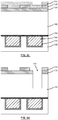
- the figure 1a illustrates the structure of the interconnection lines after etching in a fluorocarbon plasma of the porous material used as dielectric, p-SiOCH, and before filling the trenches 110, as implemented in the conventional so-called "damascene" process for the formation of copper interconnects.
- the etching is done using a hard mask 120, typically made of titanium nitride (TiN), which covers a layer 130 of silicon oxide (SiO 2 ) serving as a stop layer during the mechanical polishing step.
- a hard mask 120 typically made of titanium nitride (TiN)
- SiO 2 silicon oxide
- chemical from the acronym CMP in English for “Chemical Mechanical Polishing”
- CMP chemical Mechanical Polishing
- a layer of porous dielectric material 140 for example of SiOCH
- a layer 150 serving as a stopper layer during plasma etching.
- the global layer 160 symbolizes all the underlying layers of the integrated circuit, in particular those containing active components which are produced during the preliminary stages of the method, those which precede the operations called “BEOL”, acronym for “Back-End Of” Line ”or“ end of line ”stages during which one carries out, at temperatures relatively low, all the levels of interconnections between the active components and where all the dielectric layers are successively etched.
- the figure 1a illustrates a first problem linked to the greater sensitivity of the porous dielectric material 140 during conventional etching in a fluorocarbon plasma. A greater consumption of the porous dielectric material 140 is observed corresponding to an over-etching of this layer 140. Furthermore, it is also possible to encounter problems of moisture absorption which could cause an increase in the dielectric constant of the dielectric material at low permittivity; which goes against the desired goal and also affects the reliability of the device produced.
- the figure 1b illustrates a further problem which relates to the use of a hard metal mask 120.
- the trenches 110 are inevitably exposed to the open air, causing a deposit and formation of residues 170 on the wall of the trenches 110.
- the formation of these residues 170 is all the more important as the trenches 110 are left longer. long in the open.
- the residue formation mechanism 170 is associated with the fluorinated species present on the hard metal mask 120 and on the surfaces of the porous dielectric material 140 with low permittivity, after etching in the fluorocarbon plasma.
- the fluorinated species then react to the humidity of the air producing hydrofluoric acid (HF) which forms metal salts on contact with the hard mask 120.
- HF hydrofluoric acid
- residues 170 affect the quality of the following deposits: that of the barrier layer diffusion of copper, and that of the copper layer which will be used to form all the metallic interconnection lines (the use of copper requires the prior deposition of a layer intended to prevent the diffusion of the latter in the material semiconductor used to make transistors, generally in silicon). These residues 170 can produce unwanted vias between lines (for example, short circuits) and line breaks (for example, open circuits) which very significantly affect the manufacturing efficiency of the devices produced.
- the figure 1c illustrates yet another problem which is linked to humic cleaning based on the use of hydrofluoric acid (HF) and which proves not to be effective enough to remove all the fluorocarbon layer formed when burning.
- fluorine remains on the sides of the trenches 110.
- the fluorine is encapsulated during the deposition of the layer 195 acting as a metal barrier and which must be deposited before the deposition of copper to prevent the latter from migrating. Fluorine tends to diffuse and can lead to degradation of reliability of porous dielectric material 140, eg p-SiOCH.
- Aggressive wet cleaning which would remove the entire fluorine layer, would have the drawback of leading to a loss of definition of the critical dimensions of the devices produced.
- An object of the present invention proposes a method for producing interconnection lines limiting, or even eliminating, at least some of the problems and drawbacks mentioned above, and in particular the problems generated during the step of etching porous dielectric materials at from a plasma based on fluorocarbon compounds.
- the present invention relates to a method according to claim 1.
- the etching step of the method according to the invention makes it possible to form a trench whose sides and the bottom are free of residues.
- limiting residual deposits on the sidewalls improves the conduction quality of the filling material, and therefore promotes the reliability of the interconnection lines.
- the etching is carried out from a plasma comprising at least one hydrocarbon-based gas.
- a plasma comprising at least one hydrocarbon-based gas.
- the gas forming the plasma comprises methane (CH 4 ).
- the protective layer based on hydrocarbon, which develops during the etching, protects the porous dielectric material from any contamination or modification.
- the gas mixture forming the plasma also comprises nitrogen (N 2 ) or oxygen (O 2 ).
- nitrogen makes it possible to etch the porous dielectric material and to control the quantity of carbon deposited on the sidewalls.
- the invention relates to a method of making an electrical interconnection line.
- the method comprises the etching of a pattern forming a trench according to the steps of the invention. It also includes a subsequent step of filling the trench with an electrically conductive material.
- the pattern forms a trench.
- the etching defines a pattern in a layer of porous dielectric material and comprises, prior to the etching, the definition of the pattern in a mask surmounting the layer of porous dielectric material, the etching of the layer of porous dielectric material then being performed through the mask.
- the invention relates to a method for etching at least one pattern in a layer of porous dielectric material.
- the method comprises: defining the pattern in a mask surmounting the layer of porous dielectric material, at least one etching of the layer of porous dielectric material through the mask.
- the etching is carried out in a plasma comprising a gas based on hydrocarbon and nitrogen (N 2 ) or oxygen (O 2 ), so as to form throughout said etching a protective layer, at least on the sides of the layer of porous dielectric material.
- the aim of the invention is to develop a method for producing interconnection lines further comprising a step of chemical etching of a layer of porous dielectric material forming a trench.
- this etching step reduces or even eliminates the damage and / or the formation of residues on the sides of the layer of porous dielectric material.
- the formation of a protective layer on the sides of the layer of porous dielectric material allows the porous dielectric material to retain its electrical properties and in particular low permittivity.
- the limitation of residual deposits and the formation of a protective layer on the sides of the layer of porous dielectric material make it possible to promote conduction of the filling material and thus improve the reliability of the interconnection lines.
- the present invention relates to a method for etching a layer of porous dielectric material.
- the etching is carried out in a plasma so as to grow throughout said etching a protective layer at least on the sides of the layer of porous dielectric material.
- the plasma is formed from a gas formed from a first component and a second component, or from a gas formed from a first component, a second component and a third component.
- the first component is a type C X H Y hydrocarbon, where X is the proportion of carbon in the gas and Y is the proportion of hydrogen (H) in the gas;
- the second component is taken from nitrogen (N 2 ) or dioxygen (O 2 ) or a mixture of nitrogen and dioxygen;
- the third component is taken from argon (Ar) or helium (He).
- the term “on” or “underlying” does not necessarily mean “in contact with”.
- the deposition of a first layer on a second layer does not necessarily mean that the two layers are directly in contact with one another, but it means that the first layer at least partially covers the second layer. by being either directly in contact with it, or by being separated from it by another layer or another element.
- the thicknesses are generally measured in directions perpendicular to the plane of the lower face of the layer to be etched or of a substrate on which the lower layer is placed. Thus the thicknesses are generally taken in a vertical direction in the figures shown. On the other hand, the thickness of a layer covering a side of a pattern is taken in a direction perpendicular to this side.
- the plasma comprises nitrogen (N 2 ).
- the porous dielectric film is etched following nitrogen-based ion bombardment.
- the plasma comprises dioxygen (O 2 ).
- the plasma also comprises argon (Ar) or helium (He).
- the concentration of hydrocarbon forming the plasma is modified.
- the concentration of hydrocarbon forming the plasma is increased to increase the thickness of the protective layer.
- the hydrocarbon-based protective layer formed during the etching electrically insulates the sides of the porous dielectric material.
- the protective layer formed during the etching is kept.
- an additional layer is deposited on the protective layer in order to form interconnections.
- the porous dielectric material is a porous carbon-hydrogen-doped silicon oxide (SiOCH).
- a hard mask is produced surmounting the layer of porous dielectric material, the hard mask having at least one pattern and the etching of the layer of porous dielectric material being performed through the mask hard to transfer the pattern into the porous dielectric material layer.
- the hard mask is made of silicon oxide (SiO 2 ), silicon nitride (SiN) or dense SiOCH.
- the hard mask has a lower face in contact with the layer of porous dielectric material and an upper face opposite the lower face and in which said upper face is in contact with the etching solution during the etching step of the layer of porous dielectric material through the hard mask.
- the thickness of the hard mask is adapted so as not to be entirely consumed during the plasma etching of the layer of porous dielectric material.
- the hard mask is a metal mask.
- a stop layer shaped to stop the etching of the layer of porous dielectric material, and after the step of etching of the layer of porous dielectric material, a step of etching the stopper layer.
- a stopper layer is placed under the layer of porous dielectric material which, when it is subjected to the plasma used to etch the layer of porous dielectric material, has an etching speed lower than the etching speed of the layer of porous dielectric material, and in which the stop layer is etched following the etching of the layer of porous dielectric material using said plasma.
- the pattern is a trench, the method comprising, after the etching of the layer of porous dielectric material, a subsequent step of filling the trench with an electrically conductive material.
- the trench forms an electrical interconnection line.
- the porous dielectric material covers a gate of a transistor and the etching is carried out anisotropically in a main direction parallel to the sides of the gate, so as to remove the layer of porous dielectric material only outside the flanks of the transistor to form spacers for the gate.
- the figure 2 summarizes the steps of etching the porous dielectric material 140 according to the method of the invention and highlights the differences from the standard method.
- the first step is to deposit 210 the various layers of materials including the layer of porous dielectric material 140 in which the interconnection lines are going to be etched.
- the layer 150 serving as an etching stopper layer
- the porous dielectric material layer 140 the oxide layer 130
- the hard metal mask 120 the overall layer 160 or stack of layers symbolizes all of the underlying layers in which the active components, that is to say the transistors, have been made beforehand.
- the next step 220 consists in defining by conventional photolithography, using a photosensitive resin, the patterns of interconnection lines which will have to be etched in the layer of porous dielectric material 140.
- a hard mask is used. metallic 120.
- the patterns are first transferred into the layer 120 generally formed of titanium nitride (TiN).
- TiN titanium nitride
- the patterns defined in the resin layer (not shown) are therefore open in the following step 230 in this layer.
- the use of a hard mask is optional in the context of the present invention.
- the invention differs essentially from the standard method in that the etching of the layer 130 made of SiO 2 , of the layer of porous dielectric material 140 made of porous SiOCH and of the barrier layer 150, which is carried out in step following 250, is done without using fluorinated products.
- the etching of the porous dielectric material layer 140 made of SiOCH in a plasma based on hydrocarbon and nitrogen (N 2 ) and / or oxygen (O 2 ) is carried out. ; said plasma being free of any fluorinated compound.
- the plasma comprises only a hydrocarbon, nitrogen and, optionally but advantageously, argon (Ar) or helium (He).
- the etching operation can be followed by a new wet cleaning step 260 necessary to remove all the impurities present on the surface.
- the figure 3a is a sectional view of a device comprising a first interconnection line at a first level N-1.
- This first interconnection line is preferably formed from a metallic material 180.
- the metallic material is preferably copper.
- the metallization line is protected by an anti-diffusion layer 170.
- This anti-diffusion layer 170 acts as a barrier layer to the diffusion of the metallic material 180 forming the interconnection line.
- This anti-diffusion layer comprises, for example, a bilayer of titanium and titanium nitride, preferably deposited by a vapor deposition technique.
- This first level N-1 is isolated by a barrier layer 150 covered with a new layer of porous dielectric material 140 forming a second level N.
- This barrier layer 150 advantageously plays a protective role preventing contamination of the dielectric material. porous 140 of the second level N by contaminating materials such as copper, which are present in the first level N-1, for example.
- the barrier layer 150 can be formed from materials such as silicon nitride (SiN), nitrided silicon carbide (SiCN), etc.
- a series of steps is required. First of all, an oxide layer 130 is formed on the layer of porous dielectric material 140. Then a layer forming the hard metal mask 120 is produced. In order to form a pattern through, respectively, the hard mask 120, the oxide layer 130 and the porous dielectric material layer 140, a preliminary lithography step is carried out comprising a step of forming a layer 190, preferably resin, on the hard metal mask 120.
- the figure 3b illustrates the step of partial etching of the hard mask 120.
- the titanium nitride (TiN) forming the hard mask 120 is selectively removed by chemical etching based on chlorine (Cl 2 ) in an apparatus dedicated to the etching of the metal in which a chlorinated plasma is formed.
- selective etching of a layer is meant the removal of said layer only at the level of the patterns defined by the previous lithography step, so as to reach a lower layer.
- the figure 3c illustrates a new lithography step consisting in the definition of a pattern defining a trench.
- a layer 192 preferably of resin, is deposited at the end of the step of etching the hard mask 120.
- the pattern is preferably formed at the level of the patterns defined by the previous lithography step.
- the 3d figure illustrates the result of the step of etching the oxide layer 130, preferably silicon dioxide (SiO 2 ), and the porous dielectric material layer 140, so as to form an opening 110 through the layer oxide 130 and the porous dielectric material layer 140.
- oxide layer 130 preferably silicon dioxide (SiO 2 )
- porous dielectric material layer 140 so as to form an opening 110 through the layer oxide 130 and the porous dielectric material layer 140.
- the etching of the oxide layer 130 can be carried out by means of fluorocarbon chemistry. Unlike the conventional process, with the invention, the etching of the porous dielectric material layer 140 made of SiOCH in a plasma based on hydrocarbon and nitrogen (N2) and / or oxygen (O2) is carried out; said plasma being advantageously free of any fluorinated compound.
- the plasma comprises only a hydrocarbon, nitrogen and, optionally but advantageously, argon (Ar) or helium (He).
- it is a physicochemical etching, involving both ion bombardment and a chemical reaction between the ionized gas (plasma) and the surface exposed to ion bombardment.
- the role of nitrogen (N 2 ) is also to etch the porous SiOCH film.
- the hydrocarbon-based gas used during plasma etching, forms a protective envelope at least on the sides of the layer of porous dielectric material 140, leaving a protective layer at least on said sides and the bottom.
- an opening 110 is formed through the oxide layer 130 and the porous dielectric material layer 140.
- the resin layer 192 previously deposited acts as a protective mask for the areas n '. being not intended to be etched, locating the withdrawal of said layers 130, 140 only at the level of the patterns defined by the previous lithography step.
- the removal of the resin layer 192 is, for example, carried out by means of plasma etching using species present in the reactor such as oxygen (O 2 ).
- oxygen (O 2 ) oxygen
- the figure 3e illustrates the result of the step of etching the oxide layer 130 and the layer of porous dielectric material 140.
- the chemistry of the etching of the layer 130 of SiO 2 and of the layer of material porous dielectric 140 can, according to a particular embodiment, also etch the stop layer 150.
- the etching of the oxide layer 130 can be carried out by means of fluorocarbon chemistry.
- the layer of porous dielectric material 140 made of SiOCH is then etched in a plasma based on hydrocarbon and nitrogen (N2) and / or oxygen (O2); said plasma being advantageously free of any fluorinated compound.
- the plasma comprises only a hydrocarbon, nitrogen and, optionally but advantageously, argon (Ar) or helium (He).
- it is a physicochemical etching, involving both ion bombardment and a chemical reaction between the ionized gas (plasma) and the surface exposed to ion bombardment.
- the role of nitrogen (N 2 ) is also to etch the porous SiOCH film.
- the hydrocarbon-based gas used during plasma etching, forms a protective envelope at least on the sides of the layer of porous dielectric material 140, leaving a protective layer 115 at least on said sides and the bottom.
- the hydrocarbon-based protective layer 115 is obtained from a plasma consisting in part of hydrocarbon.
- hydrocarbon is understood to mean organic compounds consisting essentially of carbon and hydrogen.
- the hydrocarbons which can be used in the invention are those of the series of alkanes, alkenes and alkynes. In particular, these hydrocarbons can be saturated or unsaturated.
- hydrocarbons which can be used in the invention mention may be made of acetylene, propadiene, ethylene, butene, propylene, methane, ethane, butane and propane. Preferably, methane is chosen. According to the invention, it is possible to use a hydrocarbon or a mixture of hydrocarbons.
- a protective layer 115 on the sides and the bottom of the trench 112.
- the formation of the protective layer 115 is favored by the fact that the ionic bombardment based on nitrogen on the flanks of the patterns is weak whereas, on the contrary, on the background of the patterns, the bombardment delays the formation of this layer.
- This nitrogen-based ion bombardment is anisotropic, thus making it possible to effectively etch the porous dielectric 140, while maintaining a high aspect ratio.
- the etching chemistry is the same for the layer of porous dielectric material 140 and the barrier layer 150, the layer 150 still acts as a barrier layer. Indeed, the etching speed of the material of the layer 150 is lower than that of the porous dielectric material of the layer 140, in particular due to the porosity of this layer 140.
- the stop layer 150 made, for example, of silicon carbide (SiCH), silicon nitride (SiN) or silicon carbonitride (SiCN).
- the etching of this layer 150 is carried out by means of a traditional fluorocarbon chemistry.
- the etching of the layer 150 is preferably carried out in the same plasma engraver as that of the layer of porous dielectric material.
- the layer of porous dielectric material 140 of p-SiOCH is, in this case, always protected from any contamination by the protective layer 115 which was formed during the previous etching step. It is therefore not altered as in the conventional process.
- the etching of the oxide layer 130, of the porous dielectric material layer 140 and of the stopper layer 150 stops, advantageously on the metallic material 180 forming a metallic line of a first level N-1. Due to the presence of the protective layer 115, the etching takes place without any modification of the layer of porous dielectric material 140.
- a plasma engraver of the ICP or CCP type is preferably used.
- the same equipment is used as for the etching of the oxide layers 130, of porous dielectric material 140 and of stopper 150.
- the ranges of advantageous values of the conditions for carrying out this etching are summarized in the table.
- the porosity of the dielectric material 140 is 25%.
- the etching of the layer of porous dielectric material 140 is based on the fact that the porous SiOCH is etched following the bombardment of the ions generated by the plasma while the protective layer 115, made from hydrocarbon, is spontaneously created on the sides. and the bottom of the trench 112.
- the formation of the protective layer 115 is done with a limited modification of the material constituting the layer of porous dielectric material 140.
- the thickness of the protective layer 115 which is typically included in a range of values going from 1 to 5 nm, and, preferably between 1 and 2 nm, can be adjusted by adjusting the parameters of the plasma during the etching. .
- the important parameters controlling the formation of the passivation layer are: the C X H Y / N 2 ratio, the source power and the bias power which make it possible to control the dissociation rate and the energy of the ions, respectively, in the reactor. CCP or ICP.
- a temperature between 40 ° and 100 ° C is preferred so as to avoid, for excessively low temperatures (typically below 40 ° C), additional deposition of the metal (for example, TiN) contained in the hard mask 120, which can subsequently cause problems of surface roughness as well as stopping the etching.
- the metal for example, TiN
- the etching of the layer of porous dielectric material is carried out using a fluorine-free chemistry such as a gas mixture based on methane (CH 4 ) and nitrogen (N 2 ).
- a fluorine-free chemistry such as a gas mixture based on methane (CH 4 ) and nitrogen (N 2 ).
- the role of nitrogen (N 2 ) is to etch the porous SiOCH film.
- the problem is that if we only use nitrogen (N 2 ), the risk is to modify the flank following ion bombardment. Therefore, the role of methane (CH 4 ) is to protect the side wall (composed of a layer of carbon).
- CH 4 methane the risk is that we will not be able to etch the porous SiOCH film (etch stop) due to the deposit of a too thick carbon layer.
- N 2 also makes it possible to control the deposition of carbon C and by this means to find the compromise between the bottom line of etching by spraying and the lateral protection with a layer of carbon on the sidewall.
- Nitrogen also makes it possible to avoid excessive deposition of polymers.
- the gas ratio between methane and nitrogen must be between 1:20 and 1:10. The risk of using a methane / nitrogen gas mixture ratio greater than 1:10 is to prevent etching of the porous dielectric material 140. The risk of using a methane / nitrogen gas mixture ratio less than 1:20 is modify the porous dielectric material 140.
- oxygen could be suitable as a replacement for nitrogen (N 2 ); this is the case with oxygen (O 2 ), for example.
- oxygen (O 2 ) could cause significant damage to the porous dielectric material layer 140 such as a change in the sidewalls or an increase in the dielectric constant.
- the addition of oxygen must therefore be in a small quantity, in an optimized ratio, in order to limit any deterioration of the porous dielectric material 140.
- the previous etching step is followed by a wet cleaning step.
- this cleaning step does not consume the protective layer 115 formed on the sides of the trench 112 so as to avoid a modification of the layer of porous dielectric material 140.
- the figure 3f illustrates the formation of an anti-diffusion layer 172.
- This anti-diffusion layer 172 is preferably formed from a metallic material.
- this layer 172 comprises a stack of layers or bilayer: a first layer made of a first material such as tantalum and a second layer made of a second material such as tantalum nitride.
- This anti-diffusion layer 172 can be formed by a vapor deposition technique.
- the previous wet cleaning step makes it possible to improve the metallic contact between the metallic anti-diffusion layer 172 of a second level N and the metallic material 180 forming a metallic line of a first level N-1.
- the figure 3g illustrates the step of filling the trenches 112 with a layer 182 of a metallic material.
- the metallic material of the layer 182 is preferably copper. According to a preferred embodiment, an inclination of the sides of the trench 112 promotes, during end-of-line operations, obtaining a satisfactory deposition, on the one hand, of the layer 172 forming a barrier to the diffusion of the material.
- the figure 3h illustrates a final step for the production of interconnection lines comprising a partial removal of the layer 182 in a metallic material.
- this partial removal comprises mechanical-chemical polishing.
- the chemical-mechanical polishing of the layer 182 stops as soon as the porous dielectric material layer 140 is detected.
- no hard metal mask 120 is used; thus steps 230 and 240 of the figure 2 are deleted.
- the layered structure 100 which is deposited in step 210 therefore no longer comprises the layer 120 of titanium nitride (TiN). It is the layer 130, preferably, of silicon oxide which will then serve as a hard mask.
- the conditions for etching the layer of porous dielectric material 140, p-SiOCH are the same as with the hard metal mask 120 and as described in the 3d figures and 3rd .
- the etching differential between the oxide layer 130 and the porous dielectric material layer 140 p-SiOCH being smaller than between the hard metal mask 120, for example of TiN and the porous dielectric material 140, p-SiOCH , it is necessary to provide for a greater consumption of the oxide layer 130 during the etching and to observe a minimum ratio between the thickness of the layer of porous dielectric material 140 to be etched and the thickness of the oxide layer 130.
- the thickness of the oxide layer 130 will be greater than 1/5 of that of the material layer. porous dielectric 140.
- the thickness for each of these layers 130, 140 is measured in a direction perpendicular to the plane in which the layers 130, 140 extend.
- the layer 130, which serves as a hard mask can also be made of carbon (C) or of silicon nitride (SiN).
- the replacement of the traditional etching of the layer of porous dielectric material 140 of p-SiOCH by a non-fluorinated etching advantageously makes it possible not to modify the sides of the trenches 112 of the porous dielectric material 140 during the etching, and not to form residues. fluorides which could possibly make the wet cleaning step after etching unnecessary. In a standard process, these problems lead to a decrease in the reliability of the devices produced.
- the hydrocarbon-based protective layer 115 protects the porous dielectric material 140 throughout the etching.
- this protective layer 115 acts as a diffusion barrier for the precursors.
- an additional layer 172 for example made of metal, is deposited on the protective layer 115 in order to form interconnection lines; the protective layer 115 advantageously remaining in place.
- the variant of the process in which the use of a hard metal mask 120, preferably made of titanium nitride, makes it possible to avoid many associated problems.
Landscapes
- Engineering & Computer Science (AREA)
- Physics & Mathematics (AREA)
- Microelectronics & Electronic Packaging (AREA)
- General Physics & Mathematics (AREA)
- Manufacturing & Machinery (AREA)
- Computer Hardware Design (AREA)
- Condensed Matter Physics & Semiconductors (AREA)
- Power Engineering (AREA)
- Chemical & Material Sciences (AREA)
- Inorganic Chemistry (AREA)
- Chemical Kinetics & Catalysis (AREA)
- General Chemical & Material Sciences (AREA)
- Plasma & Fusion (AREA)
- Internal Circuitry In Semiconductor Integrated Circuit Devices (AREA)
Description
La présente invention est relative à l'utilisation de matériaux diélectriques poreux à faible permittivité pour la réalisation de lignes d'interconnexion électriques pour des dispositifs microélectroniques et notamment dans les circuits intégrés. Elle concerne, plus particulièrement, un procédé de gravure amélioré de tels matériaux.The present invention relates to the use of porous dielectric materials with low permittivity for the production of electrical interconnection lines for microelectronic devices and in particular in integrated circuits. It relates more particularly to an improved etching process for such materials.
Afin de répondre aux exigences de taille des dispositifs et de temps de commutation en microélectronique, le procédé de réalisation de lignes d'interconnexion, lesquelles lignes nécessitant une isolation par un matériau diélectrique poreux, a dû être adapté. En outre, la réalisation de tranchées étroites dans le matériau diélectrique poreux, SiOCH par exemple, nécessite de revoir les différents procédés par plasma (gravure, traitements post-gravure) et les schémas d'intégration, puisque ce matériau est connu pour être facilement dégradé lorsqu'il est exposé à un plasma à base de fluor, notamment. Les études faites pour évaluer l'efficacité de différents plasmas en fonction des matériaux exposés aux plasmas permettent de caractériser et d'optimiser les procédés de transfert de motifs d'un masque métallique ou organique dans un SiOCH poreux ou hybride (rendu poreux en fin d'intégration). Un problème majeur est la modification des matériaux diélectriques poreux et hybrides lors de plasma « post-gravure ». Avec un plasma fluorocarboné, le matériau hybride présente des mécanismes de gravure similaires à ceux d'un SiOCH dense. Le matériau de type nitrure de titane (TiN) et le matériau organique ont des mécanismes de gravure différents de ceux des diélectriques, ce qui assure une bonne sélectivité. Le procédé de gravure optimisé pour le masque organique permet la gravure de tranchées très étroites avec un profil quasiment vertical.In order to meet the requirements of the size of the devices and of the switching time in microelectronics, the method of producing interconnection lines, which lines requiring insulation by a porous dielectric material, had to be adapted. In addition, the realization of narrow trenches in the porous dielectric material, SiOCH for example, requires reviewing the different plasma processes (etching, post-etching treatments) and the integration schemes, since this material is known to be easily degraded. when exposed to a fluorine-based plasma, in particular. The studies carried out to evaluate the efficiency of different plasmas according to the materials exposed to the plasmas make it possible to characterize and optimize the pattern transfer processes of a metallic or organic mask in a porous or hybrid SiOCH (made porous at the end of 'integration). A major problem is the modification of porous and hybrid dielectric materials during “post-etching” plasma. With fluorocarbon plasma, the hybrid material exhibits etching mechanisms similar to those of dense SiOCH. The titanium nitride (TiN) type material and the organic material have different etching mechanisms from those of dielectrics, which ensures good selectivity. The etching process optimized for the organic mask allows the etching of very narrow trenches with an almost vertical profile.
Lors du procédé de réalisation de lignes d'interconnexion, une des étapes critiques demeure la gravure de la couche de matériau diélectrique poreux. Le principal inconvénient d'une gravure plasma à base de fluor dans un dispositif comprenant un masque dur métallique et une couche de matériau diélectrique poreux est la génération de résidus provenant de l'interaction entre des espèces chimiques présentes dans le plasma et sur le masque métallique ; lesdits résidus se déposant sur les couches et provoquant par la suite des défaillances des dispositifs réalisés. Ce phénomène de formation de résidus lors d'une gravure plasma à base de fluor et de carbone est notamment décrit dans la publication en anglais :
Dans le document de
Dans le document
D'autres inconvénients de la gravure plasma à base de fluor sont évoqués ci-après et illustrés dans les
La
La gravure se fait en utilisant un masque dur 120, typiquement fait de nitrure de titane (TiN), qui recouvre une couche 130 d'oxyde de silicium (SiO2) servant de couche d'arrêt lors de l'étape de polissage mécano-chimique (de l'acronyme CMP en anglais pour « Chemical Mechanical Polishing ») en vue de la réalisation ultérieure de lignes d'interconnexion à base de cuivre par exemple avec le procédé « damascène ». Préalablement au dépôt de la couche 130 d'oxyde de silicium, est formée une couche de matériau diélectrique poreux 140, par exemple de SiOCH. Sous la couche de matériau diélectrique poreux 140 se trouve une couche 150 servant de couche d'arrêt lors de la gravure plasma. La couche globale 160 symbolise toutes les couches sous-jacentes du circuit intégré, notamment celles contenant des composants actifs qui sont réalisés lors des étapes préliminaires du procédé, celles qui précèdent les opérations dites « BEOL » acronyme de l'anglais « Back-End Of Line » ou étapes de « fin de ligne » au cours desquelles on réalise, à des températures relativement faibles, tous les niveaux d'interconnexions entre les composants actifs et où l'on va graver successivement toutes les couches diélectriques.The etching is done using a
La
La
La
Par conséquent, l'introduction de matériaux diélectriques poreux à faible permittivité nécessaire pour réduire la constante de temps des interconnexions entre composants actifs d'un circuit intégré, et notamment la gravure de ces matériaux diélectriques poreux dans un plasma fluorocarboné, posent de nombreux problèmes.Consequently, the introduction of porous dielectric materials with low permittivity necessary to reduce the time constant of the interconnections between active components of an integrated circuit, and in particular the etching of these porous dielectric materials in a fluorocarbon plasma, pose numerous problems.
Un objet de la présente invention propose un procédé de réalisation de lignes d'interconnexion limitant, voire supprimant, au moins certains des problèmes et inconvénients mentionnés ci-dessus, et notamment les problèmes générés lors de l'étape de gravure de matériaux diélectriques poreux à partir d'un plasma à base de composés fluorocarbonés.An object of the present invention proposes a method for producing interconnection lines limiting, or even eliminating, at least some of the problems and drawbacks mentioned above, and in particular the problems generated during the step of etching porous dielectric materials at from a plasma based on fluorocarbon compounds.
La présente invention concerne un procédé selon la revendication 1.The present invention relates to a method according to claim 1.
De manière particulièrement avantageuse, l'étape de gravure du procédé selon l'invention permet de former une tranchée dont les flancs et le fond sont dépourvus de résidus. Ainsi, lors de l'étape de remplissage des tranchées, la limitation de dépôts résiduels sur les flancs améliore la qualité de conduction du matériau de remplissage, et de ce fait, favorise la fiabilité des lignes d'interconnexion.In a particularly advantageous manner, the etching step of the method according to the invention makes it possible to form a trench whose sides and the bottom are free of residues. Thus, during the step of filling the trenches, limiting residual deposits on the sidewalls improves the conduction quality of the filling material, and therefore promotes the reliability of the interconnection lines.
La gravure est réalisée à partir d'un plasma comprenant au moins un gaz à base d'hydrocarbure. Avantageusement, tous les composées de type CXHY, où X est la proportion de carbone et Y la proportion d'hydrogène, sont susceptibles de convenir. A titre préféré, le gaz formant le plasma comprend du méthane (CH4).The etching is carried out from a plasma comprising at least one hydrocarbon-based gas. Advantageously, all compounds of type C X H Y , where X is the proportion of carbon and Y the proportion of hydrogen, are likely to be suitable. Preferably, the gas forming the plasma comprises methane (CH 4 ).
De manière particulièrement avantageuse, la couche de protection, à base d'hydrocarbure, qui se développe pendant la gravure, protège le matériau diélectrique poreux de toute contamination ou modification.In a particularly advantageous manner, the protective layer, based on hydrocarbon, which develops during the etching, protects the porous dielectric material from any contamination or modification.
Le mélange de gaz formant le plasma comprend également de l'azote (N2) ou de l'oxygène (O2). En outre, l'azote permet de graver le matériau diélectrique poreux et de contrôler la quantité de carbone déposé sur les flancs.The gas mixture forming the plasma also comprises nitrogen (N 2 ) or oxygen (O 2 ). In addition, nitrogen makes it possible to etch the porous dielectric material and to control the quantity of carbon deposited on the sidewalls.
L'invention porte sur un procédé de réalisation d'une ligne d'interconnexion électrique. Le procédé comprend la gravure d'un motif formant une tranchée selon les étapes de l'invention. Il comprend également une étape ultérieure de remplissage de la tranchée par un matériau électriquement conducteur.The invention relates to a method of making an electrical interconnection line. The method comprises the etching of a pattern forming a trench according to the steps of the invention. It also includes a subsequent step of filling the trench with an electrically conductive material.
Le motif forme une tranchée.The pattern forms a trench.
Selon une option, la gravure définit un motif dans une couche de matériau diélectrique poreux et comprend, préalablement à la gravure, la définition du motif dans un masque surmontant la couche de matériau diélectrique poreux, la gravure de la couche de matériau diélectrique poreux étant ensuite effectuée à travers le masque.According to one option, the etching defines a pattern in a layer of porous dielectric material and comprises, prior to the etching, the definition of the pattern in a mask surmounting the layer of porous dielectric material, the etching of the layer of porous dielectric material then being performed through the mask.
Selon un autre mode de réalisation, l'invention porte sur un procédé de gravure d'au moins un motif dans une couche de matériau diélectrique poreux. Le procédé comprend : la définition du motif dans un masque surmontant la couche de matériau diélectrique poreux, au moins une gravure de la couche de matériau diélectrique poreux à travers le masque. La gravure est réaliseé dans un plasma comprenant un gaz à base d'hydrocarbure et d'azote (N2) ou d'oxygène (O2), de manière à former tout au long de ladite gravure une couche de protection, au moins sur les flancs de la couche de matériau diélectrique poreux.According to another embodiment, the invention relates to a method for etching at least one pattern in a layer of porous dielectric material. The method comprises: defining the pattern in a mask surmounting the layer of porous dielectric material, at least one etching of the layer of porous dielectric material through the mask. The etching is carried out in a plasma comprising a gas based on hydrocarbon and nitrogen (N 2 ) or oxygen (O 2 ), so as to form throughout said etching a protective layer, at least on the sides of the layer of porous dielectric material.
Le but de l'invention est de développer un procédé de réalisation de lignes d'interconnexion comprenant en outre une étape de gravure chimique d'une couche de matériau diélectrique poreux formant une tranchée. Avantageusement, cette étape de gravure réduit voire supprime les dommages et/ou la formation de résidus sur les flancs de la couche de matériau diélectrique poreux.The aim of the invention is to develop a method for producing interconnection lines further comprising a step of chemical etching of a layer of porous dielectric material forming a trench. Advantageously, this etching step reduces or even eliminates the damage and / or the formation of residues on the sides of the layer of porous dielectric material.
Avantageusement, la formation d'une couche de protection sur les flancs de la couche de matériau diélectrique poreux permet, au matériau diélectrique poreux, de conserver ses propriétés électriques et notamment une faible permittivité. De manière particulièrement avantageuse, la limitation de dépôts résiduels et la formation d'une couche de protection sur les flancs de la couche de matériau diélectrique poreux permettent de favoriser la conduction du matériau de remplissage et ainsi améliorent la fiabilité des lignes d'interconnexion.Advantageously, the formation of a protective layer on the sides of the layer of porous dielectric material allows the porous dielectric material to retain its electrical properties and in particular low permittivity. In a particularly advantageous manner, the limitation of residual deposits and the formation of a protective layer on the sides of the layer of porous dielectric material make it possible to promote conduction of the filling material and thus improve the reliability of the interconnection lines.
Selon un autre mode de réalisation, la présente invention concerne un procédé de gravure d'une couche de matériau diélectrique poreux. La gravure est réalisée dans un plasma de manière à faire croître tout au long de ladite gravure une couche de protection au moins sur des flancs de la couche de matériau diélectrique poreux. Le plasma est formé à partir d'un gaz formé d'un premier composant et d'un deuxième composant, ou d'un gaz formé d'un premier composant, d'un deuxième composant et d'un troisième composant. Le premier composant est un hydrocarbure de type CXHY, où X est la proportion de carbone dans le gaz et Y la proportion d'hydrogène (H) dans le gaz ; le deuxième composant est pris parmi l'azote (N2) ou le dioxygène (O2) ou un mélange d'azote et de dioxygène ; le troisième composant est pris parmi l'argon (Ar) ou l'hélium (He).According to another embodiment, the present invention relates to a method for etching a layer of porous dielectric material. The etching is carried out in a plasma so as to grow throughout said etching a protective layer at least on the sides of the layer of porous dielectric material. The plasma is formed from a gas formed from a first component and a second component, or from a gas formed from a first component, a second component and a third component. The first component is a type C X H Y hydrocarbon, where X is the proportion of carbon in the gas and Y is the proportion of hydrogen (H) in the gas; the second component is taken from nitrogen (N 2 ) or dioxygen (O 2 ) or a mixture of nitrogen and dioxygen; the third component is taken from argon (Ar) or helium (He).
Les buts, objets, ainsi que les caractéristiques et avantages de l'invention ressortiront mieux de la description détaillée d'un mode de réalisation de cette dernière qui est illustré par les dessins d'accompagnement suivants dans lesquels :
- Les
FIGURES 1a à 1c illustrent les différents problèmes générés par la gravure du matériau diélectrique poreux, par exemple le p-SIOCH, à partir d'un plasma fluorocarboné. - La
FIGURE 2 résume les étapes principales du procédé de l'invention et les différences d'avec le procédé standard de gravure du matériau diélectrique poreux, pour y former des tranchées. - Les
FIGURES 3a à 3h illustrent les différentes étapes du procédé de l'invention en vue de la réalisation de lignes d'interconnexion.
- The
FIGURES 1a to 1c illustrate the various problems generated by the etching of the porous dielectric material, for example p-SIOCH, from a fluorocarbon plasma. - The
FIGURE 2 summarizes the main steps of the process of the invention and the differences with the standard process for etching the porous dielectric material, to form trenches therein. - The
FIGURES 3a to 3h illustrate the different steps of the method of the invention with a view to producing interconnection lines.
Les dessins sont donnés à titre d'exemples et ne sont pas limitatifs de l'invention. Ils constituent des représentations schématiques de principe destinées à faciliter la compréhension de l'invention et ne sont pas nécessairement à l'échelle des applications pratiques. En particulier, les épaisseurs relatives des différentes couches et films ne sont pas représentatives de la réalité.The drawings are given by way of example and do not limit the invention. They constitute schematic representations of principle intended to facilitate understanding of the invention and are not necessarily on the scale of practical applications. In particular, the relative thicknesses of the various layers and films are not representative of reality.
Il est précisé que dans le cadre de la présente invention, le terme « sur » ou « sous-jacent » ne signifient pas obligatoirement « au contact de ». Ainsi, par exemple, le dépôt d'une première couche sur une deuxième couche , ne signifie pas obligatoirement que les deux couches sont directement au contact l'une de l'autre mais cela signifie que la première couche recouvre au moins partiellement la deuxième couche en étant soit directement à son contact, soit en étant séparée d'elle par une autre couche ou un autre élément.It is specified that in the context of the present invention, the term “on” or “underlying” does not necessarily mean “in contact with”. Thus, for example, the deposition of a first layer on a second layer does not necessarily mean that the two layers are directly in contact with one another, but it means that the first layer at least partially covers the second layer. by being either directly in contact with it, or by being separated from it by another layer or another element.
Dans la description qui suit, les épaisseurs sont généralement mesurées selon des directions perpendiculaires au plan de la face inférieure de la couche à graver ou d'un substrat sur lequel la couche inférieure est disposée. Ainsi les épaisseurs sont généralement prises selon une direction verticale sur les figures représentées. En revanche, l'épaisseur d'une couche recouvrant un flanc d'un motif est prise selon une direction perpendiculaire à ce flanc.In the following description, the thicknesses are generally measured in directions perpendicular to the plane of the lower face of the layer to be etched or of a substrate on which the lower layer is placed. Thus the thicknesses are generally taken in a vertical direction in the figures shown. On the other hand, the thickness of a layer covering a side of a pattern is taken in a direction perpendicular to this side.
Avant d'entamer une revue détaillée de modes de réalisation de l'invention, sont énoncées ci-après des caractéristiques optionnelles qui peuvent éventuellement être en association ou alternativement :
- Selon un mode de réalisation particulièrement avantageux, le ratio de gaz entre le premier composant et le deuxième composant est compris entre 5% et 20%
- Selon un mode de réalisation particulièrement avantageux, le ratio de gaz entre le premier composant et le deuxième composant est supérieur à 1:20 et inférieur à 1:10. Le risque d'utiliser un ratio de mélange gazeux, par exemple de méthane/azote, supérieur à 1:10 est d'empêcher la gravure du matériau diélectrique poreux. Le risque d'utiliser un ratio de mélange gazeux, par exemple de méthane/azote, inférieur à 1:20 est de modifier le matériau diélectrique poreux. Typiquement le ratio est un rapport du débit du premier composant sur le début du deuxième composant. Ces débits peuvent s'exprimer en sscm acronyme de l'anglais standard cubic centimeters per minute signifiant centimètres cubiques standard par minute.
- According to a particularly advantageous embodiment, the gas ratio between the first component and the second component is between 5% and 20%
- According to a particularly advantageous embodiment, the gas ratio between the first component and the second component is greater than 1:20 and less than 1:10. The risk of using a gas mixture ratio, for example methane / nitrogen, greater than 1:10 is to prevent etching of the porous dielectric material. The risk of using a gas mixture ratio, for example methane / nitrogen, of less than 1:20 is to modify the porous dielectric material. Typically the ratio is a ratio of the flow rate of the first component to the start of the second component. These flow rates can be expressed in sscm acronym for standard English cubic centimeters per minute meaning standard cubic centimeters per minute.
Avantageusement, le plasma comprend de l'azote (N2). Le film diélectrique poreux est gravé suite au bombardement ionique à base d'azote.Advantageously, the plasma comprises nitrogen (N 2 ). The porous dielectric film is etched following nitrogen-based ion bombardment.
Selon un mode de réalisation, le plasma comprend du dioxygène (O2).According to one embodiment, the plasma comprises dioxygen (O 2 ).
Avantageusement, le plasma comprend également de l'argon (Ar) ou de l'hélium (He).Advantageously, the plasma also comprises argon (Ar) or helium (He).
De préférence, pour ajuster l'épaisseur de la couche de protection, on modifie la concentration en hydrocarbure formant le plasma. Typiquement, on augmente la concentration en hydrocarbure formant le plasma pour augmenter l'épaisseur de la couche de protection. Il convient cependant de ne pas avoir une concentration trop élevée pour ne pas empêcher la gravure.Preferably, to adjust the thickness of the protective layer, the concentration of hydrocarbon forming the plasma is modified. Typically, the concentration of hydrocarbon forming the plasma is increased to increase the thickness of the protective layer. However, it is advisable not to have too high a concentration so as not to prevent etching.
De manière particulièrement avantageuse, la couche de protection à base d'hydrocarbure formée lors de la gravure isole électriquement les flancs du matériau diélectrique poreux.In a particularly advantageous manner, the hydrocarbon-based protective layer formed during the etching electrically insulates the sides of the porous dielectric material.
Avantageusement, on conserve la couche de protection formée lors de la gravure. Selon un mode de réalisation, on dépose une couche additionnelle sur la couche de protection afin de former des interconnexions.Advantageously, the protective layer formed during the etching is kept. According to one embodiment, an additional layer is deposited on the protective layer in order to form interconnections.
Le matériau diélectrique poreux est un oxyde de silicium dopé au carbone et à l'hydrogène (SiOCH) poreux.The porous dielectric material is a porous carbon-hydrogen-doped silicon oxide (SiOCH).
Avantageusement, avant la gravure de la couche de matériau diélectrique poreux, on réalise un masque dur surmontant la couche de matériau diélectrique poreux, le masque dur présentant au moins un motif et la gravure de la couche de matériau diélectrique poreux étant effectuée à travers le masque dur pour transférer le motif dans la couche de matériau diélectrique poreux.Advantageously, before the etching of the layer of porous dielectric material, a hard mask is produced surmounting the layer of porous dielectric material, the hard mask having at least one pattern and the etching of the layer of porous dielectric material being performed through the mask hard to transfer the pattern into the porous dielectric material layer.
De préférence, le masque dur est fait d'oxyde de silicium (SiO2), de nitrure de silicium (SiN) ou de SiOCH dense.Preferably, the hard mask is made of silicon oxide (SiO 2 ), silicon nitride (SiN) or dense SiOCH.
Avantageusement, le masque dur présente une face inférieure au contact de la couche de matériau diélectrique poreux et une face supérieure opposée à la face inférieure et dans lequel ladite face supérieure est au contact de la solution de gravure lors de l'étape de gravure de la couche de matériau diélectrique poreux à travers le masque dur.Advantageously, the hard mask has a lower face in contact with the layer of porous dielectric material and an upper face opposite the lower face and in which said upper face is in contact with the etching solution during the etching step of the layer of porous dielectric material through the hard mask.
Avantageusement, l'épaisseur du masque dur est adaptée pour ne pas être entièrement consommé pendant la gravure plasma de la couche de matériau diélectrique poreux.Advantageously, the thickness of the hard mask is adapted so as not to be entirely consumed during the plasma etching of the layer of porous dielectric material.
Préférentiellement, le masque dur est un masque métallique.Preferably, the hard mask is a metal mask.
Avantageusement, préalablement à la définition du motif dans le masque dur, on dispose, sous la couche de matériau diélectrique poreux, une couche d'arrêt conformée pour stopper la gravure de la couche de matériau diélectrique poreux, et on effectue après l'étape de gravure de la couche de matériau diélectrique poreux, une étape de gravure de la couche d'arrêt.Advantageously, prior to the definition of the pattern in the hard mask, there is placed, under the layer of porous dielectric material, a stop layer shaped to stop the etching of the layer of porous dielectric material, and after the step of etching of the layer of porous dielectric material, a step of etching the stopper layer.
Selon un mode de réalisation, préalablement à la définition du motif du masque dur, on dispose sous la couche de matériau diélectrique poreux une couche d'arrêt qui, lorsqu'elle est soumise au plasma utilisé pour graver la couche de matériau diélectrique poreux, présente une vitesse de gravure inférieure à la vitesse de gravure de la couche de matériau diélectrique poreux, et dans lequel on grave la couche d'arrêt à la suite de la gravure de la couche de matériau diélectrique poreux en utilisant ledit plasma.According to one embodiment, prior to the definition of the pattern of the hard mask, a stopper layer is placed under the layer of porous dielectric material which, when it is subjected to the plasma used to etch the layer of porous dielectric material, has an etching speed lower than the etching speed of the layer of porous dielectric material, and in which the stop layer is etched following the etching of the layer of porous dielectric material using said plasma.
Avantageusement, le motif est une tranchée, le procédé comprenant, après la gravure de la couche de matériau diélectrique poreux, une étape ultérieure de remplissage de la tranchée par un matériau électriquement conducteur.Advantageously, the pattern is a trench, the method comprising, after the etching of the layer of porous dielectric material, a subsequent step of filling the trench with an electrically conductive material.
De préférence, la tranchée forme une ligne d'interconnexion électrique.Preferably, the trench forms an electrical interconnection line.
Avantageusement, avant l'étape de gravure, le matériau diélectrique poreux recouvre une grille d'un transistor et la gravure est effectuée de manière anisotrope selon une direction principale parallèle à des flancs de la grille, de sorte à retirer la couche de matériau diélectrique poreux uniquement en dehors des flancs du transistor pour former des espaceurs pour la grille.Advantageously, before the etching step, the porous dielectric material covers a gate of a transistor and the etching is carried out anisotropically in a main direction parallel to the sides of the gate, so as to remove the layer of porous dielectric material only outside the flanks of the transistor to form spacers for the gate.
La
On procède tout d'abord au dépôt 210 des différentes couches de matériaux incluant la couche de matériau diélectrique poreux 140 dans laquelle on va graver les lignes d'interconnexion. On retrouve les différentes couches déjà décrites qui sont, dans l'ordre où elles sont déposées: la couche 150 servant de couche d'arrêt à la gravure, la couche de matériau diélectrique poreux 140, la couche d'oxyde 130, le masque dur 120 métallique. Dans cette structure stratifiée 100, la couche globale 160 ou empilement de couches symbolise l'ensemble des couches sous-jacentes dans lesquelles ont été préalablement réalisés les composants actifs c'est-à-dire les transistors.The first step is to deposit 210 the various layers of materials including the layer of porous
De manière avantageuse mais non limitative, les épaisseurs et matériaux des couches ci-dessus sont :
- Le masque dur 120 métallique est préférentiellement formé à base de nitrure de silicium (TiN), dans une gamme d'épaisseur comprise entre 5 et 100 nanomètres (nm) et, de préférence, entre 10 et 50 nm. Dans le cadre de la présente invention, le masque dur 120 métallique peut également être réalisé en nitrure de tantale (TaN) ou en nitrure de bore (BN).
- La couche 130 d'oxyde est, de préférence, à base d'oxyde de silicium (SiO2), dans une gamme d'épaisseur allant de 10 à 50 nm. Elle sert de couche d'arrêt pour l'étape de polissage mécano-chimique (CMP) qui est effectuée lors de la formation des interconnexions avec le procédé « damascène ».
- La couche de matériau diélectrique poreux 140 est formée à base de SiOCH poreux. Son épaisseur est comprise entre 50 et 120 nm. Cette couche peut être déposée par centrifugation, opération qui est généralement qualifiée du terme anglais de « spin coating », c'est-à-dire d'un dépôt par étalement à l'aide d'une « tournette ». Le dépôt de SiOCH se fait sous forme liquide sur la tranche en rotation et dans sa forme poreuse finale. On peut aussi procéder par voie sèche à un « dépôt chimique en phase vapeur assisté par plasma » ou « PECVD » acronyme en l'anglais de « plasma-enhanced chemical vapor déposition ». Le dépôt se fait alors en deux étapes à partir de deux gaz précurseurs : l'un pour générer la matrice dense de matériau diélectrique poreux SiOCH, l'autre pour former la structure porogène dans laquelle on peut faire varier la proportion volumique de pores. Dans les deux cas, la porosité du matériau diélectrique 140 est, de préférence, comprise entre 10% et 50% de sorte à assurer une bonne efficacité de la gravure. La chimie de la gravure de l'invention n'est pas limitée au matériau diélectrique poreux
SiOCH. Elle peut également se pratiquer avec d'autres matériaux tels que l'oxyde de silicium (SiO2) et le nitrure de silicium (SiN). - La couche 150 d'arrêt de gravure est typiquement d'une épaisseur allant de 10 à 20 nm. Elle peut être constituée des matériaux suivants utilisés de façon standard pour les opérations de fin de ligne de fabrication (BEOL) : carbure de silicium (SiCH), nitrure de silicium (SiN) ou carbonitrure de silicium (SiCN). La couche 150 d'arrêt joue avantageusement un rôle de protection empêchant la contamination du matériau diélectrique poreux 140 par des matériaux contaminants tels que le cuivre, qui sont présents dans les niveaux inférieurs, c'est-à-dire dans les couches sous-jacentes de la couche globale 160.
- The hard
metallic mask 120 is preferably formed based on silicon nitride (TiN), in a thickness range of between 5 and 100 nanometers (nm) and, preferably, between 10 and 50 nm. In the context of the present invention, thehard metal mask 120 can also be made of tantalum nitride (TaN) or of boron nitride (BN). - The
oxide layer 130 is preferably based on silicon oxide (SiO 2 ), in a thickness range going from 10 to 50 nm. It serves as a barrier layer for the chemical-mechanical polishing (CMP) step which is carried out during the formation of the interconnections with the "damascene" process. - The porous
dielectric material layer 140 is formed based on porous SiOCH. Its thickness is between 50 and 120 nm. This layer can be deposited by centrifugation, an operation which is generally referred to by the English term as “spin coating”, that is to say a deposit by spreading using a “spinner”. The SiOCH is deposited in liquid form on the rotating wafer and in its final porous form. A “plasma-assisted chemical vapor deposition” or “PECVD” acronym for “plasma-enhanced chemical vapor deposition” can also be carried out by the dry route. The deposition is then carried out in two stages from two precursor gases: one to generate the dense matrix of porous dielectric material SiOCH, the other to form the pore-forming structure in which the volume proportion of pores can be varied. In both cases, the porosity of thedielectric material 140 is preferably between 10% and 50% so as to ensure good efficiency of the etching. The chemistry of the etching of the invention is not limited to the porous dielectric material
SiOCH. It can also be practiced with other materials such as silicon oxide (SiO 2 ) and silicon nitride (SiN). - The
etch stop layer 150 is typically of a thickness ranging from 10 to 20 nm. It can be made of the following materials used as standard for end of production line operations (BEOL): silicon carbide (SiCH), silicon nitride (SiN) or silicon carbonitride (SiCN). Thebarrier layer 150 advantageously plays a protective role preventing contamination of the porousdielectric material 140 by contaminating materials such as copper, which are present in the lower levels, that is to say in the underlying layers. of theglobal layer 160.
L'étape suivante 220 consiste à définir par photolithographie classique, en utilisant une résine photosensible, les motifs de lignes d'interconnexion qui vont devoir être gravés dans la couche de matériau diélectrique poreux 140. Pour ce faire, on a recours à un masque dur métallique 120. Les motifs sont d'abord transférés dans la couche 120 généralement formée de nitrure de titane (TiN). Les motifs définis dans la couche de résine (non représentée) sont donc ouverts à l'étape suivante 230 dans cette couche. L'utilisation d'un masque dur est optionnelle dans le cadre de la présente invention. Ces étapes sont suivies d'une étape de nettoyage par voie humide 240.The
L'invention diffère essentiellement du procédé standard en ce que la gravure de la couche 130 faite de SiO2, de la couche de matériau diélectrique poreux 140 faite de SiOCH poreux et de la couche 150 d'arrêt, qui est réalisée à l'étape suivante 250, se fait sans mettre en œuvre de produits fluorés.The invention differs essentially from the standard method in that the etching of the
Comme cela sera expliqué par la suite, on réalise la gravure de la couche de matériau diélectrique poreux 140 poreux faite de SiOCH dans un plasma à base d'hydrocarbure et d'azote (N2) et/ou d'oxygène (O2) ; ledit plasma étant exempt de tout composé fluoré. De préférence, et dans l'exemple ci-dessous, le plasma comprend uniquement un hydrocarbure, de l'azote et, de manière optionnelle mais avantageuse, de l'argon (Ar) ou de l'hélium (He).As will be explained later, the etching of the porous
Dans les deux cas, l'opération de gravure peut être suivie d'une nouvelle étape de nettoyage par voie humide 260 nécessaire pour retirer toutes les impuretés présentes en surface.In both cases, the etching operation can be followed by a new
Les
La
Afin de réaliser une deuxième ligne d'interconnexion au deuxième niveau N, à partir de la couche de matériau diélectrique poreux 140, une série d'étapes est requise. On forme tout d'abord une couche d'oxyde 130 sur la couche de matériau diélectrique poreux 140. Ensuite une couche formant le masque dur 120 métallique est réalisée. Afin de former un motif au travers, respectivement, du masque dur 120, de la couche d'oxyde 130 et de la couche de matériau diélectrique poreux 140, on réalise une étape préliminaire de lithographie comprenant une étape de formation d'une couche 190, de préférence de résine, sur le masque dur 120 métallique.In order to produce a second interconnection line at the second level N, from the layer of porous
La
La
La
La gravure de la couche d'oxyde 130 peut être réalisée au moyen d'une chimie fluoro-carbonée. Contrairement au procédé conventionnel, avec l'invention, on réalise la gravure de la couche de matériau diélectrique poreux 140 faite de SiOCH dans un plasma à base d'hydrocarbure et d'azote (N2) et/ou d'oxygène (O2) ; ledit plasma étant avantageusement exempt de tout composé fluoré. De préférence, et dans l'exemple ci-dessous, le plasma comprend uniquement un hydrocarbure, de l'azote et, de manière optionnelle mais avantageuse, de l'argon (Ar) ou de l'hélium (He).The etching of the
Avantageusement, il s'agit d'une gravure physico-chimique, mettant en jeu à la fois un bombardement ionique et une réaction chimique entre le gaz ionisé (plasma) et la surface exposée au bombardement ionique. Le rôle de l'azote (N2) est en outre de graver le film de SiOCH poreux.Advantageously, it is a physicochemical etching, involving both ion bombardment and a chemical reaction between the ionized gas (plasma) and the surface exposed to ion bombardment. The role of nitrogen (N 2 ) is also to etch the porous SiOCH film.
Le gaz à base d'hydrocarbure, utilisé lors de la gravure plasma, forme une enveloppe protectrice au moins sur les flancs de la couche de matériau diélectrique poreux 140, laissant une couche de protection au moins sur lesdits flancs et le fond.The hydrocarbon-based gas, used during plasma etching, forms a protective envelope at least on the sides of the layer of porous
A l'issue de cette gravure, une ouverture 110 est formée au travers de la couche d'oxyde 130 et de la couche de matériau diélectrique poreux 140. La couche de résine 192 préalablement déposée fait office de masque de protection pour les zones n'étant pas destinées à être gravées, localisant le retrait desdites couches 130, 140 uniquement au niveau des motifs définis par la précédente étape de lithographie. Il s'ensuit une étape de retrait de la couche de résine 192. Le retrait de la couche de résine 192 est, par exemple, réalisé à l'aide d'une gravure plasma au moyen d'espèces présentes dans le réacteur comme l'oxygène (O2). Lors du retrait de la couche de résine 192, la couche de protection formée au moins sur les flancs et le fond de l'ouverture 110 est retirée.At the end of this etching, an
La
Comme précédemment, la gravure de la couche d'oxyde 130 peut être réalisée au moyen d'une chimie fluoro-carbonée. On réalise ensuite la gravure de la couche de matériau diélectrique poreux 140 faite de SiOCH, dans un plasma à base d'hydrocarbure et d'azote (N2) et/ou d'oxygène (O2) ; ledit plasma étant avantageusement exempt de tout composé fluoré. De préférence, et dans l'exemple ci-dessous, le plasma comprend uniquement un hydrocarbure, de l'azote et, de manière optionnelle mais avantageuse, de l'argon (Ar) ou de l'hélium (He).As previously, the etching of the
Avantageusement, il s'agit d'une gravure physico-chimique, mettant en jeu à la fois un bombardement ionique et une réaction chimique entre le gaz ionisé (plasma) et la surface exposée au bombardement ionique. Le rôle de l'azote (N2) est en outre de graver le film de SiOCH poreux.Advantageously, it is a physicochemical etching, involving both ion bombardment and a chemical reaction between the ionized gas (plasma) and the surface exposed to ion bombardment. The role of nitrogen (N 2 ) is also to etch the porous SiOCH film.
Le gaz à base d'hydrocarbure, utilisé lors de la gravure plasma, forme une enveloppe protectrice au moins sur les flancs de la couche de matériau diélectrique poreux 140, laissant une couche de protection 115 au moins sur lesdits flancs et le fond.The hydrocarbon-based gas, used during plasma etching, forms a protective envelope at least on the sides of the layer of porous
La couche de protection 115 à base d'hydrocarbure est obtenue à partir d'un plasma constitué en partie d'hydrocarbure. Par hydrocarbure, on entend les composés organiques constitués essentiellement de carbone et d'hydrogène. Les hydrocarbures utilisables dans l'invention sont ceux de la série des alcanes, des alcènes et des alcynes. En particulier, ces hydrocarbures peuvent être saturés ou insaturés. Comme hydrocarbures utilisables dans l'invention, on peut citer l'acétylène, le propadiène, l'éthylène, le butène, le propylène, le méthane, l'éthane, le butane, le propane. De préférence, on choisit le méthane. Selon l'invention, on peut utiliser un hydrocarbure ou un mélange d'hydrocarbures.The hydrocarbon-based
Durant cette opération, il y a donc formation d'une couche de protection 115 sur les flancs et le fond de la tranchée 112. La formation de la couche de protection 115 est favorisée par le fait que le bombardement ionique à base d'azote sur les flancs des motifs est faible alors qu'au contraire, sur le fond des motifs, le bombardement retarde la formation de cette couche. Ce bombardement ionique à base d'azote est anisotrope permettant ainsi de graver efficacement le diélectrique poreux 140, tout en conservant un rapport de forme élevé (« aspect ratio » en anglais).During this operation, there is therefore formation of a
Bien que, selon un mode de réalisation préféré, la chimie de gravure est la même pour la couche de matériau diélectrique poreux 140 et la couche 150 d'arrêt, la couche 150 fait tout de même office de couche d'arrêt. En effet, la vitesse de gravure du matériau de la couche 150 est inférieure à celle du matériau diélectrique poreux de la couche 140, notamment du fait de la porosité de cette couche 140. Selon un mode de réalisation, pour graver la couche d'arrêt 150, faite, par exemple, de carbure de silicium (SiCH), de nitrure de silicium (SiN) ou de carbonitrure de silicium (SiCN). Dans un mode de réalisation préféré, la gravure de cette couche 150 est réalisée au moyen d'une chimie fluoro-carbonée traditionnelle. La gravure de la couche 150 est effectuée, de préférence, dans le même graveur plasma que celui de la couche de matériau diélectrique poreux. La couche de matériau diélectrique poreux 140 de p-SiOCH est, dans ce cas, toujours protégée de toute contamination par la couche de protection 115 qui a été formée lors de l'étape de gravure précédente. Elle n'est donc pas altérée comme dans le procédé conventionnel.Although, according to a preferred embodiment, the etching chemistry is the same for the layer of porous
La gravure de la couche 130 d'oxyde, de la couche de matériau diélectrique poreux 140 et de la couche 150 d'arrêt s'arrête, avantageusement sur le matériau métallique 180 formant une ligne métallique d'un premier niveau N-1. En raison de la présence de la couche de protection 115, la gravure se fait sans aucune modification de la couche de matériau diélectrique poreux 140. On emploie préférentiellement un graveur plasma de type ICP ou CCP. De manière avantageuse, on emploie le même équipement que pour la gravure des couches d'oxyde 130, de matériau diélectrique poreux 140 et d'arrêt 150. Les gammes de valeurs avantageuses des conditions de mise en œuvre de cette gravure sont résumées dans le tableau ci-après, sans que l'invention se limite à ces valeurs :
Selon le précédent exemple de réalisation, la porosité du matériau diélectrique 140 est de 25%.According to the previous exemplary embodiment, the porosity of the
La gravure de la couche de matériau diélectrique poreux 140 repose sur le fait que le SiOCH poreux est gravé suite au bombardement des ions générés par le plasma tandis que la couche de protection 115, faite à base d'hydrocarbure, se crée spontanément sur les flancs et le fond de la tranchée 112. La formation de la couche de protection 115 se fait avec une modification limitée du matériau constituant la couche de matériau diélectrique poreux 140.The etching of the layer of porous
L'épaisseur de la couche de protection 115, qui est typiquement comprise dans une plage de valeurs allant de 1 à 5 nm, et, de préférence comprise entre 1 et 2 nm, peut être ajustée en jouant sur les paramètres du plasma durant la gravure.The thickness of the
Les paramètres importants contrôlant la formation de la couche de passivation sont : le rapport CXHY/N2, la puissance source et la puissance bias qui permettent de contrôler le taux de dissociation et l'énergie des ions, respectivement, dans le réacteur CCP ou ICP.The important parameters controlling the formation of the passivation layer are: the C X H Y / N 2 ratio, the source power and the bias power which make it possible to control the dissociation rate and the energy of the ions, respectively, in the reactor. CCP or ICP.
Une concentration trop importante de méthane (CH4) pourrait entrainer un arrêt de la gravure. A l'inverse, une concentration insuffisante en méthane ne permettrait pas de former une couche de protection 115 nécessaire afin de protéger les flancs des tranchées 110. D'autre part, lors du bombardement ionique, l'énergie des ions doit être suffisamment élevée (de préférence comprise entre 100 Wb et 300 Wb) pour éviter que le carbone ne se dépose au fond des tranchées 110, tout en permettant une gravure du matériau diélectrique poreux 140. Cependant, une concentration trop élevée de l'énergie ionique pourrait provoquer une pulvérisation du masque dur à base de TiN, entrainant inévitablement un arrêt de la gravure. En ce qui concerne la température requise lors de la gravure plasma, on privilégie une température comprise entre 40° et 100°C de sorte à éviter, pour de trop faibles températures (typiquement inférieures à 40°C), un dépôt supplémentaire du métal (par exemple, du TiN) contenu dans le masque dur 120, pouvant engendrer par la suite des problèmes de rugosité en surface ainsi qu'un arrêt de la gravure.Too high a concentration of methane (CH 4 ) could stop the etching. Conversely, an insufficient concentration of methane would not make it possible to form a
Selon un mode de réalisation préférentiel, la gravure de la couche de matériau diélectrique poreux est réalisée à l'aide d'une chimie sans fluor comme un mélange gazeux à base de méthane (CH4) et d'azote (N2). Le rôle de l'azote (N2) est de graver le film de SiOCH poreux. Le problème est que si nous n'utilisons que de l'azote (N2), le risque est de modifier le flanc suite au bombardement ionique. Par conséquent, le rôle du méthane (CH4) est de protéger la paroi latérale (composée d'une couche de carbone). Le problème est que si nous n'utilisons que du méthane CH4, le risque est de ne pas être en mesure de graver le film de SiOCH poreux (arrêt de gravure) en raison du dépôt d'une couche de carbone trop épaisse. Un ajout d'azote N2 permet également de contrôler le dépôt de carbone C et par ce biais, trouver le compromis entre la ligne de fond de gravure par pulvérisation et la protection latérale avec une couche de carbone sur le flanc. L'azote permet également d'éviter un dépôt trop important de polymères. Selon un mode de réalisation particulièrement avantageux, le ratio de gaz entre le méthane et l'azote doit être compris entre 1:20 et 1:10. Le risque d'utiliser un ratio de mélange gazeux méthane/azote supérieur à 1:10 est d'empêcher la gravure du matériau diélectrique poreux 140. Le risque d'utiliser un ratio de mélange gazeux méthane/azote inférieur à 1:20 est de modifier le matériau diélectrique poreux 140.According to a preferred embodiment, the etching of the layer of porous dielectric material is carried out using a fluorine-free chemistry such as a gas mixture based on methane (CH 4 ) and nitrogen (N 2 ). The role of nitrogen (N 2 ) is to etch the porous SiOCH film. The problem is that if we only use nitrogen (N 2 ), the risk is to modify the flank following ion bombardment. Therefore, the role of methane (CH 4 ) is to protect the side wall (composed of a layer of carbon). The problem is that if we only use CH 4 methane, the risk is that we will not be able to etch the porous SiOCH film (etch stop) due to the deposit of a too thick carbon layer. An addition of nitrogen N 2 also makes it possible to control the deposition of carbon C and by this means to find the compromise between the bottom line of etching by spraying and the lateral protection with a layer of carbon on the sidewall. Nitrogen also makes it possible to avoid excessive deposition of polymers. According to a particularly advantageous embodiment, the gas ratio between methane and nitrogen must be between 1:20 and 1:10. The risk of using a methane / nitrogen gas mixture ratio greater than 1:10 is to prevent etching of the porous
D'autres gaz pourraient convenir en remplacement de l'azote (N2) ; tel est le cas de l'oxygène (O2), par exemple. Toutefois, l'oxygène (O2) pourrait entrainer d'importants dommages de la couche de matériau diélectrique poreux 140 tels qu'une modification des flancs ou une augmentation de la constante diélectrique. L'ajout d'oxygène doit donc être de quantité restreinte, dans un ratio optimisé, afin de limiter toute détérioration du matériau diélectrique poreux 140.Other gases could be suitable as a replacement for nitrogen (N 2 ); this is the case with oxygen (O 2 ), for example. However, the oxygen (O 2 ) could cause significant damage to the porous
La précédente étape de gravure est suivie d'une étape de nettoyage par voie humide. Avantageusement, cette étape de nettoyage ne consomme pas la couche de protection 115 formée sur les flancs de la tranchée 112 de sorte à éviter une modification de la couche de matériau diélectrique poreux 140.The previous etching step is followed by a wet cleaning step. Advantageously, this cleaning step does not consume the
La
La
Selon un mode de réalisation préférentiel, une inclinaison des flancs de la tranchée 112 favorise, lors des opérations de fin de ligne, l'obtention d'un dépôt satisfaisant, d'une part, de la couche 172 faisant barrière à la diffusion du matériau métallique et, d'autre part, de la couche 182 en un matériau métallique destinée à remplir les tranchées 112 pour former des lignes d'interconnexions du deuxième niveau N.The
According to a preferred embodiment, an inclination of the sides of the
La
Selon une variante du procédé de l'invention, on n'utilise pas de masque dur métallique 120 ; ainsi les étapes 230 et 240 de la
Le remplacement de la gravure traditionnelle de la couche de matériau diélectrique poreux 140 de p-SiOCH par une gravure non fluorée permet avantageusement de ne pas modifier les flancs des tranchées 112 du matériau diélectrique poreux 140 pendant la gravure, et de ne pas former de résidus fluorés qui pourraient éventuellement rendre inutile l'étape de nettoyage par voie humide après la gravure. Dans un procédé standard, ces problèmes entraînent une baisse de fiabilité des dispositifs réalisés. Au contraire, dans le cas de l'invention, la couche de protection 115 à base d'hydrocarbure protège le matériau diélectrique poreux 140 pendant toute la gravure. En outre, cette couche de protection 115 agit comme une barrière de diffusion des précurseurs. Selon un mode de réalisation particulièrement avantageux, on dépose une couche 172 additionnelle, par exemple en métal, sur la couche de protection 115 afin de former des lignes d'interconnexion; la couche de protection 115 restant avantageusement en place.The replacement of the traditional etching of the layer of porous
D'autre part, la variante du procédé dans lequel on s'affranchit de l'utilisation d'un masque dur métallique 120, de préférence en nitrure de titane, permet d'éviter de nombreux problèmes associés. Le procédé, ainsi simplifié, se traduit par une meilleure productivité, à moindre coût.On the other hand, the variant of the process in which the use of a
La présente invention n'est pas limitée aux modes de réalisation précédemment décrits mais s'étend à tout mode de réalisation couvert par les revendications.The present invention is not limited to the embodiments described above but extends to any embodiment covered by the claims.
Claims (13)
- Method for producing interconnection lines, comprising at least one step of etching a layer of porous dielectric material (140) forming a trench (112), the porous dielectric material (140) being a porous silicon oxide doped with carbon and hydrogen, SiOCH, the etching is performed in a plasma so as to grow, all along said etching, a protective layer (115) at least on flanks of the layer of porous dielectric material (140), characterised in that the plasma is formed from a gas formed from a first component and a second component, or a gas formed from a first component, a second component and a third component,
wherein: the first component is a hydrocarbon of the CXHY type, where X is the proportion of carbon in the gas and Y the proportion of hydrogen, H, in the gas; the second component is taken from nitrogen, N2, dioxygen, O2, or a mixture of nitrogen and dioxygen; the third component is taken from argon, Ar, or helium, He; the plasma being free from any fluorinated compounds,
the protective layer (115) being based on hydrocarbon,
the method comprising, after the etching of the layer of porous dielectric material (140) in order to form the trench (112), a subsequent step of filling the trench (112) with an electrically conductive material. - Method according to the preceding claim, wherein the gas ratio between the first component and the second component is between 5% and 20%.
- Method according to claim 1, wherein the gas ratio between the first component and the second component is greater than 1:20 and less than 1:10.
- Method according to any one of the preceding claims, wherein the hydrocarbon-based gas is methane, CH4.
- Method according to any one of the preceding claims, wherein the hydrocarbon-based protective layer (115) formed during the etching electrically insulates the flanks of the porous dielectric material.
- Method according to any one of the preceding claims, wherein the protective layer (115) formed during the etching is preserved.
- Method according to the preceding claim, wherein an additional layer is deposited on the protective layer (115).
- Method according to any one of the preceding claims, comprising, before etching the layer of porous dielectric material (140), the production of a hard mask (120, 130) surmounting the layer of porous dielectric material (140), the hard mask (120, 130) having at least one pattern and the layer of porous dielectric material (140) being etched through the hard mask (120, 130) in order to transfer the pattern into the layer of porous dielectric material (140), the pattern being the trench.
- Method according to the preceding claim, wherein the hard mask (130) is made from silicon oxide, SiO2, silicon nitride, SiN, or dense SiOCH.
- Method according to either one of the preceding two claims, wherein the hard mask (130) has a bottom face in contact with the layer of porous dielectric material (140) and a top face opposite to the bottom face and wherein said top face is in contact with the etching plasma during the step of etching the layer of porous dielectric material (140) through the hard mask (130), and wherein the thickness of the hard mask (130) is adapted so as not to be entirely consumed during the plasma etching of the layer of porous dielectric material (140).
- Method according to claim 8, wherein the hard mask (120) is a metal mask.
- Method according to any one of the preceding four claims, wherein, prior to defining the pattern in the hard mask (120, 130), a stop layer (150) conformed to stop the etching of the layer of porous dielectric material (140) is arranged under the layer of porous dielectric material (140), and, after the step of etching the layer of porous dielectric material (140), a step of etching the stop layer (150) is performed.
- Method according to any one of claims 8 to 11, wherein, prior to defining the pattern of the hard mask (120, 130), a stop layer (150) is disposed under the layer of porous dielectric material (140), said stop layer, when it is subjected to the plasma used for etching the layer of porous dielectric material (140), has an etching speed less than the etching speed of the layer of porous dielectric material (140), and wherein the stop layer (150) is etched following the etching of the layer of porous dielectric material (140) using said plasma.
Applications Claiming Priority (1)
| Application Number | Priority Date | Filing Date | Title |
|---|---|---|---|
| FR1452221A FR3018951B1 (en) | 2014-03-18 | 2014-03-18 | METHOD FOR ETCHING A POROUS DIELECTRIC MATERIAL |
Publications (2)
| Publication Number | Publication Date |
|---|---|
| EP2922088A1 EP2922088A1 (en) | 2015-09-23 |
| EP2922088B1 true EP2922088B1 (en) | 2021-04-28 |
Family
ID=51417344
Family Applications (1)
| Application Number | Title | Priority Date | Filing Date |
|---|---|---|---|
| EP15159571.7A Active EP2922088B1 (en) | 2014-03-18 | 2015-03-18 | Method for etching a porous dielectric material |
Country Status (3)
| Country | Link |
|---|---|
| US (1) | US9679802B2 (en) |
| EP (1) | EP2922088B1 (en) |
| FR (1) | FR3018951B1 (en) |
Families Citing this family (3)
| Publication number | Priority date | Publication date | Assignee | Title |
|---|---|---|---|---|
| FR3037717B1 (en) | 2015-06-19 | 2017-06-09 | Commissariat Energie Atomique | METHOD FOR FORMING SPACERS OF A GRID OF A TRANSISTOR |
| WO2018063344A1 (en) * | 2016-09-30 | 2018-04-05 | Intel Corporation | Pore-filled dielectric materials for semiconductor structure fabrication and their methods of fabrication |
| FR3112893B1 (en) * | 2020-07-22 | 2023-01-13 | Commissariat Energie Atomique | Method for producing an individualization zone of an integrated circuit |
Citations (1)
| Publication number | Priority date | Publication date | Assignee | Title |
|---|---|---|---|---|
| US20070077782A1 (en) * | 2005-09-30 | 2007-04-05 | Tokyo Electron Limited | Treatment of low dielectric constant films using a batch processing system |
Family Cites Families (17)
| Publication number | Priority date | Publication date | Assignee | Title |
|---|---|---|---|---|
| JP3365554B2 (en) * | 2000-02-07 | 2003-01-14 | キヤノン販売株式会社 | Method for manufacturing semiconductor device |
| US7011868B2 (en) * | 2000-03-20 | 2006-03-14 | Axcelis Technologies, Inc. | Fluorine-free plasma curing process for porous low-k materials |
| US6346490B1 (en) * | 2000-04-05 | 2002-02-12 | Lsi Logic Corporation | Process for treating damaged surfaces of low k carbon doped silicon oxide dielectric material after plasma etching and plasma cleaning steps |
| JP3403374B2 (en) * | 2000-05-26 | 2003-05-06 | 松下電器産業株式会社 | Method for etching organic film, method for manufacturing semiconductor device, and method for forming pattern |
| JP3403372B2 (en) * | 2000-05-26 | 2003-05-06 | 松下電器産業株式会社 | Method for etching organic film, method for manufacturing semiconductor device, and method for forming pattern |
| JP4625229B2 (en) * | 2001-02-15 | 2011-02-02 | アイメック | Manufacturing method of semiconductor device |
| US6962869B1 (en) * | 2002-10-15 | 2005-11-08 | Taiwan Semiconductor Manufacturing Company, Ltd. | SiOCH low k surface protection layer formation by CxHy gas plasma treatment |
| US7115993B2 (en) * | 2004-01-30 | 2006-10-03 | Tokyo Electron Limited | Structure comprising amorphous carbon film and method of forming thereof |
| US20060128163A1 (en) * | 2004-12-14 | 2006-06-15 | International Business Machines Corporation | Surface treatment of post-rie-damaged p-osg and other damaged materials |
| US7365026B2 (en) * | 2005-02-01 | 2008-04-29 | Taiwan Semiconductor Manufacturing Company, Ltd. | CxHy sacrificial layer for cu/low-k interconnects |
| US7135402B2 (en) * | 2005-02-01 | 2006-11-14 | Taiwan Semiconductor Manufacturing Company, Ltd. | Sealing pores of low-k dielectrics using CxHy |
| US7807579B2 (en) * | 2007-04-19 | 2010-10-05 | Applied Materials, Inc. | Hydrogen ashing enhanced with water vapor and diluent gas |
| CN101790596B (en) * | 2007-08-13 | 2013-03-13 | 英科特有限责任公司 | Method for producing a metal-oxide-coated workpiece surface with predeterminable hydrophobic behavior |
| JP5391594B2 (en) * | 2008-07-02 | 2014-01-15 | 富士通セミコンダクター株式会社 | Manufacturing method of semiconductor device |
| US8524329B2 (en) * | 2011-12-13 | 2013-09-03 | Lam Research Corporation | Electroless copper deposition |
| KR102002815B1 (en) * | 2012-09-05 | 2019-07-23 | 삼성전자주식회사 | Semiconductor device and method of fabricating the same |
| US9337068B2 (en) * | 2012-12-18 | 2016-05-10 | Lam Research Corporation | Oxygen-containing ceramic hard masks and associated wet-cleans |
-
2014
- 2014-03-18 FR FR1452221A patent/FR3018951B1/en not_active Expired - Fee Related
-
2015
- 2015-03-18 EP EP15159571.7A patent/EP2922088B1/en active Active
- 2015-03-18 US US14/661,371 patent/US9679802B2/en active Active
Patent Citations (1)
| Publication number | Priority date | Publication date | Assignee | Title |
|---|---|---|---|---|
| US20070077782A1 (en) * | 2005-09-30 | 2007-04-05 | Tokyo Electron Limited | Treatment of low dielectric constant films using a batch processing system |
Also Published As
| Publication number | Publication date |
|---|---|
| EP2922088A1 (en) | 2015-09-23 |
| FR3018951B1 (en) | 2017-06-09 |
| US9679802B2 (en) | 2017-06-13 |
| FR3018951A1 (en) | 2015-09-25 |
| US20150270163A1 (en) | 2015-09-24 |
Similar Documents
| Publication | Publication Date | Title |
|---|---|---|
| EP2750169A2 (en) | Method for etching a porous dielectric material | |
| US8492266B2 (en) | Semiconductor device having insulating film with surface modification layer and method for manufacturing the same | |
| KR100599434B1 (en) | Method of forming metal interconnection line for semiconductor device | |
| US7314828B2 (en) | Repairing method for low-k dielectric materials | |
| US20050079706A1 (en) | Dual damascene structure and method | |
| FR3023973A1 (en) | METHOD FOR FORMING SPACERS OF A GRID OF A TRANSISTOR | |
| JP2002141348A (en) | Method and equipment for forming film and method of manufacturing semiconductor device | |
| EP3174092B1 (en) | Method for forming spacers of a transistor gate | |
| US20040224475A1 (en) | Methods of manufacturing semiconductor devices having a ruthenium layer via atomic layer deposition and associated apparatus and devices | |
| EP3506336B1 (en) | Method for etching a three-dimensional dielectric layer | |
| EP2922088B1 (en) | Method for etching a porous dielectric material | |
| JPH10214896A (en) | Manufacture and manufacture device for semiconductor device | |
| FR2984594A1 (en) | METHOD OF MAKING A DEEP TRENCH IN A MICROELECTRONIC COMPONENT SUBSTRATE | |
| US20060205193A1 (en) | Method for forming SiC-based film and method for fabricating semiconductor device | |
| EP3671814B1 (en) | Method for etching a dielectric layer | |
| US20050077628A1 (en) | Dual damascene structure and method | |
| EP2975634B1 (en) | Method of forming contact openings for a transistor | |
| TWI594370B (en) | Metal-containing films as dielectric capping barrier for advanced interconnects | |
| JP5025679B2 (en) | Semiconductor device | |
| US20070128553A1 (en) | Method for forming feature definitions | |
| US7338903B2 (en) | Sequential reducing plasma and inert plasma pre-treatment method for oxidizable conductor layer | |
| FR3091002A1 (en) | Method for etching a three-dimensional dielectric layer | |
| JP5303568B2 (en) | Manufacturing method of semiconductor device | |
| US11688604B2 (en) | Method for using ultra thin ruthenium metal hard mask for etching profile control | |
| EP3107124B1 (en) | Method for forming spacers of a transistor gate |
Legal Events
| Date | Code | Title | Description |
|---|---|---|---|
| PUAI | Public reference made under article 153(3) epc to a published international application that has entered the european phase |
Free format text: ORIGINAL CODE: 0009012 |
|
| AK | Designated contracting states |
Kind code of ref document: A1 Designated state(s): AL AT BE BG CH CY CZ DE DK EE ES FI FR GB GR HR HU IE IS IT LI LT LU LV MC MK MT NL NO PL PT RO RS SE SI SK SM TR |
|
| AX | Request for extension of the european patent |
Extension state: BA ME |
|
| 17P | Request for examination filed |
Effective date: 20160316 |
|
| RBV | Designated contracting states (corrected) |
Designated state(s): AL AT BE BG CH CY CZ DE DK EE ES FI FR GB GR HR HU IE IS IT LI LT LU LV MC MK MT NL NO PL PT RO RS SE SI SK SM TR |
|
| STAA | Information on the status of an ep patent application or granted ep patent |
Free format text: STATUS: EXAMINATION IS IN PROGRESS |
|
| 17Q | First examination report despatched |
Effective date: 20200103 |
|
| GRAP | Despatch of communication of intention to grant a patent |
Free format text: ORIGINAL CODE: EPIDOSNIGR1 |
|
| STAA | Information on the status of an ep patent application or granted ep patent |
Free format text: STATUS: GRANT OF PATENT IS INTENDED |
|
| INTG | Intention to grant announced |
Effective date: 20201126 |
|
| GRAS | Grant fee paid |
Free format text: ORIGINAL CODE: EPIDOSNIGR3 |
|
| GRAA | (expected) grant |
Free format text: ORIGINAL CODE: 0009210 |
|
| STAA | Information on the status of an ep patent application or granted ep patent |
Free format text: STATUS: THE PATENT HAS BEEN GRANTED |
|
| AK | Designated contracting states |
Kind code of ref document: B1 Designated state(s): AL AT BE BG CH CY CZ DE DK EE ES FI FR GB GR HR HU IE IS IT LI LT LU LV MC MK MT NL NO PL PT RO RS SE SI SK SM TR |
|
| REG | Reference to a national code |
Ref country code: GB Ref legal event code: FG4D Free format text: NOT ENGLISH |
|
| REG | Reference to a national code |
Ref country code: CH Ref legal event code: EP |
|
| REG | Reference to a national code |
Ref country code: AT Ref legal event code: REF Ref document number: 1388056 Country of ref document: AT Kind code of ref document: T Effective date: 20210515 |
|
| REG | Reference to a national code |
Ref country code: DE Ref legal event code: R096 Ref document number: 602015068559 Country of ref document: DE |
|
| REG | Reference to a national code |
Ref country code: IE Ref legal event code: FG4D Free format text: LANGUAGE OF EP DOCUMENT: FRENCH |
|
| REG | Reference to a national code |
Ref country code: LT Ref legal event code: MG9D |
|
| REG | Reference to a national code |
Ref country code: AT Ref legal event code: MK05 Ref document number: 1388056 Country of ref document: AT Kind code of ref document: T Effective date: 20210428 |
|
| PG25 | Lapsed in a contracting state [announced via postgrant information from national office to epo] |
Ref country code: HR Free format text: LAPSE BECAUSE OF FAILURE TO SUBMIT A TRANSLATION OF THE DESCRIPTION OR TO PAY THE FEE WITHIN THE PRESCRIBED TIME-LIMIT Effective date: 20210428 Ref country code: AT Free format text: LAPSE BECAUSE OF FAILURE TO SUBMIT A TRANSLATION OF THE DESCRIPTION OR TO PAY THE FEE WITHIN THE PRESCRIBED TIME-LIMIT Effective date: 20210428 Ref country code: BG Free format text: LAPSE BECAUSE OF FAILURE TO SUBMIT A TRANSLATION OF THE DESCRIPTION OR TO PAY THE FEE WITHIN THE PRESCRIBED TIME-LIMIT Effective date: 20210728 Ref country code: FI Free format text: LAPSE BECAUSE OF FAILURE TO SUBMIT A TRANSLATION OF THE DESCRIPTION OR TO PAY THE FEE WITHIN THE PRESCRIBED TIME-LIMIT Effective date: 20210428 Ref country code: LT Free format text: LAPSE BECAUSE OF FAILURE TO SUBMIT A TRANSLATION OF THE DESCRIPTION OR TO PAY THE FEE WITHIN THE PRESCRIBED TIME-LIMIT Effective date: 20210428 Ref country code: NL Free format text: LAPSE BECAUSE OF FAILURE TO SUBMIT A TRANSLATION OF THE DESCRIPTION OR TO PAY THE FEE WITHIN THE PRESCRIBED TIME-LIMIT Effective date: 20210428 |
|
| PG25 | Lapsed in a contracting state [announced via postgrant information from national office to epo] |
Ref country code: GR Free format text: LAPSE BECAUSE OF FAILURE TO SUBMIT A TRANSLATION OF THE DESCRIPTION OR TO PAY THE FEE WITHIN THE PRESCRIBED TIME-LIMIT Effective date: 20210729 Ref country code: IS Free format text: LAPSE BECAUSE OF FAILURE TO SUBMIT A TRANSLATION OF THE DESCRIPTION OR TO PAY THE FEE WITHIN THE PRESCRIBED TIME-LIMIT Effective date: 20210828 Ref country code: LV Free format text: LAPSE BECAUSE OF FAILURE TO SUBMIT A TRANSLATION OF THE DESCRIPTION OR TO PAY THE FEE WITHIN THE PRESCRIBED TIME-LIMIT Effective date: 20210428 Ref country code: PT Free format text: LAPSE BECAUSE OF FAILURE TO SUBMIT A TRANSLATION OF THE DESCRIPTION OR TO PAY THE FEE WITHIN THE PRESCRIBED TIME-LIMIT Effective date: 20210830 Ref country code: NO Free format text: LAPSE BECAUSE OF FAILURE TO SUBMIT A TRANSLATION OF THE DESCRIPTION OR TO PAY THE FEE WITHIN THE PRESCRIBED TIME-LIMIT Effective date: 20210728 Ref country code: PL Free format text: LAPSE BECAUSE OF FAILURE TO SUBMIT A TRANSLATION OF THE DESCRIPTION OR TO PAY THE FEE WITHIN THE PRESCRIBED TIME-LIMIT Effective date: 20210428 Ref country code: ES Free format text: LAPSE BECAUSE OF FAILURE TO SUBMIT A TRANSLATION OF THE DESCRIPTION OR TO PAY THE FEE WITHIN THE PRESCRIBED TIME-LIMIT Effective date: 20210428 Ref country code: SE Free format text: LAPSE BECAUSE OF FAILURE TO SUBMIT A TRANSLATION OF THE DESCRIPTION OR TO PAY THE FEE WITHIN THE PRESCRIBED TIME-LIMIT Effective date: 20210428 Ref country code: RS Free format text: LAPSE BECAUSE OF FAILURE TO SUBMIT A TRANSLATION OF THE DESCRIPTION OR TO PAY THE FEE WITHIN THE PRESCRIBED TIME-LIMIT Effective date: 20210428 |
|
| REG | Reference to a national code |
Ref country code: NL Ref legal event code: MP Effective date: 20210428 |
|
| PG25 | Lapsed in a contracting state [announced via postgrant information from national office to epo] |
Ref country code: RO Free format text: LAPSE BECAUSE OF FAILURE TO SUBMIT A TRANSLATION OF THE DESCRIPTION OR TO PAY THE FEE WITHIN THE PRESCRIBED TIME-LIMIT Effective date: 20210428 Ref country code: CZ Free format text: LAPSE BECAUSE OF FAILURE TO SUBMIT A TRANSLATION OF THE DESCRIPTION OR TO PAY THE FEE WITHIN THE PRESCRIBED TIME-LIMIT Effective date: 20210428 Ref country code: EE Free format text: LAPSE BECAUSE OF FAILURE TO SUBMIT A TRANSLATION OF THE DESCRIPTION OR TO PAY THE FEE WITHIN THE PRESCRIBED TIME-LIMIT Effective date: 20210428 Ref country code: DK Free format text: LAPSE BECAUSE OF FAILURE TO SUBMIT A TRANSLATION OF THE DESCRIPTION OR TO PAY THE FEE WITHIN THE PRESCRIBED TIME-LIMIT Effective date: 20210428 Ref country code: SM Free format text: LAPSE BECAUSE OF FAILURE TO SUBMIT A TRANSLATION OF THE DESCRIPTION OR TO PAY THE FEE WITHIN THE PRESCRIBED TIME-LIMIT Effective date: 20210428 Ref country code: SK Free format text: LAPSE BECAUSE OF FAILURE TO SUBMIT A TRANSLATION OF THE DESCRIPTION OR TO PAY THE FEE WITHIN THE PRESCRIBED TIME-LIMIT Effective date: 20210428 |
|
| REG | Reference to a national code |
Ref country code: DE Ref legal event code: R097 Ref document number: 602015068559 Country of ref document: DE |
|
| PLBE | No opposition filed within time limit |
Free format text: ORIGINAL CODE: 0009261 |
|
| STAA | Information on the status of an ep patent application or granted ep patent |
Free format text: STATUS: NO OPPOSITION FILED WITHIN TIME LIMIT |
|
| 26N | No opposition filed |
Effective date: 20220131 |
|
| PG25 | Lapsed in a contracting state [announced via postgrant information from national office to epo] |
Ref country code: IS Free format text: LAPSE BECAUSE OF FAILURE TO SUBMIT A TRANSLATION OF THE DESCRIPTION OR TO PAY THE FEE WITHIN THE PRESCRIBED TIME-LIMIT Effective date: 20210828 Ref country code: AL Free format text: LAPSE BECAUSE OF FAILURE TO SUBMIT A TRANSLATION OF THE DESCRIPTION OR TO PAY THE FEE WITHIN THE PRESCRIBED TIME-LIMIT Effective date: 20210428 |
|
| PG25 | Lapsed in a contracting state [announced via postgrant information from national office to epo] |
Ref country code: MC Free format text: LAPSE BECAUSE OF FAILURE TO SUBMIT A TRANSLATION OF THE DESCRIPTION OR TO PAY THE FEE WITHIN THE PRESCRIBED TIME-LIMIT Effective date: 20210428 |
|
| REG | Reference to a national code |
Ref country code: CH Ref legal event code: PL |
|
| GBPC | Gb: european patent ceased through non-payment of renewal fee |
Effective date: 20220318 |
|
| REG | Reference to a national code |
Ref country code: BE Ref legal event code: MM Effective date: 20220331 |
|
| PG25 | Lapsed in a contracting state [announced via postgrant information from national office to epo] |
Ref country code: LU Free format text: LAPSE BECAUSE OF NON-PAYMENT OF DUE FEES Effective date: 20220318 Ref country code: LI Free format text: LAPSE BECAUSE OF NON-PAYMENT OF DUE FEES Effective date: 20220331 Ref country code: IE Free format text: LAPSE BECAUSE OF NON-PAYMENT OF DUE FEES Effective date: 20220318 Ref country code: GB Free format text: LAPSE BECAUSE OF NON-PAYMENT OF DUE FEES Effective date: 20220318 Ref country code: CH Free format text: LAPSE BECAUSE OF NON-PAYMENT OF DUE FEES Effective date: 20220331 |
|
| PG25 | Lapsed in a contracting state [announced via postgrant information from national office to epo] |
Ref country code: BE Free format text: LAPSE BECAUSE OF NON-PAYMENT OF DUE FEES Effective date: 20220331 |
|
| PG25 | Lapsed in a contracting state [announced via postgrant information from national office to epo] |
Ref country code: HU Free format text: LAPSE BECAUSE OF FAILURE TO SUBMIT A TRANSLATION OF THE DESCRIPTION OR TO PAY THE FEE WITHIN THE PRESCRIBED TIME-LIMIT; INVALID AB INITIO Effective date: 20150318 |
|
| PG25 | Lapsed in a contracting state [announced via postgrant information from national office to epo] |
Ref country code: MK Free format text: LAPSE BECAUSE OF FAILURE TO SUBMIT A TRANSLATION OF THE DESCRIPTION OR TO PAY THE FEE WITHIN THE PRESCRIBED TIME-LIMIT Effective date: 20210428 Ref country code: CY Free format text: LAPSE BECAUSE OF FAILURE TO SUBMIT A TRANSLATION OF THE DESCRIPTION OR TO PAY THE FEE WITHIN THE PRESCRIBED TIME-LIMIT Effective date: 20210428 |
|
| PGFP | Annual fee paid to national office [announced via postgrant information from national office to epo] |
Ref country code: DE Payment date: 20240321 Year of fee payment: 10 |
|
| PGFP | Annual fee paid to national office [announced via postgrant information from national office to epo] |
Ref country code: IT Payment date: 20240329 Year of fee payment: 10 Ref country code: FR Payment date: 20240320 Year of fee payment: 10 |