EP2920820B1 - Back-contacted solar panel and method for manufacturing such a solar panel - Google Patents
Back-contacted solar panel and method for manufacturing such a solar panel Download PDFInfo
- Publication number
- EP2920820B1 EP2920820B1 EP13801888.2A EP13801888A EP2920820B1 EP 2920820 B1 EP2920820 B1 EP 2920820B1 EP 13801888 A EP13801888 A EP 13801888A EP 2920820 B1 EP2920820 B1 EP 2920820B1
- Authority
- EP
- European Patent Office
- Prior art keywords
- encapsulant layer
- solar cell
- layer
- interconnecting
- solar panel
- Prior art date
- Legal status (The legal status is an assumption and is not a legal conclusion. Google has not performed a legal analysis and makes no representation as to the accuracy of the status listed.)
- Not-in-force
Links
Images

Classifications
-
- H—ELECTRICITY
- H10—SEMICONDUCTOR DEVICES; ELECTRIC SOLID-STATE DEVICES NOT OTHERWISE PROVIDED FOR
- H10F—INORGANIC SEMICONDUCTOR DEVICES SENSITIVE TO INFRARED RADIATION, LIGHT, ELECTROMAGNETIC RADIATION OF SHORTER WAVELENGTH OR CORPUSCULAR RADIATION
- H10F19/00—Integrated devices, or assemblies of multiple devices, comprising at least one photovoltaic cell covered by group H10F10/00, e.g. photovoltaic modules
- H10F19/80—Encapsulations or containers for integrated devices, or assemblies of multiple devices, having photovoltaic cells
-
- H—ELECTRICITY
- H10—SEMICONDUCTOR DEVICES; ELECTRIC SOLID-STATE DEVICES NOT OTHERWISE PROVIDED FOR
- H10F—INORGANIC SEMICONDUCTOR DEVICES SENSITIVE TO INFRARED RADIATION, LIGHT, ELECTROMAGNETIC RADIATION OF SHORTER WAVELENGTH OR CORPUSCULAR RADIATION
- H10F19/00—Integrated devices, or assemblies of multiple devices, comprising at least one photovoltaic cell covered by group H10F10/00, e.g. photovoltaic modules
- H10F19/90—Structures for connecting between photovoltaic cells, e.g. interconnections or insulating spacers
- H10F19/902—Structures for connecting between photovoltaic cells, e.g. interconnections or insulating spacers for series or parallel connection of photovoltaic cells
- H10F19/908—Structures for connecting between photovoltaic cells, e.g. interconnections or insulating spacers for series or parallel connection of photovoltaic cells for back-contact photovoltaic cells
-
- H—ELECTRICITY
- H10—SEMICONDUCTOR DEVICES; ELECTRIC SOLID-STATE DEVICES NOT OTHERWISE PROVIDED FOR
- H10F—INORGANIC SEMICONDUCTOR DEVICES SENSITIVE TO INFRARED RADIATION, LIGHT, ELECTROMAGNETIC RADIATION OF SHORTER WAVELENGTH OR CORPUSCULAR RADIATION
- H10F71/00—Manufacture or treatment of devices covered by this subclass
-
- Y—GENERAL TAGGING OF NEW TECHNOLOGICAL DEVELOPMENTS; GENERAL TAGGING OF CROSS-SECTIONAL TECHNOLOGIES SPANNING OVER SEVERAL SECTIONS OF THE IPC; TECHNICAL SUBJECTS COVERED BY FORMER USPC CROSS-REFERENCE ART COLLECTIONS [XRACs] AND DIGESTS
- Y02—TECHNOLOGIES OR APPLICATIONS FOR MITIGATION OR ADAPTATION AGAINST CLIMATE CHANGE
- Y02E—REDUCTION OF GREENHOUSE GAS [GHG] EMISSIONS, RELATED TO ENERGY GENERATION, TRANSMISSION OR DISTRIBUTION
- Y02E10/00—Energy generation through renewable energy sources
- Y02E10/50—Photovoltaic [PV] energy
-
- Y—GENERAL TAGGING OF NEW TECHNOLOGICAL DEVELOPMENTS; GENERAL TAGGING OF CROSS-SECTIONAL TECHNOLOGIES SPANNING OVER SEVERAL SECTIONS OF THE IPC; TECHNICAL SUBJECTS COVERED BY FORMER USPC CROSS-REFERENCE ART COLLECTIONS [XRACs] AND DIGESTS
- Y02—TECHNOLOGIES OR APPLICATIONS FOR MITIGATION OR ADAPTATION AGAINST CLIMATE CHANGE
- Y02E—REDUCTION OF GREENHOUSE GAS [GHG] EMISSIONS, RELATED TO ENERGY GENERATION, TRANSMISSION OR DISTRIBUTION
- Y02E10/00—Energy generation through renewable energy sources
- Y02E10/50—Photovoltaic [PV] energy
- Y02E10/547—Monocrystalline silicon PV cells
Definitions
- the present invention relates to a solar panel and to a method for manufacturing such a solar panel.
- PV photovoltaic
- Back-contacted solar cells are typically interconnected using either short tabs attached to bus-bars at the edges of the rear of the cell or using a conductive back-sheet foil.
- the former method of using short tabs involves soldering the tabs to the contact points on the cell. This results in local residual stress on one side of the cell. This is seen in bowing and in some cases cracking of the cells. During lamination, the cells are flattened so increasing the chance of damage and power loss. Cracks will also grow during the operation of the module further reducing power output.
- the latter method of using a conductive back-sheet foil relates to a module technology based on a patterned conductive back-sheet foil for this type of cell.
- the pattern on the foil matches the contact points on the cell resulting in a series connection of the cells in the module.
- Interconnection between the cell and the foil can be done using solder or another type of conductive paste.
- Soldered modules are typically manufactured by using in-laminate soldering which involves the use of local heating of solder bumps by laser. Modules of this type typically show good performance in damp-heat, but poorer performance in thermal cycling showing that the adhesion strength between the solder, the cell and foil were insufficient.
- the method is arranged such that the mechanical strength of the adhesive is large enough to handle the mechanical shear stresses seen at the interconnection joints during temperature cycling and withstand tearing of the adhesive due to the shear stresses. It is observed that "bad" connections are formed due to too fast curing of the encapsulant layer.
- a solar panel provided with a stack comprising at least one solar cell, a first encapsulant layer and a back-sheet contact layer; the at least one solar cell being arranged as a back contacted solar cell with a front surface for receiving radiation and a rear surface provided with electrical contacts; the back contact sheet layer having a surface provided with a patterned conductor circuit, the conductor circuit being arranged with contacting areas located at locations corresponding to locations of the electrical contacts on the at least one solar cell; the first encapsulant layer being provided with a pattern of openings at locations corresponding to the locations of the electrical contacts on the at least one solar cell; the at least one solar cell being arranged on top of the first encapsulant layer; the first encapsulant layer being arranged on top of the back-sheet contact layer, with the rear surface of the at least one solar cell facing the patterned conductor circuit surface, such that the first encapsulant layer is between the at least one solar cell and the back-sheet contact layer; the locations of the electrical contacts, the openings in the
- the difference in (thermal) shrinkage provides that at low temperature (say about room temperature or lower, for example at night or under cloudy skies) the interconnecting body is compressed between the contact area of the conductor circuit and the electrical contact of the solar cell.
- low temperature say about room temperature or lower, for example at night or under cloudy skies
- the interconnecting body is compressed between the contact area of the conductor circuit and the electrical contact of the solar cell.
- This results in a pre-stressed state of the interconnecting body that counteracts the expansion during the heating step of a thermal cycle, for example, during daytime exposure to sunlight.
- the interconnection between the back-sheet contact layer and the solar cell contacts is strengthened.
- a solar panel as described above wherein the material of the interconnecting body has a smaller thermal shrinkage than a thermal shrinkage of a material of the first encapsulant layer during lamination in a temperature interval from an elevated lamination temperature to about room temperature. If the interconnecting body shows less thermal shrinkage than the first encapsulant layer material the first encapsulant layer will compress the interconnecting bodies in the openings of the first encapsulant layer.
- a solar panel as described above wherein a material of the interconnecting body has a smaller overall shrinkage than an overall shrinkage of a material of the first encapsulant layer during the lamination process.
- the first encapsulant layer will compress the interconnecting bodies in the openings of the first encapsulant layer.
- a solar panel as described above wherein the material of the interconnecting body has an effective thermal expansion coefficient smaller that the effective thermal expansion coefficient of the material of the first encapsulant layer in said temperature interval.
- a solar panel as described above wherein the material of the interconnecting body has a smaller thermal shrinkage than the thermal shrinkage of the material of the back-sheet contact layer in said temperature interval.
- the back-sheet contact layer can thus produce additional compression on the interconnecting bodies.
- thermo shrinkage is determined substantially perpendicular to the interface of the first encapsulant layer and the solar cell.
- the compressive stress is mainly directed perpendicular to the interface, the connection between the conductor circuit contacting area and the corresponding solar cell contact is improved.
- a solar panel as described above, wherein the material of the interconnecting body is a conductive adhesive.
- this interconnecting body material can be easily applied on the conductor area contacting areas. Also, this type of material can be tuned to have appropriate curing characteristics and mechanical properties to obtain interconnecting bodies showing compressive stress after lamination process.
- the conductive adhesive is a composite with a matrix material based on a polymer selected from a group of epoxy, acrylate, and silicone, and comprising a conductive component.
- the conductive adhesive comprises metal particles forming a conductive path as the conductive component.
- the conductive adhesive may be mixed with metallic particles that form conductive paths in the interconnecting bodies.
- the conductive adhesive comprises as the conductive component a conductive path(s) consisting of low temperature solder.
- the conductive adhesive may be mixed with low temperature solder material that may flow and form a conductive path(s) in the interconnecting bodies
- a solar panel as described above, wherein the solar panel further comprises a second encapsulant layer and a glass plate; the second encapsulant layer being arranged on top of the front surface of the at least one solar cell, and the glass plate being on top of the second encapsulant layer, the second encapsulant layer thus being between the at least one solar cell and the glass plate.
- the first and/or second encapsulant layer comprises a polymer selected from a group comprising ethylene-vinyl-acetate, ionomers, (poly)silicone, thermoplastic urethane, and polyvinyl butyral.
- Such polymers show good properties of flow and shrinkage during the lamination process.
- a solar panel as described above, wherein the at least one solar cell is a silicon based back-contacted solar cell.
- a solar panel as described above, wherein in the back-sheet contact layer bulges are observable at locations corresponding with the locations of the interconnecting bodies in the solar panel.
- the present invention provides a method for manufacturing a solar panel as described above, the method comprising the steps of:
- the material of the interconnecting body has a smaller overall shrinkage than an overall shrinkage of the material of the first encapsulant layer during the lamination process.
- the material of the interconnecting body has a smaller thermal shrinkage than a thermal shrinkage of a material of the first encapsulant layer during lamination in a temperature interval from an elevated lamination temperature to about room temperature.
- each interconnecting body is formed as a dot on the corresponding contacting area of the conductor circuit by stencil printing preceding the step of arranging the patterned first encapsulant layer on top of the back-sheet contact layer.
- the formation of the dot includes that the formed dot has a height substantially larger than a thickness of the patterned first encapsulant layer.
- the at least one solar cell is arranged on the patterned first encapsulant layer after formation of the interconnecting body dots on the contacting areas of the conductor circuit.
- the material of the interconnecting body is a conductive adhesive and said step of connecting each electrical contact of the at least one solar cell with a respective corresponding contacting area of the conductor circuit comprises a curing heat treatment of the interconnecting body dot to form the interconnecting body.
- the first encapsulant layer has a thickness smaller than a height of the interconnection body.
- Figure 1a shows schematically a layout of a rear surface of back-contacted solar cells for application in a back contact solar panel.
- Solar cells are typically provided with a pattern of conductive lines to carry electric charge that is generated by the photovoltaic effect in the solar cell.
- Various types of solid state solar cells are available, based on substrates of various semiconductor materials, for example, poly- or monocrystalline silicon.
- the contacts of the conductor pattern are arranged on a rear surface of the solar cell, so as to minimize shadow losses on the front surface of the solar cell that faces in use a radiation source for example the Sun.
- FIG 1a a layout of an array of two back-contacted solar cells, adjacent to each other is shown.
- a plurality of contacts of both polarities 12, 13 e.g., positive contacts 12 and negative contacts 13
- the rear surface 11 of the solar cell is shown.
- the solar cells may be of the MWT (metal-wrap-through), EWT (Emitter wrap-through), IBC (interdigitated back-contact) or other back-contact silicon substrate type, that comprise all contacts at the rear of the cell either by conductive vias through the silicon substrate to connect the front surface region with rear surface electrical contact(s) of the solar cell or by having both the p- and n-type junctions and electrical contact(s) at the rear of the solar cell.
- MWT metal-wrap-through
- EWT emitter wrap-through
- IBC interdigitated back-contact
- Figure 1b shows schematically a layout of a conductor circuit on a back-sheet contact layer corresponding with the layout of electrical contacts of the back-contacted solar cells of Figure 1a .
- the back-sheet contact layer 20 is typically a polymer based layer 21 provided with a patterned conductive layer, i.e., a conductor circuit comprising one or more patterned conductive areas 22, 23, 24.
- a patterned conductive layer i.e., a conductor circuit comprising one or more patterned conductive areas 22, 23, 24.
- the conductive areas may be interdigitated, but other pattern shapes and pattern arrangements are also possible, as will be appreciated by the person skilled in the art.
- the layout of the conductor circuit matches substantially the layout of the electrical contacts 12, 13 on the rear surface 11 of the back-contacted solar cells 10 and with the arrangement of the solar cells 10 next to each other.
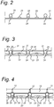
- Figure 2 shows a cross-section of the back-contacted solar panel during a first manufacturing step.
- figure 2 corresponds with line II - II in figure 1b .
- the patterned conductive areas 24, 23 are arranged on the polymer layer 21 of the back sheet contact layer 20, the patterned conductive areas 24, 23 are arranged.
- the conductive areas with reference 24 are interconnected and should connect to electrical contacts of one polarity on the at least one back-contacted solar cell 10. Therefore, interconnecting bodies 25 are put on the conductive areas 24 for providing (at later stage of the manufacturing process) electrical connection between the conductive areas 24 of the conductor circuit and the electrical contact 13 of the back-contacted solar cell(s) 10.
- the interconnecting bodies 25 may be embodied as dots of a conductive adhesive or dots of a conductive polymer or dots of a hybrid material containing solder and a polymer, as preforms of a conductive polymer or preforms of a hybrid material containing solder and a polymer, as parts cut or stamped from a conductive tape.
- the material of the interconnecting bodies is stencil printed on the back-sheet contact layer by depositing a dot of the material at each of the locations corresponding to the electrical contacts of the one or more solar cells.
- the shape and size of the dot is predetermined by the thickness of the stencil and the size of the interconnecting body to be formed.
- the height of the dot is typically at least 125% of the thickness of the encapsulant layer used (see below).
- interconnecting bodies 25 will be put on the other conductive area 23 at locations corresponding with locations of the electrical contacts 12 of the opposite polarity on the rear surface 11 of the back-contacted solar cell(s).
- the material of the interconnecting body is a conductive adhesive.
- the conductive adhesive is a composite with a matrix material based on a polymer selected from a group of epoxy, silicone, acrylate and hybrid polymers and comprises a conductive component.
- the conductive adhesive comprises metal particles forming a conductive path as the conductive component.
- the conductive adhesive comprises low temperature solder as the conductive component that forms a conductive path through the interconnecting body.
- Figure 3 shows a cross-section of the back-contacted solar panel during a subsequent manufacturing step.
- a first encapsulant layer 30 will be arranged over the arrangement of the back sheet contact layer 20 and the interconnecting bodies 25 positioned thereon.
- This first encapsulant layer will serve as an insulating layer between the conductor circuit and the rear surface of the solar cell(s). Also, the first encapsulant layer will serve as a sealing layer to protect the solar cells from moisture etc.
- the first encapsulant layer 30 is provided with a plurality of openings 31 that correspond with the locations of the interconnecting bodies 25 and the locations of the electrical contacts on the rear surface of the back-contacted solar cell.
- the first encapsulant layer has such a thickness that the interconnecting bodies 25 protrude above the top surface 30a of the encapsulant layer 30.
- the first encapsulant layer comprises a polymer preferably a thermoplastic polymer.
- the first encapsulant layer comprises a polymer selected from a group comprising ethylene-vinyl-acetate, ionomers, silicone based encapsulants, TPU (thermoplastic urethane), PVB (polyvinyl butyral).
- Figure 4 shows a cross-section of the back-contacted solar panel during a next manufacturing step.
- the back-contacted solar cell(s) are positioned on top of the interconnecting bodies and the top surface of the first encapsulant layer.
- the electrical contacts 12, 13 on the rear surface of each solar cell 10 are positioned at the locations of the corresponding protruding interconnecting bodies 25.
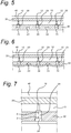
- Figure 5 shows a cross-section of the back-contacted solar panel during yet a further manufacturing step.
- a second encapsulant layer 35 is positioned over the front surfaces of the solar cells 10.
- the second encapsulant layer serves the purpose to electrically insulate the solar cells, to provide an elastic layer for accommodating the solar cells on the glass plate (see below) and to seal them from harmful substances such as moisture.
- the second encapsulant layer comprises a thermoplastic polymer.
- the second encapsulant layer comprises a polymer selected from a group comprising ethylene-vinyl-acetate, ionomers, (poly) silicone based encapsulants, TPU, and PVB.
- a glass plate 40 is arranged on top of the second encapsulant layer 35.
- the solar panel comprises a stacked structure of the back sheet contact layer 20 with a conductor circuit 21, the first encapsulant layer 30 with interconnecting bodies 25 in openings of the first encapsulant layer, the solar cell(s) 10, the second encapsulant layer 35 and the glass plate 40.
- the stacked structure may be inverted so that during processing of the panel, the glass sheet is on the bottom of the stack.
- the stacked structure is exposed to elevated temperature and elevated pressure during a lamination process.
- a lamination process takes place in a laminator device (not shown), curing both the encapsulant layers and the interconnecting body material so as to form a continuous laminate.
- the interaction of the various materials i.e., the encapsulant material and the material of the interconnection is critical in obtaining a compressive stress to reinforce the interconnection.
- the temperature profile of the combined lamination and interconnection step is divided into three stages.
- the first stage heats the laminate from room temperature to approximately 150°C over a period of approximately 5 minutes.
- the double vacuum chamber above the laminate is evacuated.
- pressure is applied to the laminate by allowing the top chamber of the laminator to return to atmospheric pressure.
- the laminate is held at 150°C with the vacuum in the lower chamber being maintained for a period of approximately 15 minutes.
- the final stage comprises the steps to break the vacuum, remove the laminate from the laminator and to allow it to cool to room temperature.
- the interconnection dot (or paste) must either start to cure or be able to maintain its height as determined by the printing step.
- the interconnecting material has been cured or starts curing before the flow and shrinkage of the encapsulant material(s) takes place.
- an onset temperature for the curing of the interconnecting material is lower than an onset temperature for the flow of the encapsulant material. In this manner, the interconnecting material has started to cure fully or to large extent, when the flow of the encapsulant material takes place, thus providing mechanical strength to the interconnecting body during the flow of the encapsulant material.
- the encapsulant material will melt and flow to fill any cavities in the module. Adhesion between the back-sheet foil and the encapsulant material and between the glass and encapsulant material is established during this stage. Adhesion between the back-sheet and the encapsulant material will pull the back-sheet towards the other materials making up the laminate. As the interconnection material can maintain its height at this stage, it will not move with the back-sheet, but will resist its movement, resulting in a compressive stress on the interconnection. The interconnection bodies material will either reach complete cure during the second stage or will not show any deformation, but at the same time will be capable of forming an adhesive bond with and electric contact between the electrical contacts of the cells and the contact area of the conductive back-sheet. At the end of this stage, the laminate will have reached a steady state with good adhesion between all relevant surfaces and a stable electrical contact between the cells and the conductive back-sheet.
- the encapsulant layers 30 shrink to some extent in a direction perpendicular to the interface between the respective encapsulant layer and the surface of the solar cell.
- the laminate will cool to room temperature.
- the coefficient of thermal expansion of the first encapsulant is typically 4 to 5 times higher than that of the conductive adhesive. This implies that the change in height of the encapsulant (i.e. perpendicular to its interface with solar cell) and will be greater than the change in height of the conductive adhesive in the same direction. This difference in change in height will result in an extra compressive stress being imposed on the conductive adhesive by the conductive back-sheet which has become attached to the encapsulant during the encapsulation process.
- a combination of interconnecting material and encapsulant material is selected that produces after the lamination process and cooling a compressive stress in the interconnecting material.
- the interconnecting bodies are under a compressive stress.
- the compressive stress may be due to the occurrence of a difference in volume of the respective layers during the lamination process, with a volume of the encapsulant material being relatively smaller than the volume of the interconnecting material after the lamination process.
- the difference in volume may be brought about by either chemical or physical effects (a chemical reaction or a change of density for example) in the respective layer.
- the volume of the interconnecting body is selected to be larger than the volume of the encapsulant layer, without taking into account an thermal effects: the dots that are stencil printed are protruding from the openings in the encapsulant layer, i.e., are relatively oversized and have a height larger than the thickness of the encapsulant layer.
- the back-sheet layer and the encapsulant layer are made to press on the interconnecting body material due to the volume difference, causing a compressive stress in the interconnecting bodies.
- the combination of interconnecting material and encapsulant material is selected such that due to the lamination process the interconnecting material shrinks relatively less than the encapsulant layer material, which has also the effect that the interconnecting bodies are pressed between the solar cell surface and the encapsulant layer and are in a state of compressive stress.
- the method can apply only the shrinkage effect but may combine this shrinkage effect with the effect caused by the oversize effect.
- the combination of interconnecting material and encapsulant material is selected such that the interconnecting body material has a relatively smaller thermal expansion coefficient than the thermal expansion coefficient of the encapsulant material.
- this has the effect that due to the lamination process the interconnecting material shows a thermal shrinkage that is relatively less than the thermal shrinkage of the encapsulant layer material.
- This has also the effect that the interconnecting bodies are pressed between the solar cell surface and the encapsulant layer and are in a state of compressive stress.
- the method can apply only the thermal shrinkage effect but may combine this thermal shrinkage effect with the effect caused by either the shrinkage effect or the oversize effect, or their combination.
- the interconnecting bodies will be exposed to a compressive force by the surrounding encapsulant layer material. If the material of the interconnecting bodies is strong enough to withstand the compressive force imposed on it by the back-sheet and encapsulant, the interconnecting bodies are able to form a good and reliable interconnection in a back-contact module.
- the shrinkage of the encapsulant layers is resisted by the glass sheet, so causing the encapsulant and back-sheet contact layers to impose a compressive force on the interconnecting bodies between the conductor circuit on the back-sheet contact layer and the rear surface of the solar cells.
- the interconnection does not rely solely on the adhesive strength of the interconnection material with the cell contact pad and the conductive back-sheet, but is reinforced by a compressive force imposed by the encapsulant and back-sheet.
- a solar panel is provided with a stack comprising at least one solar cell, a first encapsulant layer and a back-sheet contact layer; the at least one solar cell being arranged as a back contacted solar cell with a front surface for receiving radiation and a rear surface provided with electrical contacts; the back contact sheet layer having a surface provided with a patterned conductor circuit, the conductor circuit being arranged with contacting areas located at locations corresponding to locations of the electrical contacts on the at least one solar cell; the first encapsulant layer being provided with a pattern of openings at locations corresponding to the locations of the electrical contacts on the at least one solar cell; the at least one solar cell being arranged on top of the first encapsulant layer; the first encapsulant layer being arranged on top of the back-sheet contact layer, with the rear surface of the at least one solar cell facing the patterned conductor circuit surface, such that the first encapsulant layer is between the at least one solar cell and the back-sheet contact layer; the locations of the electrical contacts, the openings
- Figure 6 shows a cross-section of a solar panel according to the invention, wherein the compression of the interconnecting bodies is observable by bulges in the back-sheet contact layer at locations corresponding with the locations of the interconnecting bodies in the solar panel.
- Figure 7 shows a detail of the cross-section of a solar panel according to the invention.
- the compressive force indicates that the interconnecting body is in fact pressed between the interfaces with the electrical contact 12; 13 and the contacting area of the conductor circuit, respectively.
- the pressure on the interfaces ensures that a good contact is maintained.
- the compressive force on the interconnecting body may be balanced by a tensile force on the shrunk encapsulant layers.
- the shrinkage of the encapsulant layer material and of the interconnecting body material can be of a chemical or physical nature, e.g., a change of composition, or density, or difference in thermal expansion or flow between the respective materials.
- shrinkage is defined here as an effective change of volume of the respective material.
- the material of the interconnecting body has a smaller overall shrinkage than an overall shrinkage of the material of the first encapsulant layer during the lamination process.
- the material of the interconnecting body has a smaller thermal shrinkage than a thermal shrinkage of a material of the first encapsulant layer in a temperature interval from a lamination temperature to about room temperature.
- the lamination temperature could be a temperature in a range between about 150 and about 100 °C.
- the manufacturing steps can be defined by a method for manufacturing a solar panel comprising a stack of at least one solar cell, a back-sheet contact layer and a first encapsulant layer, comprising the steps of:
Landscapes
- Photovoltaic Devices (AREA)
- Engineering & Computer Science (AREA)
- Life Sciences & Earth Sciences (AREA)
- Sustainable Development (AREA)
- Sustainable Energy (AREA)
- Adhesives Or Adhesive Processes (AREA)
- Manufacturing & Machinery (AREA)
- Microelectronics & Electronic Packaging (AREA)
Description
- The present invention relates to a solar panel and to a method for manufacturing such a solar panel.
- Back-contacted solar panels or photovoltaic (PV) modules are well known in the art.
- Within the solar panel an array of back-contacted solar cells is arranged. Back-contacted cells are typically interconnected using either short tabs attached to bus-bars at the edges of the rear of the cell or using a conductive back-sheet foil.
- The former method of using short tabs involves soldering the tabs to the contact points on the cell. This results in local residual stress on one side of the cell. This is seen in bowing and in some cases cracking of the cells. During lamination, the cells are flattened so increasing the chance of damage and power loss. Cracks will also grow during the operation of the module further reducing power output.
- The latter method of using a conductive back-sheet foil relates to a module technology based on a patterned conductive back-sheet foil for this type of cell. The pattern on the foil matches the contact points on the cell resulting in a series connection of the cells in the module. Interconnection between the cell and the foil can be done using solder or another type of conductive paste. Soldered modules are typically manufactured by using in-laminate soldering which involves the use of local heating of solder bumps by laser. Modules of this type typically show good performance in damp-heat, but poorer performance in thermal cycling showing that the adhesion strength between the solder, the cell and foil were insufficient.
- "Single-step laminated full-size PV modules made with back-contacted MC-Si cells and conductive adhesives" by P.C. de Jong et al., 19th European Photovoltaic Solar Energy Conference, Paris 7-11 June 2004 , pp. 2145-2148, discloses a method for creating solar panel modules with back contacted PV cells using electrically conductive adhesives using a back-sheet foil that has been modified into an interconnection foil.
- The method is arranged such that the mechanical strength of the adhesive is large enough to handle the mechanical shear stresses seen at the interconnection joints during temperature cycling and withstand tearing of the adhesive due to the shear stresses. It is observed that "bad" connections are formed due to too fast curing of the encapsulant layer.
- "First experiments on module assembly line using back-contact solar cells" by M. Späth et al., 23rd European Photovoltaic Solar Energy Conference, 1-5 September 2008, Valencia, Spain, pp. 2917-2921, discloses a method for creating solar panel modules with "ultra -thin" (130µm) back contacted PV cells by using interconnecting adhesives instead of soldered contacts to overcome large shear stresses at the interface between solar cell and interconnecting body and/or the interface between back sheet and interconnecting body.
- It is an object of the present invention to provide a solar panel which overcomes the disadvantages from the prior art.
- Additionally, it is an object of the invention to provide a method for manufacturing such a solar panel.
- The object is achieved by a solar panel provided with a stack comprising at least one solar cell, a first encapsulant layer and a back-sheet contact layer; the at least one solar cell being arranged as a back contacted solar cell with a front surface for receiving radiation and a rear surface provided with electrical contacts; the back contact sheet layer having a surface provided with a patterned conductor circuit, the conductor circuit being arranged with contacting areas located at locations corresponding to locations of the electrical contacts on the at least one solar cell; the first encapsulant layer being provided with a pattern of openings at locations corresponding to the locations of the electrical contacts on the at least one solar cell; the at least one solar cell being arranged on top of the first encapsulant layer; the first encapsulant layer being arranged on top of the back-sheet contact layer, with the rear surface of the at least one solar cell facing the patterned conductor circuit surface, such that the first encapsulant layer is between the at least one solar cell and the back-sheet contact layer; the locations of the electrical contacts, the openings in the first encapsulant layer and the contacting areas being aligned with each other; each electrical contact of the at least one solar cell being connected through a corresponding opening in the first encapsulant layer with a respective corresponding contacting area of the conductor circuit by an interconnecting body, the interconnecting body being arranged in the opening in the first encapsulant layer, wherein the interconnecting body in a cured state is compressed between the contacting area and the corresponding electrical contact in such a way that in a direction perpendicular to an interface of the solar cell and the first encapsulant layer, the interconnecting body is in a pre-stressed state of a compressive stress.
- Advantageously, the difference in (thermal) shrinkage provides that at low temperature (say about room temperature or lower, for example at night or under cloudy skies) the interconnecting body is compressed between the contact area of the conductor circuit and the electrical contact of the solar cell. This results in a pre-stressed state of the interconnecting body that counteracts the expansion during the heating step of a thermal cycle, for example, during daytime exposure to sunlight. In this manner, the interconnection between the back-sheet contact layer and the solar cell contacts is strengthened.
- According to an aspect of the invention, there is provided a solar panel as described above wherein the material of the interconnecting body has a smaller thermal shrinkage than a thermal shrinkage of a material of the first encapsulant layer during lamination in a temperature interval from an elevated lamination temperature to about room temperature. If the interconnecting body shows less thermal shrinkage than the first encapsulant layer material the first encapsulant layer will compress the interconnecting bodies in the openings of the first encapsulant layer.
- According to an aspect of the invention, there is provided a solar panel as described above wherein a material of the interconnecting body has a smaller overall shrinkage than an overall shrinkage of a material of the first encapsulant layer during the lamination process.
- If the interconnecting body shows less overall shrinkage than the first encapsulant layer material the first encapsulant layer will compress the interconnecting bodies in the openings of the first encapsulant layer.
- According to an aspect of the invention, there is provided a solar panel as described above wherein the material of the interconnecting body has an effective thermal expansion coefficient smaller that the effective thermal expansion coefficient of the material of the first encapsulant layer in said temperature interval.
- According to an aspect of the invention, there is provided a solar panel as described above wherein the material of the interconnecting body has a smaller thermal shrinkage than the thermal shrinkage of the material of the back-sheet contact layer in said temperature interval.
- The back-sheet contact layer can thus produce additional compression on the interconnecting bodies.
- According to an aspect of the invention, there is provided a solar panel as described above, wherein the thermal shrinkage is determined substantially perpendicular to the interface of the first encapsulant layer and the solar cell.
- If the compressive stress is mainly directed perpendicular to the interface, the connection between the conductor circuit contacting area and the corresponding solar cell contact is improved.
- According to an aspect of the invention, there is provided a solar panel as described above, wherein the material of the interconnecting body is a conductive adhesive.
- Advantageously, this interconnecting body material can be easily applied on the conductor area contacting areas. Also, this type of material can be tuned to have appropriate curing characteristics and mechanical properties to obtain interconnecting bodies showing compressive stress after lamination process.
- According to an aspect of the invention, there is provided a solar panel as described above, wherein the conductive adhesive is a composite with a matrix material based on a polymer selected from a group of epoxy, acrylate, and silicone, and comprising a conductive component.
- According to an aspect of the invention, there is provided a solar panel as described above wherein the conductive adhesive comprises metal particles forming a conductive path as the conductive component.
- The conductive adhesive may be mixed with metallic particles that form conductive paths in the interconnecting bodies.
- According to an aspect of the invention, there is provided a solar panel as described above wherein the conductive adhesive comprises as the conductive component a conductive path(s) consisting of low temperature solder.
- The conductive adhesive may be mixed with low temperature solder material that may flow and form a conductive path(s) in the interconnecting bodies
- According to an aspect of the invention, there is provided a solar panel as described above, wherein the solar panel further comprises a second encapsulant layer and a glass plate; the second encapsulant layer being arranged on top of the front surface of the at least one solar cell, and the glass plate being on top of the second encapsulant layer, the second encapsulant layer thus being between the at least one solar cell and the glass plate.
- According to an aspect of the invention, there is provided a solar panel as described above, wherein the first and/or second encapsulant layer comprises a polymer selected from a group comprising ethylene-vinyl-acetate, ionomers, (poly)silicone, thermoplastic urethane, and polyvinyl butyral.
- Such polymers show good properties of flow and shrinkage during the lamination process.
- According to an aspect of the invention, there is provided a solar panel as described above, wherein the at least one solar cell is a silicon based back-contacted solar cell.
- According to an aspect of the invention, there is provided a solar panel as described above, wherein in the back-sheet contact layer bulges are observable at locations corresponding with the locations of the interconnecting bodies in the solar panel.
- Moreover, the present invention provides a method for manufacturing a solar panel as described above, the method comprising the steps of:
- -- providing one or more back contacted solar cells with a front surface for receiving radiation and a rear surface provided with electrical contacts as the at least one solar cell;
- -- providing the back-sheet contact layer with a patterned conductor circuit on a surface thereof, the conductor circuit being arranged with contacting areas located at locations corresponding to locations of the electrical contacts on the at least one solar cell;
- -- providing at each contacting area an interconnecting body;
- -- providing the first encapsulant layer with a pattern of openings at locations corresponding to the locations of the electrical contacts on the at least one solar cell;
- -- arranging the patterned first encapsulant layer on top of the back-sheet contact layer, the pattern of openings being aligned with the locations of the electrical contacts in such a way that each interconnecting body is located in the corresponding opening in the first encapsulant layer;
- -- arranging the at least one solar cell on top of the patterned first encapsulant layer with the rear surface of the at least one solar cell facing the patterned conductor circuit surface, and each of the electrical contacts of the at least one solar cell faces the corresponding interconnection body through the first encapsulant layer;
- -- connecting each electrical contact of the at least one solar cell with a respective corresponding contacting area of the conductor circuit by the corresponding interconnecting body in the respective corresponding opening in the first encapsulant layer;
- -- creating during a lamination step a compressive stress in the interconnecting body in a direction perpendicular to an interface between the at least one solar cell and the first encapsulant layer,
- According to an aspect of the invention, there is provided a method as described above, wherein the material of the interconnecting body has a smaller overall shrinkage than an overall shrinkage of the material of the first encapsulant layer during the lamination process.
- According to an aspect of the invention, there is provided a method as described above, wherein the material of the interconnecting body has a smaller thermal shrinkage than a thermal shrinkage of a material of the first encapsulant layer during lamination in a temperature interval from an elevated lamination temperature to about room temperature.
- According to an aspect of the invention, there is provided a method as described above, wherein each interconnecting body is formed as a dot on the corresponding contacting area of the conductor circuit by stencil printing preceding the step of arranging the patterned first encapsulant layer on top of the back-sheet contact layer.
- According to an aspect of the invention, there is provided a method as described above, wherein the formation of the dot includes that the formed dot has a height substantially larger than a thickness of the patterned first encapsulant layer.
- According to an aspect of the invention, there is provided a method as described above, wherein the at least one solar cell is arranged on the patterned first encapsulant layer after formation of the interconnecting body dots on the contacting areas of the conductor circuit.
- According to an aspect of the invention, there is provided a method as described above, wherein the material of the interconnecting body is a conductive adhesive and said step of connecting each electrical contact of the at least one solar cell with a respective corresponding contacting area of the conductor circuit comprises a curing heat treatment of the interconnecting body dot to form the interconnecting body.
- According to an aspect of the invention, there is provided a method as described above, further comprising:
- -- providing a second encapsulant layer over the front surface of the at least one solar cell;
- -- providing a glass plate over the second encapsulant layer;
- -- laminating the stack comprising the back-sheet contact layer, the first encapsulant layer, the at least one solar cell, the second encapsulant layer and the glass plate by exposure to an elevated temperature and an elevated pressure to form the solar panel.
- According to an aspect of the invention, there is provided a method as described above, wherein the curing heat treatment of the interconnecting body dots takes place during said lamination step.
- According to an aspect of the invention, there is provided a method as described above, wherein before said lamination step the first encapsulant layer has a thickness smaller than a height of the interconnection body.
- The invention will be explained in more detail below with reference to drawings in which illustrative embodiments of the invention are shown. The drawings are intended for illustration purposes only without limitation of the scope of protection which is defined by the subject matter of the appended claims.
-
-
Figure 1a shows schematically a layout of a rear surface of back-contacted solar cells for application in a back contact solar panel; -
Figure 1b shows schematically a layout of a conductor circuit on a back-sheet contact layer corresponding with the layout of contacts of the back-contacted solar cells ofFigure 1a ; -
Figure 2 shows a cross-section of the back-contacted solar panel during a first manufacturing step; -
Figure 3 shows a cross-section of the back-contacted solar panel during a subsequent manufacturing step; -
Figure 4 shows a cross-section of the back-contacted solar panel during a next manufacturing step; -
Figure 5 shows a cross-section of the back-contacted solar panel during yet a further manufacturing step according to an embodiment of the invention; -
Figure 6 shows a cross-section of the back-contacted solar panel according to an embodiment of the invention; -
Figure 7 shows a detail of the cross-section of a solar panel according to the invention. -
Figure 1a shows schematically a layout of a rear surface of back-contacted solar cells for application in a back contact solar panel. - Solar cells are typically provided with a pattern of conductive lines to carry electric charge that is generated by the photovoltaic effect in the solar cell. Various types of solid state solar cells are available, based on substrates of various semiconductor materials, for example, poly- or monocrystalline silicon.
- In back-contacted solar cells the contacts of the conductor pattern are arranged on a rear surface of the solar cell, so as to minimize shadow losses on the front surface of the solar cell that faces in use a radiation source for example the Sun.
- In
figure 1a , a layout of an array of two back-contacted solar cells, adjacent to each other is shown. On eachsolar cell 10, a plurality of contacts of bothpolarities 12, 13 (e.g.,positive contacts 12 and negative contacts 13) is arranged on therear surface 11 of the solar cell. - The solar cells may be of the MWT (metal-wrap-through), EWT (Emitter wrap-through), IBC (interdigitated back-contact) or other back-contact silicon substrate type, that comprise all contacts at the rear of the cell either by conductive vias through the silicon substrate to connect the front surface region with rear surface electrical contact(s) of the solar cell or by having both the p- and n-type junctions and electrical contact(s) at the rear of the solar cell.
-
Figure 1b shows schematically a layout of a conductor circuit on a back-sheet contact layer corresponding with the layout of electrical contacts of the back-contacted solar cells ofFigure 1a . - The back-
sheet contact layer 20 is typically a polymer basedlayer 21 provided with a patterned conductive layer, i.e., a conductor circuit comprising one or more patternedconductive areas - The layout of the conductor circuit matches substantially the layout of the
electrical contacts rear surface 11 of the back-contactedsolar cells 10 and with the arrangement of thesolar cells 10 next to each other. - In
figure 1b the locations where the conductor circuit is to be in electrical contact with theelectrical contacts 12; 13 of the at least one back-contactedsolar cell 10 are indicated by crosses 28. -
Figure 2 shows a cross-section of the back-contacted solar panel during a first manufacturing step. - The cross-section of
figure 2 corresponds with line II - II infigure 1b . - On the
polymer layer 21 of the backsheet contact layer 20, the patternedconductive areas reference 24 are interconnected and should connect to electrical contacts of one polarity on the at least one back-contactedsolar cell 10. Therefore, interconnectingbodies 25 are put on theconductive areas 24 for providing (at later stage of the manufacturing process) electrical connection between theconductive areas 24 of the conductor circuit and theelectrical contact 13 of the back-contacted solar cell(s) 10. - The interconnecting
bodies 25 may be embodied as dots of a conductive adhesive or dots of a conductive polymer or dots of a hybrid material containing solder and a polymer, as preforms of a conductive polymer or preforms of a hybrid material containing solder and a polymer, as parts cut or stamped from a conductive tape. - In an embodiment, the material of the interconnecting bodies is stencil printed on the back-sheet contact layer by depositing a dot of the material at each of the locations corresponding to the electrical contacts of the one or more solar cells. The shape and size of the dot is predetermined by the thickness of the stencil and the size of the interconnecting body to be formed. The height of the dot is typically at least 125% of the thickness of the encapsulant layer used (see below).
- In a similar way, interconnecting
bodies 25 will be put on the otherconductive area 23 at locations corresponding with locations of theelectrical contacts 12 of the opposite polarity on therear surface 11 of the back-contacted solar cell(s). - In an embodiment, the material of the interconnecting body is a conductive adhesive.
- In a further embodiment, the conductive adhesive is a composite with a matrix material based on a polymer selected from a group of epoxy, silicone, acrylate and hybrid polymers and comprises a conductive component.
- In an embodiment, the conductive adhesive comprises metal particles forming a conductive path as the conductive component.
- Alternatively, the conductive adhesive comprises low temperature solder as the conductive component that forms a conductive path through the interconnecting body.
-
Figure 3 shows a cross-section of the back-contacted solar panel during a subsequent manufacturing step. - In a subsequent manufacturing step, a
first encapsulant layer 30 will be arranged over the arrangement of the backsheet contact layer 20 and the interconnectingbodies 25 positioned thereon. This first encapsulant layer will serve as an insulating layer between the conductor circuit and the rear surface of the solar cell(s). Also, the first encapsulant layer will serve as a sealing layer to protect the solar cells from moisture etc. - The
first encapsulant layer 30 is provided with a plurality ofopenings 31 that correspond with the locations of the interconnectingbodies 25 and the locations of the electrical contacts on the rear surface of the back-contacted solar cell. - The first encapsulant layer has such a thickness that the interconnecting
bodies 25 protrude above thetop surface 30a of theencapsulant layer 30. - In an embodiment, the first encapsulant layer comprises a polymer preferably a thermoplastic polymer. In an embodiment, the first encapsulant layer comprises a polymer selected from a group comprising ethylene-vinyl-acetate, ionomers, silicone based encapsulants, TPU (thermoplastic urethane), PVB (polyvinyl butyral).
-
Figure 4 shows a cross-section of the back-contacted solar panel during a next manufacturing step. - In this manufacturing step, the back-contacted solar cell(s) are positioned on top of the interconnecting bodies and the top surface of the first encapsulant layer. The
electrical contacts solar cell 10 are positioned at the locations of the corresponding protruding interconnectingbodies 25. -
Figure 5 shows a cross-section of the back-contacted solar panel during yet a further manufacturing step. - During this manufacturing step, a
second encapsulant layer 35 is positioned over the front surfaces of thesolar cells 10. The second encapsulant layer serves the purpose to electrically insulate the solar cells, to provide an elastic layer for accommodating the solar cells on the glass plate (see below) and to seal them from harmful substances such as moisture. - In an embodiment, the second encapsulant layer comprises a thermoplastic polymer. In an embodiment, the second encapsulant layer comprises a polymer selected from a group comprising ethylene-vinyl-acetate, ionomers, (poly) silicone based encapsulants, TPU, and PVB.
- After placing the second encapsulant layer, a
glass plate 40 is arranged on top of thesecond encapsulant layer 35. - After these steps, the solar panel comprises a stacked structure of the back
sheet contact layer 20 with aconductor circuit 21, thefirst encapsulant layer 30 with interconnectingbodies 25 in openings of the first encapsulant layer, the solar cell(s) 10, thesecond encapsulant layer 35 and theglass plate 40. - The stacked structure may be inverted so that during processing of the panel, the glass sheet is on the bottom of the stack.
- Subsequently, the stacked structure is exposed to elevated temperature and elevated pressure during a lamination process. Such lamination process takes place in a laminator device (not shown), curing both the encapsulant layers and the interconnecting body material so as to form a continuous laminate.
- During the combined lamination and interconnection step in module manufacturing using back-contact cells with a conductive back-sheet and interconnection paste, the interaction of the various materials i.e., the encapsulant material and the material of the interconnection, is critical in obtaining a compressive stress to reinforce the interconnection.
- The temperature profile of the combined lamination and interconnection step is divided into three stages. The first stage heats the laminate from room temperature to approximately 150°C over a period of approximately 5 minutes. During the first part of this stage, the double vacuum chamber above the laminate is evacuated. When the temperature is above approximately 80°C, pressure is applied to the laminate by allowing the top chamber of the laminator to return to atmospheric pressure. In the second stage, the laminate is held at 150°C with the vacuum in the lower chamber being maintained for a period of approximately 15 minutes. The final stage comprises the steps to break the vacuum, remove the laminate from the laminator and to allow it to cool to room temperature.
- During the first stage, the interconnection dot (or paste) must either start to cure or be able to maintain its height as determined by the printing step.
- Preferably, the interconnecting material has been cured or starts curing before the flow and shrinkage of the encapsulant material(s) takes place. In an embodiment, an onset temperature for the curing of the interconnecting material is lower than an onset temperature for the flow of the encapsulant material. In this manner, the interconnecting material has started to cure fully or to large extent, when the flow of the encapsulant material takes place, thus providing mechanical strength to the interconnecting body during the flow of the encapsulant material.
- During the second stage, the encapsulant material will melt and flow to fill any cavities in the module. Adhesion between the back-sheet foil and the encapsulant material and between the glass and encapsulant material is established during this stage. Adhesion between the back-sheet and the encapsulant material will pull the back-sheet towards the other materials making up the laminate. As the interconnection material can maintain its height at this stage, it will not move with the back-sheet, but will resist its movement, resulting in a compressive stress on the interconnection. The interconnection bodies material will either reach complete cure during the second stage or will not show any deformation, but at the same time will be capable of forming an adhesive bond with and electric contact between the electrical contacts of the cells and the contact area of the conductive back-sheet. At the end of this stage, the laminate will have reached a steady state with good adhesion between all relevant surfaces and a stable electrical contact between the cells and the conductive back-sheet.
- During lamination including the cooling step afterwards, the encapsulant layers 30 (and the back-sheet contact layer) shrink to some extent in a direction perpendicular to the interface between the respective encapsulant layer and the surface of the solar cell.
- During the final stage of lamination, the laminate will cool to room temperature.
- According to an aspect of the invention, the coefficient of thermal expansion of the first encapsulant is typically 4 to 5 times higher than that of the conductive adhesive. This implies that the change in height of the encapsulant (i.e. perpendicular to its interface with solar cell) and will be greater than the change in height of the conductive adhesive in the same direction. This difference in change in height will result in an extra compressive stress being imposed on the conductive adhesive by the conductive back-sheet which has become attached to the encapsulant during the encapsulation process.
- Thus, according to the invention a combination of interconnecting material and encapsulant material is selected that produces after the lamination process and cooling a compressive stress in the interconnecting material.
- In the solar panel in a direction perpendicular to an interface of the solar cell and the first encapsulant layer, the interconnecting bodies are under a compressive stress.
- The compressive stress may be due to the occurrence of a difference in volume of the respective layers during the lamination process, with a volume of the encapsulant material being relatively smaller than the volume of the interconnecting material after the lamination process.
- The difference in volume may be brought about by either chemical or physical effects (a chemical reaction or a change of density for example) in the respective layer.
- In an embodiment, the volume of the interconnecting body is selected to be larger than the volume of the encapsulant layer, without taking into account an thermal effects: the dots that are stencil printed are protruding from the openings in the encapsulant layer, i.e., are relatively oversized and have a height larger than the thickness of the encapsulant layer. During lamination the back-sheet layer and the encapsulant layer are made to press on the interconnecting body material due to the volume difference, causing a compressive stress in the interconnecting bodies.
- Additionally or alternatively, the combination of interconnecting material and encapsulant material is selected such that due to the lamination process the interconnecting material shrinks relatively less than the encapsulant layer material, which has also the effect that the interconnecting bodies are pressed between the solar cell surface and the encapsulant layer and are in a state of compressive stress. The method can apply only the shrinkage effect but may combine this shrinkage effect with the effect caused by the oversize effect.
- Additionally or alternatively, the combination of interconnecting material and encapsulant material is selected such that the interconnecting body material has a relatively smaller thermal expansion coefficient than the thermal expansion coefficient of the encapsulant material. Again, this has the effect that due to the lamination process the interconnecting material shows a thermal shrinkage that is relatively less than the thermal shrinkage of the encapsulant layer material. This has also the effect that the interconnecting bodies are pressed between the solar cell surface and the encapsulant layer and are in a state of compressive stress. The method can apply only the thermal shrinkage effect but may combine this thermal shrinkage effect with the effect caused by either the shrinkage effect or the oversize effect, or their combination.
- It has been found that if the
interconnection body material 25 does not shrink or shrinks less than the encapsulant layer material during the combined lamination and interconnection step, the interconnecting bodies will be exposed to a compressive force by the surrounding encapsulant layer material. If the material of the interconnecting bodies is strong enough to withstand the compressive force imposed on it by the back-sheet and encapsulant, the interconnecting bodies are able to form a good and reliable interconnection in a back-contact module. - The shrinkage of the encapsulant layers is resisted by the glass sheet, so causing the encapsulant and back-sheet contact layers to impose a compressive force on the interconnecting bodies between the conductor circuit on the back-sheet contact layer and the rear surface of the solar cells.
- In doing this, the interconnection does not rely solely on the adhesive strength of the interconnection material with the cell contact pad and the conductive back-sheet, but is reinforced by a compressive force imposed by the encapsulant and back-sheet.
- Thus according to the invention, a solar panel is provided with a stack comprising at least one solar cell, a first encapsulant layer and a back-sheet contact layer; the at least one solar cell being arranged as a back contacted solar cell with a front surface for receiving radiation and a rear surface provided with electrical contacts; the back contact sheet layer having a surface provided with a patterned conductor circuit, the conductor circuit being arranged with contacting areas located at locations corresponding to locations of the electrical contacts on the at least one solar cell; the first encapsulant layer being provided with a pattern of openings at locations corresponding to the locations of the electrical contacts on the at least one solar cell; the at least one solar cell being arranged on top of the first encapsulant layer; the first encapsulant layer being arranged on top of the back-sheet contact layer, with the rear surface of the at least one solar cell facing the patterned conductor circuit surface, such that the first encapsulant layer is between the at least one solar cell and the back-sheet contact layer; the locations of the electrical contacts, the openings in the first encapsulant layer and the contacting areas being aligned with each other; each electrical contact of the at least one solar cell being connected through a corresponding opening in the first encapsulant layer with a respective corresponding contacting area of the conductor circuit by an interconnecting body; wherein in a direction perpendicular to an interface of the solar cell and the first encapsulant layer, the interconnecting body is under a compressive stress.
-
Figure 6 shows a cross-section of a solar panel according to the invention, wherein the compression of the interconnecting bodies is observable by bulges in the back-sheet contact layer at locations corresponding with the locations of the interconnecting bodies in the solar panel. -
Figure 7 shows a detail of the cross-section of a solar panel according to the invention. - In this detailed cross-section the compressive force exerted on the interconnecting
body 25 due to the relatively shrunk encapsulant layer material is denoted by the arrows S. - The compressive force indicates that the interconnecting body is in fact pressed between the interfaces with the
electrical contact 12; 13 and the contacting area of the conductor circuit, respectively. The pressure on the interfaces ensures that a good contact is maintained. - The compressive force on the interconnecting body may be balanced by a tensile force on the shrunk encapsulant layers.
- The shrinkage of the encapsulant layer material and of the interconnecting body material can be of a chemical or physical nature, e.g., a change of composition, or density, or difference in thermal expansion or flow between the respective materials.
- Therefore, shrinkage is defined here as an effective change of volume of the respective material.
- In an embodiment, the material of the interconnecting body has a smaller overall shrinkage than an overall shrinkage of the material of the first encapsulant layer during the lamination process.
- Alternatively or additionally, where the shrinkage would be governed by thermal expansion phenomena, the material of the interconnecting body has a smaller thermal shrinkage than a thermal shrinkage of a material of the first encapsulant layer in a temperature interval from a lamination temperature to about room temperature.
- The lamination temperature could be a temperature in a range between about 150 and about 100 °C.
- In an embodiment, the manufacturing steps can be defined by a method for manufacturing a solar panel comprising a stack of at least one solar cell, a back-sheet contact layer and a first encapsulant layer, comprising the steps of:
- -- providing a back contacted solar cell with a front surface for receiving radiation and a rear surface provided with electrical contacts as the at least one solar cell;
- -- providing the back-sheet contact layer with a patterned conductor circuit on a surface thereof, the conductor circuit being arranged with contacting areas located at locations corresponding to locations of the electrical contacts on the at least one solar cell;
- -- providing at each contacting area an interconnecting body;
- -- providing the first encapsulant layer with a pattern of openings at locations corresponding to the locations of the electrical contacts on the at least one solar cell;
- -- arranging the patterned first encapsulant layer on top of the back-sheet contact layer with the pattern of openings aligned over the locations of the electrical contacts in such a way that each interconnecting body is located in the corresponding opening in the first encapsulant layer;
- -- arranging the at least one solar cell on top of the patterned first encapsulant layer with the rear surface of the at least one solar cell facing the patterned conductor circuit surface, and each of the electrical contacts of the at least one solar cell faces the corresponding interconnection body through the first encapsulant layer;
- -- connecting each electrical contact of the at least one solar cell with a respective corresponding contact area of the conductor circuit by the corresponding interconnecting body;
- It will be apparent to the person skilled in the art that other embodiments of the invention can be conceived and reduced to practice without departing from the scope of the invention, the scope of the invention being limited only by the appended claims as finally granted. The description of embodiments above is not intended to limit the scope of the invention.
Claims (21)
- Solar panel provided with a stack comprising at least one solar cell (10), a first encapsulant layer (30) and a back-sheet contact layer (20); the at least one solar cell being arranged as a back contacted solar cell with a front surface for receiving radiation and a rear surface (11) provided with electrical contacts (12, 13); the back contact sheet layer having a surface provided with a patterned conductor circuit (21), the conductor circuit being arranged with contacting areas (22, 23, 24) located at locations corresponding to locations of the electrical contacts on the at least one solar cell;
the first encapsulant layer being provided with a pattern of openings at locations corresponding to the locations of the electrical contacts on the at least one solar cell;
the at least one solar cell being arranged on top of the first encapsulant layer;
the first encapsulant layer being arranged on top of the back-sheet contact layer, with the rear surface of the at least one solar cell facing the patterned conductor circuit surface, such that the first encapsulant layer is between the at least one solar cell and the back-sheet contact layer;
the locations of the electrical contacts, the openings in the first encapsulant layer and the contacting areas being aligned with each other;
each electrical contact of the at least one solar cell being connected through a corresponding opening in the first encapsulant layer with a respective corresponding contacting area of the conductor circuit by an interconnecting body (25), the interconnecting body being arranged in the opening in the first encapsulant layer;
wherein
the material of the interconnecting body is a conductive adhesive; characterized in that the material of the interconnecting body has a smaller thermal shrinkage than a thermal shrinkage of a material of the first encapsulant layer during lamination in a temperature interval from an elevated lamination temperature to about room temperature;
and
the interconnecting body when it has been cured, is compressed between the contacting area and the corresponding electrical contact in such a way that in a direction perpendicular to an interface of the solar cell and the first encapsulant layer, the interconnecting body is pre-stressed under a compressive stress. - Solar panel according to claim 1 wherein a material of the interconnecting body (25) has a smaller overall shrinkage than an overall shrinkage of a material of the first encapsulant layer (30) during the lamination process.
- Solar panel according to claim 1, wherein the material of the interconnecting body (25) has an effective thermal expansion coefficient smaller that the effective thermal expansion coefficient of the material of the first encapsulant layer (30) in said temperature interval.
- Solar panel according to claim 1, wherein the material of the interconnecting body (25) has a smaller thermal shrinkage than the thermal shrinkage of the material of the back-sheet contact layer (20) in said temperature interval.
- Solar panel according to claim 1, wherein the thermal shrinkage is determined substantially perpendicular to the interface of the first encapsulant layer (30) and the solar cell (10).
- Solar panel according to claim 5, wherein the conductive adhesive is a composite with a matrix material based on a polymer selected from a group of epoxy, acrylate, and silicone, and comprising a conductive component.
- Solar panel according to claim 1 or 5, wherein the conductive adhesive comprises metal particles forming a conductive path as the conductive component.
- Solar panel according to claim 1 or claim 5 or claim 6, wherein the conductive adhesive comprises as the conductive component a conductive path consisting of low temperature solder.
- Solar panel according to any one of the preceding claims, wherein the solar panel further comprises a second encapsulant layer (35) and a glass plate (40); the second encapsulant layer being arranged on top of the front surface of the at least one solar cell (10), and the glass plate being on top of the second encapsulant layer, the second encapsulant layer thus being between the at least one solar cell and the glass plate.
- Solar panel according to any one of the preceding claims, wherein the first and/or second encapsulant layer (30, 35) comprises a polymer selected from a group comprising ethylene-vinyl-acetate, ionomers, (poly)silicone, thermoplastic urethane, and polyvinyl butyral.
- Solar panel according to any one of the preceding claims wherein the at least one solar cell (10) is a silicon based back-contacted solar cell.
- Solar panel according to any one of the preceding claims, wherein in the back-sheet contact layer (20) bulges are observable at locations corresponding with the locations of the interconnecting bodies (25) in the solar panel.
- Method for manufacturing a solar panel provided with a stack comprising at least one solar cell (10), a back-sheet contact layer (20) and a first encapsulant layer (30), comprising the steps of:-- providing one or more back contacted solar cells with a front surface for receiving radiation and a rear surface (11) provided with electrical contacts (12, 13) as the at least one solar cell;-- providing the back-sheet contact layer with a patterned conductor circuit (21) on a surface thereof, the conductor circuit being arranged with contacting areas (22, 23, 24) located at locations corresponding to locations of the electrical contacts on the at least one solar cell;-- providing at each contacting area an interconnecting body (25);-- providing the first encapsulant layer with a pattern of openings at locations corresponding to the locations of the electrical contacts on the at least one solar cell;-- arranging the patterned first encapsulant layer on top of the back-sheet contact layer, the pattern of openings being aligned with the locations of the electrical contacts in such a way that each interconnecting body is located in the corresponding opening in the first encapsulant layer;-- arranging the at least one solar cell on top of the patterned first encapsulant layer with the rear surface of the at least one solar cell facing the patterned conductor circuit surface, and each of the electrical contacts of the at least one solar cell faces the corresponding interconnection body through the first encapsulant layer;-- connecting each electrical contact of the at least one solar cell with a respective corresponding contacting area of the conductor circuit by the corresponding interconnecting body in the respective corresponding opening in the first encapsulant layer;-- creating during a lamination step a compressive stress in the interconnecting body in a direction perpendicular to an interface between the at least one solar cell and the first encapsulant layer,wherein the material of the interconnecting body is a conductive adhesive;
wherein the material of the interconnecting body has a smaller thermal shrinkage than a thermal shrinkage of a material of the first encapsulant layer during lamination in a temperature interval from an elevated lamination temperature to about room temperature;
wherein after the lamination process of the stack, the interconnecting body is compressed between the contacting area and the corresponding electrical contact in such a way that in a direction perpendicular to an interface of the solar cell and the first encapsulant layer, the interconnecting body is pre-stressed under a compressive stress. - Method according to claim 13 wherein the material of the interconnecting body (25) has a smaller overall shrinkage than an overall shrinkage of the material of the first encapsulant layer (30) during the lamination process.
- Method according to claim 13 wherein each interconnecting body (25) is formed as a dot on the corresponding contacting area of the conductor circuit (21) by stencil printing preceding the step of arranging the patterned first encapsulant layer (30) on top of the back-sheet contact layer.
- Method according to claim 15, wherein the formation of the dot includes that the formed dot has a height substantially larger than a thickness of the patterned first encapsulant layer (30).
- Method according to claim 15 or 16, wherein the at least one solar cell (10) is arranged on the patterned first encapsulant layer (30) after formation of the interconnecting body dots on the contacting areas of the conductor circuit (21).
- Method according to any one of claims 13 - 17 , wherein the material of the interconnecting body (25) is a conductive adhesive and said step of connecting each electrical contact of the at least one solar cell with a respective corresponding contacting area of the conductor circuit comprises a curing heat treatment of the interconnecting body dot to form the interconnecting body.
- Method according to any one of preceding claims 13 - 18, further comprising:-- providing a second encapsulant layer (35) over the front surface of the at least one solar cell;-- providing a glass plate (40) over the second encapsulant layer;-- laminating the stack comprising the back-sheet contact layer (20), the first encapsulant layer (30), the at least one solar cell (10), the second encapsulant layer and the glass plate by exposure to an elevated temperature and an elevated pressure to form the solar panel.
- Method according to claim 19, wherein the curing heat treatment of the interconnecting body dots takes place during said lamination step.
- Method according to claim 19 or 20, wherein before said lamination step the first encapsulant layer (30) has a thickness smaller than a height of the interconnection body (25).
Applications Claiming Priority (2)
| Application Number | Priority Date | Filing Date | Title |
|---|---|---|---|
| NL2009836A NL2009836C2 (en) | 2012-11-19 | 2012-11-19 | Back-contacted solar panel and method for manufacturing such a solar panel. |
| PCT/NL2013/050819 WO2014077686A1 (en) | 2012-11-19 | 2013-11-14 | Back-contacted solar panel and method for manufacturing such a solar panel |
Publications (2)
| Publication Number | Publication Date |
|---|---|
| EP2920820A1 EP2920820A1 (en) | 2015-09-23 |
| EP2920820B1 true EP2920820B1 (en) | 2018-07-11 |
Family
ID=47360267
Family Applications (1)
| Application Number | Title | Priority Date | Filing Date |
|---|---|---|---|
| EP13801888.2A Not-in-force EP2920820B1 (en) | 2012-11-19 | 2013-11-14 | Back-contacted solar panel and method for manufacturing such a solar panel |
Country Status (8)
| Country | Link |
|---|---|
| US (1) | US20150303342A1 (en) |
| EP (1) | EP2920820B1 (en) |
| JP (1) | JP6366145B2 (en) |
| KR (1) | KR20150088271A (en) |
| CN (1) | CN104885231B (en) |
| NL (1) | NL2009836C2 (en) |
| TW (1) | TWI628807B (en) |
| WO (1) | WO2014077686A1 (en) |
Families Citing this family (9)
| Publication number | Priority date | Publication date | Assignee | Title |
|---|---|---|---|---|
| JP2876738B2 (en) | 1990-07-27 | 1999-03-31 | 株式会社デンソー | Series-parallel switching rotary electric machine |
| KR101658733B1 (en) * | 2015-07-08 | 2016-09-21 | 엘지전자 주식회사 | Solar cell module |
| NL1041939B1 (en) | 2016-06-21 | 2018-01-04 | Petrus Paulus Carolus Maria Stassen Ing | A solar panel and method for increasing safety and reliability of a solar panel |
| AU2020340008B2 (en) * | 2019-08-26 | 2023-06-08 | Longi Solar Technology (Taizhou) Co., Ltd. | Method for producing back-contact solar cell assembly and back-contact solar cell assembly |
| NL2028545B1 (en) | 2021-06-25 | 2023-01-02 | Atlas Technologies Holding Bv | Solar module with improved bonding |
| CN113871491A (en) * | 2021-12-03 | 2021-12-31 | 南京日托光伏新能源有限公司 | A GPS layer and a method for improving the efficiency of a back-contact battery assembly |
| CN114530515A (en) * | 2022-01-27 | 2022-05-24 | 江苏日托光伏科技股份有限公司 | Manufacturing and using method of efficient repairable assembly based on back contact battery |
| CN115172535B (en) * | 2022-09-05 | 2023-01-20 | 晶科能源(海宁)有限公司 | Preparation method of photovoltaic module and photovoltaic module |
| CN221407330U (en) * | 2023-11-14 | 2024-07-23 | 深圳市华宝新能源股份有限公司 | Curved photovoltaic components and photovoltaic building surfaces |
Family Cites Families (10)
| Publication number | Priority date | Publication date | Assignee | Title |
|---|---|---|---|---|
| JPH08298334A (en) * | 1995-04-26 | 1996-11-12 | Mitsubishi Electric Corp | Solar cell plate |
| US6580035B1 (en) * | 1998-04-24 | 2003-06-17 | Amerasia International Technology, Inc. | Flexible adhesive membrane and electronic device employing same |
| US20080236655A1 (en) * | 2007-03-29 | 2008-10-02 | Baldwin Daniel F | Solar module manufacturing processes |
| NL2001958C (en) * | 2008-09-05 | 2010-03-15 | Stichting Energie | Method of monolithic photo-voltaic module assembly. |
| KR101135591B1 (en) * | 2009-03-11 | 2012-04-19 | 엘지전자 주식회사 | Solar cell and solar cell module |
| NL2003936C2 (en) * | 2009-12-10 | 2011-06-14 | Eurotron B V | METHOD AND DEVICE FOR MANUFACTURING SOLAR PANEL USING A CARRIER |
| JP2011138929A (en) * | 2009-12-28 | 2011-07-14 | Sharp Corp | Wiring sheet, solar cell with wiring sheet, solar cell module, and method for manufacturing the wiring sheet and the solar cell module |
| JP4944240B1 (en) * | 2010-11-30 | 2012-05-30 | シャープ株式会社 | Back electrode type solar cell, back electrode type solar cell with wiring sheet, solar cell module, method for manufacturing back electrode type solar cell with wiring sheet, and method for manufacturing solar cell module |
| US20120285501A1 (en) * | 2010-12-29 | 2012-11-15 | E.I. Du Pont De Nemours And Company | Integrated back-sheet for back contact photovoltaic module |
| US8497153B2 (en) * | 2011-10-31 | 2013-07-30 | E I Du Pont De Nemours And Company | Integrated back-sheet for back contact photovoltaic module |
-
2012
- 2012-11-19 NL NL2009836A patent/NL2009836C2/en not_active IP Right Cessation
-
2013
- 2013-11-14 US US14/443,667 patent/US20150303342A1/en not_active Abandoned
- 2013-11-14 WO PCT/NL2013/050819 patent/WO2014077686A1/en not_active Ceased
- 2013-11-14 KR KR1020157015277A patent/KR20150088271A/en not_active Ceased
- 2013-11-14 JP JP2015542989A patent/JP6366145B2/en not_active Expired - Fee Related
- 2013-11-14 CN CN201380060380.1A patent/CN104885231B/en not_active Expired - Fee Related
- 2013-11-14 EP EP13801888.2A patent/EP2920820B1/en not_active Not-in-force
- 2013-11-19 TW TW102141972A patent/TWI628807B/en not_active IP Right Cessation
Non-Patent Citations (1)
| Title |
|---|
| None * |
Also Published As
| Publication number | Publication date |
|---|---|
| NL2009836C2 (en) | 2014-05-21 |
| US20150303342A1 (en) | 2015-10-22 |
| WO2014077686A1 (en) | 2014-05-22 |
| CN104885231A (en) | 2015-09-02 |
| CN104885231B (en) | 2017-03-29 |
| TW201424019A (en) | 2014-06-16 |
| JP2015536571A (en) | 2015-12-21 |
| TWI628807B (en) | 2018-07-01 |
| JP6366145B2 (en) | 2018-08-01 |
| KR20150088271A (en) | 2015-07-31 |
| EP2920820A1 (en) | 2015-09-23 |
Similar Documents
| Publication | Publication Date | Title |
|---|---|---|
| US20150303342A1 (en) | Back-contacted solar panel and method for manufacturing such a solar panel | |
| EP2169725B1 (en) | Solar cell module manufacturing method | |
| US8829333B2 (en) | Solar cell module and method for manufacturing same | |
| CN101847671B (en) | Manufacture method for photovoltaic module | |
| KR102015591B1 (en) | Active backplane for thin silicon solar cells | |
| US20160013335A1 (en) | Active backplane for thin silicon solar cells | |
| KR20120051031A (en) | Monolithic module assembly using back contact solar cells and metal ribbon | |
| KR20140015247A (en) | Backplane reinforcement and interconnects for solar cells | |
| JP2008135652A (en) | Solar cell module | |
| CN104269462B (en) | Back contact solar cell back sheet without main grids, back contact solar cell assembly without main grids and manufacturing technology | |
| TW201417320A (en) | Solar battery module and manufacturing method thereof | |
| CN103730529B (en) | Photovoltaic module back-contact back-sheet and manufacture method thereof including solaode | |
| CN103890968A (en) | Integrated back-sheet for back contact photovoltaic module | |
| JP6163014B2 (en) | Manufacturing method of solar cell module | |
| CN212934631U (en) | Conductive backsheets and photovoltaic modules | |
| JP2012079838A (en) | Solar cell module and method for manufacturing the same | |
| JP5938665B2 (en) | Manufacturing method of solar cell module | |
| JP2014013838A (en) | Solar battery power collecting sheet and solar battery module | |
| CN120529659B (en) | XBC photovoltaic cell modules | |
| CN104347737B (en) | Without main grid, high efficiency back contact solar cell module, assembly and preparation technology | |
| CN122028542A (en) | Manufacturing method of photovoltaic module and production equipment of photovoltaic module | |
| JP2012015289A (en) | Solar cell module and method for manufacturing the same | |
| CN211789057U (en) | Electrical connection structure of photovoltaic cell and novel packaged photovoltaic module | |
| JP2017143311A (en) | Manufacturing method of solar cell module | |
| CN111864000A (en) | Insulation layer production method and insulation layer, conductive backplane production method and conductive backplane |
Legal Events
| Date | Code | Title | Description |
|---|---|---|---|
| PUAI | Public reference made under article 153(3) epc to a published international application that has entered the european phase |
Free format text: ORIGINAL CODE: 0009012 |
|
| 17P | Request for examination filed |
Effective date: 20150518 |
|
| AK | Designated contracting states |
Kind code of ref document: A1 Designated state(s): AL AT BE BG CH CY CZ DE DK EE ES FI FR GB GR HR HU IE IS IT LI LT LU LV MC MK MT NL NO PL PT RO RS SE SI SK SM TR |
|
| AX | Request for extension of the european patent |
Extension state: BA ME |
|
| DAX | Request for extension of the european patent (deleted) | ||
| GRAP | Despatch of communication of intention to grant a patent |
Free format text: ORIGINAL CODE: EPIDOSNIGR1 |
|
| INTG | Intention to grant announced |
Effective date: 20180202 |
|
| RIN1 | Information on inventor provided before grant (corrected) |
Inventor name: KLOOS, MARIUS Inventor name: BENNETT, IAN JOHN Inventor name: SPAETH, MARTIN Inventor name: DE JONG, PAULUS CORNELIS Inventor name: BROEK, KORNELIS MARINUS Inventor name: BULTMAN, JAN HENDRIK |
|
| GRAS | Grant fee paid |
Free format text: ORIGINAL CODE: EPIDOSNIGR3 |
|
| GRAA | (expected) grant |
Free format text: ORIGINAL CODE: 0009210 |
|
| AK | Designated contracting states |
Kind code of ref document: B1 Designated state(s): AL AT BE BG CH CY CZ DE DK EE ES FI FR GB GR HR HU IE IS IT LI LT LU LV MC MK MT NL NO PL PT RO RS SE SI SK SM TR |
|
| REG | Reference to a national code |
Ref country code: GB Ref legal event code: FG4D |
|
| REG | Reference to a national code |
Ref country code: CH Ref legal event code: EP |
|
| REG | Reference to a national code |
Ref country code: AT Ref legal event code: REF Ref document number: 1017807 Country of ref document: AT Kind code of ref document: T Effective date: 20180715 |
|
| REG | Reference to a national code |
Ref country code: IE Ref legal event code: FG4D |
|
| REG | Reference to a national code |
Ref country code: DE Ref legal event code: R096 Ref document number: 602013040204 Country of ref document: DE |
|
| REG | Reference to a national code |
Ref country code: NL Ref legal event code: FP |
|
| REG | Reference to a national code |
Ref country code: LT Ref legal event code: MG4D |
|
| REG | Reference to a national code |
Ref country code: AT Ref legal event code: MK05 Ref document number: 1017807 Country of ref document: AT Kind code of ref document: T Effective date: 20180711 |
|
| PG25 | Lapsed in a contracting state [announced via postgrant information from national office to epo] |
Ref country code: BG Free format text: LAPSE BECAUSE OF FAILURE TO SUBMIT A TRANSLATION OF THE DESCRIPTION OR TO PAY THE FEE WITHIN THE PRESCRIBED TIME-LIMIT Effective date: 20181011 Ref country code: LT Free format text: LAPSE BECAUSE OF FAILURE TO SUBMIT A TRANSLATION OF THE DESCRIPTION OR TO PAY THE FEE WITHIN THE PRESCRIBED TIME-LIMIT Effective date: 20180711 Ref country code: PL Free format text: LAPSE BECAUSE OF FAILURE TO SUBMIT A TRANSLATION OF THE DESCRIPTION OR TO PAY THE FEE WITHIN THE PRESCRIBED TIME-LIMIT Effective date: 20180711 Ref country code: IS Free format text: LAPSE BECAUSE OF FAILURE TO SUBMIT A TRANSLATION OF THE DESCRIPTION OR TO PAY THE FEE WITHIN THE PRESCRIBED TIME-LIMIT Effective date: 20181111 Ref country code: SE Free format text: LAPSE BECAUSE OF FAILURE TO SUBMIT A TRANSLATION OF THE DESCRIPTION OR TO PAY THE FEE WITHIN THE PRESCRIBED TIME-LIMIT Effective date: 20180711 Ref country code: AT Free format text: LAPSE BECAUSE OF FAILURE TO SUBMIT A TRANSLATION OF THE DESCRIPTION OR TO PAY THE FEE WITHIN THE PRESCRIBED TIME-LIMIT Effective date: 20180711 Ref country code: NO Free format text: LAPSE BECAUSE OF FAILURE TO SUBMIT A TRANSLATION OF THE DESCRIPTION OR TO PAY THE FEE WITHIN THE PRESCRIBED TIME-LIMIT Effective date: 20181011 Ref country code: RS Free format text: LAPSE BECAUSE OF FAILURE TO SUBMIT A TRANSLATION OF THE DESCRIPTION OR TO PAY THE FEE WITHIN THE PRESCRIBED TIME-LIMIT Effective date: 20180711 Ref country code: FI Free format text: LAPSE BECAUSE OF FAILURE TO SUBMIT A TRANSLATION OF THE DESCRIPTION OR TO PAY THE FEE WITHIN THE PRESCRIBED TIME-LIMIT Effective date: 20180711 Ref country code: GR Free format text: LAPSE BECAUSE OF FAILURE TO SUBMIT A TRANSLATION OF THE DESCRIPTION OR TO PAY THE FEE WITHIN THE PRESCRIBED TIME-LIMIT Effective date: 20181012 |
|
| PG25 | Lapsed in a contracting state [announced via postgrant information from national office to epo] |
Ref country code: ES Free format text: LAPSE BECAUSE OF FAILURE TO SUBMIT A TRANSLATION OF THE DESCRIPTION OR TO PAY THE FEE WITHIN THE PRESCRIBED TIME-LIMIT Effective date: 20180711 Ref country code: HR Free format text: LAPSE BECAUSE OF FAILURE TO SUBMIT A TRANSLATION OF THE DESCRIPTION OR TO PAY THE FEE WITHIN THE PRESCRIBED TIME-LIMIT Effective date: 20180711 Ref country code: AL Free format text: LAPSE BECAUSE OF FAILURE TO SUBMIT A TRANSLATION OF THE DESCRIPTION OR TO PAY THE FEE WITHIN THE PRESCRIBED TIME-LIMIT Effective date: 20180711 Ref country code: LV Free format text: LAPSE BECAUSE OF FAILURE TO SUBMIT A TRANSLATION OF THE DESCRIPTION OR TO PAY THE FEE WITHIN THE PRESCRIBED TIME-LIMIT Effective date: 20180711 |
|
| REG | Reference to a national code |
Ref country code: DE Ref legal event code: R097 Ref document number: 602013040204 Country of ref document: DE |
|
| PG25 | Lapsed in a contracting state [announced via postgrant information from national office to epo] |
Ref country code: EE Free format text: LAPSE BECAUSE OF FAILURE TO SUBMIT A TRANSLATION OF THE DESCRIPTION OR TO PAY THE FEE WITHIN THE PRESCRIBED TIME-LIMIT Effective date: 20180711 Ref country code: IT Free format text: LAPSE BECAUSE OF FAILURE TO SUBMIT A TRANSLATION OF THE DESCRIPTION OR TO PAY THE FEE WITHIN THE PRESCRIBED TIME-LIMIT Effective date: 20180711 Ref country code: CZ Free format text: LAPSE BECAUSE OF FAILURE TO SUBMIT A TRANSLATION OF THE DESCRIPTION OR TO PAY THE FEE WITHIN THE PRESCRIBED TIME-LIMIT Effective date: 20180711 Ref country code: RO Free format text: LAPSE BECAUSE OF FAILURE TO SUBMIT A TRANSLATION OF THE DESCRIPTION OR TO PAY THE FEE WITHIN THE PRESCRIBED TIME-LIMIT Effective date: 20180711 |
|
| REG | Reference to a national code |
Ref country code: NL Ref legal event code: PD Owner name: NEDERLANDSE ORGANISATIE VOOR TOEGEPAST-NATUURWETEN Free format text: DETAILS ASSIGNMENT: CHANGE OF OWNER(S), ASSIGNMENT; FORMER OWNER NAME: STICHTING ENERGIEONDERZOEK CENTRUM NEDERLAND Effective date: 20190220 |
|
| PLBE | No opposition filed within time limit |
Free format text: ORIGINAL CODE: 0009261 |
|
| STAA | Information on the status of an ep patent application or granted ep patent |
Free format text: STATUS: NO OPPOSITION FILED WITHIN TIME LIMIT |
|
| PG25 | Lapsed in a contracting state [announced via postgrant information from national office to epo] |
Ref country code: SM Free format text: LAPSE BECAUSE OF FAILURE TO SUBMIT A TRANSLATION OF THE DESCRIPTION OR TO PAY THE FEE WITHIN THE PRESCRIBED TIME-LIMIT Effective date: 20180711 Ref country code: SK Free format text: LAPSE BECAUSE OF FAILURE TO SUBMIT A TRANSLATION OF THE DESCRIPTION OR TO PAY THE FEE WITHIN THE PRESCRIBED TIME-LIMIT Effective date: 20180711 Ref country code: DK Free format text: LAPSE BECAUSE OF FAILURE TO SUBMIT A TRANSLATION OF THE DESCRIPTION OR TO PAY THE FEE WITHIN THE PRESCRIBED TIME-LIMIT Effective date: 20180711 |
|
| 26N | No opposition filed |
Effective date: 20190412 |
|
| REG | Reference to a national code |
Ref country code: CH Ref legal event code: PL |
|
| PG25 | Lapsed in a contracting state [announced via postgrant information from national office to epo] |
Ref country code: LU Free format text: LAPSE BECAUSE OF NON-PAYMENT OF DUE FEES Effective date: 20181114 Ref country code: MC Free format text: LAPSE BECAUSE OF FAILURE TO SUBMIT A TRANSLATION OF THE DESCRIPTION OR TO PAY THE FEE WITHIN THE PRESCRIBED TIME-LIMIT Effective date: 20180711 |
|
| REG | Reference to a national code |
Ref country code: BE Ref legal event code: MM Effective date: 20181130 |
|
| REG | Reference to a national code |
Ref country code: GB Ref legal event code: 732E Free format text: REGISTERED BETWEEN 20190725 AND 20190731 Ref country code: IE Ref legal event code: MM4A |
|
| PG25 | Lapsed in a contracting state [announced via postgrant information from national office to epo] |
Ref country code: SI Free format text: LAPSE BECAUSE OF FAILURE TO SUBMIT A TRANSLATION OF THE DESCRIPTION OR TO PAY THE FEE WITHIN THE PRESCRIBED TIME-LIMIT Effective date: 20180711 Ref country code: CH Free format text: LAPSE BECAUSE OF NON-PAYMENT OF DUE FEES Effective date: 20181130 Ref country code: LI Free format text: LAPSE BECAUSE OF NON-PAYMENT OF DUE FEES Effective date: 20181130 |
|
| PG25 | Lapsed in a contracting state [announced via postgrant information from national office to epo] |
Ref country code: IE Free format text: LAPSE BECAUSE OF NON-PAYMENT OF DUE FEES Effective date: 20181114 |
|
| PG25 | Lapsed in a contracting state [announced via postgrant information from national office to epo] |
Ref country code: BE Free format text: LAPSE BECAUSE OF NON-PAYMENT OF DUE FEES Effective date: 20181130 |
|
| PG25 | Lapsed in a contracting state [announced via postgrant information from national office to epo] |
Ref country code: MT Free format text: LAPSE BECAUSE OF NON-PAYMENT OF DUE FEES Effective date: 20181114 |
|
| PGFP | Annual fee paid to national office [announced via postgrant information from national office to epo] |
Ref country code: NL Payment date: 20191120 Year of fee payment: 7 Ref country code: DE Payment date: 20191121 Year of fee payment: 7 |
|
| PGFP | Annual fee paid to national office [announced via postgrant information from national office to epo] |
Ref country code: FR Payment date: 20191120 Year of fee payment: 7 |
|
| PG25 | Lapsed in a contracting state [announced via postgrant information from national office to epo] |
Ref country code: TR Free format text: LAPSE BECAUSE OF FAILURE TO SUBMIT A TRANSLATION OF THE DESCRIPTION OR TO PAY THE FEE WITHIN THE PRESCRIBED TIME-LIMIT Effective date: 20180711 |
|
| PGFP | Annual fee paid to national office [announced via postgrant information from national office to epo] |
Ref country code: GB Payment date: 20191120 Year of fee payment: 7 |
|
| PG25 | Lapsed in a contracting state [announced via postgrant information from national office to epo] |
Ref country code: PT Free format text: LAPSE BECAUSE OF FAILURE TO SUBMIT A TRANSLATION OF THE DESCRIPTION OR TO PAY THE FEE WITHIN THE PRESCRIBED TIME-LIMIT Effective date: 20180711 |
|
| PG25 | Lapsed in a contracting state [announced via postgrant information from national office to epo] |
Ref country code: CY Free format text: LAPSE BECAUSE OF FAILURE TO SUBMIT A TRANSLATION OF THE DESCRIPTION OR TO PAY THE FEE WITHIN THE PRESCRIBED TIME-LIMIT Effective date: 20180711 Ref country code: MK Free format text: LAPSE BECAUSE OF NON-PAYMENT OF DUE FEES Effective date: 20180711 Ref country code: HU Free format text: LAPSE BECAUSE OF FAILURE TO SUBMIT A TRANSLATION OF THE DESCRIPTION OR TO PAY THE FEE WITHIN THE PRESCRIBED TIME-LIMIT; INVALID AB INITIO Effective date: 20131114 |
|
| REG | Reference to a national code |
Ref country code: DE Ref legal event code: R119 Ref document number: 602013040204 Country of ref document: DE |
|
| REG | Reference to a national code |
Ref country code: NL Ref legal event code: MM Effective date: 20201201 |
|
| GBPC | Gb: european patent ceased through non-payment of renewal fee |
Effective date: 20201114 |
|
| PG25 | Lapsed in a contracting state [announced via postgrant information from national office to epo] |
Ref country code: NL Free format text: LAPSE BECAUSE OF NON-PAYMENT OF DUE FEES Effective date: 20201201 |
|
| PG25 | Lapsed in a contracting state [announced via postgrant information from national office to epo] |
Ref country code: FR Free format text: LAPSE BECAUSE OF NON-PAYMENT OF DUE FEES Effective date: 20201130 |
|
| PG25 | Lapsed in a contracting state [announced via postgrant information from national office to epo] |
Ref country code: GB Free format text: LAPSE BECAUSE OF NON-PAYMENT OF DUE FEES Effective date: 20201114 Ref country code: DE Free format text: LAPSE BECAUSE OF NON-PAYMENT OF DUE FEES Effective date: 20210601 |