EP2920792B1 - Intelligent uv radiation system - Google Patents
Intelligent uv radiation system Download PDFInfo
- Publication number
- EP2920792B1 EP2920792B1 EP13855991.9A EP13855991A EP2920792B1 EP 2920792 B1 EP2920792 B1 EP 2920792B1 EP 13855991 A EP13855991 A EP 13855991A EP 2920792 B1 EP2920792 B1 EP 2920792B1
- Authority
- EP
- European Patent Office
- Prior art keywords
- irradiator
- microprocessor
- lamp
- sensors
- components
- Prior art date
- Legal status (The legal status is an assumption and is not a legal conclusion. Google has not performed a legal analysis and makes no representation as to the accuracy of the status listed.)
- Active
Links
Images



Classifications
-
- B—PERFORMING OPERATIONS; TRANSPORTING
- B05—SPRAYING OR ATOMISING IN GENERAL; APPLYING FLUENT MATERIALS TO SURFACES, IN GENERAL
- B05D—PROCESSES FOR APPLYING FLUENT MATERIALS TO SURFACES, IN GENERAL
- B05D3/00—Pretreatment of surfaces to which liquids or other fluent materials are to be applied; After-treatment of applied coatings, e.g. intermediate treating of an applied coating preparatory to subsequent applications of liquids or other fluent materials
- B05D3/06—Pretreatment of surfaces to which liquids or other fluent materials are to be applied; After-treatment of applied coatings, e.g. intermediate treating of an applied coating preparatory to subsequent applications of liquids or other fluent materials by exposure to radiation
- B05D3/061—Pretreatment of surfaces to which liquids or other fluent materials are to be applied; After-treatment of applied coatings, e.g. intermediate treating of an applied coating preparatory to subsequent applications of liquids or other fluent materials by exposure to radiation using U.V.
- B05D3/065—After-treatment
- B05D3/067—Curing or cross-linking the coating
-
- G—PHYSICS
- G21—NUCLEAR PHYSICS; NUCLEAR ENGINEERING
- G21K—HANDLING OF PARTICLES OR IONISING RADIATION NOT OTHERWISE PROVIDED FOR; IRRADIATION DEVICES; GAMMA RAY OR X-RAY MICROSCOPES
- G21K5/00—Irradiation devices
- G21K5/02—Irradiation devices having no beam-forming means
-
- G—PHYSICS
- G21—NUCLEAR PHYSICS; NUCLEAR ENGINEERING
- G21K—HANDLING OF PARTICLES OR IONISING RADIATION NOT OTHERWISE PROVIDED FOR; IRRADIATION DEVICES; GAMMA RAY OR X-RAY MICROSCOPES
- G21K5/00—Irradiation devices
- G21K5/04—Irradiation devices with beam-forming means
-
- H—ELECTRICITY
- H05—ELECTRIC TECHNIQUES NOT OTHERWISE PROVIDED FOR
- H05B—ELECTRIC HEATING; ELECTRIC LIGHT SOURCES NOT OTHERWISE PROVIDED FOR; CIRCUIT ARRANGEMENTS FOR ELECTRIC LIGHT SOURCES, IN GENERAL
- H05B41/00—Circuit arrangements or apparatus for igniting or operating discharge lamps
- H05B41/14—Circuit arrangements
- H05B41/36—Controlling
Definitions
- the invention relates generally to ultraviolet (UV) curing lamp assemblies, and more particularly, to a UV curing lamp assembly that includes on-board intelligence for automated inventory and monitoring of internal parts.
- UV ultraviolet
- Radiant energy is used in a variety of manufacturing processes to treat surfaces, films, and coatings applied to a wide range of materials. Specific processes include, but are not limited to, curing (i.e., fixing, polymerization), oxidation, purification, and disinfection. Processes employing radiant energy to polymerize or effect a desired chemical change are rapid and often less expensive compared to a thermal treatment.
- the radiation can also be localized to control surface processes and allow preferential curing only where the radiation is applied. Curing can also be localized within the coating or thin film to interfacial regions or in the bulk of the coating or thin film. Control of the curing process is achieved through selection of the radiation source type, physical properties (for example, spectral characteristics), spatial and temporal variation of the radiation, and curing chemistry (for example, coating composition).
- a variety of radiation sources are used for curing, fixing, polymerization, oxidation, purification, or disinfections applications.
- Examples of such sources include, but are not limited to, photon, electron, or ion beam sources.
- Typical photon sources include, but are not limited to, arc lamps, incandescent lamps, electrodeless lamps and a variety of electronic and solid-state sources (i.e., lasers).
- Conventional arc type UV lamp systems and microwave-driven UV lamp systems use tubular bulb envelopes made of fused quartz glass or fused silica.
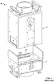
- FIG. 1 is a perspective view of a microwave-powered UV curing lamp assembly showing an irradiator and a light shield assembly in the prior art.
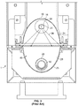
- FIG. 2 is a partial cross-sectional view of the lamp assembly of FIG. 1 showing a half-elliptical primary reflector and a light source of circular cross-section.
- FIG. 3 is a partial cross-sectional internal view of the light shield assembly of FIG. 1 showing a half-elliptical primary reflector and a light source of circular cross-section mated to a secondary reflector and end reflectors.
- the apparatus 10 includes an irradiator 12 and a light shield assembly 14.
- the irradiator 12 includes a primary reflector 16 having a generally smooth half-elliptical shape with openings 18 for receiving microwave radiation to excite a light source 20 (to be discussed herein below), and a plurality of openings 22 for receiving air flow to cool the light source 20.
- the light source 20 includes a lamp (e.g., a modular lamp, such as a microwave-powered lamp having a microwave-powered bulb (e.g., tubular bulb with a generally circular cross-section) with no electrodes or glass-to-metal seals).
- the light source 20 is placed at the internal focus of the half-ellipse formed by the primary reflector 16.
- the light source 20 and the primary reflector 16 extend linearly along an axis in a direction moving out of the page (not shown).
- a pair of end reflectors 24 (one shown) terminate opposing sides of the primary reflector 16 to form a substantially half-elliptical reflective cylinder.
- the light shield assembly 14 of FIGS. 1-3 includes a secondary reflector 25 having a substantially smooth elliptical shape.
- a second pair of end reflectors 26 terminates opposing sides of the secondary reflector 25 to form a substantially half-elliptical reflective cylinder.
- a work piece tube 30 of circular cross-section is received in circular openings 28 in the end reflectors 26.
- the center of the openings 28 and the axis of the work piece tube 30 are typically located at the external focus of the half-ellipse formed by the primary reflector 16 (i.e., the foci of the half-ellipse formed by the secondary reflector 25).
- the work piece tube 28 and the secondary reflector 25 extend linearly along an axis in a direction moving out of the page (not shown).
- gas in the light source 20 is excited to a plasma state by a source of radio frequency (RF) radiation, such as a magnetron 29 located in the irradiator 12.
- RF radio frequency
- the atoms of the excited gas in the light source 20 return to a lower energy state, thereby emitting ultraviolet light (UV).
- UV ultraviolet light
- Ultraviolet light rays 38 radiate from the light source 20 in all directions, striking the inner surfaces of the primary reflector 16, the secondary reflector 25, and the end reflectors 24, 26. Most of the ultraviolet light rays 38 are reflected toward the central axis of the work piece tube 30.
- the light source 20 and reflector design are optimized to produce the maximum peak light intensity (lamp irradiance) at a surface of a work product (also propagating linearly out of the page) placed inside the work piece tube 30.
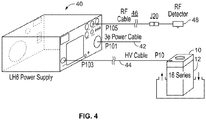
- FIG. 4 shows a plurality of cable connections between the irradiator 12 of FIGS. 1-3 and a conventional external power supply 40.
- Current irradiators manufactured by Fusion UV Systems of Gaithersburg, Maryland are powered with high voltage DC and monitored for analog parameters, such as the detection and measurement of radio-frequency (RF) and ultraviolet (UV) radiation leakage.
- the external power supply 40 includes a three-phase power cable 42 for receiving conventional AC power.
- the external power supply 40 converts AC power to high voltage DC power in the range of 4 kV-7 kV DC.
- the high voltage DC power is applied to a high voltage HV cable 44 that extends between the external power supply 40 and the irradiator 12.
- the HV cable 44 typically includes seven analog signal wires (not shown): two wires for carrying the High Voltage (HV) DC power to the irradiator 12; two wires for powering a filament associated with a microwave-powered UV-emitting bulb 20 (i.e., the light source 20); one wire each for a photo detector and a pressure switch sensor; and a seventh wire for a cable interlock.
- An RF cable 46 for monitoring microwave leakage conditions is located between the external power supply 40 and an RF detector 48, which needs to be mounted close to the irradiator 12.
- the currently employed cables 44, 46 between the external power supply 40 and the irradiator 12 have a number of drawbacks.
- the cables 44, 46 have a limited range due to losses in the cable.
- Current irradiators 12 are not user friendly for product upgrading, standardizing and compatibility. For example, certain critical monitorable paramater, including UV power, temperature, air pressure, and part type require the installation of additional sensors inside the irradiator 12.
- the cables 44, 46 do not permit changes necessary to accommodate remote monitoring of the above-cited parameter because of limited I/O and significant tethering that requires close proximity of the external power supply 40 to the irradiator 12.
- UV-emitting bulb 20 Current irradiators 12 do not permit the monitoring of UV output power that emanates from the UV-emitting bulb 20.
- Each UV-emitting bulb 20 is not identical in its UV output power.
- UV curing applications where multiple UV-emitting bulbs 20 are mounted adjacent to one another. Manual adjustments are required to lower or increase the voltage to equalize variations in UV output power from lamp to lamp. Therefore, it would be desirable to permit automatic monitoring and adjustment of UV output power.
- a monitorable pressure sensor can be integrated with a "smart blower" to automatically manage airflow and changing of speed of the "smart blower” based on data received from the monitorable pressure sensor.
- UV curing irradiator for monitoring internal sensors for performance parameters, part lifetime, and inventory control without necessitating major changes to a high voltage power supply.
- an ultraviolet curing apparatus of the kind comprising: an irradiator comprising a plurality of components; a microprocessor mounted within the irradiator; a plurality of markers in signal communication with the microprocessor and configured to monitor the plurality of components; and a plurality of sensors in signal communication with the microprocessor and configured to sense a plurality of operating conditions associated with the plurality of components.
- the above-described problems are addressed and a technical solution is achieved in the art by providing an "intelligent" irradiator that permits automated monitoring of performance parameters, part lifetime, and inventory control of internal parts.
- the irradiator includes an on lamp microprocessor.
- the on lamp microprocessor may be configured to recognize internal parts, record accumulated working time for each part, sample and process data from the plurality of sensors, and communicate with a master computer processor located within an external "intelligent" power supply via a serial bus cable.
- the on lamp microprocessor is configured to communicate with a plurality of intelligent markers (IMs) associated with one or more internal magnetrons and an internal primary reflector.
- the intelligent markers may comprise at least one of a radio frequency identification tag (RFID) or a small footprint microcontroller adhered to each part to be monitored.
- RFID radio frequency identification tag
- the on lamp microprocessor communicates with the IMs via standard serial links such as a serial peripheral interface (SPI) bus.
- SPI serial peripheral interface
- the on lamp microprocessor also communicates with a plurality of analog/digital sensors that includes one or more temperature detectors operating as a bulb recognizer (BR), an air pressure sensor for detecting a rate of air flow from an internal fan within the irradiator, a UV power sensor, and an RF detector for microwave leaking detection.
- BR bulb recognizer
- an air pressure sensor for detecting a rate of air flow from an internal fan within the irradiator
- UV power sensor a UV power sensor
- RF detector for microwave
- the "intelligent" irradiator communicates with an “intelligent” external power supply modified to include a master computer processor for controlling the irradiator and reading data processes by the on lamp microprocessor over a digital serial communication bus for communication between the irradiator and the power supply using an inexpensive standard communication protocol (e.g., CAN bus).
- a master computer processor for controlling the irradiator and reading data processes by the on lamp microprocessor over a digital serial communication bus for communication between the irradiator and the power supply using an inexpensive standard communication protocol (e.g., CAN bus).
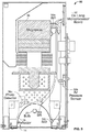
- FIG. 5 is a partial cross-sectional view of the UV curing irradiator 12 of FIG. 2 modified to include intelligent control (i.e., an irradiator 50), according to an embodiment of the present invention.
- the irradiator 50 includes an on-lamp microprocessor board 52, a plurality of intelligent markers 54a-54n (labeled IM1-IMn), and a plurality of sensors 56a-56n (e.g., a bulb recognizer labeled BR 56a, an air pressure sensor 56b, and a photo detector 56c), configured as shown.
- the placement of the components 52, 54a-54n, and 56a-56n in FIG. 5 represents a preferred, though not exclusive layout.
- a description of each of the intelligent components 52, 54a-54n, and 56a-56n is presented in connection with FIG. 6 hereinbelow.
- FIG. 6 depicts a plurality of cable connections between the irradiator 50 and an external power supply 60 modified to operate with the irradiator 50, according to an embodiment of the present invention.
- the external power supply 60 includes a three-phase power cable 42 for receiving conventional AC power.
- the external power supply 60 converts AC power to high voltage DC power in the range of 4 kV-7 kV DC.
- the high voltage DC power is applied to a modified high voltage (HV) cable 62 extending between the external power supply 60 and the irradiator 50.
- the HV cable 62 includes two wires for carrying the High Voltage (HV) DC power and a plurality of additional conductors for controlling and monitoring of the filiment current of the magnetron 29.
- a serial bus cable 63 includes two or more digital serial communication wires for communication between the external power supply 60 and the irradiator 50 using a standard serial communication protocol (e.g., a CAN bus).
- a master computer processor 64 within the external power supply 60 is configured to control and receive serial data to/from the on-lamp microprocessor board 52.
- the master computer processor 64 is also configured to communicate with an external intelligent control system (not shown) for receiving commands from and presenting data to a user 66 on a monitor 68 over a standard serial link 70 (e.g., CAN bus).
- An RF cable 72 for monitoring microwave radiation leakage from the irradiator 50 extends from the external power supply 60 to an RF detector 76. Note that the RF cable 72 associated with the RF detector 76 is generally a short local cable compared to a relatively long cable connected between the irradiator 12 and the external power supply 40 of FIG. 2 .
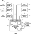
- FIG. 7 is an electrical schematic block diagram of the on lamp microprocessor board 52 mounted within the irradiator 50 of FIGS. 5 and 6 , according to an embodiment of the present invention.
- the on lamp microprocessor board 52 includes an on lamp microprocessor 80 in signal communication with a computer-readable storage medium 82 (i.e., volatile and non-volatile memor, such as RAM and Flash memory, respectively).
- the on lamp microprocessor 80 may be any commercial 8/16 bit microprocessor having sufficient speed to process command and data from the plurality of sensors 56a-56n via an 8 channel analog-to-digital converter (ADC) 84 via a sensor port 86.
- ADC analog-to-digital converter
- the on lamp microprocessor 80 further controls and reads digital data from the plurality of intelligent markers 54a-54n (labeled IM1-IMn) via a serial bus 88 and serial bus port 90 that employs a standard serial bus protocol that may be, but is not limited to, the Serial Peripheral Interface bus (SPI bus) protocol.
- SPI bus Serial Peripheral Interface bus
- on lamp microprocessor 80 may be configured to: (1) recognize parts, including one or two magnetrons 29 associated with the intelligent markers IM1 and IM2, respectively, the primary reflector 16 associated with the intelligent marker IM3, and, the microwave-powered, UV-emitting bulb 20 (i.e., the light source 20) associated with the bulb recognizer (BR); (2) record accumulated working time for each part, which is storable in non-volatile memory (i.e., the computer-readable storage medium 82); (3) sample and process data from the plurality of sensors 56a-56n, which may include, but are not limited to, one or more temperature sensors 56a operating as the bulb recognizer (BR) for detecting the type of the UV-emitting bulb 20, an air pressure sensor 56b for detecting the rate of air flow from an internal fan (not shown) within the irradiator 50, a photo detector 56c for measuing UV light output from the irradiator 50, and other optional sensors such as a filament current sensor and an HV cable
- Parts may be recognized by analog/digital means via the plurality of sensors 56a-56n over the sensor port 86 (e.g., the bulb recognizer (BR)) and digital means via the intelligent markers 54a-54n (labeled IM1-IMn) over the serial bus port 90.
- an intelligent marker refers to, but is not limited to, a semiconductor chip that permanently maintains manufacturing information, such as, but not limited to, a produced date, a part number, and a life time limit.
- the irradiator 50 may include, but is not limited to, one or both of two types of IMs: a radio frequency identification tag (RFID) or a small footprint microcontroller.
- RFID radio frequency identification tag
- An IM may be permanently adhered to a part using epoxy or other adhesive.
- RFID tag When an IM is an RFID tag, the RFID tag is configured to communicate wirelessly via radio frequency (RF) waves for exchanging data with a reader (not shown).
- RF radio frequency
- RFID tags have been employed in such diverse applications as driver licenses, passports, and bus, metro and, highway passes.
- Current RFID tag designs, such as the RFID tag 92 shown in FIG. 8A include a semiconductor chip 94 and a coiled antenna 96.
- the RFID tag 92 is not suitable for mounting directly on a magnetron 29 or a reflector since the magnetron 29/reflector it is made of metal.
- the metal of the magnetron 29/reflector shields the coiled antenna 96, thereby reducing the production of sufficient current for "reading" RFID data stored from the semicondor chip 94.
- An improvement is shown in FIG. 8B , wherein the magnetron 29/reflector does not shield a coiled antenna 98 of an RFID tag 100 because the coiled antenna is located in a vertical plane, while a chip 102 of the RFID tag 100 is located and mounted on the magnetron 29/reflector in a horizontal plane.
- An alternative solution for implementing an IM is to employ a microcontroller with a very small footprint, such as the 8-bit PIC10F222T-I/OT microcontroller produced by Microchip Technology or the ATTINY10-TSHR produced by Atmel.
- the small footprint microcontroller type IM may be connected to the on lamp microprocessor board 52 via 3 to 5 wires.
- the on lamp microprocessor 80 communicates with the small footprint microcontroller via the serial bus 88 over the serial bus port 90 to access information pre-written by the manufacturer of the part to be tracked.
- a major difficulty in implementing an IM for use as a recognizer (BR) is the high operating temperature of the UV-emitting bulb 20.
- a fully-operating UV-emitting bulb 20 has a temperature in the range of about 700 °C-900 °C, which may damage all but a few expensive military specification microcontrollers.
- the IM would be exposed to high levels of UV and microwave radiation. Therefore, adhering an inexpensive semiconductor-based IM to the UV-emitting bulb 20 is prohibitive.
- An alternative implementation of a BR may take advantage of a characteristic of mirowave-powered bulbs manufactured by Fusion UV Systems, Inc. of Gaithersburg, MD. Such bulbs contain a trace amount of an isotope of the radioactive element Krypton (i.e., "Kr 85"), which decays to non-radioactive byproducts after a predetermined amount of time (i.e., just enough to permit the microwave-powered bulb to reach operating temperature). If an irradiator does not employ Kr 85, the time for the microwave-powered bulb to ramp up to full operating temperature is significantly extended, resulting in potential harmful effects to the magnetron 29. In such circumstances, a sensor may be employed that recognizes the presence of Kr 85.
- a sensor that detects radiation emitted by Kr 85 may be remotely mounted at a safe distance from the UV-emitting bulb 20 within the irradiator 50.
- a radiation detector-based sensor may include, but is not limited to, a small Geiger counter, a CMOS or CCD imager that is operable with the the on lamp microprocessor 80 to recognize the emission spectrum of Kr 85, or in a perferred embodiment, a PIN diode used as a radiation detector, such as the UM9441 or UM9442 manfuactured by Microsemi Corp.
- Still another approach for implementing a BR is to analyze the behavior of the UV-emitting bulb 20 in the presence of Krypton.
- the emission spectrum from the UV-emitting bulb 20 has a characteristic optical transition wavelength specific to Krypton. This optical transition wavelength will only be emitted when the UV-emitting bulb 20 is first ignited, when mercury pressure is very low.
- a photo detector may then be employed as the BR to detect the brief Krypton emission during ignition.
- Certain internal parts of the irradiator 50 monitored by the IMs 54a-54n are intended to be disposable, such as, but not limited to, the UV-emitting bulb 20 and the primary reflector 16. All disposable parts inside the irradiator 50 may have pre-written information stored in the IMs 54a-54n as part of an inventory tracking system. Stored information may include, but is not limited to, a part number, a manufacturing date, and a life time limit. The data representing this information may be communicated from the IMs 54a-54n to the on lamp microprocessor 80 and then to to the master computer processor 64 in the external power supply 60.
- the on lamp microprocessor 80 In operation, upon initial installation and any subsequent installation of each of the disposable parts, information stored in the IMs 54a-54n may be read by the on lamp microprocessor 80 over the serial bus 88.
- the on lamp microprocessor 80 assigns to each part a part ID.
- the on lamp microprocessor 80 records a start date and time for each of the monitored parts.
- the on lamp microprocessor 80 may compare the working time of the part to its expected maximum life time.
- the on lamp microprocessor 80 sends a message over serial bus cable 63 to the master computer processor 64 within external power supply 50, and from there to the user via the serial link 70 (e.g., a CAN bus serial link) and/or a network (e.g., the Internet), that it is time to check and/or replace the part.
- An external monitoring system at the user site may be configured to count and display the working time of each part.
- the on lamp microprocessor 80 may store a life time limit for each part that is 20%-30% greater than the stated manufacturer's life time limit. When the working time exceeds the stored life time limit, the part and/or the irradiator 50 may be disabled by the master computer processor 64 or by shutting down the external power supply 60.
- the irradiator 50 is upgradable without requiring changes to the external power supply 60 or the cables 62, 63.
- the irradiator 50 may be equipped with an optional non-contact infrared (IR) sensor employed as a temperature sensor.
- IR infrared
- Employing a non-contact temperature sensor avoids damage due to potential overheating of the UV-emitting bulb 20, which may reach temperatures upwards of 1000°C.
- An exemplary IR sensor suitable for use in the irradiator 50 is a TPD 333/733 thermopile manufactued by Perkin Elmer.
- the irradiator 50 may also be equipped with an optional UV sensor for detecting the power level of UV radiation emitted by the UV-emitting bulb 20.
- a type of UV power sensor suitable for use in the irradiator 50 may include is a UV light power density photodiode.
- a measured output UV power level (not shown) is used as an aid for manual adjustment of UV light power output.
- the conventional external power supply 40 of FIG. 4 may be equipped (not shown) with a display that indicates only the percentage electric power needed for driving the magnetron 29.
- Conventional irradiators 12 are operable to employ UV-emitting bulbs 20 of different lengths and types. For a particular length and type of the UV-emitting bulb 20, it is necessary for a user to manually employ an external UV light power detector to measure the UV light power emanating from the UV-emitting bulb 20. Employing an on-lamp UV power detector permits automatic adjustment and display of UV power without any manual calibration.
- one or more of the sensors 56a-56n may be replaced with one or more photo detectors operable to perform several of the functions outlined above, including Kr 85 characteristic measurements, UV power detection, and a light interlock function.
- the irradiator 50 illustrated in FIGS. 5-8B has several advantages over the prior art irradiator 12 illustrated in FIGS. 1-3 .
- the digital serial communication wires within the serial bus cable 63 are configured primarily for carrying device configuration, command, and status transmission.
- data flow between the on lamp microprocessor 80 and the master computer processor 64 is relatively low, thereby permitting the use of an inexpensive standard communication protocol/cables (e.g., a CAN bus).
- the on lamp microprocessor 80 is responsible for processing data received from the plurality of sensors 56a-56n the IMs 54a-54n locally, with only processed results sent to the master computer processor 64.
- the IMs 54a-54n and the on lamp microprocessor board 52 are local connections within the irradiator 50, only wiring for power and serial communication within the HV cable 62 and the serial bus cable 63, respectively, are needed between the irradiator 50 and the external power supply 60.
- the HV cable 62 and the serial bus cable 63 are lower cost alternatives to the HV cable 44.
- the quality of signals is improved, and the distance between the irradiator 50 and the external power supply 60 may be varied. In some application, it may be desirable to shorten the HV cable 62 and the serial bus cable 63 to improve signal transmission quality and reduce cabling costs.
- the external power supply 60 and the irradiator 50 may be located on different floors of a facility. Still further, it is relatively easy to add additional sensors to the irradiator 50 without modifying the HV cable 62 and/or serial bus cable 63 and/or any port/board within the external power supply 60.
Landscapes
- Physics & Mathematics (AREA)
- Engineering & Computer Science (AREA)
- Plasma & Fusion (AREA)
- General Engineering & Computer Science (AREA)
- High Energy & Nuclear Physics (AREA)
- Physical Or Chemical Processes And Apparatus (AREA)
- Plasma Technology (AREA)
- Heating, Cooling, Or Curing Plastics Or The Like In General (AREA)
Description
- The invention relates generally to ultraviolet (UV) curing lamp assemblies, and more particularly, to a UV curing lamp assembly that includes on-board intelligence for automated inventory and monitoring of internal parts.
- Radiant energy is used in a variety of manufacturing processes to treat surfaces, films, and coatings applied to a wide range of materials. Specific processes include, but are not limited to, curing (i.e., fixing, polymerization), oxidation, purification, and disinfection. Processes employing radiant energy to polymerize or effect a desired chemical change are rapid and often less expensive compared to a thermal treatment. The radiation can also be localized to control surface processes and allow preferential curing only where the radiation is applied. Curing can also be localized within the coating or thin film to interfacial regions or in the bulk of the coating or thin film. Control of the curing process is achieved through selection of the radiation source type, physical properties (for example, spectral characteristics), spatial and temporal variation of the radiation, and curing chemistry (for example, coating composition).
- A variety of radiation sources are used for curing, fixing, polymerization, oxidation, purification, or disinfections applications. Examples of such sources include, but are not limited to, photon, electron, or ion beam sources. Typical photon sources include, but are not limited to, arc lamps, incandescent lamps, electrodeless lamps and a variety of electronic and solid-state sources (i.e., lasers). Conventional arc type UV lamp systems and microwave-driven UV lamp systems use tubular bulb envelopes made of fused quartz glass or fused silica.
-
FIG. 1 is a perspective view of a microwave-powered UV curing lamp assembly showing an irradiator and a light shield assembly in the prior art.FIG. 2 is a partial cross-sectional view of the lamp assembly ofFIG. 1 showing a half-elliptical primary reflector and a light source of circular cross-section.FIG. 3 is a partial cross-sectional internal view of the light shield assembly ofFIG. 1 showing a half-elliptical primary reflector and a light source of circular cross-section mated to a secondary reflector and end reflectors. - Referring now to
FIGS. 1-3 , theapparatus 10 includes anirradiator 12 and alight shield assembly 14. Theirradiator 12 includes aprimary reflector 16 having a generally smooth half-elliptical shape withopenings 18 for receiving microwave radiation to excite a light source 20 (to be discussed herein below), and a plurality ofopenings 22 for receiving air flow to cool thelight source 20. Thelight source 20 includes a lamp (e.g., a modular lamp, such as a microwave-powered lamp having a microwave-powered bulb (e.g., tubular bulb with a generally circular cross-section) with no electrodes or glass-to-metal seals). Thelight source 20 is placed at the internal focus of the half-ellipse formed by theprimary reflector 16. Thelight source 20 and theprimary reflector 16 extend linearly along an axis in a direction moving out of the page (not shown). A pair of end reflectors 24 (one shown) terminate opposing sides of theprimary reflector 16 to form a substantially half-elliptical reflective cylinder. Thelight shield assembly 14 ofFIGS. 1-3 includes asecondary reflector 25 having a substantially smooth elliptical shape. A second pair of end reflectors 26 (one shown) terminates opposing sides of thesecondary reflector 25 to form a substantially half-elliptical reflective cylinder. - A
work piece tube 30 of circular cross-section is received incircular openings 28 in theend reflectors 26. The center of theopenings 28 and the axis of thework piece tube 30 are typically located at the external focus of the half-ellipse formed by the primary reflector 16 (i.e., the foci of the half-ellipse formed by the secondary reflector 25). Thework piece tube 28 and thesecondary reflector 25 extend linearly along an axis in a direction moving out of the page (not shown). - In operation, gas in the
light source 20 is excited to a plasma state by a source of radio frequency (RF) radiation, such as amagnetron 29 located in theirradiator 12. The atoms of the excited gas in thelight source 20 return to a lower energy state, thereby emitting ultraviolet light (UV).Ultraviolet light rays 38 radiate from thelight source 20 in all directions, striking the inner surfaces of theprimary reflector 16, thesecondary reflector 25, and theend reflectors ultraviolet light rays 38 are reflected toward the central axis of thework piece tube 30. Thelight source 20 and reflector design are optimized to produce the maximum peak light intensity (lamp irradiance) at a surface of a work product (also propagating linearly out of the page) placed inside thework piece tube 30. -
FIG. 4 shows a plurality of cable connections between theirradiator 12 ofFIGS. 1-3 and a conventionalexternal power supply 40. Current irradiators manufactured by Fusion UV Systems of Gaithersburg, Maryland are powered with high voltage DC and monitored for analog parameters, such as the detection and measurement of radio-frequency (RF) and ultraviolet (UV) radiation leakage. Theexternal power supply 40 includes a three-phase power cable 42 for receiving conventional AC power. Theexternal power supply 40 converts AC power to high voltage DC power in the range of 4 kV-7 kV DC. The high voltage DC power is applied to a highvoltage HV cable 44 that extends between theexternal power supply 40 and theirradiator 12. TheHV cable 44 typically includes seven analog signal wires (not shown): two wires for carrying the High Voltage (HV) DC power to theirradiator 12; two wires for powering a filament associated with a microwave-powered UV-emitting bulb 20 (i.e., the light source 20); one wire each for a photo detector and a pressure switch sensor; and a seventh wire for a cable interlock. AnRF cable 46 for monitoring microwave leakage conditions is located between theexternal power supply 40 and anRF detector 48, which needs to be mounted close to theirradiator 12. - Unfortunately, the currently employed
cables external power supply 40 and theirradiator 12 have a number of drawbacks. Thecables Current irradiators 12 are not user friendly for product upgrading, standardizing and compatibility. For example, certain critical monitorable paramater, including UV power, temperature, air pressure, and part type require the installation of additional sensors inside theirradiator 12. Thecables external power supply 40 to theirradiator 12. -
Current irradiators 12 do not permit the monitoring of UV output power that emanates from the UV-emitting bulb 20. Each UV-emitting bulb 20 is not identical in its UV output power. There are certain UV curing applications where multiple UV-emittingbulbs 20 are mounted adjacent to one another. Manual adjustments are required to lower or increase the voltage to equalize variations in UV output power from lamp to lamp. Therefore, it would be desirable to permit automatic monitoring and adjustment of UV output power. - Currently employed pressure switches (not shown) do not permit real time monitoring of air pressure inside the
irradiator 12. The rate of flow of air inside theirradiator 12 is critical to the life of the UV-emittingbulb 20 and themagnetron 29. It is therefore desirable to install a monitorable pressure sensor that can transmit real time data back to a controller. Further, a monitorable pressure sensor can be integrated with a "smart blower" to automatically manage airflow and changing of speed of the "smart blower" based on data received from the monitorable pressure sensor. - Accordingly, what would be desirable, but has not yet been provided, is a microprocessor-controlled UV curing irradiator for monitoring internal sensors for performance parameters, part lifetime, and inventory control without necessitating major changes to a high voltage power supply.
- By way of further and particular background reference is made to the following publications:
- European Patent Application Publication No.
EP 2 508 255 A1 ; - United States Patent Application Publication No.
US 2001/005172 A1 to Miyashita et al. ; - International Patent Application Publication No.
WO 2009/084016 A2 ; - International Patent Application Publication No.
WO 01/45471 A1 - United States Patent No.
US 6 847 170 B2 to Kayser ; and - International Patent Application Publication No.
WO 2009/035454 A1 . - Each of the above-mentioned references discloses an ultraviolet curing apparatus of the kind comprising: an irradiator comprising a plurality of components; a microprocessor mounted within the irradiator; a plurality of markers in signal communication with the microprocessor and configured to monitor the plurality of components; and a plurality of sensors in signal communication with the microprocessor and configured to sense a plurality of operating conditions associated with the plurality of components.
- The present invention is defined in the appended independent claim,
claim 1 to which reference should be made. Advantageous features are set out in the appended dependent claims. - The above-described problems are addressed and a technical solution is achieved in the art by providing an "intelligent" irradiator that permits automated monitoring of performance parameters, part lifetime, and inventory control of internal parts. The irradiator includes an on lamp microprocessor. The on lamp microprocessor may be configured to recognize internal parts, record accumulated working time for each part, sample and process data from the plurality of sensors, and communicate with a master computer processor located within an external "intelligent" power supply via a serial bus cable.
- According to an embodiment of the present invention, the on lamp microprocessor is configured to communicate with a plurality of intelligent markers (IMs) associated with one or more internal magnetrons and an internal primary reflector. The intelligent markers may comprise at least one of a radio frequency identification tag (RFID) or a small footprint microcontroller adhered to each part to be monitored. The on lamp microprocessor communicates with the IMs via standard serial links such as a serial peripheral interface (SPI) bus. The on lamp microprocessor also communicates with a plurality of analog/digital sensors that includes one or more temperature detectors operating as a bulb recognizer (BR), an air pressure sensor for detecting a rate of air flow from an internal fan within the irradiator, a UV power sensor, and an RF detector for microwave leaking detection.
- The "intelligent" irradiator communicates with an "intelligent" external power supply modified to include a master computer processor for controlling the irradiator and reading
data processes by the on lamp microprocessor over a digital serial communication bus for communication between the irradiator and the power supply using an inexpensive standard communication protocol (e.g., CAN bus). - The present invention may be more readily understood from the detailed description of an exemplary embodiment presented below considered in conjunction with the attached drawings and in which like reference numerals refer to similar elements and in which:
-
FIG. 1 is a perspective view of a UV curing lamp assembly showing an irradiator and a light shield assembly in the prior art; -
FIG. 2 is a partial cross-sectional view of the lamp assembly ofFIG. 1 showing a half-elliptical primary reflector and a light source of circular cross-section; -
FIG. 3 is a partial cross-sectional internal view of the lamp assembly interconnected with the light shield assembly ofFIG. 1 , showing a half-elliptical primary reflector and a light source of circular cross-section mated to a secondary reflector and end reflectors; -
FIG. 4 shows a plurality of cable connections between the irradiator ofFIGS. 1-3 and a conventional external power supply; -
FIG. 5 is a partial cross-sectional view of the irradiator ofFIG. 2 modified to include intelligent control, according to an embodiment of the present invention; -
FIG. 6 shows a plurality of cable connections between the irradiator ofFIG. 5 and an external power supply modified to operate with the irradiator, according to an embodiment of the present invention; -
FIG. 7 is an electrical schematic block diagram of the on lamp microprocessor board mounted within the irradiator ofFIGS. 5 and6 , according to an embodiment of the present invention; -
FIG. 8A depicts a conventional RFID tag having a semiconductor chip and a coiled antenna located within a common plane; and -
FIG. 8B depicts a modified version of the RFID tag ofFIG. 8A , wherein a semiconductor chip is located in the horizontal plane and the coiled antenna is located in the vertical plane, according to an embodiment of the present invetion. - It is to be understood that the attached drawings are for purposes of illustrating the concepts of the invention and may not be to scale.
-
FIG. 5 is a partial cross-sectional view of theUV curing irradiator 12 ofFIG. 2 modified to include intelligent control (i.e., an irradiator 50), according to an embodiment of the present invention. Theirradiator 50 includes an on-lamp microprocessor board 52, a plurality ofintelligent markers 54a-54n (labeled IM1-IMn), and a plurality ofsensors 56a-56n (e.g., a bulb recognizer labeledBR 56a, anair pressure sensor 56b, and aphoto detector 56c), configured as shown. The placement of thecomponents FIG. 5 represents a preferred, though not exclusive layout. A description of each of theintelligent components FIG. 6 hereinbelow. -
FIG. 6 depicts a plurality of cable connections between the irradiator 50 and anexternal power supply 60 modified to operate with theirradiator 50, according to an embodiment of the present invention. Theexternal power supply 60 includes a three-phase power cable 42 for receiving conventional AC power. Theexternal power supply 60 converts AC power to high voltage DC power in the range of 4 kV-7 kV DC. The high voltage DC power is applied to a modified high voltage (HV)cable 62 extending between theexternal power supply 60 and theirradiator 50. TheHV cable 62 includes two wires for carrying the High Voltage (HV) DC power and a plurality of additional conductors for controlling and monitoring of the filiment current of themagnetron 29. Aserial bus cable 63 includes two or more digital serial communication wires for communication between theexternal power supply 60 and theirradiator 50 using a standard serial communication protocol (e.g., a CAN bus). Amaster computer processor 64 within theexternal power supply 60 is configured to control and receive serial data to/from the on-lamp microprocessor board 52. Themaster computer processor 64 is also configured to communicate with an external intelligent control system (not shown) for receiving commands from and presenting data to auser 66 on amonitor 68 over a standard serial link 70 (e.g., CAN bus). AnRF cable 72 for monitoring microwave radiation leakage from theirradiator 50 extends from theexternal power supply 60 to anRF detector 76. Note that theRF cable 72 associated with theRF detector 76 is generally a short local cable compared to a relatively long cable connected between the irradiator 12 and theexternal power supply 40 ofFIG. 2 . -
FIG. 7 is an electrical schematic block diagram of the onlamp microprocessor board 52 mounted within theirradiator 50 ofFIGS. 5 and6 , according to an embodiment of the present invention. The onlamp microprocessor board 52 includes an onlamp microprocessor 80 in signal communication with a computer-readable storage medium 82 (i.e., volatile and non-volatile memor, such as RAM and Flash memory, respectively). The onlamp microprocessor 80 may be any commercial 8/16 bit microprocessor having sufficient speed to process command and data from the plurality ofsensors 56a-56n via an 8 channel analog-to-digital converter (ADC) 84 via asensor port 86. The onlamp microprocessor 80 further controls and reads digital data from the plurality ofintelligent markers 54a-54n (labeled IM1-IMn) via aserial bus 88 andserial bus port 90 that employs a standard serial bus protocol that may be, but is not limited to, the Serial Peripheral Interface bus (SPI bus) protocol. - According to an embodiment of the present invention, on
lamp microprocessor 80 may be configured to: (1) recognize parts, including one or twomagnetrons 29 associated with the intelligent markers IM1 and IM2, respectively, theprimary reflector 16 associated with the intelligent marker IM3, and, the microwave-powered, UV-emitting bulb 20 (i.e., the light source 20) associated with the bulb recognizer (BR); (2) record accumulated working time for each part, which is storable in non-volatile memory (i.e., the computer-readable storage medium 82); (3) sample and process data from the plurality ofsensors 56a-56n, which may include, but are not limited to, one ormore temperature sensors 56a operating as the bulb recognizer (BR) for detecting the type of the UV-emittingbulb 20, anair pressure sensor 56b for detecting the rate of air flow from an internal fan (not shown) within theirradiator 50, aphoto detector 56c for measuing UV light output from theirradiator 50, and other optional sensors such as a filament current sensor and an HV cable interlock (not shown); and (4) communicate with themaster computer processor 64 withinexternal power supply 60 via theserial bus cable 63. - Parts may be recognized by analog/digital means via the plurality of
sensors 56a-56n over the sensor port 86 (e.g., the bulb recognizer (BR)) and digital means via theintelligent markers 54a-54n (labeled IM1-IMn) over theserial bus port 90. As used herein, an intelligent marker (IM) refers to, but is not limited to, a semiconductor chip that permanently maintains manufacturing information, such as, but not limited to, a produced date, a part number, and a life time limit. Theirradiator 50 may include, but is not limited to, one or both of two types of IMs: a radio frequency identification tag (RFID) or a small footprint microcontroller. An IM may be permanently adhered to a part using epoxy or other adhesive. - When an IM is an RFID tag, the RFID tag is configured to communicate wirelessly via radio frequency (RF) waves for exchanging data with a reader (not shown). Several types of RFID products are known, such as the Texas Instruments' RI-103-114A-01 and ATMEL's AT88SCRF-ADK2. RFID tags have been employed in such diverse applications as driver licenses, passports, and bus, metro and, highway passes. Current RFID tag designs, such as the
RFID tag 92 shown inFIG. 8A , include asemiconductor chip 94 and acoiled antenna 96. TheRFID tag 92 is not suitable for mounting directly on amagnetron 29 or a reflector since themagnetron 29/reflector it is made of metal. The metal of themagnetron 29/reflector shields the coiledantenna 96, thereby reducing the production of sufficient current for "reading" RFID data stored from thesemicondor chip 94. An improvement is shown inFIG. 8B , wherein themagnetron 29/reflector does not shield a coiledantenna 98 of anRFID tag 100 because the coiled antenna is located in a vertical plane, while achip 102 of theRFID tag 100 is located and mounted on themagnetron 29/reflector in a horizontal plane. - An alternative solution for implementing an IM is to employ a microcontroller with a very small footprint, such as the 8-bit PIC10F222T-I/OT microcontroller produced by Microchip Technology or the ATTINY10-TSHR produced by Atmel. The small footprint microcontroller type IM may be connected to the on
lamp microprocessor board 52 via 3 to 5 wires. In such circumstances, the onlamp microprocessor 80 communicates with the small footprint microcontroller via theserial bus 88 over theserial bus port 90 to access information pre-written by the manufacturer of the part to be tracked. - A major difficulty in implementing an IM for use as a recognizer (BR) is the high operating temperature of the UV-emitting
bulb 20. A fully-operating UV-emittingbulb 20 has a temperature in the range of about 700 °C-900 °C, which may damage all but a few expensive military specification microcontrollers. In addition, the IM would be exposed to high levels of UV and microwave radiation. Therefore, adhering an inexpensive semiconductor-based IM to the UV-emittingbulb 20 is prohibitive. - An alternative implementation of a BR may take advantage of a characteristic of mirowave-powered bulbs manufactured by Fusion UV Systems, Inc. of Gaithersburg, MD. Such bulbs contain a trace amount of an isotope of the radioactive element Krypton (i.e., "Kr 85"), which decays to non-radioactive byproducts after a predetermined amount of time (i.e., just enough to permit the microwave-powered bulb to reach operating temperature). If an irradiator does not employ Kr 85, the time for the microwave-powered bulb to ramp up to full operating temperature is significantly extended, resulting in potential harmful effects to the
magnetron 29. In such circumstances, a sensor may be employed that recognizes the presence of Kr 85. A sensor that detects radiation emitted by Kr 85 may be remotely mounted at a safe distance from the UV-emittingbulb 20 within theirradiator 50. A radiation detector-based sensor may include, but is not limited to, a small Geiger counter, a CMOS or CCD imager that is operable with the the onlamp microprocessor 80 to recognize the emission spectrum of Kr 85, or in a perferred embodiment, a PIN diode used as a radiation detector, such as the UM9441 or UM9442 manfuactured by Microsemi Corp. - Still another approach for implementing a BR is to analyze the behavior of the UV-emitting
bulb 20 in the presence of Krypton. During bulb ignition, the emission spectrum from the UV-emittingbulb 20 has a characteristic optical transition wavelength specific to Krypton. This optical transition wavelength will only be emitted when the UV-emittingbulb 20 is first ignited, when mercury pressure is very low. A photo detector may then be employed as the BR to detect the brief Krypton emission during ignition. - Certain internal parts of the
irradiator 50 monitored by theIMs 54a-54n are intended to be disposable, such as, but not limited to, the UV-emittingbulb 20 and theprimary reflector 16. All disposable parts inside theirradiator 50 may have pre-written information stored in theIMs 54a-54n as part of an inventory tracking system. Stored information may include, but is not limited to, a part number, a manufacturing date, and a life time limit. The data representing this information may be communicated from theIMs 54a-54n to the onlamp microprocessor 80 and then to to themaster computer processor 64 in theexternal power supply 60. - In operation, upon initial installation and any subsequent installation of each of the disposable parts, information stored in the
IMs 54a-54n may be read by the onlamp microprocessor 80 over theserial bus 88. The onlamp microprocessor 80 assigns to each part a part ID. The onlamp microprocessor 80 records a start date and time for each of the monitored parts. The onlamp microprocessor 80 may compare the working time of the part to its expected maximum life time. When the working time approaches or exceeds a preestablished expiration date, the onlamp microprocessor 80 sends a message overserial bus cable 63 to themaster computer processor 64 withinexternal power supply 50, and from there to the user via the serial link 70 (e.g., a CAN bus serial link) and/or a network (e.g., the Internet), that it is time to check and/or replace the part. An external monitoring system at the user site may be configured to count and display the working time of each part. Aditionally, the onlamp microprocessor 80 may store a life time limit for each part that is 20%-30% greater than the stated manufacturer's life time limit. When the working time exceeds the stored life time limit, the part and/or theirradiator 50 may be disabled by themaster computer processor 64 or by shutting down theexternal power supply 60. - The
irradiator 50 is upgradable without requiring changes to theexternal power supply 60 or thecables irradiator 50 may be equipped with an optional non-contact infrared (IR) sensor employed as a temperature sensor. Employing a non-contact temperature sensor avoids damage due to potential overheating of the UV-emittingbulb 20, which may reach temperatures upwards of 1000°C. An exemplary IR sensor suitable for use in theirradiator 50 is a TPD 333/733 thermopile manufactued by Perkin Elmer. - The
irradiator 50 may also be equipped with an optional UV sensor for detecting the power level of UV radiation emitted by the UV-emittingbulb 20. A type of UV power sensor suitable for use in theirradiator 50 may include is a UV light power density photodiode. In theprior art irradiator 12, a measured output UV power level (not shown) is used as an aid for manual adjustment of UV light power output. The conventionalexternal power supply 40 ofFIG. 4 may be equipped (not shown) with a display that indicates only the percentage electric power needed for driving themagnetron 29. -
Conventional irradiators 12 are operable to employ UV-emittingbulbs 20 of different lengths and types. For a particular length and type of the UV-emittingbulb 20, it is necessary for a user to manually employ an external UV light power detector to measure the UV light power emanating from the UV-emittingbulb 20. Employing an on-lamp UV power detector permits automatic adjustment and display of UV power without any manual calibration. - According to an embodiment of the present invention, referring gain to
FIG. 6 , one or more of thesensors 56a-56n may be replaced with one or more photo detectors operable to perform several of the functions outlined above, including Kr 85 characteristic measurements, UV power detection, and a light interlock function. - The
irradiator 50 illustrated inFIGS. 5-8B has several advantages over theprior art irradiator 12 illustrated inFIGS. 1-3 . The digital serial communication wires within theserial bus cable 63 are configured primarily for carrying device configuration, command, and status transmission. As a result, data flow between the onlamp microprocessor 80 and themaster computer processor 64 is relatively low, thereby permitting the use of an inexpensive standard communication protocol/cables (e.g., a CAN bus). According to an embodiment of the present invention, the onlamp microprocessor 80 is responsible for processing data received from the plurality ofsensors 56a-56n theIMs 54a-54n locally, with only processed results sent to themaster computer processor 64. - Referring again to
FIG. 6 , since all of connections between thesensors 56a-56n, theIMs 54a-54n and the onlamp microprocessor board 52 are local connections within theirradiator 50, only wiring for power and serial communication within theHV cable 62 and theserial bus cable 63, respectively, are needed between the irradiator 50 and theexternal power supply 60. As a result, theHV cable 62 and theserial bus cable 63 are lower cost alternatives to theHV cable 44. Further, the quality of signals is improved, and the distance between the irradiator 50 and theexternal power supply 60 may be varied. In some application, it may be desirable to shorten theHV cable 62 and theserial bus cable 63 to improve signal transmission quality and reduce cabling costs. Alternatively, it may be desirable to increase the length of theHV cable 62 and theserial bus cable 63 so that theexternal power supply 60 and theirradiator 50 may be located on different floors of a facility. Still further, it is relatively easy to add additional sensors to theirradiator 50 without modifying theHV cable 62 and/orserial bus cable 63 and/or any port/board within theexternal power supply 60. - It is to be understood that the exemplary embodiments are merely illustrative of the invention and that many variations of the above-described embodiments may be devised by one skilled in the art. The scope of the invention is defined by the following claims.
Claims (13)
- A microwave-powered ultraviolet curing lamp apparatus, comprising:an irradiator (12; 50) comprising an ultraviolet 'UV' curing lamp (20), and a plurality of components including one or more magnetrons (29) to excite the UV curing lamp and a primary reflector (16);a microprocessor (80) mounted within the irradiator (12; 50);a plurality of markers (54a-54n) in signal communication with the microprocessor (80) and configured to monitor at least one of the one or more magnetrons and the primary radiator among the plurality of components, wherein the plurality of markers (54a-54n) comprises at least one of a radio frequency identification tag (92; 100) and a small footprint microcontroller (-); anda plurality of sensors (56a-56n) in signal communication with the microprocessor (80) and configured to sense a plurality of operating conditions associated with the plurality of components.
- The apparatus of claim 1, wherein a respective small footprint microcontroller is configured to be adhered to each monitored component (52).
- The apparatus of claim 1, wherein the microprocessor (80) is configured to communicate with each of the plurality of markers (54a-54n) through a standard serial bus (63; 88).
- The apparatus of claim 3, wherein the standard serial bus (63; 88) is the serial peripheral interface bus.
- The apparatus of claim 1 wherein each of the plurality of markers (54a-54n) is configured to maintain manufacturing information including at least a produced date, a part number, and a lifetime limit.
- The apparatus of claim 1, wherein the microprocessor (80) is configured to:recognize type and parameters of each of the plurality of components (52);record accumulated working time of each of the plurality of components (52);sample and process data from the plurality of sensors (56a-56n); andcommunicate with a master computer processor (64) via a serial bus (63).
- The apparatus of claim 6, wherein the serial bus (63; 88) is a controller area network 'CAN' bus.
- The apparatus of claim 1, wherein the plurality of sensors (56a-56n) is at least one of one or more temperature detectors operating as a bulb recognizer (56a), an air pressure sensor (56b) for detecting a rate of air flow from an internal fan, an ultra-violet 'UV' power sensor (56c), and a radio frequency 'RF' detector (76) for microwave leaking detection.
- The apparatus of claim 1, wherein the at least one radio frequency identification tag (92) comprises a coiled antenna (96) mounted in a vertical plane relative to a magnetron (29) and an internal chip mounted in a horizontal plane relative to the magnetron (29).
- The apparatus of claim 1, wherein the plurality of sensors (56a-56n) includes at least a bulb recognizer (56a) configured to recognize a presence of Kr 85 in a microwave-powered lamp within the irradiator (12; 50).
- The apparatus of claim 10, wherein the bulb recognizer (56a) is one of a Geiger counter, a CMOS or CCD imager operable with the microprocessor to recognize the emission spectrum of Kr 85, or a PIN diode.
- The apparatus of claim 10, wherein the bulb recognizer (56a) is a photo detector configured to detect an initial ignition wavelength of Kr 85.
- The apparatus of claim 10, wherein at least one of the plurality of components (52) is disposable.
Applications Claiming Priority (2)
| Application Number | Priority Date | Filing Date | Title |
|---|---|---|---|
| US13/680,882 US8785868B2 (en) | 2012-11-19 | 2012-11-19 | Intelligent UV radiation system |
| PCT/US2013/070782 WO2014078852A1 (en) | 2012-11-19 | 2013-11-19 | Intelligent uv radiation system |
Publications (3)
| Publication Number | Publication Date |
|---|---|
| EP2920792A1 EP2920792A1 (en) | 2015-09-23 |
| EP2920792A4 EP2920792A4 (en) | 2016-10-05 |
| EP2920792B1 true EP2920792B1 (en) | 2018-09-26 |
Family
ID=50727038
Family Applications (1)
| Application Number | Title | Priority Date | Filing Date |
|---|---|---|---|
| EP13855991.9A Active EP2920792B1 (en) | 2012-11-19 | 2013-11-19 | Intelligent uv radiation system |
Country Status (6)
| Country | Link |
|---|---|
| US (1) | US8785868B2 (en) |
| EP (1) | EP2920792B1 (en) |
| JP (1) | JP6324400B2 (en) |
| KR (1) | KR102193047B1 (en) |
| CN (2) | CN104956447A (en) |
| WO (1) | WO2014078852A1 (en) |
Families Citing this family (12)
| Publication number | Priority date | Publication date | Assignee | Title |
|---|---|---|---|---|
| KR102482671B1 (en) * | 2014-07-07 | 2022-12-29 | 노드슨 코포레이션 | Systems and methods for determining the suitability of rf sources in ultraviolet systems |
| JP2017533058A (en) | 2014-09-17 | 2017-11-09 | ギャリソン デンタル ソリューションズ,リミティド ライアビリティ カンパニー | Dental curing light |
| GB201500494D0 (en) | 2015-01-13 | 2015-02-25 | Gew Ec Ltd | Print curing apparatus |
| US9978580B2 (en) | 2015-11-30 | 2018-05-22 | Heraeus Noblelight America Llc | Lamps and light sources including RFID tags, and methods of assembling and operating the same |
| CN105682316A (en) * | 2016-01-06 | 2016-06-15 | 瑞昌市佳佳机电设备有限公司 | UV lamp, UV lamp starting device and UV lamp power control device |
| USD810293S1 (en) | 2017-01-20 | 2018-02-13 | Garrison Dental Solutions, Llc | Dental instrument |
| KR102430452B1 (en) | 2017-11-03 | 2022-08-05 | 헤라우스 노블라이트 아메리카 엘엘씨 | Ultraviolet lamp system and method of operation and construction thereof |
| CA3125075A1 (en) | 2019-01-18 | 2020-07-23 | Trojan Technologies Group Ulc | Lamp sensor modulation of a power supply |
| GB2588425B (en) * | 2019-10-23 | 2021-10-27 | Elekta ltd | Magnetron condition monitoring |
| CN111025025B (en) * | 2019-11-21 | 2023-03-21 | 广东美的厨房电器制造有限公司 | Method for reminding replacement of electric appliance parts |
| CN113438860A (en) * | 2021-06-08 | 2021-09-24 | 武汉中仪物联技术股份有限公司 | UV ultraviolet curing prosthetic devices's cooling system |
| KR102884171B1 (en) * | 2023-03-08 | 2025-11-14 | 주식회사 휴비츠 | UV curing machine including a hemispherical reflector |
Family Cites Families (27)
| Publication number | Priority date | Publication date | Assignee | Title |
|---|---|---|---|---|
| US4249603A (en) * | 1978-12-26 | 1981-02-10 | Occidental Oil Shale, Inc. | Doping a retort with radioactive nuclides to determine the locus of a processing zone |
| JPS63260028A (en) * | 1986-11-19 | 1988-10-27 | Tokyo Ohka Kogyo Co Ltd | Heat stabilizer for photoresist |
| CH690486A5 (en) * | 1995-07-11 | 2000-09-15 | Bob Hammer Systems Solutions S | Device for the management of fluorescent lamps. |
| CN2225252Y (en) * | 1995-08-29 | 1996-04-24 | 上海希格玛高技术公司 | Ultra-violet irradiator for treating blood platelet |
| EP1395092B1 (en) * | 1996-04-10 | 2006-05-31 | Seiko Epson Corporation | Light-source lamp unit, light-source device and projection-type display apparatus |
| US6333602B1 (en) * | 1999-12-14 | 2001-12-25 | Exfo Photonic Solutions Inc. | Smart light source with integrated operational parameters data storage capability |
| GB2360084B (en) * | 2000-03-08 | 2004-04-21 | Nordson Corp | Lamp assembly |
| JP2002143826A (en) * | 2000-08-30 | 2002-05-21 | Denso Corp | Waste recycling system and illegal dumping detection system |
| CN1350273A (en) * | 2000-10-20 | 2002-05-22 | 华能科技股份有限公司 | Radio frequency identification tag device and assembly method thereof |
| JP2003330112A (en) * | 2002-05-16 | 2003-11-19 | Nec Viewtechnology Ltd | Projector and lamp information management method used therein |
| US6940408B2 (en) * | 2002-12-31 | 2005-09-06 | Avery Dennison Corporation | RFID device and method of forming |
| US6933683B2 (en) * | 2003-02-27 | 2005-08-23 | Nordson Corporation | Microwave powered lamphead having external shutter |
| DE10333932A1 (en) * | 2003-07-25 | 2005-02-24 | Robert Bosch Gmbh | Synchronization of data processing units |
| US7042346B2 (en) * | 2003-08-12 | 2006-05-09 | Gaige Bradley Paulsen | Radio frequency identification parts verification system and method for using same |
| US7372039B2 (en) * | 2005-12-20 | 2008-05-13 | Ecolab Inc. | Near UV absorption spectrometer and method for using the same |
| JP3876365B2 (en) * | 2006-02-18 | 2007-01-31 | 株式会社キーエンス | UV irradiation equipment |
| WO2007099479A2 (en) * | 2006-03-01 | 2007-09-07 | Koninklijke Philips Electronics N. V. | Ic circuit with test access control circuit using a jtag interface |
| US7692171B2 (en) * | 2006-03-17 | 2010-04-06 | Andrzei Kaszuba | Apparatus and method for exposing a substrate to UV radiation using asymmetric reflectors |
| WO2009032301A1 (en) * | 2007-09-05 | 2009-03-12 | Analytical Instrument Systems, Inc. | Intelligent sensor data logging system |
| US20100328083A1 (en) * | 2007-09-13 | 2010-12-30 | Oakriver Technologies Inc. | System for monitoring ultraviolet radiation levels in a curing chamber and method of monitoring |
| US20090167201A1 (en) * | 2007-11-07 | 2009-07-02 | Luxim Corporation. | Light source and methods for microscopy and endoscopy |
| WO2009084016A2 (en) | 2007-12-31 | 2009-07-09 | Makarand Hari Joshi | A device with gsm chip for measuring and recording and transferring the electrical parameters & burning hours of cfl lamp |
| US8289144B2 (en) * | 2008-11-28 | 2012-10-16 | Silicon Valley Micro C Corp. | Tire parameter monitoring system with sensor location using RFID tags |
| US20120133716A1 (en) * | 2009-06-26 | 2012-05-31 | Toshihiko Aizawa | Ultraviolet irradiation device and printing device |
| CN102695558B (en) * | 2009-12-02 | 2014-04-16 | 松下神视株式会社 | UV-irradiation apparatus |
| TWI379057B (en) * | 2009-12-11 | 2012-12-11 | Ind Tech Res Inst | An led lamp |
| US8507884B2 (en) * | 2011-01-05 | 2013-08-13 | Heraeus Noblelight Fusion Uv Inc. | Elliptical light source for ultraviolet (UV) curing lamp assemblies |
-
2012
- 2012-11-19 US US13/680,882 patent/US8785868B2/en active Active
-
2013
- 2013-11-19 KR KR1020157015725A patent/KR102193047B1/en active Active
- 2013-11-19 WO PCT/US2013/070782 patent/WO2014078852A1/en not_active Ceased
- 2013-11-19 JP JP2015543114A patent/JP6324400B2/en active Active
- 2013-11-19 CN CN201380059988.2A patent/CN104956447A/en active Pending
- 2013-11-19 CN CN201910849867.7A patent/CN110548659A/en active Pending
- 2013-11-19 EP EP13855991.9A patent/EP2920792B1/en active Active
Non-Patent Citations (1)
| Title |
|---|
| None * |
Also Published As
| Publication number | Publication date |
|---|---|
| JP2016506016A (en) | 2016-02-25 |
| WO2014078852A1 (en) | 2014-05-22 |
| JP6324400B2 (en) | 2018-05-16 |
| US8785868B2 (en) | 2014-07-22 |
| EP2920792A4 (en) | 2016-10-05 |
| EP2920792A1 (en) | 2015-09-23 |
| CN104956447A (en) | 2015-09-30 |
| KR20150091330A (en) | 2015-08-10 |
| CN110548659A (en) | 2019-12-10 |
| US20140138550A1 (en) | 2014-05-22 |
| KR102193047B1 (en) | 2020-12-18 |
Similar Documents
| Publication | Publication Date | Title |
|---|---|---|
| US8785868B2 (en) | Intelligent UV radiation system | |
| EP2517268B1 (en) | Uv led based lamp for compact uv curing lamp assemblies | |
| EP2447981B2 (en) | Low-pressure mercury vapor discharge lamp with amalgam, lamp system, water treatment system, use of a lamp system | |
| KR102543349B1 (en) | Plasma monitoring apparatus | |
| EP3516932B1 (en) | Lighting device comprising a communication element for wireless communication | |
| EP3060844B1 (en) | Apparatus for radiant energy curing of coating | |
| TW200816881A (en) | Plasma generation apparatus and workpiece processing apparatus using the same | |
| KR20060004683A (en) | Infrared Emitters and Irradiation Devices | |
| US8507884B2 (en) | Elliptical light source for ultraviolet (UV) curing lamp assemblies | |
| JP4647566B2 (en) | Plasma generating apparatus and work processing apparatus using the same | |
| US9125283B2 (en) | Light source apparatus | |
| KR101927748B1 (en) | Lighting device using glass tube through which ultraviolet rays are transmitted | |
| JP4724625B2 (en) | Plasma generating apparatus and work processing apparatus using the same | |
| EP3384736B1 (en) | Lamps and light sources including rfid tags, and methods of assembling and operating the same | |
| EP3044633B1 (en) | Large area high-uniformity uv source with many small emitters | |
| JP2010055779A (en) | Ultraviolet irradiation device | |
| JP2016128800A (en) | Tunable photo-detector device | |
| CN121532667A (en) | Diamond spin sensor system | |
| CN118287352A (en) | UV (ultraviolet) quick curing device |
Legal Events
| Date | Code | Title | Description |
|---|---|---|---|
| PUAI | Public reference made under article 153(3) epc to a published international application that has entered the european phase |
Free format text: ORIGINAL CODE: 0009012 |
|
| 17P | Request for examination filed |
Effective date: 20150511 |
|
| AK | Designated contracting states |
Kind code of ref document: A1 Designated state(s): AL AT BE BG CH CY CZ DE DK EE ES FI FR GB GR HR HU IE IS IT LI LT LU LV MC MK MT NL NO PL PT RO RS SE SI SK SM TR |
|
| AX | Request for extension of the european patent |
Extension state: BA ME |
|
| DAX | Request for extension of the european patent (deleted) | ||
| RA4 | Supplementary search report drawn up and despatched (corrected) |
Effective date: 20160902 |
|
| RIC1 | Information provided on ipc code assigned before grant |
Ipc: H05B 41/36 20060101ALI20160829BHEP Ipc: G21K 5/02 20060101AFI20160829BHEP Ipc: H05B 37/03 20060101ALI20160829BHEP Ipc: G21K 5/04 20060101ALI20160829BHEP |
|
| GRAP | Despatch of communication of intention to grant a patent |
Free format text: ORIGINAL CODE: EPIDOSNIGR1 |
|
| RIC1 | Information provided on ipc code assigned before grant |
Ipc: G21K 5/02 20060101AFI20180308BHEP Ipc: G21K 5/04 20060101ALI20180308BHEP Ipc: H05B 37/03 20060101ALI20180308BHEP Ipc: H05B 41/36 20060101ALI20180308BHEP |
|
| INTG | Intention to grant announced |
Effective date: 20180409 |
|
| GRAS | Grant fee paid |
Free format text: ORIGINAL CODE: EPIDOSNIGR3 |
|
| GRAA | (expected) grant |
Free format text: ORIGINAL CODE: 0009210 |
|
| AK | Designated contracting states |
Kind code of ref document: B1 Designated state(s): AL AT BE BG CH CY CZ DE DK EE ES FI FR GB GR HR HU IE IS IT LI LT LU LV MC MK MT NL NO PL PT RO RS SE SI SK SM TR |
|
| REG | Reference to a national code |
Ref country code: GB Ref legal event code: FG4D |
|
| REG | Reference to a national code |
Ref country code: CH Ref legal event code: EP |
|
| REG | Reference to a national code |
Ref country code: AT Ref legal event code: REF Ref document number: 1046978 Country of ref document: AT Kind code of ref document: T Effective date: 20181015 |
|
| REG | Reference to a national code |
Ref country code: IE Ref legal event code: FG4D |
|
| REG | Reference to a national code |
Ref country code: DE Ref legal event code: R096 Ref document number: 602013044301 Country of ref document: DE |
|
| REG | Reference to a national code |
Ref country code: NL Ref legal event code: FP |
|
| PG25 | Lapsed in a contracting state [announced via postgrant information from national office to epo] |
Ref country code: FI Free format text: LAPSE BECAUSE OF FAILURE TO SUBMIT A TRANSLATION OF THE DESCRIPTION OR TO PAY THE FEE WITHIN THE PRESCRIBED TIME-LIMIT Effective date: 20180926 Ref country code: NO Free format text: LAPSE BECAUSE OF FAILURE TO SUBMIT A TRANSLATION OF THE DESCRIPTION OR TO PAY THE FEE WITHIN THE PRESCRIBED TIME-LIMIT Effective date: 20181226 Ref country code: RS Free format text: LAPSE BECAUSE OF FAILURE TO SUBMIT A TRANSLATION OF THE DESCRIPTION OR TO PAY THE FEE WITHIN THE PRESCRIBED TIME-LIMIT Effective date: 20180926 Ref country code: GR Free format text: LAPSE BECAUSE OF FAILURE TO SUBMIT A TRANSLATION OF THE DESCRIPTION OR TO PAY THE FEE WITHIN THE PRESCRIBED TIME-LIMIT Effective date: 20181227 Ref country code: BG Free format text: LAPSE BECAUSE OF FAILURE TO SUBMIT A TRANSLATION OF THE DESCRIPTION OR TO PAY THE FEE WITHIN THE PRESCRIBED TIME-LIMIT Effective date: 20181226 Ref country code: SE Free format text: LAPSE BECAUSE OF FAILURE TO SUBMIT A TRANSLATION OF THE DESCRIPTION OR TO PAY THE FEE WITHIN THE PRESCRIBED TIME-LIMIT Effective date: 20180926 Ref country code: LT Free format text: LAPSE BECAUSE OF FAILURE TO SUBMIT A TRANSLATION OF THE DESCRIPTION OR TO PAY THE FEE WITHIN THE PRESCRIBED TIME-LIMIT Effective date: 20180926 |
|
| REG | Reference to a national code |
Ref country code: LT Ref legal event code: MG4D |
|
| PG25 | Lapsed in a contracting state [announced via postgrant information from national office to epo] |
Ref country code: AL Free format text: LAPSE BECAUSE OF FAILURE TO SUBMIT A TRANSLATION OF THE DESCRIPTION OR TO PAY THE FEE WITHIN THE PRESCRIBED TIME-LIMIT Effective date: 20180926 Ref country code: LV Free format text: LAPSE BECAUSE OF FAILURE TO SUBMIT A TRANSLATION OF THE DESCRIPTION OR TO PAY THE FEE WITHIN THE PRESCRIBED TIME-LIMIT Effective date: 20180926 Ref country code: HR Free format text: LAPSE BECAUSE OF FAILURE TO SUBMIT A TRANSLATION OF THE DESCRIPTION OR TO PAY THE FEE WITHIN THE PRESCRIBED TIME-LIMIT Effective date: 20180926 |
|
| REG | Reference to a national code |
Ref country code: AT Ref legal event code: MK05 Ref document number: 1046978 Country of ref document: AT Kind code of ref document: T Effective date: 20180926 |
|
| PG25 | Lapsed in a contracting state [announced via postgrant information from national office to epo] |
Ref country code: IS Free format text: LAPSE BECAUSE OF FAILURE TO SUBMIT A TRANSLATION OF THE DESCRIPTION OR TO PAY THE FEE WITHIN THE PRESCRIBED TIME-LIMIT Effective date: 20190126 Ref country code: ES Free format text: LAPSE BECAUSE OF FAILURE TO SUBMIT A TRANSLATION OF THE DESCRIPTION OR TO PAY THE FEE WITHIN THE PRESCRIBED TIME-LIMIT Effective date: 20180926 Ref country code: PL Free format text: LAPSE BECAUSE OF FAILURE TO SUBMIT A TRANSLATION OF THE DESCRIPTION OR TO PAY THE FEE WITHIN THE PRESCRIBED TIME-LIMIT Effective date: 20180926 Ref country code: CZ Free format text: LAPSE BECAUSE OF FAILURE TO SUBMIT A TRANSLATION OF THE DESCRIPTION OR TO PAY THE FEE WITHIN THE PRESCRIBED TIME-LIMIT Effective date: 20180926 Ref country code: RO Free format text: LAPSE BECAUSE OF FAILURE TO SUBMIT A TRANSLATION OF THE DESCRIPTION OR TO PAY THE FEE WITHIN THE PRESCRIBED TIME-LIMIT Effective date: 20180926 Ref country code: EE Free format text: LAPSE BECAUSE OF FAILURE TO SUBMIT A TRANSLATION OF THE DESCRIPTION OR TO PAY THE FEE WITHIN THE PRESCRIBED TIME-LIMIT Effective date: 20180926 Ref country code: AT Free format text: LAPSE BECAUSE OF FAILURE TO SUBMIT A TRANSLATION OF THE DESCRIPTION OR TO PAY THE FEE WITHIN THE PRESCRIBED TIME-LIMIT Effective date: 20180926 Ref country code: IT Free format text: LAPSE BECAUSE OF FAILURE TO SUBMIT A TRANSLATION OF THE DESCRIPTION OR TO PAY THE FEE WITHIN THE PRESCRIBED TIME-LIMIT Effective date: 20180926 |
|
| PG25 | Lapsed in a contracting state [announced via postgrant information from national office to epo] |
Ref country code: SM Free format text: LAPSE BECAUSE OF FAILURE TO SUBMIT A TRANSLATION OF THE DESCRIPTION OR TO PAY THE FEE WITHIN THE PRESCRIBED TIME-LIMIT Effective date: 20180926 Ref country code: SK Free format text: LAPSE BECAUSE OF FAILURE TO SUBMIT A TRANSLATION OF THE DESCRIPTION OR TO PAY THE FEE WITHIN THE PRESCRIBED TIME-LIMIT Effective date: 20180926 Ref country code: PT Free format text: LAPSE BECAUSE OF FAILURE TO SUBMIT A TRANSLATION OF THE DESCRIPTION OR TO PAY THE FEE WITHIN THE PRESCRIBED TIME-LIMIT Effective date: 20190126 |
|
| REG | Reference to a national code |
Ref country code: DE Ref legal event code: R097 Ref document number: 602013044301 Country of ref document: DE |
|
| REG | Reference to a national code |
Ref country code: CH Ref legal event code: PL |
|
| PG25 | Lapsed in a contracting state [announced via postgrant information from national office to epo] |
Ref country code: DK Free format text: LAPSE BECAUSE OF FAILURE TO SUBMIT A TRANSLATION OF THE DESCRIPTION OR TO PAY THE FEE WITHIN THE PRESCRIBED TIME-LIMIT Effective date: 20180926 Ref country code: MC Free format text: LAPSE BECAUSE OF FAILURE TO SUBMIT A TRANSLATION OF THE DESCRIPTION OR TO PAY THE FEE WITHIN THE PRESCRIBED TIME-LIMIT Effective date: 20180926 Ref country code: LU Free format text: LAPSE BECAUSE OF NON-PAYMENT OF DUE FEES Effective date: 20181119 |
|
| PLBE | No opposition filed within time limit |
Free format text: ORIGINAL CODE: 0009261 |
|
| STAA | Information on the status of an ep patent application or granted ep patent |
Free format text: STATUS: NO OPPOSITION FILED WITHIN TIME LIMIT |
|
| REG | Reference to a national code |
Ref country code: BE Ref legal event code: MM Effective date: 20181130 |
|
| REG | Reference to a national code |
Ref country code: IE Ref legal event code: MM4A |
|
| PG25 | Lapsed in a contracting state [announced via postgrant information from national office to epo] |
Ref country code: LI Free format text: LAPSE BECAUSE OF NON-PAYMENT OF DUE FEES Effective date: 20181130 Ref country code: CH Free format text: LAPSE BECAUSE OF NON-PAYMENT OF DUE FEES Effective date: 20181130 |
|
| 26N | No opposition filed |
Effective date: 20190627 |
|
| PG25 | Lapsed in a contracting state [announced via postgrant information from national office to epo] |
Ref country code: SI Free format text: LAPSE BECAUSE OF FAILURE TO SUBMIT A TRANSLATION OF THE DESCRIPTION OR TO PAY THE FEE WITHIN THE PRESCRIBED TIME-LIMIT Effective date: 20180926 Ref country code: IE Free format text: LAPSE BECAUSE OF NON-PAYMENT OF DUE FEES Effective date: 20181119 |
|
| PG25 | Lapsed in a contracting state [announced via postgrant information from national office to epo] |
Ref country code: BE Free format text: LAPSE BECAUSE OF NON-PAYMENT OF DUE FEES Effective date: 20181130 |
|
| PG25 | Lapsed in a contracting state [announced via postgrant information from national office to epo] |
Ref country code: MT Free format text: LAPSE BECAUSE OF NON-PAYMENT OF DUE FEES Effective date: 20181119 |
|
| PG25 | Lapsed in a contracting state [announced via postgrant information from national office to epo] |
Ref country code: TR Free format text: LAPSE BECAUSE OF FAILURE TO SUBMIT A TRANSLATION OF THE DESCRIPTION OR TO PAY THE FEE WITHIN THE PRESCRIBED TIME-LIMIT Effective date: 20180926 |
|
| PG25 | Lapsed in a contracting state [announced via postgrant information from national office to epo] |
Ref country code: CY Free format text: LAPSE BECAUSE OF FAILURE TO SUBMIT A TRANSLATION OF THE DESCRIPTION OR TO PAY THE FEE WITHIN THE PRESCRIBED TIME-LIMIT Effective date: 20180926 Ref country code: HU Free format text: LAPSE BECAUSE OF FAILURE TO SUBMIT A TRANSLATION OF THE DESCRIPTION OR TO PAY THE FEE WITHIN THE PRESCRIBED TIME-LIMIT; INVALID AB INITIO Effective date: 20131119 Ref country code: MK Free format text: LAPSE BECAUSE OF NON-PAYMENT OF DUE FEES Effective date: 20180926 |
|
| REG | Reference to a national code |
Ref country code: DE Ref legal event code: R082 Ref document number: 602013044301 Country of ref document: DE Representative=s name: ETL IP PATENTANWALTSGESELLSCHAFT MBH, DE Ref country code: DE Ref legal event code: R082 Ref document number: 602013044301 Country of ref document: DE Representative=s name: ETL IP PATENT- UND RECHTSANWALTSGESELLSCHAFT M, DE |
|
| PGFP | Annual fee paid to national office [announced via postgrant information from national office to epo] |
Ref country code: NL Payment date: 20251126 Year of fee payment: 13 |
|
| PGFP | Annual fee paid to national office [announced via postgrant information from national office to epo] |
Ref country code: DE Payment date: 20251128 Year of fee payment: 13 |
|
| PGFP | Annual fee paid to national office [announced via postgrant information from national office to epo] |
Ref country code: GB Payment date: 20251127 Year of fee payment: 13 |
|
| PGFP | Annual fee paid to national office [announced via postgrant information from national office to epo] |
Ref country code: FR Payment date: 20251125 Year of fee payment: 13 |