EP2919267A1 - Array substrate, manufacturing method therefor and display device - Google Patents
Array substrate, manufacturing method therefor and display device Download PDFInfo
- Publication number
- EP2919267A1 EP2919267A1 EP14861126.2A EP14861126A EP2919267A1 EP 2919267 A1 EP2919267 A1 EP 2919267A1 EP 14861126 A EP14861126 A EP 14861126A EP 2919267 A1 EP2919267 A1 EP 2919267A1
- Authority
- EP
- European Patent Office
- Prior art keywords
- color film
- drain electrode
- array substrate
- thin film
- transistor unit
- Prior art date
- Legal status (The legal status is an assumption and is not a legal conclusion. Google has not performed a legal analysis and makes no representation as to the accuracy of the status listed.)
- Granted
Links
Images



Classifications
-
- H—ELECTRICITY
- H10—SEMICONDUCTOR DEVICES; ELECTRIC SOLID-STATE DEVICES NOT OTHERWISE PROVIDED FOR
- H10D—INORGANIC ELECTRIC SEMICONDUCTOR DEVICES
- H10D86/00—Integrated devices formed in or on insulating or conducting substrates, e.g. formed in silicon-on-insulator [SOI] substrates or on stainless steel or glass substrates
- H10D86/40—Integrated devices formed in or on insulating or conducting substrates, e.g. formed in silicon-on-insulator [SOI] substrates or on stainless steel or glass substrates characterised by multiple TFTs
- H10D86/441—Interconnections, e.g. scanning lines
-
- H—ELECTRICITY
- H10—SEMICONDUCTOR DEVICES; ELECTRIC SOLID-STATE DEVICES NOT OTHERWISE PROVIDED FOR
- H10D—INORGANIC ELECTRIC SEMICONDUCTOR DEVICES
- H10D84/00—Integrated devices formed in or on semiconductor substrates that comprise only semiconducting layers, e.g. on Si wafers or on GaAs-on-Si wafers
- H10D84/01—Manufacture or treatment
-
- H—ELECTRICITY
- H10—SEMICONDUCTOR DEVICES; ELECTRIC SOLID-STATE DEVICES NOT OTHERWISE PROVIDED FOR
- H10D—INORGANIC ELECTRIC SEMICONDUCTOR DEVICES
- H10D86/00—Integrated devices formed in or on insulating or conducting substrates, e.g. formed in silicon-on-insulator [SOI] substrates or on stainless steel or glass substrates
-
- H—ELECTRICITY
- H10—SEMICONDUCTOR DEVICES; ELECTRIC SOLID-STATE DEVICES NOT OTHERWISE PROVIDED FOR
- H10D—INORGANIC ELECTRIC SEMICONDUCTOR DEVICES
- H10D86/00—Integrated devices formed in or on insulating or conducting substrates, e.g. formed in silicon-on-insulator [SOI] substrates or on stainless steel or glass substrates
- H10D86/01—Manufacture or treatment
-
- H—ELECTRICITY
- H10—SEMICONDUCTOR DEVICES; ELECTRIC SOLID-STATE DEVICES NOT OTHERWISE PROVIDED FOR
- H10D—INORGANIC ELECTRIC SEMICONDUCTOR DEVICES
- H10D86/00—Integrated devices formed in or on insulating or conducting substrates, e.g. formed in silicon-on-insulator [SOI] substrates or on stainless steel or glass substrates
- H10D86/01—Manufacture or treatment
- H10D86/021—Manufacture or treatment of multiple TFTs
-
- H—ELECTRICITY
- H10—SEMICONDUCTOR DEVICES; ELECTRIC SOLID-STATE DEVICES NOT OTHERWISE PROVIDED FOR
- H10D—INORGANIC ELECTRIC SEMICONDUCTOR DEVICES
- H10D86/00—Integrated devices formed in or on insulating or conducting substrates, e.g. formed in silicon-on-insulator [SOI] substrates or on stainless steel or glass substrates
- H10D86/01—Manufacture or treatment
- H10D86/021—Manufacture or treatment of multiple TFTs
- H10D86/0212—Manufacture or treatment of multiple TFTs comprising manufacture, treatment or coating of substrates
-
- H—ELECTRICITY
- H10—SEMICONDUCTOR DEVICES; ELECTRIC SOLID-STATE DEVICES NOT OTHERWISE PROVIDED FOR
- H10D—INORGANIC ELECTRIC SEMICONDUCTOR DEVICES
- H10D86/00—Integrated devices formed in or on insulating or conducting substrates, e.g. formed in silicon-on-insulator [SOI] substrates or on stainless steel or glass substrates
- H10D86/01—Manufacture or treatment
- H10D86/021—Manufacture or treatment of multiple TFTs
- H10D86/0221—Manufacture or treatment of multiple TFTs comprising manufacture, treatment or patterning of TFT semiconductor bodies
-
- H—ELECTRICITY
- H10—SEMICONDUCTOR DEVICES; ELECTRIC SOLID-STATE DEVICES NOT OTHERWISE PROVIDED FOR
- H10D—INORGANIC ELECTRIC SEMICONDUCTOR DEVICES
- H10D86/00—Integrated devices formed in or on insulating or conducting substrates, e.g. formed in silicon-on-insulator [SOI] substrates or on stainless steel or glass substrates
- H10D86/01—Manufacture or treatment
- H10D86/021—Manufacture or treatment of multiple TFTs
- H10D86/0231—Manufacture or treatment of multiple TFTs using masks, e.g. half-tone masks
-
- H—ELECTRICITY
- H10—SEMICONDUCTOR DEVICES; ELECTRIC SOLID-STATE DEVICES NOT OTHERWISE PROVIDED FOR
- H10D—INORGANIC ELECTRIC SEMICONDUCTOR DEVICES
- H10D86/00—Integrated devices formed in or on insulating or conducting substrates, e.g. formed in silicon-on-insulator [SOI] substrates or on stainless steel or glass substrates
- H10D86/40—Integrated devices formed in or on insulating or conducting substrates, e.g. formed in silicon-on-insulator [SOI] substrates or on stainless steel or glass substrates characterised by multiple TFTs
- H10D86/60—Integrated devices formed in or on insulating or conducting substrates, e.g. formed in silicon-on-insulator [SOI] substrates or on stainless steel or glass substrates characterised by multiple TFTs wherein the TFTs are in active matrices
-
- H—ELECTRICITY
- H10—SEMICONDUCTOR DEVICES; ELECTRIC SOLID-STATE DEVICES NOT OTHERWISE PROVIDED FOR
- H10K—ORGANIC ELECTRIC SOLID-STATE DEVICES
- H10K59/00—Integrated devices, or assemblies of multiple devices, comprising at least one organic light-emitting element covered by group H10K50/00
- H10K59/10—OLED displays
- H10K59/12—Active-matrix OLED [AMOLED] displays
- H10K59/123—Connection of the pixel electrodes to the thin film transistors [TFT]
-
- H—ELECTRICITY
- H10—SEMICONDUCTOR DEVICES; ELECTRIC SOLID-STATE DEVICES NOT OTHERWISE PROVIDED FOR
- H10K—ORGANIC ELECTRIC SOLID-STATE DEVICES
- H10K59/00—Integrated devices, or assemblies of multiple devices, comprising at least one organic light-emitting element covered by group H10K50/00
- H10K59/30—Devices specially adapted for multicolour light emission
- H10K59/38—Devices specially adapted for multicolour light emission comprising colour filters or colour changing media [CCM]
-
- H—ELECTRICITY
- H10—SEMICONDUCTOR DEVICES; ELECTRIC SOLID-STATE DEVICES NOT OTHERWISE PROVIDED FOR
- H10K—ORGANIC ELECTRIC SOLID-STATE DEVICES
- H10K59/00—Integrated devices, or assemblies of multiple devices, comprising at least one organic light-emitting element covered by group H10K50/00
- H10K59/80—Constructional details
- H10K59/805—Electrodes
- H10K59/8051—Anodes
-
- H—ELECTRICITY
- H10—SEMICONDUCTOR DEVICES; ELECTRIC SOLID-STATE DEVICES NOT OTHERWISE PROVIDED FOR
- H10K—ORGANIC ELECTRIC SOLID-STATE DEVICES
- H10K59/00—Integrated devices, or assemblies of multiple devices, comprising at least one organic light-emitting element covered by group H10K50/00
- H10K59/10—OLED displays
- H10K59/12—Active-matrix OLED [AMOLED] displays
-
- H—ELECTRICITY
- H10—SEMICONDUCTOR DEVICES; ELECTRIC SOLID-STATE DEVICES NOT OTHERWISE PROVIDED FOR
- H10K—ORGANIC ELECTRIC SOLID-STATE DEVICES
- H10K59/00—Integrated devices, or assemblies of multiple devices, comprising at least one organic light-emitting element covered by group H10K50/00
- H10K59/10—OLED displays
- H10K59/12—Active-matrix OLED [AMOLED] displays
- H10K59/1201—Manufacture or treatment
Definitions
- the present disclosure relates to the technical field of display, more particularly, relates to an array substrate, a method for producing the array substrate and a display apparatus.
- OLED organic light emitting diode
- OLED organic thin film electroluminescent device
- each of the minimum pixel points that are visible from the external that is, "visible pixels” is composed of a plurality of pixel units.
- Each of the pixels has a color film with different colors such that the lights emitted from the WOLED for different pixel units can have different colors through the color film. These lights with different colors may be mixed into the light emitted from the visible pixel.
- the WOLED comprises a metal anode, a conductive layer, an organic light emitter between the metal anode and the conductive layer.
- an array substrate further comprises various layers of the WOLED and the color film.
- it may increase the complication of arrangement of layers of the array substrate and difficulty for producing the array substrate and reduce the yield of the array substrate.
- the object of the present invention is to solve at least one aspect of the above issues and defects in the prior art.
- the technical problem of the present invention is to provide an array substrate and a method for producing the same and a display apparatus that may simplify the layer arrangements and producing process of the array substrate, reduce the difficulty for producing the array substrate and improve the product yield of the array substrate.
- the present invention may be implemented as the following embodiments.
- an array substrate comprising: a substrate base; and a thin film transistor unit and a color film on the substrate base, wherein the color film is conductive and electrically connected with a drain electrode of the thin film transistor unit.
- the array substrate may further comprise: a first insulation layer between the color film and the drain electrode of the thin film transistor unit, wherein a first via hole is formed in a region of the first insulation layer corresponding to the drain electrode of the thin film transistor unit, and wherein the color film is electrically connected with the drain electrode through the first via hole.
- the array substrate may further comprise: an organic layer and a conductive layer on the color film, wherein the color film in combination with the conductive layer drives the organic layer to emit a light.
- the array substrate may further comprise: a second insulation layer on the color film, wherein the second insulation layer is provided with an opening thereon, the organic layer being electrically connected with the color film through the opening.
- the array substrate may further comprise: a common electrode cooperating with the color film; and a third insulation layer between the color film and the common electrode.
- the color film is made from transparent conductive material.
- the color film is made of transparent conductive resin.
- the color film is separated electrically into a plurality of parts corresponding to pixel units respectively.
- the plurality of parts of the color film corresponding to pixel units respectively are insulated electrically by an insulation layer.
- the insulation layer is a black matrix.
- the color film and the thin film transistor unit are both on the same substrate base and the conductive color film is electrically connected with the drain electrode of the thin film transistor unit such that the color film is equivalent to the pixel electrode in the prior art.
- the array substrate at least removes a layer of pixel electrode compared with the one in the prior art. It may simplify the layer arrangement of the array substrate, reduce the difficulty of producing the array substrate and further improve the yield of the array substrate.
- the second aspect of the present invention provides a display apparatus comprising an array substrate as described above.
- the third aspect of the present invention provides a method for producing an array substrate, comprising: forming a pattern comprising a drain electrode of a thin film transistor unit and a conductive color film electrically connected with the drain electrode.
- forming a pattern comprising a drain electrode of a thin film transistor unit and a conductive color film electrically connected with the drain electrode comprises: forming the pattern comprising the drain electrode of the thin film transistor unit; and forming the color film on the formed drain electrode of the thin film transistor unit, the color film being electrically connected with the drain electrode of the thin film transistor unit.
- forming a pattern comprising a drain electrode of a thin film transistor unit and a conductive color film electrically connected with the drain electrode comprises: forming the color film; and forming the pattern comprising the drain electrode of the thin film transistor unit on the color film, the color film being electrically connected with the drain electrode of the thin film transistor unit.
- the method further comprise, before forming the color film on the drain electrode of the thin film transistor unit, forming a first insulation layer on the formed drain electrode of the thin film transistor unit and forming a first via hole in a region of the first insulation layer corresponding to the drain electrode of the thin film transistor unit, wherein the color film is electrically connected with the drain electrode through the first via hole.
- the method further comprises, before forming the drain electrode of the thin film transistor unit on the color film, forming a first insulation layer on the color film and forming a first via hole in a region of the first insulation layer corresponding to the drain electrode of the thin film transistor unit, wherein the color film is electrically connected with the drain electrode through the first via hole.
- the method further comprises: forming an organic layer on the formed color film and forming a conductive layer on the organic layer, wherein the color film contacts with the organic layer, and wherein the color film drives the organic layer to emit a light in combination with the conductive layer.
- the method further comprises, before forming the organic layer on the color film, forming a second insulation layer on the color film and forming an opening on the second insulation layer, wherein the organic layer is electrically connected with the color film through the opening.
- the array substrate comprises a substrate base 1 and a thin film transistor unit 2 and a color film 3 on the substrate base 1.
- the color film 3 is electrically connected with a drain electrode 25 of the thin film transistor unit 2.
- the color film 3 is conductive.
- the thin film transistor unit 2 may achieve transmission of electrical signals between its source electrode 23 and drain electrode 25 mainly by forming conducting channel in an active layer 24.
- light irradiation may degrade the capacity of transporting carriers of the conducting channel in the active layer and thus reduce the effects of the working of the thin film transistor unit 2.
- the black matrix may be produced by black or dark resin.
- a layer of masking material is deposited on a passivation layer, and then a plurality of black matrixes 10 corresponding to the respective thin film transistor units 2 by patterning.
- the black matrix is made from black photo resist. By means of the photosensitive property of the photo resist, use of the photo resist may be omitted in producing the black matrix 10.
- the patterning means any process that may form a desired pattern. It generally includes part or all of processes of coating the photo resist, exposure, development, etching, peeling off the photo resist, or may be more other patterning means such as printing, pressing.
- the display apparatus As the people is eager to the display apparatus with high performance such as for transmittance, resolution, power assumption recently, the display apparatus is developing towards the objects of such as high transmittance, high resolution, low power assumption.
- the higher the resolution becomes the smaller the size of each pixel unit.
- the length of each side of the pixel unit becomes between ten and twenty micrometers from dozens of micrometers, obviously, the size of the pixel unit will be reduced significantly.
- the width of black matrix dividing the pixel units is still maintained, the black matrix will become clear with respect to the pixel unit, which may influence the display effects of the display apparatus.
- the width of the black matrix should be reduced at a certain extent such that the display apparatus can have a desired display effect.
- the color film is formed on a display region surrounded by the black matrix corresponding to the pixel unit.
- the reduction of width of the black matrix may cause the deviation of alignment between the array substrate and the color film substrate and thus lead to undesired effects, such as light leak. Therefore, the width of the black matrix on the color film substrate cannot be reduced arbitrarily.
- the black matrix and the color film may be moved onto the array substrate. In this way, the black matrix is located on the array substrate, thus, even if the width of the black matrix is reduced slightly, the black matrix can mask the structures that need to be masked, such as gate lines, data lines and thin film transistor unit sufficiently while reducing the probability of light leak.
- the display apparatus may have a desired effect while improving resolution and transmittance.
- Such technology is called as COA(Color Filter on Array) technology.
- the COA technology is used.
- the color film 3 and the thin film transistor unit 2 are both formed on the same substrate base 1 and the conductive color film 3 is electrically connected with the drain electrode 25 of the thin film transistor unit 2 such that the color film 3 corresponds to the pixel electrode in the prior art.
- the array substrate at least removes a layer of pixel electrode compared with the one in the prior art. It may simplify the layer arrangement of the array substrate, reduce the difficulty of producing the array substrate and further improve the yield of the array substrate.
- the color film 3 in the embodiment of the present invention is conductive, the color film 3 between the respective pixel units needs to be insulated. In particular, it may be achieved by an insulated black matrix 10 or other means. However, the embodiments of the present invention are not limited by this.
- the color film 3 and the drain electrode of the thin film transistor unit 2 may be in direct contact with each other such that they are electrically connected. Certainly, the color film 3 may be located on or below the drain electrode of the thin film transistor unit 2.
- the array substrate further includes a first insulation layer 6 between the color film 3 and the drain electrode 25 of the thin film transistor unit 2.
- a first via hole 7 is formed in a region of the first insulation layer 6 corresponding to the drain electrode 25 of the thin film transistor unit 2.
- the color film 3 is electrically connected with the drain electrode 25 through the first via hole 7.
- the thin film transistor unit 2 in the array substrate illustrated in Fig. 1 is bottom gate type, that is, the thin film transistor unit 2 includes, from the bottom to the top: a gate electrode 21, a gate insulation layer 22, a source electrode 24 and the drain electrode 25 located on the same layer and insulated, and an active layer 23 connecting the source electrode 24 with the drain electrode 25.
- the color film 3 is located on the thin film transistor unit 2, thus, the first insulation layer 6 is located on the thin film transistor unit 2.
- the first insulation layer 6 is often called as a passivation layer.
- the process of the passivation layer may not only improve the capacity of environmental resistance for the display apparatus, but also may improve the photo parameter performance of the thin film transistor unit 2.
- the passivation layer typically uses insulation materials such as silicon oxide, silicon nitride, hafnium nitride, resin.
- the region of the first insulation layer 6 corresponding to the drain electrode 25 of the thin film transistor unit 2 may be provided with the first via hole 7 through the first insulation layer 6, such that the color film 3 can be electrically connected with the drain electrode 25 through the first via hole 7.
- the present disclosure explains the embodiments with reference to the bottom gate type thin film transistor, the present invention is not limited to this.
- the embodiments of the present invention include top gate type thin film transistor.
- the bottom gate type thin film transistor should be interpreted as a collective term of bottom gate thin film transistors.
- So called bottom gate thin film transistor is one type thin film transistor in which the gate of the thin film transistor is located below the semiconductor layer of the thin film transistor.
- the top gate type thin film transistor should be interpreted as a collective term of top gate thin film transistors.
- So called top gate thin film transistor is one type thin film transistor in which the gate of the thin film transistor is located on the semiconductor layer of the thin film transistor.
- the thin film transistor unit 2 also may be of top gate type as illustrated in Fig. 2 .
- the top gate type thin film transistor unit 2 has the structure which is almost opposite to that of the bottom gate type thin film transistor unit shown in Fig. 1 , that is, the top gate type thin film transistor unit includes, from the bottom to the top: a source electrode 24 and the drain electrode 25 located on the same layer and insulated, an active layer 23 connecting the source electrode 24 with the drain electrode 25, a gate insulation layer 22 and a gate electrode 21.
- a first via hole 7 may be provided in the regions of the first insulation layer 6 and the gate insulation layer 22 corresponding to the drain electrode 25 of the thin film transistor unit 2. That is, the first via hole 7 in this circumstance needs passes through two insulation layers, i.e., the first insulation layer 6 and the gate insulation layer 22 such that the color film 3 can be electrically connected with the drain electrode 25 through the first via hole 7.
- the color films 3 corresponding to the respective pixel units may be insulated directly by the black matrix 10, or may be insulated by providing an additional insulation layer on the black matrix 10.
- the color film 3 may also be located below the thin film transistor unit 2 if the thin film transistor unit 2 is of bottom gate type.
- the drain electrode 25 of the bottom gate type thin film transistor unit 2 is located in the uppermost layer of the entire stack of the thin film transistor unit 2.
- the first via hole 7 must at least pass through the first insulation layer 6 and the gate insulation layer 22 such that the color film 3 and the drain electrode 25 can be electrically connected with each other.
- the color film 3 is also located below the thin film transistor unit 2 and the thin film transistor unit 2 is of top gate type.
- the drain electrode 25 of the top gate type thin film transistor unit 2 is located in the lowermost layer of the entire stack of the thin film transistor unit 2, thus, the first via hole 7 only needs to pass through the first insulation layer 6 so as to achieve the electrical connection between the drain electrode 25 and the color film 3.
- the first via hole 7 in the array substrate shown in Fig. 1 or Fig. 4 is easy to be produced.
- the array substrate shown in Fig. 4 cannot use the first insulation layer 6 between the color film 3 and the thin film transistor unit 2 as the passivation layer as the color film 3 is located below the thin film transistor unit 2. It must additionally form a fourth insulation layer 12 as the passivation layer such that the array substrate shown in Fig. 4 has more layers than that shown in Fig. 1 .
- the array substrate shown in Fig. 1 is used.
- the array substrate shown in Fig. 3 also has the fourth insulation layer 12 as the passivation layer.
- the fourth insulation layers 12 shown in Fig. 3 and Fig. 4 may be made from insulation materials such as silicon oxide, silicon nitride, hafnium nitride, resin.
- the first insulation layer 6 may be used to insulate the color film 3 corresponding to the respective pixel units.
- the source electrode 24 and the drain electrode 25 of the thin film transistor unit 2 are arranged on the same layer and formed by the same patterning process.
- the thin film transistor unit 2 with the source electrode 24 and the drain electrode 25 arranged in different layers are also suitable to the embodiment of the present invention.
- the color film 3 is conductive, e.g., made from transparent conductive material and is electrically connected with the drain electrode 25 of the thin film transistor unit 2, the color film 3 also corresponds to the pixel electrode (corresponding to plate electrode) in the prior art.
- the array substrates shown in Figs. 1-4 are COA-processed twisted nematic (TN) mode array substrates.
- the array substrate shown in Fig. 1 may be improved, for example, as illustrated in Fig. 5 , the array substrate further includes a common electrode 13(corresponding to slit electrode) cooperating with the color film 3 and a third insulation layer 11 between the color film 3 and the common electrode 13 on basis of the array substrate shown in Fig. 1 .
- the array substrate is a COA-processed advanced super dimension switch (ADS) mode array substrate.
- ADS advanced super dimension switch
- So called advanced super dimension switch abbreviated as ADS has the following kernel technical feature: forming multidimensional electrical field by an electrical field produced at slit electrode edge in the same plane and an electrical field produced between the slit electrode layer and the plate electrode layer such that the liquid crystal molecules with all of orientations right on the electrodes and between silt electrodes can rotate so as to improve the work efficiency of the liquid crystal and improve the transimissivity efficiency.
- the advanced super dimension switch may improve image quality of TFT-LCD productions, and have advantages such as high resolution, high transmittance, low power assumpation, wide view, high aperture opening rate, low chromatic aberration and no push Mura.
- the improved ADS includes high transmittance I-ADS, high aperture opening rate H-ADS and high resolution S-ADS, and the like.
- the common electrode in the above embodiments may be plate-shaped or slit-shaped. So the pixel electrodes do.
- the sequence of the pixel electrode and the common electrode may be reversible, and they may both be slit electrodes.
- the array substrate in the embodiment is also suitable for In-Plane Switch (IPS).
- IPS has the following technical feature: forming a horizontal electrical field produced by a slit common electrode and a slit pixel electrode in the same plane.
- a part of the conductive color film in the same layer is used as the pixel electrode and another part is used as the common electrode.
- the common electrode 13 cooperating with the color film 3 and the third insulation layer 11 between the color film and the common electrode 13 may be added on the array substrate shown in Figs. 2-4 .
- the array substrate further includes an organic layer 4 and a conductive layer 5 on the color film 3.
- the color film 3 drives the organic layer 4 to emit a light in combination with the conductive layer 5, that is, such array substrate is an organic light emitting diode(OLED) mode array substrate.
- the color film 3 is conductive and electrically connected with the drain electrode 25 of the thin film transistor unit 2, that is, the color film 3 corresponds to the metal anode of the organic layer 4 in the prior art.
- the layer of metal anode may be omitted.
- the planarization layer between the metal anode and the color film 3 in the prior art is also omitted.
- the array arrangement of the OLED mode array substrate may be simplified significantly. And as the layer arrangement of the OLED mode array substrate is simplified, its processing flows and processing difficulty will be reduced, so as to improve the production yield of the OLED mode array substrate.
- the common electrode 13 located on the color film 3 may be added on the array substrate shown in Figs. 2-4 , so as to form ADS mode array substrate. Its details will be omitted below.
- the OLED mode array substrate has a light emitting direction indicated by dashed arrows in Fig. 6 .
- the light is emitted from the organic layer 4 and exits the substrate base 1 through the stack arrangement.
- the organic layer 4 may preferably be made from materials that can emit a white light.
- the conductive layer 5 driving the organic layer 4 to emit the light in combination with the color film 3 is preferably made from low cost and opaque materials such as aluminium.
- the light emitted from the organic layer 4 may be reflected into the color film 3 to improve utilization of the light emitted from the organic layer 4.
- the light emitted from the organic layer 4 may be prevented from changing colors after being reflected by the conductive layer such that the display apparatus may have a desired display effect.
- the second insulation layer 8 may be provided on the region which does not need to emit the light (for example, the region corresponding to the thin film transistor unit 2, overlaying region of the black matrix 10) on the color film 3 to insulate the color film 3 from the organic layer 4 such that the organic layer 4 on the region can be prevented from emitting the light.
- an opening 9 is provided on the second insulation layer 8 such that the organic layer 4 can contact with the color film 3 though the opening 9.
- the second insulation layer 8 may define the light exiting region, that is, define the sub-pixel region
- the second insulation layer 8 is typically called as a pixel definition layer.
- the region corresponding to the opening 9 is a light emitting region while the region overlaid by the second insulation layer 8 does not emit the light.
- the second insulation layer 8 may also be made from insulation materials such as silicon oxide, silicon nitride, hafnium nitride, resin.
- the color film 3 not only needs good conductive effects, but also needs properties such as relatively high color gamut, phototonus, solidification, transmittance.
- the color film 3 is preferably made from the transparent conductive resin.
- the transparent conductive resin should be interpreted as a collective term of the resin having properties of light transmission (or light filtering) and conduction.
- pigments with corresponding colors are doped in the process of producing the transparent conductive resin, or conductive materials are doped in the process of producing the color film resin.
- the transparent conductive resin may be produced by the following steps:
- the transparent conductive resin After the transparent conductive resin has been prepared, it only needs to dope the corresponding pigments into it, that is, the color film may be formed by the transparent conductive resin with pigments.
- the transparent conductive resin for producing the color film 3 may be produced by mixing nanoscale SnO 2 doped with antimony with pigments, light initator, high molecular polymer monomer, dispersant agent, surface active agent and so on.
- the conductive particles may be nanoscale conductive particles such as nanoscale ITO or nano-silver. Generally, the conductive particles may have sizes of 20-50nm.
- the electrical resistivity of the resultant color film 3 may be changed by regulating the factors such as curing temperature of the resin, sizes of the conductive particles, light irradiation such that the color film 3 may provide a good contact between the drain electrode 25 and the organic layer 4.
- an embodiment of the present invention also provides a display apparatus comprising the array substrate as described in any of the above embodiments.
- the display apparatus may be any products or components having display function, for example, a liquid crystal panel, an electronic paper, an OLED panel, a liquid crystal TV, a liquid crystal display, a digital photo frame, a cell phone or a tablet computer.
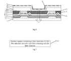
- An embodiment of the present invention provides a method for producing an array substrate disclosed. As illustrated in Fig. 7 , the method includes:
- the array substrate in which the color film and the drain electrode are electrically connected with each other, as shown in Figs. 1-4 may be produced.
- the array substrate provided by the embodiments of the present invention at least has four structures as shown in Figs. 1-4 , that is, the drain electrode of the thin film transistor unit may be on the color film or below the color film, and the thin film transistor unit may be of bottom gate type or be of top gate type.
- the Step S101 in particular includes:
- the thin film transistor unit 2 includes, from the bottom to the top, the gate electrode 21, the gate insulation layer 22 located on the gate electrode 21 and the active layer 23 located on the gate insulation layer 22.
- the gate electrode 21, the gate insulation layer 22 and the active layer 23 are formed sequentially on the array substrate.
- gate electrode of the thin film transistor unit is formed, structures such as gate lines (not shown) on the substrate base are also integrally molded.
- the drain electrode 25 of the thin film transistor unit is located on the active layer 23.
- the thin film transistor unit 2 further includes a source electrode 24.
- the source electrode 24 and the drain electrode 25 of the thin film transistor unit 2 are provided on the same layer. Thus, it may be considered to form the source electrode 24 while forming the drain electrode 25 in the Step S202, as shown in Fig. 10 .
- the source electrode 24 and the drain electrode 25 are arranged in different layers, it may be considered to form the source electrode 24 before or after forming the drain electrode 25.
- the embodiments of the present invention are not limited to this.
- the first insulation layer 6 is formed on the drain electrode of the thin film transistor unit by means such as coating, depositing.
- the first insulation layer 6 is located on the thin film transistor unit 2.
- the first insulation layer 6 is typically called as the passivation layer.
- the process of the passivation layer may not only improve the capacity of environmental resistance for the display apparatus, but also may improve the photo parameter performance of the thin film transistor unit 2.
- the passivation layer typically uses insulation materials such as silicon oxide, silicon nitride, hafnium nitride, resin.
- a layer of masking material is formed on the pattern formed on the first insulation layer 6 by forms of such as coating or depositing, and then a plurality of black matrixes 10 corresponding to the active layers 23 of the respective thin film transistor units 2 are formed by patterning including etching, as shown in Fig. 11 .
- they are preferably made from black photo resist. By means of the photosensitive property of the photo resist, use of the photo resist may be omitted in producing the black matrix 10.
- the black matrix 10 typically covers the entire active layer 23 such that conducting channels formed in the active layer 23 are not irradiated by the light when the thin film transistor unit 2 works.
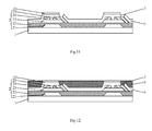
- a first via hole 7 is also provided by patterning in the region corresponding to the drain electrode 25 of the thin film transistor unit 2, as illustrated in Fig. 11 , such that the color film 3 and the drain electrode 25 can be connected efficiently with each other.
- the first insulation layer 6 may be made from insulation materials such as silicon oxide, silicon nitride, hafnium nitride, resin, it may preferably be made from photo resist because the first insulation layer 6 may be patterned to form the first via hole 7. By means of the photosensitive property of the photo resist, use of the photo resist may be omitted in producing the first via hole 7.
- the color film is formed on the drain electrode of the resultant thin film transistor unit.
- the color film 3 may be electrically connected with the drain electrode 25 of the thin film transistor unit 2 through the first via hole 7 of the first insulation layer 6.
- the color film 3 is made from the transparent conductive resin.
- the transparent conductive resin may be produced by the following method:
- the transparent conductive resin After the transparent conductive resin has been prepared, it only needs to dope the corresponding pigments into it, that is, the color film may be formed by the transparent conductive resin with pigments.
- the transparent conductive resin for producing the color film 3 may be produced by mixing nanoscale conductive particles and pigments, light initiator, high molecular polymer monomer, dispersant agent, surface active agent and so on and then by such as coating or depositing means.
- the conductive particles may be nanoscale conductive particles such as nanoscale ITO or nano-silver.
- the array substrate shown in Fig. 1 is an array substrate in a COA-processed twisted nematic (TN) mode display panel.
- the array substrate shown in Fig. 1 may be improved, for example, as illustrated in Fig. 5 , the array substrate further includes a common electrode 13 cooperating with the color film 3 and a third insulation layer 11 between the color film 3 and the common electrode 13 on basis of the array substrate shown in Fig. 1 .
- the array substrate is an array substrate in a COA-processed advanced super dimension switch (ADS) mode display panel.
- ADS advanced super dimension switch
- the array substrate in an organic light-emitting diode (OLED) display panel is formed on the basis of technical solution shown in Fig. 1 .
- the Step S205 then further includes:
- the second insulation layer 8 may be made from insulation materials such as silicon oxide, silicon nitride, hafnium nitride, resin. However, it may preferably be made from photo resist because the second insulation layer 8 may be patterned to form the first via hole 7. By means of the photosensitive property of the photo resist, use of the photo resist may be omitted in producing the opening 9.
- the region to which the opening 9 corresponds is a light emitting region of the array substrate when it works.
- the second insulation layer 8 remained around the opening 9 is a non-luminous region, as illustrated in Fig. 14 . Therefore, the second insulation layer 8 is typically called as a pixel definition layer.
- Step S302 the structure of the array substrate is illustrated in Fig. 15 .
- the organic layer 4 may include a light emitting layer, may further comprise such as a cavity transmission layer, an electron transmission layer.
- a light emitting layer may further comprise such as a cavity transmission layer, an electron transmission layer.
- the positive cavities in the cavity transmission layer bonds to the negative charges in the electron transmission layer in the light emitting layer such that the light emitting layer can produce luminance.
- the electron transmission layer and the cavity transmission layer of the organic light emitting diode may be made from different organic materials or organic materials doped with different impurities.
- the materials that are often used to produce the electron transmission layer have high stability for producing films, high thermal stability and good electron transmission performance.
- the materials may be florescence dye compound, such as anthradiazole-based derivative, naphthalene-ring contianing derivative, 1-naphthyl, 3-methylphenyl.
- the material of the cavity transmission layer belongs to aromatic amine florescence compound, such as organic materials, e.g., 1-naphthyl.
- the material of the light emitting layer of the organic layer 4 must have the properties of strong florescence in solid state, good carrier transmission, thermal stability and chemical stability and high quantum efficiency and can be processed by vacuum vapor plating, for example, may be octohydroxy-quinolinato aluminium.
- the light emitting layer may emit a white light.
- Step S303 of forming a conductive layer on the organic layer is Step S303 of forming a conductive layer on the organic layer.
- the conductive layer 5 is formed by for example vapor plating or sputtering means.
- the conductive layer 5 driving the organic layer 4 to emit the light in combination with the color film 3 is made from opaque material with low costs and a smooth surface. It may prevent the light emitted from the organic layer 4 from exiting one side of the conductive layer 5 and avoid the reduction of utilization coefficient of light by the array substrate.
- the conductive layer is preferably made from white metal having a smooth surface, such as aluminum. It may prevent the light emitted from the organic layer 4 from producing color change after being reflected by the conductive layer 5 such that the display apparatus can have a desired display effect.
- the color film in the array substrate produced by the method is made from transparent conductive resin.
- the color film in combination with the conductive layer drives the organic layer to emit the light.
- the layer of metal anode may be omitted.
- the planarization layer between the metal anode and the color film in the prior art may also be omitted.
- the layer arrangement of the array substrate may be simplified significantly. And as the layer arrangement of the array substrate is simplified, its processing flows and processing difficulty will be reduced, so as to improve the production yield of the array substrate.
- the array substrate shown in Fig. 2 is distinguished from that shown in Fig. 1 in that the thin film transistor unit 2 in Fig. 2 is of top gate type.
- the steps for producing the array substrate shown in Fig. 2 may be derived as follows:
- the first insulation layer 6 is formed on the thin film transistor unit 2 and a black matrix 10 is formed on the first insulation layer 6 corresponding to the active layer 23.
- the first via hole 7 is formed on the first insulation layer 6 and the gate insulation layer 22.
- the colored transparent conductive resin forms the conductive color film 3.
- the first via hole 7 is also filled with the color film such that the color film may be electrically connected with the drain electrode 25.
- the array substrate shown in Fig. 2 may be formed.
- the color films 3 are both located on the drain electrode 25. Similarly, it may be considered to use the producing method in a different order such that the color film 3 is located below the drain electrode 25.
- the color film 3 is formed on the substrate base, and the first insulation layer 6 is formed on the color film 3. Then, the pattern including the drain electrode 25 of the thin film transistor unit 2 may be formed on the color film 3.
- the color film 3 is made from the transparent conductive resin and electrically connected with the drain electrode 25 of the thin film transistor unit 2.
- the method for producing the thin film transistor unit 2 shown in Fig. 3 is similar to that for producing the thin film transistor unit 2 shown in Fig. 1 .
- the details will be omitted below.
- the gate insulation layer 22 and the first insulation layer 6 should be patterned, before the drain electrode 25 is formed, to form the first via hole 7 passing through the gate insulation layer 22 and the first insulation layer 6, and then the first via hole 7 is filled with the material of the drain electrode 25 when the drain electrode 25 is formed, so as to achieve the contact between the drain electrode 25 and the color film 3.
- the color film 3 in Fig. 4 is also located below the drain electrode 25 of the thin film transistor unit 2. And the array substrate in Fig. 4 must also be formed with the color film 3 at first, and then the pattern including the drain electrode 25 of the thin film transistor unit 2 is formed to achieve the contact between the color film 3 and the drain electrode 25.
- the thin film transistor unit 2 in Fig. 4 is of top gate type.
- the method for producing the thin film transistor unit 2 in Fig. 4 is similar to Fig. 2 . The details will be omitted below.
- the first via hole 7 needs to be formed on the first insulation layer 6 after the first insulation layer 6 is formed on the color film 3 such that the drain electrode 25 is in contact with the color film 3 while the drain electrode 25 is produced.
- the common electrode 13 cooperating with the color film 3 and the third insulation layer 11 between the color film 3 and the common electrode 13 may be added on the array substrates shown in the Figs. 2-4 . It may also form the ADS mode array substrate.
- the structures for example the second insulation layer 8, the organic layer 4 and the conductive layer 5 may be added on the array substrates shown in the Figs. 2-4 , so as to form the OLED mode array substrate. The details will be omitted.
Landscapes
- Engineering & Computer Science (AREA)
- Microelectronics & Electronic Packaging (AREA)
- Electroluminescent Light Sources (AREA)
- Devices For Indicating Variable Information By Combining Individual Elements (AREA)
Abstract
Description
- The present disclosure relates to the technical field of display, more particularly, relates to an array substrate, a method for producing the array substrate and a display apparatus.
- An organic light emitting diode (OLED) is an organic thin film electroluminescent device, which has advantages such as simple production process, low costs, high light emitting efficiency, easy production of flexible structures, wide views. Thus, the display technology for the organic light emitting diode has been one important display technology.
- As the technology for white organic light emitting diode (WOLED) has refined and has a good stability and simple production process, it has been widely applied in display apparatuses. In order to achieve colored display of the WOLED, a color film (also called as a color filter) is needed. In a WOLED display apparatus, each of the minimum pixel points that are visible from the external (that is, "visible pixels") is composed of a plurality of pixel units. Each of the pixels has a color film with different colors such that the lights emitted from the WOLED for different pixel units can have different colors through the color film. These lights with different colors may be mixed into the light emitted from the visible pixel.
- The inventors have discovered that the WOLED comprises a metal anode, a conductive layer, an organic light emitter between the metal anode and the conductive layer. Thus, in addition to various layers of a thin film transistor, an array substrate further comprises various layers of the WOLED and the color film. However, it may increase the complication of arrangement of layers of the array substrate and difficulty for producing the array substrate and reduce the yield of the array substrate.
- The object of the present invention is to solve at least one aspect of the above issues and defects in the prior art.
- The technical problem of the present invention is to provide an array substrate and a method for producing the same and a display apparatus that may simplify the layer arrangements and producing process of the array substrate, reduce the difficulty for producing the array substrate and improve the product yield of the array substrate.
- In order to achieve the above object, the present invention may be implemented as the following embodiments.
- According to the first aspect of the present disclosure, it provides an array substrate, comprising: a substrate base; and a thin film transistor unit and a color film on the substrate base, wherein the color film is conductive and electrically connected with a drain electrode of the thin film transistor unit.
- According to an exemplified embodiment, the array substrate may further comprise: a first insulation layer between the color film and the drain electrode of the thin film transistor unit, wherein a first via hole is formed in a region of the first insulation layer corresponding to the drain electrode of the thin film transistor unit, and wherein the color film is electrically connected with the drain electrode through the first via hole.
- According to another exemplified embodiment, the array substrate may further comprise: an organic layer and a conductive layer on the color film, wherein the color film in combination with the conductive layer drives the organic layer to emit a light.
- According to another exemplified embodiment, the array substrate may further comprise: a second insulation layer on the color film, wherein the second insulation layer is provided with an opening thereon, the organic layer being electrically connected with the color film through the opening.
- According to another exemplified embodiment, the array substrate may further comprise: a common electrode cooperating with the color film; and a third insulation layer between the color film and the common electrode.
- According to another exemplified embodiment, the color film is made from transparent conductive material.
- According to another exemplified embodiment, the color film is made of transparent conductive resin.
- According to another exemplified embodiment, the color film is separated electrically into a plurality of parts corresponding to pixel units respectively.
- According to another exemplified embodiment, the plurality of parts of the color film corresponding to pixel units respectively are insulated electrically by an insulation layer.
- According to another exemplified embodiment, the insulation layer is a black matrix.
- In the technical solutions of the embodiment of the present invention, by means of the COA technology, the color film and the thin film transistor unit are both on the same substrate base and the conductive color film is electrically connected with the drain electrode of the thin film transistor unit such that the color film is equivalent to the pixel electrode in the prior art. In this way, the array substrate at least removes a layer of pixel electrode compared with the one in the prior art. It may simplify the layer arrangement of the array substrate, reduce the difficulty of producing the array substrate and further improve the yield of the array substrate.
- The second aspect of the present invention provides a display apparatus comprising an array substrate as described above.
- The third aspect of the present invention provides a method for producing an array substrate, comprising: forming a pattern comprising a drain electrode of a thin film transistor unit and a conductive color film electrically connected with the drain electrode.
- According to an exemplified embodiment, forming a pattern comprising a drain electrode of a thin film transistor unit and a conductive color film electrically connected with the drain electrode comprises: forming the pattern comprising the drain electrode of the thin film transistor unit; and forming the color film on the formed drain electrode of the thin film transistor unit, the color film being electrically connected with the drain electrode of the thin film transistor unit.
- According to another exemplified embodiment, forming a pattern comprising a drain electrode of a thin film transistor unit and a conductive color film electrically connected with the drain electrode comprises: forming the color film; and forming the pattern comprising the drain electrode of the thin film transistor unit on the color film, the color film being electrically connected with the drain electrode of the thin film transistor unit.
- According to another exemplified embodiment, the method further comprise, before forming the color film on the drain electrode of the thin film transistor unit, forming a first insulation layer on the formed drain electrode of the thin film transistor unit and forming a first via hole in a region of the first insulation layer corresponding to the drain electrode of the thin film transistor unit, wherein the color film is electrically connected with the drain electrode through the first via hole.
- According to another exemplified embodiment, the method further comprises, before forming the drain electrode of the thin film transistor unit on the color film, forming a first insulation layer on the color film and forming a first via hole in a region of the first insulation layer corresponding to the drain electrode of the thin film transistor unit, wherein the color film is electrically connected with the drain electrode through the first via hole.
- According to another exemplified embodiment, the method further comprises: forming an organic layer on the formed color film and forming a conductive layer on the organic layer, wherein the color film contacts with the organic layer, and wherein the color film drives the organic layer to emit a light in combination with the conductive layer.
- According to another exemplified embodiment, the method further comprises, before forming the organic layer on the color film, forming a second insulation layer on the color film and forming an opening on the second insulation layer, wherein the organic layer is electrically connected with the color film through the opening.
- The above and other features of the present invention will become more apparent by describing in detail exemplary embodiments thereof with reference to the accompanying drawings. The skilled person in the art would appreciate that the following drawings only shows some embodiments of the present invention, but the present invention is not limited to these drawings by any way.
-
Fig.1 is a first schematic view of a structure of an array substrate according to an embodiment of the present invention; -
Fig.2 is a second schematic view of a structure of an array substrate according to an embodiment of the present invention; -
Fig.3 is a third schematic view of a structure of an array substrate according to an embodiment of the present invention; -
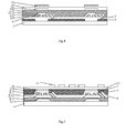
Fig.4 is a fourth schematic view of a structure of an array substrate according to an embodiment of the present invention; -
Fig.5 is a fifth schematic view of a structure of an array substrate according to an embodiment of the present invention; -
Fig.6 is a sixth schematic view of a structure of an array substrate according to an embodiment of the present invention; -
Fig. 7 schematically shows a first flow chart of a method for producing an array substrate according to an embodiment of the present invention; -
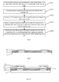
Fig. 8 schematically shows a second flow chart of a method for producing an array substrate according to an embodiment of the present invention; -
Fig.9 is a seventh schematic view of a structure of an array substrate according to an embodiment of the present invention; -
Fig. 10 is an eighth schematic view of a structure of an array substrate according to an embodiment of the present invention; -
Fig.11 is a ninth schematic view of a structure of an array substrate according to an embodiment of the present invention; -
Fig.12 is a tenth schematic view of a structure of an array substrate according to an embodiment of the present invention; -
Fig. 13 schematically shows a third flow chart of a method for producing an array substrate according to an embodiment of the present invention; -
Fig.14 is a eleventh schematic view of a structure of an array substrate according to an embodiment of the present invention; and -
Fig.15 is a twelfth schematic view of a structure of an array substrate according to an embodiment of the present invention. -
- 1--substrate base
- 2--thin film transistor unit
- 21--gate electrode
- 22--gate insulation layer
- 23--active layer
- 24--source electrode
- 25--drain electrode
- 3--color film
- 4--organic layer
- 5--conductive layer
- 6--first insulation layer
- 7--first via hole
- 8--second insulation layer
- 9--opening
- 10--black matrix
- 11--third insulation layer
- 12--fourth insulation layer
- 13--common electrode
- Exemplary embodiments of the present disclosure will be described hereinafter in detail with reference to the attached drawings. Apparently, the disclosed embodiments are only part of those of the present invention, instead of all of embodiments. In view of these embodiments of the present invention, the skilled person in the art may envisage other embodiments without inventive labors. All of the other embodiments also fall within scope of the present invention.
- An embodiment of the present invention provides an array substrate. As illustrated in
Fig. 1 , the array substrate comprises asubstrate base 1 and a thinfilm transistor unit 2 and acolor film 3 on thesubstrate base 1. Thecolor film 3 is electrically connected with adrain electrode 25 of the thinfilm transistor unit 2. Thecolor film 3 is conductive. - The thin
film transistor unit 2 may achieve transmission of electrical signals between itssource electrode 23 anddrain electrode 25 mainly by forming conducting channel in anactive layer 24. However, light irradiation may degrade the capacity of transporting carriers of the conducting channel in the active layer and thus reduce the effects of the working of the thinfilm transistor unit 2. Typically, it is desired to provide ablack matrix 10 corresponding to theactive layer 23 of the thin film transistor unit. - The black matrix may be produced by black or dark resin. In the process producing the
black matrix 10, at first, a layer of masking material is deposited on a passivation layer, and then a plurality ofblack matrixes 10 corresponding to the respective thinfilm transistor units 2 by patterning. In order to simplify the process for producing the array substrate, preferably, the black matrix is made from black photo resist. By means of the photosensitive property of the photo resist, use of the photo resist may be omitted in producing theblack matrix 10. - The patterning means any process that may form a desired pattern. It generally includes part or all of processes of coating the photo resist, exposure, development, etching, peeling off the photo resist, or may be more other patterning means such as printing, pressing.
- As the people is eager to the display apparatus with high performance such as for transmittance, resolution, power assumption recently, the display apparatus is developing towards the objects of such as high transmittance, high resolution, low power assumption. The higher the resolution becomes, the smaller the size of each pixel unit. When the length of each side of the pixel unit becomes between ten and twenty micrometers from dozens of micrometers, obviously, the size of the pixel unit will be reduced significantly. At this time, if the width of black matrix dividing the pixel units is still maintained, the black matrix will become clear with respect to the pixel unit, which may influence the display effects of the display apparatus. Thus, the width of the black matrix should be reduced at a certain extent such that the display apparatus can have a desired display effect. Then, the color film is formed on a display region surrounded by the black matrix corresponding to the pixel unit.
- However, the reduction of width of the black matrix may cause the deviation of alignment between the array substrate and the color film substrate and thus lead to undesired effects, such as light leak. Therefore, the width of the black matrix on the color film substrate cannot be reduced arbitrarily. In order to avoid the undesired effects such as light leak, due to reduction of black matrix, the black matrix and the color film may be moved onto the array substrate. In this way, the black matrix is located on the array substrate, thus, even if the width of the black matrix is reduced slightly, the black matrix can mask the structures that need to be masked, such as gate lines, data lines and thin film transistor unit sufficiently while reducing the probability of light leak. Thus, the display apparatus may have a desired effect while improving resolution and transmittance. Such technology is called as COA(Color Filter on Array) technology.
- In an embodiment of the present invention, the COA technology is used. The
color film 3 and the thinfilm transistor unit 2 are both formed on thesame substrate base 1 and theconductive color film 3 is electrically connected with thedrain electrode 25 of the thinfilm transistor unit 2 such that thecolor film 3 corresponds to the pixel electrode in the prior art. In this way, the array substrate at least removes a layer of pixel electrode compared with the one in the prior art. It may simplify the layer arrangement of the array substrate, reduce the difficulty of producing the array substrate and further improve the yield of the array substrate. - It should be noted that since the
color film 3 in the embodiment of the present invention is conductive, thecolor film 3 between the respective pixel units needs to be insulated. In particular, it may be achieved by an insulatedblack matrix 10 or other means. However, the embodiments of the present invention are not limited by this. In addition, thecolor film 3 and the drain electrode of the thinfilm transistor unit 2 may be in direct contact with each other such that they are electrically connected. Certainly, thecolor film 3 may be located on or below the drain electrode of the thinfilm transistor unit 2. - As illustrated in
Fig. 1 , besides thecolor film 3 and the thinfilm transistor unit 2, the array substrate further includes afirst insulation layer 6 between thecolor film 3 and thedrain electrode 25 of the thinfilm transistor unit 2. A first viahole 7 is formed in a region of thefirst insulation layer 6 corresponding to thedrain electrode 25 of the thinfilm transistor unit 2. Thecolor film 3 is electrically connected with thedrain electrode 25 through the first viahole 7. - Obviously, the thin
film transistor unit 2 in the array substrate illustrated inFig. 1 is bottom gate type, that is, the thinfilm transistor unit 2 includes, from the bottom to the top: agate electrode 21, agate insulation layer 22, asource electrode 24 and thedrain electrode 25 located on the same layer and insulated, and anactive layer 23 connecting thesource electrode 24 with thedrain electrode 25. - In
Fig. 1 , thecolor film 3 is located on the thinfilm transistor unit 2, thus, thefirst insulation layer 6 is located on the thinfilm transistor unit 2. At this time, thefirst insulation layer 6 is often called as a passivation layer. The process of the passivation layer may not only improve the capacity of environmental resistance for the display apparatus, but also may improve the photo parameter performance of the thinfilm transistor unit 2. However, the passivation layer typically uses insulation materials such as silicon oxide, silicon nitride, hafnium nitride, resin. In order to achieve the electrical connection between thecolor film 3 and thedrain electrode 25, the region of thefirst insulation layer 6 corresponding to thedrain electrode 25 of the thinfilm transistor unit 2 may be provided with the first viahole 7 through thefirst insulation layer 6, such that thecolor film 3 can be electrically connected with thedrain electrode 25 through the first viahole 7. - Although the present disclosure explains the embodiments with reference to the bottom gate type thin film transistor, the present invention is not limited to this. For example, the embodiments of the present invention include top gate type thin film transistor. The bottom gate type thin film transistor should be interpreted as a collective term of bottom gate thin film transistors. So called bottom gate thin film transistor is one type thin film transistor in which the gate of the thin film transistor is located below the semiconductor layer of the thin film transistor. On basis of the same ground, the top gate type thin film transistor should be interpreted as a collective term of top gate thin film transistors. So called top gate thin film transistor is one type thin film transistor in which the gate of the thin film transistor is located on the semiconductor layer of the thin film transistor.
- For example, the thin
film transistor unit 2 also may be of top gate type as illustrated inFig. 2 . The top gate type thinfilm transistor unit 2 has the structure which is almost opposite to that of the bottom gate type thin film transistor unit shown inFig. 1 , that is, the top gate type thin film transistor unit includes, from the bottom to the top: asource electrode 24 and thedrain electrode 25 located on the same layer and insulated, anactive layer 23 connecting thesource electrode 24 with thedrain electrode 25, agate insulation layer 22 and agate electrode 21. - In
Fig. 2 , in order to achieve the contact between thecolor film 3 and thedrain electrode 25, a first viahole 7 may provided in the regions of thefirst insulation layer 6 and thegate insulation layer 22 corresponding to thedrain electrode 25 of the thinfilm transistor unit 2. That is, the first viahole 7 in this circumstance needs passes through two insulation layers, i.e., thefirst insulation layer 6 and thegate insulation layer 22 such that thecolor film 3 can be electrically connected with thedrain electrode 25 through the first viahole 7. - It should be noted that in the arrangement of the array substrate in
Fig. 1 or Fig. 2 , thecolor films 3 corresponding to the respective pixel units may be insulated directly by theblack matrix 10, or may be insulated by providing an additional insulation layer on theblack matrix 10. - Further, as illustrated in
Fig. 3 , thecolor film 3 may also be located below the thinfilm transistor unit 2 if the thinfilm transistor unit 2 is of bottom gate type. Obviously, in this case, thedrain electrode 25 of the bottom gate type thinfilm transistor unit 2 is located in the uppermost layer of the entire stack of the thinfilm transistor unit 2. In order to achieve the contact between thedrain electrode 25 and thecolor film 3, the first viahole 7 must at least pass through thefirst insulation layer 6 and thegate insulation layer 22 such that thecolor film 3 and thedrain electrode 25 can be electrically connected with each other. - Or, as illustrated in
Fig. 4 , thecolor film 3 is also located below the thinfilm transistor unit 2 and the thinfilm transistor unit 2 is of top gate type. Obviously, in this circumstance, thedrain electrode 25 of the top gate type thinfilm transistor unit 2 is located in the lowermost layer of the entire stack of the thinfilm transistor unit 2, thus, the first viahole 7 only needs to pass through thefirst insulation layer 6 so as to achieve the electrical connection between thedrain electrode 25 and thecolor film 3. - Obviously, in consideration of difficulty of producing the first via
hole 7, the first viahole 7 in the array substrate shown inFig. 1 orFig. 4 is easy to be produced. However, the array substrate shown inFig. 4 cannot use thefirst insulation layer 6 between thecolor film 3 and the thinfilm transistor unit 2 as the passivation layer as thecolor film 3 is located below the thinfilm transistor unit 2. It must additionally form afourth insulation layer 12 as the passivation layer such that the array substrate shown inFig. 4 has more layers than that shown inFig. 1 . Thus, in an embodiment of the present invention, preferably, the array substrate shown inFig. 1 is used. - Similar to
Fig. 4 , the array substrate shown inFig. 3 also has thefourth insulation layer 12 as the passivation layer. The fourth insulation layers 12 shown inFig. 3 andFig. 4 may be made from insulation materials such as silicon oxide, silicon nitride, hafnium nitride, resin. - Obviously, in the arrangements in
Fig. 3 and inFig. 4 , thefirst insulation layer 6 may be used to insulate thecolor film 3 corresponding to the respective pixel units. - It should be noted that in an embodiment of the present invention, the
source electrode 24 and thedrain electrode 25 of the thinfilm transistor unit 2 are arranged on the same layer and formed by the same patterning process. However, the thinfilm transistor unit 2 with thesource electrode 24 and thedrain electrode 25 arranged in different layers are also suitable to the embodiment of the present invention. - It should be noted that as the arrangements shown in
Figs. 1-4 have certain similarity, the array substrate will be described below with reference to the array substrate shown inFig. 1 . - As discussed above, as the
color film 3 is conductive, e.g., made from transparent conductive material and is electrically connected with thedrain electrode 25 of the thinfilm transistor unit 2, thecolor film 3 also corresponds to the pixel electrode (corresponding to plate electrode) in the prior art. Obviously, the array substrates shown inFigs. 1-4 are COA-processed twisted nematic (TN) mode array substrates. In view of this, the array substrate shown inFig. 1 may be improved, for example, as illustrated inFig. 5 , the array substrate further includes a common electrode 13(corresponding to slit electrode) cooperating with thecolor film 3 and athird insulation layer 11 between thecolor film 3 and thecommon electrode 13 on basis of the array substrate shown inFig. 1 . In this circumstance, the array substrate is a COA-processed advanced super dimension switch (ADS) mode array substrate. - So called advanced super dimension switch, abbreviated as ADS has the following kernel technical feature: forming multidimensional electrical field by an electrical field produced at slit electrode edge in the same plane and an electrical field produced between the slit electrode layer and the plate electrode layer such that the liquid crystal molecules with all of orientations right on the electrodes and between silt electrodes can rotate so as to improve the work efficiency of the liquid crystal and improve the transimissivity efficiency. The advanced super dimension switch may improve image quality of TFT-LCD productions, and have advantages such as high resolution, high transmittance, low power assumpation, wide view, high aperture opening rate, low chromatic aberration and no push Mura. For different applications, the improved ADS includes high transmittance I-ADS, high aperture opening rate H-ADS and high resolution S-ADS, and the like.
- The skilled person in the art would appreciate that the common electrode in the above embodiments may be plate-shaped or slit-shaped. So the pixel electrodes do. Of course, the sequence of the pixel electrode and the common electrode may be reversible, and they may both be slit electrodes.
- Certainly, the array substrate in the embodiment is also suitable for In-Plane Switch (IPS). IPS has the following technical feature: forming a horizontal electrical field produced by a slit common electrode and a slit pixel electrode in the same plane. For example, a part of the conductive color film in the same layer is used as the pixel electrode and another part is used as the common electrode.
- Similarly, the
common electrode 13 cooperating with thecolor film 3 and thethird insulation layer 11 between the color film and thecommon electrode 13 may be added on the array substrate shown inFigs. 2-4 . Or, in additional to the array substrate inFig. 1 , as shown inFig. 6 , the array substrate further includes anorganic layer 4 and a conductive layer 5 on thecolor film 3. Thecolor film 3 drives theorganic layer 4 to emit a light in combination with the conductive layer 5, that is, such array substrate is an organic light emitting diode(OLED) mode array substrate. - In the array substrate shown in
Fig. 6 , as thecolor film 3 is conductive and electrically connected with thedrain electrode 25 of the thinfilm transistor unit 2, that is, thecolor film 3 corresponds to the metal anode of theorganic layer 4 in the prior art. Thus, in the array substrate, the layer of metal anode may be omitted. Meanwhile, the planarization layer between the metal anode and thecolor film 3 in the prior art is also omitted. Thus, the array arrangement of the OLED mode array substrate may be simplified significantly. And as the layer arrangement of the OLED mode array substrate is simplified, its processing flows and processing difficulty will be reduced, so as to improve the production yield of the OLED mode array substrate. - Similarly, the
common electrode 13 located on thecolor film 3 may be added on the array substrate shown inFigs. 2-4 , so as to form ADS mode array substrate. Its details will be omitted below. - Generally, the OLED mode array substrate has a light emitting direction indicated by dashed arrows in
Fig. 6 . The light is emitted from theorganic layer 4 and exits thesubstrate base 1 through the stack arrangement. - The
organic layer 4 may preferably be made from materials that can emit a white light. Thus, in the embodiment of the present invention, the conductive layer 5 driving theorganic layer 4 to emit the light in combination with thecolor film 3 is preferably made from low cost and opaque materials such as aluminium. The light emitted from theorganic layer 4 may be reflected into thecolor film 3 to improve utilization of the light emitted from theorganic layer 4. Also, the light emitted from theorganic layer 4 may be prevented from changing colors after being reflected by the conductive layer such that the display apparatus may have a desired display effect. - In addition, as all of parts on the entire array substrate do not emit the light towards an observer in work, the
second insulation layer 8 may be provided on the region which does not need to emit the light (for example, the region corresponding to the thinfilm transistor unit 2, overlaying region of the black matrix 10) on thecolor film 3 to insulate thecolor film 3 from theorganic layer 4 such that theorganic layer 4 on the region can be prevented from emitting the light. In contrast, in the region that needs to emit the light, that is, the sub-pixel region, an opening 9 is provided on thesecond insulation layer 8 such that theorganic layer 4 can contact with thecolor film 3 though the opening 9. Since thesecond insulation layer 8 may define the light exiting region, that is, define the sub-pixel region, thesecond insulation layer 8 is typically called as a pixel definition layer. In this way, the region corresponding to the opening 9 is a light emitting region while the region overlaid by thesecond insulation layer 8 does not emit the light. - Similar to the
first insulation layer 6 and thethird insulation layer 11, thesecond insulation layer 8 may also be made from insulation materials such as silicon oxide, silicon nitride, hafnium nitride, resin. - In an embodiment of the present invention, the
color film 3 not only needs good conductive effects, but also needs properties such as relatively high color gamut, phototonus, solidification, transmittance. For example, when the color film is used as an OLED anode, it not only meets the requirement of transmittance (or filtering), but also has a work function matched with the organic layer. Therefore, thecolor film 3 is preferably made from the transparent conductive resin. - The transparent conductive resin should be interpreted as a collective term of the resin having properties of light transmission (or light filtering) and conduction. For example, pigments with corresponding colors are doped in the process of producing the transparent conductive resin, or conductive materials are doped in the process of producing the color film resin. Specifically, the transparent conductive resin may be produced by the following steps:
- adding 10~50 phr transparent base resin and 1~20 phr polyaniline doped with organic acid into 40~90 phr toluene and mixing them to be solved completely to form the transparent conductive resin;
- or adding 10~50 phr transparent base resin, 1~20 phr polyaniline doped with organic acid and 1~15 phr crosslinking monomer into 40~90 phr toluene and mixing them to be solved completely to form the transparent conductive resin;
- or adding 10~50 phr transparent base resin, 1~20 phr polyaniline doped with organic acid, 1~15 phr crosslinking monomer and 0.1~1 phr solidifying initiator into 40~90 phr toluene and mixing them to be solved completely to form the transparent conductive resin.
- After the transparent conductive resin has been prepared, it only needs to dope the corresponding pigments into it, that is, the color film may be formed by the transparent conductive resin with pigments.
- Alternatively, the transparent conductive resin for producing the
color film 3 may be produced by mixing nanoscale SnO2 doped with antimony with pigments, light initator, high molecular polymer monomer, dispersant agent, surface active agent and so on. - Besides the nanoscale SnO2 doped with antimony, the conductive particles may be nanoscale conductive particles such as nanoscale ITO or nano-silver. Generally, the conductive particles may have sizes of 20-50nm.
- In addition, the electrical resistivity of the
resultant color film 3 may be changed by regulating the factors such as curing temperature of the resin, sizes of the conductive particles, light irradiation such that thecolor film 3 may provide a good contact between thedrain electrode 25 and theorganic layer 4. - Further, an embodiment of the present invention also provides a display apparatus comprising the array substrate as described in any of the above embodiments. In particular, the display apparatus may be any products or components having display function, for example, a liquid crystal panel, an electronic paper, an OLED panel, a liquid crystal TV, a liquid crystal display, a digital photo frame, a cell phone or a tablet computer.
- An embodiment of the present invention provides a method for producing an array substrate disclosed. As illustrated in
Fig. 7 , the method includes: - Step S101 of forming a pattern comprising a drain electrode of a thin film transistor unit and a conductive color film electrically connected with the drain electrode.
- Thereby, the array substrate in which the color film and the drain electrode are electrically connected with each other, as shown in
Figs. 1-4 , may be produced. In particular, from theabove Embodiment 1, the array substrate provided by the embodiments of the present invention at least has four structures as shown inFigs. 1-4 , that is, the drain electrode of the thin film transistor unit may be on the color film or below the color film, and the thin film transistor unit may be of bottom gate type or be of top gate type. As an example, if it is desired to produce the array substrate shown inFig. 1 , as illustrated inFig. 8 , the Step S101 in particular includes: - Step S201 of forming a pattern comprising a gate electrode, a gate insulation layer and an active layer of the thin film transistor unit sequentially on the substrate base.
- As illustrated in
Fig. 9 , the thinfilm transistor unit 2 includes, from the bottom to the top, thegate electrode 21, thegate insulation layer 22 located on thegate electrode 21 and theactive layer 23 located on thegate insulation layer 22. Thus, in producing the thinfilm transistor unit 2, thegate electrode 21, thegate insulation layer 22 and theactive layer 23 are formed sequentially on the array substrate. - It should be noted that while the gate electrode of the thin film transistor unit is formed, structures such as gate lines (not shown) on the substrate base are also integrally molded.
- Step S202 of forming the pattern comprising the drain electrode of the thin film transistor unit.
- The
drain electrode 25 of the thin film transistor unit is located on theactive layer 23. Besides the on structures such as thegate electrode 21, thegate insulation layer 22, theactive layer 23 and thedrain electrode 25, the thinfilm transistor unit 2 further includes asource electrode 24. In an embodiment of the present invention, thesource electrode 24 and thedrain electrode 25 of the thinfilm transistor unit 2 are provided on the same layer. Thus, it may be considered to form thesource electrode 24 while forming thedrain electrode 25 in the Step S202, as shown inFig. 10 . - If the
source electrode 24 and thedrain electrode 25 are arranged in different layers, it may be considered to form thesource electrode 24 before or after forming thedrain electrode 25. The embodiments of the present invention are not limited to this. - Step S203 of forming a first insulation layer on the formed drain electrode of the thin film transistor unit.
- Based on the
Fig. 10 corresponding to the Step S202, thefirst insulation layer 6 is formed on the drain electrode of the thin film transistor unit by means such as coating, depositing. Thus, thefirst insulation layer 6 is located on the thinfilm transistor unit 2. In this case, thefirst insulation layer 6 is typically called as the passivation layer. The process of the passivation layer may not only improve the capacity of environmental resistance for the display apparatus, but also may improve the photo parameter performance of the thinfilm transistor unit 2. However, the passivation layer typically uses insulation materials such as silicon oxide, silicon nitride, hafnium nitride, resin. - Step S204 of forming a pattern comprising a black matrix on the first insulation layer, the black matrix being arranged corresponding to the active layer of the thin film transistor unit.
- A layer of masking material is formed on the pattern formed on the
first insulation layer 6 by forms of such as coating or depositing, and then a plurality ofblack matrixes 10 corresponding to theactive layers 23 of the respective thinfilm transistor units 2 are formed by patterning including etching, as shown inFig. 11 . In order to simplify the process of producing the array substrate, they are preferably made from black photo resist. By means of the photosensitive property of the photo resist, use of the photo resist may be omitted in producing theblack matrix 10. - It should be noted that the
black matrix 10 typically covers the entireactive layer 23 such that conducting channels formed in theactive layer 23 are not irradiated by the light when the thinfilm transistor unit 2 works. - Further, after the
black matrix 10 has been formed, a first viahole 7 is also provided by patterning in the region corresponding to thedrain electrode 25 of the thinfilm transistor unit 2, as illustrated inFig. 11 , such that thecolor film 3 and thedrain electrode 25 can be connected efficiently with each other. Although thefirst insulation layer 6 may be made from insulation materials such as silicon oxide, silicon nitride, hafnium nitride, resin, it may preferably be made from photo resist because thefirst insulation layer 6 may be patterned to form the first viahole 7. By means of the photosensitive property of the photo resist, use of the photo resist may be omitted in producing the first viahole 7. - Step S205 of forming the color film on the formed drain electrode of the thin film transistor unit, the color film being electrically connected with the drain electrode of the thin film transistor unit.
- As illustrated in
Fig. 12 , based on the Step S204, the color film is formed on the drain electrode of the resultant thin film transistor unit. Thecolor film 3 may be electrically connected with thedrain electrode 25 of the thinfilm transistor unit 2 through the first viahole 7 of thefirst insulation layer 6. - In order to ensure that the
color film 3 not only has good conducting performance, but also has properties such as relatively high color gamut, phototonus, solidification, transmittance. In an embodiment of the present invention, preferably, thecolor film 3 is made from the transparent conductive resin. In particular, the transparent conductive resin may be produced by the following method: - adding 10∼50 phr transparent base resin and 1∼20 phr polyaniline doped with organic acid into 40∼90 phr toluene and mixing them to be solved completely to form the transparent conductive resin;
- or adding 10∼50 phr transparent base resin, 1∼20 phr polyaniline doped with organic acid and 1∼15 phr crosslinking monomer into 40∼90 phr toluene and mixing them to be solved completely to form the transparent conductive resin;
- or adding 10∼50 phr transparent base resin, 1∼20 phr polyaniline doped with organic acid, 1∼15 phr crosslinking monomer and 0.1∼1 phr solidifying initiator into 40∼90 phr toluene and mixing them to be solved completely to form the transparent conductive resin.
- After the transparent conductive resin has been prepared, it only needs to dope the corresponding pigments into it, that is, the color film may be formed by the transparent conductive resin with pigments.
- As an example, the transparent conductive resin for producing the
color film 3 may be produced by mixing nanoscale conductive particles and pigments, light initiator, high molecular polymer monomer, dispersant agent, surface active agent and so on and then by such as coating or depositing means. - Besides the nanoscale SnO2 doped with antimony, the conductive particles may be nanoscale conductive particles such as nanoscale ITO or nano-silver.
- As discussed above, as the
color film 3 is connected with thedrain electrode 25 of the thinfilm transistor unit 2 and made from the transparent conductive material, thecolor film 3 is equivalent to the pixel electrode in the prior art. Obviously, the array substrate shown inFig. 1 is an array substrate in a COA-processed twisted nematic (TN) mode display panel. In view of this, the array substrate shown inFig. 1 may be improved, for example, as illustrated inFig. 5 , the array substrate further includes acommon electrode 13 cooperating with thecolor film 3 and athird insulation layer 11 between thecolor film 3 and thecommon electrode 13 on basis of the array substrate shown inFig. 1 . In this circumstance, the array substrate is an array substrate in a COA-processed advanced super dimension switch (ADS) mode display panel. - Further, the array substrate in an organic light-emitting diode (OLED) display panel is formed on the basis of technical solution shown in
Fig. 1 . In particular, as shown inFig. 13 , the Step S205 then further includes: - Step S301 of forming a second insulation layer on the color film, the second insulation layer being provided with an opening such that the organic layer is electrically connected with the color film through the opening.
- Similar to the
first insulation layer 6, thesecond insulation layer 8 may be made from insulation materials such as silicon oxide, silicon nitride, hafnium nitride, resin. However, it may preferably be made from photo resist because thesecond insulation layer 8 may be patterned to form the first viahole 7. By means of the photosensitive property of the photo resist, use of the photo resist may be omitted in producing the opening 9. - In an embodiment of the present invention, the region to which the opening 9 corresponds is a light emitting region of the array substrate when it works. Meanwhile, the
second insulation layer 8 remained around the opening 9 is a non-luminous region, as illustrated inFig. 14 . Therefore, thesecond insulation layer 8 is typically called as a pixel definition layer. - Step S302 of forming an organic layer on the color film and forming a conductive layer on the organic layer such that the color film contacts with the organic layer to drive the organic layer to emit the light in combination with the conductive layer.
- After the Step S302, the structure of the array substrate is illustrated in
Fig. 15 . - In particular, the
organic layer 4 may include a light emitting layer, may further comprise such as a cavity transmission layer, an electron transmission layer. For example, when a voltage between thecolor film 3 and the conductive layer 5 is suitable, the positive cavities in the cavity transmission layer bonds to the negative charges in the electron transmission layer in the light emitting layer such that the light emitting layer can produce luminance. - It should be noted that organic materials suitable for transmitting electrons may not be used to transmit cavities. Thus, the electron transmission layer and the cavity transmission layer of the organic light emitting diode may be made from different organic materials or organic materials doped with different impurities. At present, the materials that are often used to produce the electron transmission layer have high stability for producing films, high thermal stability and good electron transmission performance. Typically, the materials may be florescence dye compound, such as anthradiazole-based derivative, naphthalene-ring contianing derivative, 1-naphthyl, 3-methylphenyl. However, the material of the cavity transmission layer belongs to aromatic amine florescence compound, such as organic materials, e.g., 1-naphthyl.
- The material of the light emitting layer of the
organic layer 4 must have the properties of strong florescence in solid state, good carrier transmission, thermal stability and chemical stability and high quantum efficiency and can be processed by vacuum vapor plating, for example, may be octohydroxy-quinolinato aluminium. - In a preferable example, the light emitting layer may emit a white light.
- Step S303 of forming a conductive layer on the organic layer.
- On the array substrate shown in
Fig. 15 , the conductive layer 5 is formed by for example vapor plating or sputtering means. In an embodiment of the present invention, the conductive layer 5 driving theorganic layer 4 to emit the light in combination with thecolor film 3 is made from opaque material with low costs and a smooth surface. It may prevent the light emitted from theorganic layer 4 from exiting one side of the conductive layer 5 and avoid the reduction of utilization coefficient of light by the array substrate. - Further, if the light emitted from the
organic layer 4 is white, the conductive layer is preferably made from white metal having a smooth surface, such as aluminum. It may prevent the light emitted from theorganic layer 4 from producing color change after being reflected by the conductive layer 5 such that the display apparatus can have a desired display effect. - The color film in the array substrate produced by the method is made from transparent conductive resin. The color film in combination with the conductive layer drives the organic layer to emit the light. Thus, in the array substrate, the layer of metal anode may be omitted. Meanwhile, the planarization layer between the metal anode and the color film in the prior art may also be omitted. Thus, the layer arrangement of the array substrate may be simplified significantly. And as the layer arrangement of the array substrate is simplified, its processing flows and processing difficulty will be reduced, so as to improve the production yield of the array substrate.
- Further, from the method for producing the array substrate shown in
Fig. 8 , other methods for producing the array substrates shown inFigs. 2-4 may be derived as follows. - As an example, the array substrate shown in
Fig. 2 is distinguished from that shown inFig. 1 in that the thinfilm transistor unit 2 inFig. 2 is of top gate type. Thus, from the producing steps shown inFig. 8 , the steps for producing the array substrate shown inFig. 2 may be derived as follows: - The top gate type thin
film transistor unit 2 has a structure almost in opposite to the bottom gate type thin film transistor unit shown inFig. 1 , that is, the top gate type thinfilm transistor unit 2 includes, from the bottom to the top: asource electrode 24 and thedrain electrode 25 located on the same layer and insulated to each other, anactive layer 23 connecting thesource electrode 24 with thedrain electrode 25, agate insulation layer 22 and agate electrode 21. Thus, the respective structures of the thinfilm transistor unit 2 including such as thedrain electrode 25, thesource electrode 24, the active layer 233, thegate insulation layer 22 and thegate electrode 21 need to be formed at first on thesubstrate base 1. Similarly, thedrain electrode 25 and thesource electrode 24 may be formed in the same layer or in different layers. - Then, the
first insulation layer 6 is formed on the thinfilm transistor unit 2 and ablack matrix 10 is formed on thefirst insulation layer 6 corresponding to theactive layer 23. Then, in order that thecolor film 3 can be electrically connected with thedrain electrode 25 located at the bottom layer, the first viahole 7 is formed on thefirst insulation layer 6 and thegate insulation layer 22. Finally, the colored transparent conductive resin forms theconductive color film 3. Meanwhile, the first viahole 7 is also filled with the color film such that the color film may be electrically connected with thedrain electrode 25. To this end, the array substrate shown inFig. 2 may be formed. - Obviously, as illustrated in
Figs. 1-2 , thecolor films 3 are both located on thedrain electrode 25. Similarly, it may be considered to use the producing method in a different order such that thecolor film 3 is located below thedrain electrode 25. - As an example, as illustrated in
Fig. 3 , at first, thecolor film 3 is formed on the substrate base, and thefirst insulation layer 6 is formed on thecolor film 3. Then, the pattern including thedrain electrode 25 of the thinfilm transistor unit 2 may be formed on thecolor film 3. Thecolor film 3 is made from the transparent conductive resin and electrically connected with thedrain electrode 25 of the thinfilm transistor unit 2. - Obviously, as the thin
film transistor unit 2 is of bottom gate type in this case, the method for producing the thinfilm transistor unit 2 shown inFig. 3 is similar to that for producing the thinfilm transistor unit 2 shown inFig. 1 . The details will be omitted below. It should be noted that, however, in order that thedrain electrode 25 and thecolor film 3 may contact with each other, thegate insulation layer 22 and thefirst insulation layer 6 should be patterned, before thedrain electrode 25 is formed, to form the first viahole 7 passing through thegate insulation layer 22 and thefirst insulation layer 6, and then the first viahole 7 is filled with the material of thedrain electrode 25 when thedrain electrode 25 is formed, so as to achieve the contact between thedrain electrode 25 and thecolor film 3. - Similar to
Fig. 3 , thecolor film 3 inFig. 4 is also located below thedrain electrode 25 of the thinfilm transistor unit 2. And the array substrate inFig. 4 must also be formed with thecolor film 3 at first, and then the pattern including thedrain electrode 25 of the thinfilm transistor unit 2 is formed to achieve the contact between thecolor film 3 and thedrain electrode 25. Different fromFig. 3 , the thinfilm transistor unit 2 inFig. 4 is of top gate type. Thus, the method for producing the thinfilm transistor unit 2 inFig. 4 is similar toFig. 2 . The details will be omitted below. However, it should be noted that in the step for producing the array substrate inFig. 4 , the first viahole 7 needs to be formed on thefirst insulation layer 6 after thefirst insulation layer 6 is formed on thecolor film 3 such that thedrain electrode 25 is in contact with thecolor film 3 while thedrain electrode 25 is produced. - Similarly, the
common electrode 13 cooperating with thecolor film 3 and thethird insulation layer 11 between thecolor film 3 and thecommon electrode 13 may be added on the array substrates shown in theFigs. 2-4 . It may also form the ADS mode array substrate. - Further, similar to the steps shown in
Fig. 12 , the structures for example thesecond insulation layer 8, theorganic layer 4 and the conductive layer 5 may be added on the array substrates shown in theFigs. 2-4 , so as to form the OLED mode array substrate. The details will be omitted. - Although several exemplary embodiments have been shown and described as above, the present invention is not limited to those and it would be appreciated by those skilled in the art that various changes or modifications may be made in these embodiments within the technical scope of the present disclosure. These changes or modifications will fall within the scope of the present invention. The scope of the present invention is defined in the claims and their equivalents.
Claims (18)
- An array substrate, comprising:a substrate base; anda thin film transistor unit and a color film on the substrate base,wherein the color film is conductive and electrically connected with a drain electrode of the thin film transistor unit.
- The array substrate according to claim 1, further comprising:a first insulation layer between the color film and the drain electrode of the thin film transistor unit,wherein a first via hole is formed in a region of the first insulation layer corresponding to the drain electrode of the thin film transistor unit, andwherein the color film is electrically connected with the drain electrode through the first via hole.
- The array substrate according to claim 2, further comprising:an organic layer and a conductive layer on the color film,wherein the color film in combination with the conductive layer drives the organic layer to emit a light.
- The array substrate according to claim 3, further comprising:a second insulation layer on the color film,wherein the second insulation layer is provided with an opening thereon, the organic layer being electrically connected with the color film through the opening .
- The array substrate according to claim 2, further comprising:a common electrode cooperating with the color film; anda third insulation layer between the color film and the common electrode.
- The array substrate according to any one of claims 1-5, wherein the color film is made from transparent conductive material.
- The array substrate according to claim 6, wherein the color film is made of transparent conductive resin.
- The array substrate according to claim 1, wherein the color film is separated electrically into a plurality of parts corresponding to pixel units respectively.
- The array substrate according to claim 8, wherein the plurality of parts of the color film corresponding to pixel units respectively are insulated electrically by an insulation layer.
- The array substrate according to claim 9, wherein the insulation layer is a black matrix.
- A display apparatus comprising an array substrate according to any one of claims 1-10.
- A method for producing an array substrate, comprising:forming a pattern comprising a drain electrode of a thin film transistor unit and a conductive color film electrically connected with the drain electrode.
- The method according to claim 12, wherein forming a pattern comprising a drain electrode of a thin film transistor unit and a conductive color film electrically connected with the drain electrode comprises:forming the pattern comprising the drain electrode of the thin film transistor unit; andforming the color film on the formed drain electrode of the thin film transistor unit, the color film being electrically connected with the drain electrode of the thin film transistor unit.
- The method according to claim 12, wherein forming a pattern comprising a drain electrode of a thin film transistor unit and a conductive color film electrically connected with the drain electrode comprises:forming the color film; andforming the pattern comprising the drain electrode of the thin film transistor unit on the color film, the color film being electrically connected with the drain electrode of the thin film transistor unit.
- The method according to claim 13, further comprising, before forming the color film on the drain electrode of the thin film transistor unit,
forming a first insulation layer on the formed drain electrode of the thin film transistor unit and forming a first via hole in a region of the first insulation layer corresponding to the drain electrode of the thin film transistor unit,
wherein the color film is electrically connected with the drain electrode through the first via hole. - The method according to claim 14, further comprising, before forming the drain electrode of the thin film transistor unit on the color film,
forming a first insulation layer on the color film and forming a first via hole in a region of the first insulation layer corresponding to the drain electrode of the thin film transistor unit,
wherein the color film is electrically connected with the drain electrode through the first via hole. - The method according to claim 15, further comprising:forming an organic layer on the formed color film and forming a conductive layer on the organic layer,wherein the color film contacts with the organic layer andwherein the color film in combination with the conductive layer drives the organic layer to emit a light.
- The method according to claim 17, further comprising, before forming the organic layer on the color film,
forming a second insulation layer on the color film and forming an opening on the second insulation layer,
wherein the organic layer is electrically connected with the color film through the opening.
Applications Claiming Priority (2)
| Application Number | Priority Date | Filing Date | Title |
|---|---|---|---|
| CN201310741603.2A CN103715204B (en) | 2013-12-27 | 2013-12-27 | Array substrate, manufacturing method thereof and display device |
| PCT/CN2014/075937 WO2015096318A1 (en) | 2013-12-27 | 2014-04-22 | Array substrate, manufacturing method therefor and display device |
Publications (3)
| Publication Number | Publication Date |
|---|---|
| EP2919267A1 true EP2919267A1 (en) | 2015-09-16 |
| EP2919267A4 EP2919267A4 (en) | 2016-07-13 |
| EP2919267B1 EP2919267B1 (en) | 2021-07-28 |
Family
ID=50408042
Family Applications (1)
| Application Number | Title | Priority Date | Filing Date |
|---|---|---|---|
| EP14861126.2A Active EP2919267B1 (en) | 2013-12-27 | 2014-04-22 | Array substrate, manufacturing method therefor and display device |
Country Status (4)
| Country | Link |
|---|---|
| US (1) | US9412797B2 (en) |
| EP (1) | EP2919267B1 (en) |
| CN (1) | CN103715204B (en) |
| WO (1) | WO2015096318A1 (en) |
Families Citing this family (9)
| Publication number | Priority date | Publication date | Assignee | Title |
|---|---|---|---|---|
| CN103700674B (en) * | 2013-12-27 | 2017-02-15 | 京东方科技集团股份有限公司 | Array substrate, preparation method thereof and display device |
| CN103715204B (en) * | 2013-12-27 | 2015-05-27 | 京东方科技集团股份有限公司 | Array substrate, manufacturing method thereof and display device |
| CN106653643B (en) * | 2017-02-22 | 2020-03-17 | 武汉华星光电技术有限公司 | Forming method of test bonding pad and array substrate |
| CN108172694B (en) * | 2017-12-21 | 2020-01-14 | 昆山维信诺科技有限公司 | Display panel and display device |
| CN111554731B (en) * | 2020-06-15 | 2022-06-03 | 京东方科技集团股份有限公司 | OLED display panel preparation method, display panel and display device |
| CN112859455A (en) * | 2021-03-03 | 2021-05-28 | Tcl华星光电技术有限公司 | Display panel and display device |
| CN114442397A (en) * | 2022-01-17 | 2022-05-06 | Tcl华星光电技术有限公司 | Electronic paper, preparation method thereof and electronic device |
| CN114566114B (en) | 2022-04-29 | 2022-08-09 | 惠科股份有限公司 | Display panel and display device |
| CN121398333A (en) * | 2024-07-23 | 2026-01-23 | 苏州思萃新能源光电技术研究所有限公司 | Thin film transistor driving structure and preparation method thereof |
Family Cites Families (12)
| Publication number | Priority date | Publication date | Assignee | Title |
|---|---|---|---|---|
| JPH07503263A (en) * | 1992-02-04 | 1995-04-06 | ネステ オイ | Colored conductive polyaniline formulation |
| US5706064A (en) * | 1995-03-31 | 1998-01-06 | Kabushiki Kaisha Toshiba | LCD having an organic-inorganic hybrid glass functional layer |
| GB9713074D0 (en) * | 1997-06-21 | 1997-08-27 | Cambridge Display Tech Ltd | Electrically-conducting colour filters for use in organic light-emitting displays |
| KR100483988B1 (en) * | 2001-11-29 | 2005-04-15 | 삼성에스디아이 주식회사 | Method of Varying Transmittance in transparent conductive film |
| CN1204628C (en) * | 2003-03-06 | 2005-06-01 | 南开大学 | Organic white-light diode colour dispaly device of active addressing front-set colour film |
| US7294372B2 (en) * | 2003-10-01 | 2007-11-13 | Eastman Kodak Company | Conductive color filters |
| CN101681926A (en) * | 2007-02-28 | 2010-03-24 | 日本瑞翁株式会社 | Active matrix substrate, method for producing the same, and flat display |
| CN201876644U (en) * | 2010-11-23 | 2011-06-22 | 北京京东方光电科技有限公司 | Thin film transistor liquid crystal display panel and liquid crystal display |
| CN102645803B (en) * | 2011-10-17 | 2014-06-18 | 京东方科技集团股份有限公司 | Pixel unit, array substrate, liquid crystal panel, display device and manufacturing methods thereof |
| CN102681276B (en) * | 2012-02-28 | 2014-07-09 | 京东方科技集团股份有限公司 | Array substrate, method for manufacturing same and display device comprising same |
| CN103474578B (en) * | 2013-09-23 | 2016-08-10 | 京东方科技集团股份有限公司 | El light emitting device and preparation method thereof |
| CN103715204B (en) * | 2013-12-27 | 2015-05-27 | 京东方科技集团股份有限公司 | Array substrate, manufacturing method thereof and display device |
-
2013
- 2013-12-27 CN CN201310741603.2A patent/CN103715204B/en active Active
-
2014
- 2014-04-22 EP EP14861126.2A patent/EP2919267B1/en active Active
- 2014-04-22 WO PCT/CN2014/075937 patent/WO2015096318A1/en not_active Ceased
- 2014-04-22 US US14/418,174 patent/US9412797B2/en active Active
Also Published As
| Publication number | Publication date |
|---|---|
| US9412797B2 (en) | 2016-08-09 |
| EP2919267A4 (en) | 2016-07-13 |
| WO2015096318A1 (en) | 2015-07-02 |
| CN103715204A (en) | 2014-04-09 |
| US20150340416A1 (en) | 2015-11-26 |
| EP2919267B1 (en) | 2021-07-28 |
| CN103715204B (en) | 2015-05-27 |
Similar Documents
| Publication | Publication Date | Title |
|---|---|---|
| US9412797B2 (en) | Array substrate with color film | |
| US9484393B2 (en) | Array substrate of a display device, manufacturing method thereof | |
| US9825256B2 (en) | Display panel having a top surface of the conductive layer coplanar with a top surface of the pixel define layer | |
| JP7683096B2 (en) | liquid crystal display device | |
| US9455414B2 (en) | Array substrate, manufacturing method thereof, and display device | |
| US9759966B2 (en) | Array substrate and method of manufacturing the same, and display device | |
| CN109309101B (en) | Display panel and display device | |
| EP3156841A1 (en) | Display base plate, display panel and display device | |
| CN103700683B (en) | Counter substrate of a kind of OLED array and preparation method thereof, display unit | |
| CN110610980A (en) | A display substrate, its preparation method, and a display device | |
| US10263115B2 (en) | Thin film transistor and manufacturing method of the same, array substrate and display device | |
| US20090039448A1 (en) | Thin film transistor, pixel structure and liquid crystal display panel | |
| US12538665B2 (en) | Display substrate and manufacturing method therefor, and display device | |
| US11189816B2 (en) | Display substrate having a unitary cathode layer connected to a plurality of light emitting blocks, display apparatus, and method of fabricating display having the same | |
| US11239293B2 (en) | Array substrate, display panel, display device and method for preparing array substrate | |
| KR20150073388A (en) | Transparent crystal display device | |
| US10483497B2 (en) | OLED substrate and manufacturing method thereof and display device | |
| US9520451B2 (en) | Organic light-emitting diode display device and method of manufacturing the same | |
| WO2019223198A1 (en) | Fabrication method for oled backplate and oled backplate | |
| US12336393B2 (en) | Light-emitting device, substrate thereof and fabrication method | |
| US20060146235A1 (en) | Color filter substrate for liquid crystal display and method of fabricating the same | |
| WO2018171269A1 (en) | Color film substrate, fabrication method thereof, and display device | |
| US20220020830A1 (en) | Patterning of Organic Light Emitting Diode Device and the OLED Displays Manufactured Therefrom | |
| CN115207065A (en) | Display module, preparation method of display module and display device |
Legal Events
| Date | Code | Title | Description |
|---|---|---|---|
| PUAI | Public reference made under article 153(3) epc to a published international application that has entered the european phase |
Free format text: ORIGINAL CODE: 0009012 |
|
| 17P | Request for examination filed |
Effective date: 20150518 |
|
| AK | Designated contracting states |
Kind code of ref document: A1 Designated state(s): AL AT BE BG CH CY CZ DE DK EE ES FI FR GB GR HR HU IE IS IT LI LT LU LV MC MK MT NL NO PL PT RO RS SE SI SK SM TR |
|
| AX | Request for extension of the european patent |
Extension state: BA ME |
|
| RA4 | Supplementary search report drawn up and despatched (corrected) |
Effective date: 20160613 |
|
| RIC1 | Information provided on ipc code assigned before grant |
Ipc: H01L 21/77 20060101ALI20160607BHEP Ipc: H01L 51/52 20060101ALI20160607BHEP Ipc: H01L 27/32 20060101ALI20160607BHEP Ipc: H01L 27/12 20060101AFI20160607BHEP |
|
| DAX | Request for extension of the european patent (deleted) | ||
| STAA | Information on the status of an ep patent application or granted ep patent |
Free format text: STATUS: EXAMINATION IS IN PROGRESS |
|
| 17Q | First examination report despatched |
Effective date: 20180726 |
|
| GRAP | Despatch of communication of intention to grant a patent |
Free format text: ORIGINAL CODE: EPIDOSNIGR1 |
|
| STAA | Information on the status of an ep patent application or granted ep patent |
Free format text: STATUS: GRANT OF PATENT IS INTENDED |
|
| INTG | Intention to grant announced |
Effective date: 20210225 |
|
| GRAS | Grant fee paid |
Free format text: ORIGINAL CODE: EPIDOSNIGR3 |
|
| GRAA | (expected) grant |
Free format text: ORIGINAL CODE: 0009210 |
|
| STAA | Information on the status of an ep patent application or granted ep patent |
Free format text: STATUS: THE PATENT HAS BEEN GRANTED |
|
| AK | Designated contracting states |
Kind code of ref document: B1 Designated state(s): AL AT BE BG CH CY CZ DE DK EE ES FI FR GB GR HR HU IE IS IT LI LT LU LV MC MK MT NL NO PL PT RO RS SE SI SK SM TR |
|
| REG | Reference to a national code |
Ref country code: GB Ref legal event code: FG4D |
|
| REG | Reference to a national code |
Ref country code: CH Ref legal event code: EP |
|
| REG | Reference to a national code |
Ref country code: DE Ref legal event code: R096 Ref document number: 602014079109 Country of ref document: DE |
|
| REG | Reference to a national code |
Ref country code: AT Ref legal event code: REF Ref document number: 1415482 Country of ref document: AT Kind code of ref document: T Effective date: 20210815 |
|
| REG | Reference to a national code |
Ref country code: IE Ref legal event code: FG4D |
|
| REG | Reference to a national code |
Ref country code: LT Ref legal event code: MG9D |
|
| REG | Reference to a national code |
Ref country code: NL Ref legal event code: MP Effective date: 20210728 |
|
| REG | Reference to a national code |
Ref country code: AT Ref legal event code: MK05 Ref document number: 1415482 Country of ref document: AT Kind code of ref document: T Effective date: 20210728 |
|
| PG25 | Lapsed in a contracting state [announced via postgrant information from national office to epo] |
Ref country code: HR Free format text: LAPSE BECAUSE OF FAILURE TO SUBMIT A TRANSLATION OF THE DESCRIPTION OR TO PAY THE FEE WITHIN THE PRESCRIBED TIME-LIMIT Effective date: 20210728 Ref country code: RS Free format text: LAPSE BECAUSE OF FAILURE TO SUBMIT A TRANSLATION OF THE DESCRIPTION OR TO PAY THE FEE WITHIN THE PRESCRIBED TIME-LIMIT Effective date: 20210728 Ref country code: SE Free format text: LAPSE BECAUSE OF FAILURE TO SUBMIT A TRANSLATION OF THE DESCRIPTION OR TO PAY THE FEE WITHIN THE PRESCRIBED TIME-LIMIT Effective date: 20210728 Ref country code: BG Free format text: LAPSE BECAUSE OF FAILURE TO SUBMIT A TRANSLATION OF THE DESCRIPTION OR TO PAY THE FEE WITHIN THE PRESCRIBED TIME-LIMIT Effective date: 20211028 Ref country code: AT Free format text: LAPSE BECAUSE OF FAILURE TO SUBMIT A TRANSLATION OF THE DESCRIPTION OR TO PAY THE FEE WITHIN THE PRESCRIBED TIME-LIMIT Effective date: 20210728 Ref country code: LT Free format text: LAPSE BECAUSE OF FAILURE TO SUBMIT A TRANSLATION OF THE DESCRIPTION OR TO PAY THE FEE WITHIN THE PRESCRIBED TIME-LIMIT Effective date: 20210728 Ref country code: NL Free format text: LAPSE BECAUSE OF FAILURE TO SUBMIT A TRANSLATION OF THE DESCRIPTION OR TO PAY THE FEE WITHIN THE PRESCRIBED TIME-LIMIT Effective date: 20210728 Ref country code: NO Free format text: LAPSE BECAUSE OF FAILURE TO SUBMIT A TRANSLATION OF THE DESCRIPTION OR TO PAY THE FEE WITHIN THE PRESCRIBED TIME-LIMIT Effective date: 20211028 Ref country code: PT Free format text: LAPSE BECAUSE OF FAILURE TO SUBMIT A TRANSLATION OF THE DESCRIPTION OR TO PAY THE FEE WITHIN THE PRESCRIBED TIME-LIMIT Effective date: 20211129 Ref country code: ES Free format text: LAPSE BECAUSE OF FAILURE TO SUBMIT A TRANSLATION OF THE DESCRIPTION OR TO PAY THE FEE WITHIN THE PRESCRIBED TIME-LIMIT Effective date: 20210728 Ref country code: FI Free format text: LAPSE BECAUSE OF FAILURE TO SUBMIT A TRANSLATION OF THE DESCRIPTION OR TO PAY THE FEE WITHIN THE PRESCRIBED TIME-LIMIT Effective date: 20210728 |
|
| PG25 | Lapsed in a contracting state [announced via postgrant information from national office to epo] |
Ref country code: PL Free format text: LAPSE BECAUSE OF FAILURE TO SUBMIT A TRANSLATION OF THE DESCRIPTION OR TO PAY THE FEE WITHIN THE PRESCRIBED TIME-LIMIT Effective date: 20210728 Ref country code: LV Free format text: LAPSE BECAUSE OF FAILURE TO SUBMIT A TRANSLATION OF THE DESCRIPTION OR TO PAY THE FEE WITHIN THE PRESCRIBED TIME-LIMIT Effective date: 20210728 Ref country code: GR Free format text: LAPSE BECAUSE OF FAILURE TO SUBMIT A TRANSLATION OF THE DESCRIPTION OR TO PAY THE FEE WITHIN THE PRESCRIBED TIME-LIMIT Effective date: 20211029 |
|
| PG25 | Lapsed in a contracting state [announced via postgrant information from national office to epo] |
Ref country code: DK Free format text: LAPSE BECAUSE OF FAILURE TO SUBMIT A TRANSLATION OF THE DESCRIPTION OR TO PAY THE FEE WITHIN THE PRESCRIBED TIME-LIMIT Effective date: 20210728 |
|
| REG | Reference to a national code |
Ref country code: DE Ref legal event code: R097 Ref document number: 602014079109 Country of ref document: DE |
|
| PG25 | Lapsed in a contracting state [announced via postgrant information from national office to epo] |
Ref country code: SM Free format text: LAPSE BECAUSE OF FAILURE TO SUBMIT A TRANSLATION OF THE DESCRIPTION OR TO PAY THE FEE WITHIN THE PRESCRIBED TIME-LIMIT Effective date: 20210728 Ref country code: SK Free format text: LAPSE BECAUSE OF FAILURE TO SUBMIT A TRANSLATION OF THE DESCRIPTION OR TO PAY THE FEE WITHIN THE PRESCRIBED TIME-LIMIT Effective date: 20210728 Ref country code: RO Free format text: LAPSE BECAUSE OF FAILURE TO SUBMIT A TRANSLATION OF THE DESCRIPTION OR TO PAY THE FEE WITHIN THE PRESCRIBED TIME-LIMIT Effective date: 20210728 Ref country code: EE Free format text: LAPSE BECAUSE OF FAILURE TO SUBMIT A TRANSLATION OF THE DESCRIPTION OR TO PAY THE FEE WITHIN THE PRESCRIBED TIME-LIMIT Effective date: 20210728 Ref country code: CZ Free format text: LAPSE BECAUSE OF FAILURE TO SUBMIT A TRANSLATION OF THE DESCRIPTION OR TO PAY THE FEE WITHIN THE PRESCRIBED TIME-LIMIT Effective date: 20210728 Ref country code: AL Free format text: LAPSE BECAUSE OF FAILURE TO SUBMIT A TRANSLATION OF THE DESCRIPTION OR TO PAY THE FEE WITHIN THE PRESCRIBED TIME-LIMIT Effective date: 20210728 |
|
| PLBE | No opposition filed within time limit |
Free format text: ORIGINAL CODE: 0009261 |
|
| STAA | Information on the status of an ep patent application or granted ep patent |
Free format text: STATUS: NO OPPOSITION FILED WITHIN TIME LIMIT |
|
| 26N | No opposition filed |
Effective date: 20220429 |
|
| PG25 | Lapsed in a contracting state [announced via postgrant information from national office to epo] |
Ref country code: IT Free format text: LAPSE BECAUSE OF FAILURE TO SUBMIT A TRANSLATION OF THE DESCRIPTION OR TO PAY THE FEE WITHIN THE PRESCRIBED TIME-LIMIT Effective date: 20210728 |
|
| REG | Reference to a national code |
Ref country code: CH Ref legal event code: PL |
|
| GBPC | Gb: european patent ceased through non-payment of renewal fee |
Effective date: 20220422 |
|
| REG | Reference to a national code |
Ref country code: BE Ref legal event code: MM Effective date: 20220430 |
|
| PG25 | Lapsed in a contracting state [announced via postgrant information from national office to epo] |
Ref country code: MC Free format text: LAPSE BECAUSE OF FAILURE TO SUBMIT A TRANSLATION OF THE DESCRIPTION OR TO PAY THE FEE WITHIN THE PRESCRIBED TIME-LIMIT Effective date: 20210728 Ref country code: LU Free format text: LAPSE BECAUSE OF NON-PAYMENT OF DUE FEES Effective date: 20220422 Ref country code: LI Free format text: LAPSE BECAUSE OF NON-PAYMENT OF DUE FEES Effective date: 20220430 Ref country code: GB Free format text: LAPSE BECAUSE OF NON-PAYMENT OF DUE FEES Effective date: 20220422 Ref country code: FR Free format text: LAPSE BECAUSE OF NON-PAYMENT OF DUE FEES Effective date: 20220430 Ref country code: CH Free format text: LAPSE BECAUSE OF NON-PAYMENT OF DUE FEES Effective date: 20220430 |
|
| PG25 | Lapsed in a contracting state [announced via postgrant information from national office to epo] |
Ref country code: BE Free format text: LAPSE BECAUSE OF NON-PAYMENT OF DUE FEES Effective date: 20220430 |
|
| PG25 | Lapsed in a contracting state [announced via postgrant information from national office to epo] |
Ref country code: IE Free format text: LAPSE BECAUSE OF NON-PAYMENT OF DUE FEES Effective date: 20220422 |
|
| PG25 | Lapsed in a contracting state [announced via postgrant information from national office to epo] |
Ref country code: HU Free format text: LAPSE BECAUSE OF FAILURE TO SUBMIT A TRANSLATION OF THE DESCRIPTION OR TO PAY THE FEE WITHIN THE PRESCRIBED TIME-LIMIT; INVALID AB INITIO Effective date: 20140422 |
|
| PG25 | Lapsed in a contracting state [announced via postgrant information from national office to epo] |
Ref country code: MK Free format text: LAPSE BECAUSE OF FAILURE TO SUBMIT A TRANSLATION OF THE DESCRIPTION OR TO PAY THE FEE WITHIN THE PRESCRIBED TIME-LIMIT Effective date: 20210728 Ref country code: CY Free format text: LAPSE BECAUSE OF FAILURE TO SUBMIT A TRANSLATION OF THE DESCRIPTION OR TO PAY THE FEE WITHIN THE PRESCRIBED TIME-LIMIT Effective date: 20210728 |
|
| PG25 | Lapsed in a contracting state [announced via postgrant information from national office to epo] |
Ref country code: TR Free format text: LAPSE BECAUSE OF FAILURE TO SUBMIT A TRANSLATION OF THE DESCRIPTION OR TO PAY THE FEE WITHIN THE PRESCRIBED TIME-LIMIT Effective date: 20210728 |
|
| PG25 | Lapsed in a contracting state [announced via postgrant information from national office to epo] |
Ref country code: MT Free format text: LAPSE BECAUSE OF FAILURE TO SUBMIT A TRANSLATION OF THE DESCRIPTION OR TO PAY THE FEE WITHIN THE PRESCRIBED TIME-LIMIT Effective date: 20210728 |
|
| REG | Reference to a national code |
Ref country code: DE Ref legal event code: R079 Ref document number: 602014079109 Country of ref document: DE Free format text: PREVIOUS MAIN CLASS: H01L0027120000 Ipc: H10D0086000000 |
|
| PGFP | Annual fee paid to national office [announced via postgrant information from national office to epo] |
Ref country code: DE Payment date: 20260427 Year of fee payment: 13 |