EP2919265A2 - Semiconductor package and method for fabricating base for semiconductor package - Google Patents
Semiconductor package and method for fabricating base for semiconductor package Download PDFInfo
- Publication number
- EP2919265A2 EP2919265A2 EP15155491.2A EP15155491A EP2919265A2 EP 2919265 A2 EP2919265 A2 EP 2919265A2 EP 15155491 A EP15155491 A EP 15155491A EP 2919265 A2 EP2919265 A2 EP 2919265A2
- Authority
- EP
- European Patent Office
- Prior art keywords
- base
- semiconductor package
- conductive
- material layer
- base material
- Prior art date
- Legal status (The legal status is an assumption and is not a legal conclusion. Google has not performed a legal analysis and makes no representation as to the accuracy of the status listed.)
- Granted
Links
Images



Classifications
-
- H—ELECTRICITY
- H10—SEMICONDUCTOR DEVICES; ELECTRIC SOLID-STATE DEVICES NOT OTHERWISE PROVIDED FOR
- H10W—GENERIC PACKAGES, INTERCONNECTIONS, CONNECTORS OR OTHER CONSTRUCTIONAL DETAILS OF DEVICES COVERED BY CLASS H10
- H10W70/00—Package substrates; Interposers; Redistribution layers [RDL]
- H10W70/01—Manufacture or treatment
- H10W70/05—Manufacture or treatment of insulating or insulated package substrates, or of interposers, or of redistribution layers
- H10W70/092—Adapting interconnections, e.g. making engineering charges, repairing
-
- H—ELECTRICITY
- H01—ELECTRIC ELEMENTS
- H01F—MAGNETS; INDUCTANCES; TRANSFORMERS; SELECTION OF MATERIALS FOR THEIR MAGNETIC PROPERTIES
- H01F17/00—Fixed inductances of the signal type
-
- H—ELECTRICITY
- H05—ELECTRIC TECHNIQUES NOT OTHERWISE PROVIDED FOR
- H05K—PRINTED CIRCUITS; CASINGS OR CONSTRUCTIONAL DETAILS OF ELECTRIC APPARATUS; MANUFACTURE OF ASSEMBLAGES OF ELECTRICAL COMPONENTS
- H05K1/00—Printed circuits
- H05K1/18—Printed circuits structurally associated with non-printed electric components
- H05K1/181—Printed circuits structurally associated with non-printed electric components associated with surface mounted components
-
- H—ELECTRICITY
- H05—ELECTRIC TECHNIQUES NOT OTHERWISE PROVIDED FOR
- H05K—PRINTED CIRCUITS; CASINGS OR CONSTRUCTIONAL DETAILS OF ELECTRIC APPARATUS; MANUFACTURE OF ASSEMBLAGES OF ELECTRICAL COMPONENTS
- H05K1/00—Printed circuits
- H05K1/18—Printed circuits structurally associated with non-printed electric components
- H05K1/182—Printed circuits structurally associated with non-printed electric components associated with components mounted in printed circuit boards [PCB], e.g. insert-mounted components [IMC]
- H05K1/183—Printed circuits structurally associated with non-printed electric components associated with components mounted in printed circuit boards [PCB], e.g. insert-mounted components [IMC] associated with components mounted in and supported by recessed areas of the PCBs
-
- H—ELECTRICITY
- H05—ELECTRIC TECHNIQUES NOT OTHERWISE PROVIDED FOR
- H05K—PRINTED CIRCUITS; CASINGS OR CONSTRUCTIONAL DETAILS OF ELECTRIC APPARATUS; MANUFACTURE OF ASSEMBLAGES OF ELECTRICAL COMPONENTS
- H05K3/00—Apparatus or processes for manufacturing printed circuits
- H05K3/0011—Working of insulating substrates or insulating layers
- H05K3/0017—Etching of the substrate by chemical or physical means
-
- H—ELECTRICITY
- H05—ELECTRIC TECHNIQUES NOT OTHERWISE PROVIDED FOR
- H05K—PRINTED CIRCUITS; CASINGS OR CONSTRUCTIONAL DETAILS OF ELECTRIC APPARATUS; MANUFACTURE OF ASSEMBLAGES OF ELECTRICAL COMPONENTS
- H05K3/00—Apparatus or processes for manufacturing printed circuits
- H05K3/0011—Working of insulating substrates or insulating layers
- H05K3/0017—Etching of the substrate by chemical or physical means
- H05K3/0026—Etching of the substrate by chemical or physical means by laser ablation
-
- H—ELECTRICITY
- H05—ELECTRIC TECHNIQUES NOT OTHERWISE PROVIDED FOR
- H05K—PRINTED CIRCUITS; CASINGS OR CONSTRUCTIONAL DETAILS OF ELECTRIC APPARATUS; MANUFACTURE OF ASSEMBLAGES OF ELECTRICAL COMPONENTS
- H05K3/00—Apparatus or processes for manufacturing printed circuits
- H05K3/0011—Working of insulating substrates or insulating layers
- H05K3/0044—Mechanical working of the substrate, e.g. drilling or punching
- H05K3/0047—Drilling of holes
-
- H—ELECTRICITY
- H05—ELECTRIC TECHNIQUES NOT OTHERWISE PROVIDED FOR
- H05K—PRINTED CIRCUITS; CASINGS OR CONSTRUCTIONAL DETAILS OF ELECTRIC APPARATUS; MANUFACTURE OF ASSEMBLAGES OF ELECTRICAL COMPONENTS
- H05K3/00—Apparatus or processes for manufacturing printed circuits
- H05K3/10—Apparatus or processes for manufacturing printed circuits in which conductive material is applied to the insulating support in such a manner as to form the desired conductive pattern
- H05K3/107—Apparatus or processes for manufacturing printed circuits in which conductive material is applied to the insulating support in such a manner as to form the desired conductive pattern by filling grooves in the support with conductive material
-
- H—ELECTRICITY
- H05—ELECTRIC TECHNIQUES NOT OTHERWISE PROVIDED FOR
- H05K—PRINTED CIRCUITS; CASINGS OR CONSTRUCTIONAL DETAILS OF ELECTRIC APPARATUS; MANUFACTURE OF ASSEMBLAGES OF ELECTRICAL COMPONENTS
- H05K3/00—Apparatus or processes for manufacturing printed circuits
- H05K3/10—Apparatus or processes for manufacturing printed circuits in which conductive material is applied to the insulating support in such a manner as to form the desired conductive pattern
- H05K3/18—Apparatus or processes for manufacturing printed circuits in which conductive material is applied to the insulating support in such a manner as to form the desired conductive pattern using precipitation techniques to apply the conductive material
- H05K3/188—Apparatus or processes for manufacturing printed circuits in which conductive material is applied to the insulating support in such a manner as to form the desired conductive pattern using precipitation techniques to apply the conductive material by direct electroplating
-
- H—ELECTRICITY
- H05—ELECTRIC TECHNIQUES NOT OTHERWISE PROVIDED FOR
- H05K—PRINTED CIRCUITS; CASINGS OR CONSTRUCTIONAL DETAILS OF ELECTRIC APPARATUS; MANUFACTURE OF ASSEMBLAGES OF ELECTRICAL COMPONENTS
- H05K3/00—Apparatus or processes for manufacturing printed circuits
- H05K3/30—Assembling printed circuits with electric components, e.g. with resistors
- H05K3/303—Assembling printed circuits with electric components, e.g. with resistors with surface mounted components
-
- H—ELECTRICITY
- H10—SEMICONDUCTOR DEVICES; ELECTRIC SOLID-STATE DEVICES NOT OTHERWISE PROVIDED FOR
- H10W—GENERIC PACKAGES, INTERCONNECTIONS, CONNECTORS OR OTHER CONSTRUCTIONAL DETAILS OF DEVICES COVERED BY CLASS H10
- H10W44/00—Electrical arrangements for controlling or matching impedance
- H10W44/20—Electrical arrangements for controlling or matching impedance at high-frequency [HF] or radio frequency [RF]
-
- H—ELECTRICITY
- H10—SEMICONDUCTOR DEVICES; ELECTRIC SOLID-STATE DEVICES NOT OTHERWISE PROVIDED FOR
- H10W—GENERIC PACKAGES, INTERCONNECTIONS, CONNECTORS OR OTHER CONSTRUCTIONAL DETAILS OF DEVICES COVERED BY CLASS H10
- H10W44/00—Electrical arrangements for controlling or matching impedance
- H10W44/501—Inductive arrangements
-
- H—ELECTRICITY
- H10—SEMICONDUCTOR DEVICES; ELECTRIC SOLID-STATE DEVICES NOT OTHERWISE PROVIDED FOR
- H10W—GENERIC PACKAGES, INTERCONNECTIONS, CONNECTORS OR OTHER CONSTRUCTIONAL DETAILS OF DEVICES COVERED BY CLASS H10
- H10W44/00—Electrical arrangements for controlling or matching impedance
- H10W44/601—Capacitive arrangements
-
- H—ELECTRICITY
- H10—SEMICONDUCTOR DEVICES; ELECTRIC SOLID-STATE DEVICES NOT OTHERWISE PROVIDED FOR
- H10W—GENERIC PACKAGES, INTERCONNECTIONS, CONNECTORS OR OTHER CONSTRUCTIONAL DETAILS OF DEVICES COVERED BY CLASS H10
- H10W70/00—Package substrates; Interposers; Redistribution layers [RDL]
- H10W70/01—Manufacture or treatment
- H10W70/05—Manufacture or treatment of insulating or insulated package substrates, or of interposers, or of redistribution layers
- H10W70/095—Manufacture or treatment of insulating or insulated package substrates, or of interposers, or of redistribution layers of vias therein
-
- H—ELECTRICITY
- H10—SEMICONDUCTOR DEVICES; ELECTRIC SOLID-STATE DEVICES NOT OTHERWISE PROVIDED FOR
- H10W—GENERIC PACKAGES, INTERCONNECTIONS, CONNECTORS OR OTHER CONSTRUCTIONAL DETAILS OF DEVICES COVERED BY CLASS H10
- H10W70/00—Package substrates; Interposers; Redistribution layers [RDL]
- H10W70/60—Insulating or insulated package substrates; Interposers; Redistribution layers
- H10W70/611—Insulating or insulated package substrates; Interposers; Redistribution layers for connecting multiple chips together
- H10W70/614—Insulating or insulated package substrates; Interposers; Redistribution layers for connecting multiple chips together the multiple chips being integrally enclosed
-
- H—ELECTRICITY
- H10—SEMICONDUCTOR DEVICES; ELECTRIC SOLID-STATE DEVICES NOT OTHERWISE PROVIDED FOR
- H10W—GENERIC PACKAGES, INTERCONNECTIONS, CONNECTORS OR OTHER CONSTRUCTIONAL DETAILS OF DEVICES COVERED BY CLASS H10
- H10W70/00—Package substrates; Interposers; Redistribution layers [RDL]
- H10W70/60—Insulating or insulated package substrates; Interposers; Redistribution layers
- H10W70/62—Insulating or insulated package substrates; Interposers; Redistribution layers characterised by their interconnections
- H10W70/63—Vias, e.g. via plugs
- H10W70/635—Through-vias
-
- H—ELECTRICITY
- H10—SEMICONDUCTOR DEVICES; ELECTRIC SOLID-STATE DEVICES NOT OTHERWISE PROVIDED FOR
- H10W—GENERIC PACKAGES, INTERCONNECTIONS, CONNECTORS OR OTHER CONSTRUCTIONAL DETAILS OF DEVICES COVERED BY CLASS H10
- H10W72/00—Interconnections or connectors in packages
- H10W72/20—Bump connectors, e.g. solder bumps or copper pillars; Dummy bumps; Thermal bumps
-
- H—ELECTRICITY
- H10—SEMICONDUCTOR DEVICES; ELECTRIC SOLID-STATE DEVICES NOT OTHERWISE PROVIDED FOR
- H10W—GENERIC PACKAGES, INTERCONNECTIONS, CONNECTORS OR OTHER CONSTRUCTIONAL DETAILS OF DEVICES COVERED BY CLASS H10
- H10W90/00—Package configurations
-
- H—ELECTRICITY
- H01—ELECTRIC ELEMENTS
- H01F—MAGNETS; INDUCTANCES; TRANSFORMERS; SELECTION OF MATERIALS FOR THEIR MAGNETIC PROPERTIES
- H01F17/00—Fixed inductances of the signal type
- H01F17/0006—Printed inductances
-
- H—ELECTRICITY
- H05—ELECTRIC TECHNIQUES NOT OTHERWISE PROVIDED FOR
- H05K—PRINTED CIRCUITS; CASINGS OR CONSTRUCTIONAL DETAILS OF ELECTRIC APPARATUS; MANUFACTURE OF ASSEMBLAGES OF ELECTRICAL COMPONENTS
- H05K1/00—Printed circuits
- H05K1/16—Printed circuits incorporating printed electric components, e.g. printed resistors, capacitors or inductors
- H05K1/165—Printed circuits incorporating printed electric components, e.g. printed resistors, capacitors or inductors incorporating printed inductors
-
- H—ELECTRICITY
- H05—ELECTRIC TECHNIQUES NOT OTHERWISE PROVIDED FOR
- H05K—PRINTED CIRCUITS; CASINGS OR CONSTRUCTIONAL DETAILS OF ELECTRIC APPARATUS; MANUFACTURE OF ASSEMBLAGES OF ELECTRICAL COMPONENTS
- H05K2201/00—Indexing scheme relating to printed circuits covered by H05K1/00
- H05K2201/10—Details of components or other objects attached to or integrated in a printed circuit board
- H05K2201/10007—Types of components
- H05K2201/10098—Components for radio transmission, e.g. radio frequency identification [RFID] tag, printed or non-printed antennas
-
- H—ELECTRICITY
- H10—SEMICONDUCTOR DEVICES; ELECTRIC SOLID-STATE DEVICES NOT OTHERWISE PROVIDED FOR
- H10D—INORGANIC ELECTRIC SEMICONDUCTOR DEVICES
- H10D84/00—Integrated devices formed in or on semiconductor substrates that comprise only semiconducting layers, e.g. on Si wafers or on GaAs-on-Si wafers
- H10D84/01—Manufacture or treatment
-
- H—ELECTRICITY
- H10—SEMICONDUCTOR DEVICES; ELECTRIC SOLID-STATE DEVICES NOT OTHERWISE PROVIDED FOR
- H10P—GENERIC PROCESSES OR APPARATUS FOR THE MANUFACTURE OR TREATMENT OF DEVICES COVERED BY CLASS H10
- H10P72/00—Handling or holding of wafers, substrates or devices during manufacture or treatment thereof
- H10P72/70—Handling or holding of wafers, substrates or devices during manufacture or treatment thereof for supporting or gripping
- H10P72/74—Handling or holding of wafers, substrates or devices during manufacture or treatment thereof for supporting or gripping using temporarily an auxiliary support
-
- H—ELECTRICITY
- H10—SEMICONDUCTOR DEVICES; ELECTRIC SOLID-STATE DEVICES NOT OTHERWISE PROVIDED FOR
- H10W—GENERIC PACKAGES, INTERCONNECTIONS, CONNECTORS OR OTHER CONSTRUCTIONAL DETAILS OF DEVICES COVERED BY CLASS H10
- H10W70/00—Package substrates; Interposers; Redistribution layers [RDL]
- H10W70/60—Insulating or insulated package substrates; Interposers; Redistribution layers
- H10W70/67—Insulating or insulated package substrates; Interposers; Redistribution layers characterised by their insulating layers or insulating parts
- H10W70/68—Shapes or dispositions thereof
- H10W70/685—Shapes or dispositions thereof comprising multiple insulating layers
-
- H—ELECTRICITY
- H10—SEMICONDUCTOR DEVICES; ELECTRIC SOLID-STATE DEVICES NOT OTHERWISE PROVIDED FOR
- H10W—GENERIC PACKAGES, INTERCONNECTIONS, CONNECTORS OR OTHER CONSTRUCTIONAL DETAILS OF DEVICES COVERED BY CLASS H10
- H10W72/00—Interconnections or connectors in packages
- H10W72/071—Connecting or disconnecting
- H10W72/072—Connecting or disconnecting of bump connectors
- H10W72/07251—Connecting or disconnecting of bump connectors characterised by changes in properties of the bump connectors during connecting
- H10W72/07254—Connecting or disconnecting of bump connectors characterised by changes in properties of the bump connectors during connecting changes in dispositions
-
- H—ELECTRICITY
- H10—SEMICONDUCTOR DEVICES; ELECTRIC SOLID-STATE DEVICES NOT OTHERWISE PROVIDED FOR
- H10W—GENERIC PACKAGES, INTERCONNECTIONS, CONNECTORS OR OTHER CONSTRUCTIONAL DETAILS OF DEVICES COVERED BY CLASS H10
- H10W72/00—Interconnections or connectors in packages
- H10W72/20—Bump connectors, e.g. solder bumps or copper pillars; Dummy bumps; Thermal bumps
- H10W72/241—Dispositions, e.g. layouts
- H10W72/242—Dispositions, e.g. layouts relative to the surface, e.g. recessed, protruding
-
- H—ELECTRICITY
- H10—SEMICONDUCTOR DEVICES; ELECTRIC SOLID-STATE DEVICES NOT OTHERWISE PROVIDED FOR
- H10W—GENERIC PACKAGES, INTERCONNECTIONS, CONNECTORS OR OTHER CONSTRUCTIONAL DETAILS OF DEVICES COVERED BY CLASS H10
- H10W72/00—Interconnections or connectors in packages
- H10W72/20—Bump connectors, e.g. solder bumps or copper pillars; Dummy bumps; Thermal bumps
- H10W72/251—Materials
- H10W72/252—Materials comprising solid metals or solid metalloids, e.g. PbSn, Ag or Cu
-
- H—ELECTRICITY
- H10—SEMICONDUCTOR DEVICES; ELECTRIC SOLID-STATE DEVICES NOT OTHERWISE PROVIDED FOR
- H10W—GENERIC PACKAGES, INTERCONNECTIONS, CONNECTORS OR OTHER CONSTRUCTIONAL DETAILS OF DEVICES COVERED BY CLASS H10
- H10W74/00—Encapsulations, e.g. protective coatings
- H10W74/01—Manufacture or treatment
- H10W74/019—Manufacture or treatment using temporary auxiliary substrates
-
- H—ELECTRICITY
- H10—SEMICONDUCTOR DEVICES; ELECTRIC SOLID-STATE DEVICES NOT OTHERWISE PROVIDED FOR
- H10W—GENERIC PACKAGES, INTERCONNECTIONS, CONNECTORS OR OTHER CONSTRUCTIONAL DETAILS OF DEVICES COVERED BY CLASS H10
- H10W90/00—Package configurations
- H10W90/701—Package configurations characterised by the relative positions of pads or connectors relative to package parts
- H10W90/721—Package configurations characterised by the relative positions of pads or connectors relative to package parts of bump connectors
- H10W90/724—Package configurations characterised by the relative positions of pads or connectors relative to package parts of bump connectors between a chip and a stacked insulating package substrate, interposer or RDL
Definitions
- the present invention relates to a semiconductor package and a method for fabricating a base for a semiconductor package, and in particular, to a base with a radio-frequency (RF) device embedded therein for a semiconductor package.
- RF radio-frequency
- the conventional RF device comprises several discrete RF chips and other active or passive devices (such as inductors, antennas, filters, power amplifiers (PAs), decoupling or matching circuits) mounted on an RF main die.
- active or passive devices such as inductors, antennas, filters, power amplifiers (PAs), decoupling or matching circuits
- the on-wafer inductors of the conventional RF device are formed of aluminum (Al), and the thickness of the on-wafer inductors is limited by the fabrication processes of the conventional RF device. Therefore, inductors of the conventional RF device, also referred to as on-wafer inductors, suffer from large area consumption and a low quality factor (Q-factor). Also, the size of the RF main die and the number of die-per-wafer of the conventional RF device cannot be reduced.
- An exemplary embodiment of a semiconductor package includes a base having a device-attach surface.
- a radio-frequency (RF) device is embedded in the base, close to the device-attach surface.
- a semiconductor package includes a radio-frequency (RF) device, having a bottom surface and a sidewall connected to a base.
- RF radio-frequency
- a semiconductor device is mounted on the RF device via a conductive structure.
- An exemplary embodiment of a method for fabricating a base for a semiconductor package includes providing a carrier with conductive seed layers on the top surface and the bottom surface of the carrier. Radio-frequency (RF) devices are respectively formed on the conductive seed layers. A first base material layer and a second base material layer are respectively laminated on the conductive seed layers, covering the RF devices. The first base material layer and the second base material layer, which contain the RF devices thereon, are separated from the carrier to form a first base and a second base.
- RF radio-frequency
- Another exemplary embodiment of a method for fabricating a semiconductor package includes providing a base. At least one radio-frequency (RF) device is formed on the base. An additional insulation material is formed on the base, and further defining patterns upon the additional insulation material, wherein the pattern is formed on the RF device(s).
- RF radio-frequency
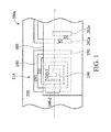
- FIG. 1 is a top view showing one exemplary embodiment of a semiconductor package 500a, especially showing a base with a radio-frequency (RF) device embedded therein for a semiconductor package.
- the semiconductor package can be a flip chip package using conductive structures, for example, copper pillar bumps, connecting a semiconductor device to a base.
- the semiconductor package can be a package using wire bonding technology to connect a semiconductor device to a base.
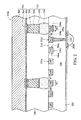
- FIG. 2 shows a partial cross section taken along a line A-A' of FIG. 1 , showing one exemplary embodiment of a semiconductor package 500a of the invention. Please refer to FIGS.
- the semiconductor package 500a comprises a base 200 having a device-attach surface 214 and a solder-ball-attach surface 213 opposite to the device-attach surface 214.
- the base 200 for example, a printed circuit board (PCB), may be formed of polypropylene (PP). It should also be noted that the base 200 can be a single layer or a multilayer structure.
- a radio-frequency (RF) device 240 is formed embedded in the base 200, close to the device-attach surface 214.
- the RF device 240 may comprise an inductor, antenna, filter, power amplifiers (PAs), decoupling or matching circuits.
- the RF device 240 is an inductor 240.
- the RF device 240 has two terminal portions 248 and 250 serving as pad regions 248 and 250 to connect to a semiconductor device 300 mounted directly onto the base 200.
- the RF device 240 has a plurality of device portions, for example, device portions 240-1 and 240-2.
- the device portions 240-1 and 240-2 of the RF device 240 may be designed to have a width W1 which is larger than 5 ⁇ m, and a minimum spacing S1 which is about 10-12 ⁇ m.
- W1 width W1 which is larger than 5 ⁇ m
- S1 minimum spacing S1
- first conductive traces 202a may also be designed to be embedded in the base 200, close to the device-attach surface 214.
- the first conductive traces 202a may comprise signal trace segments or ground trace segments, which are used for input/output (I/O) connections of the semiconductor device 300 mounted directly onto the base 200. Therefore, each of the first conductive traces 202a has a portion serving as a pad region of the base 200.
- the first conductive traces 202a are designed to have a width W2 which is larger than 5 ⁇ m, and a minimum spacing S2 which is about 10-12 ⁇ m.
- W2 width
- S2 minimum spacing
- a second conductive trace 202b may also be designed to be disposed on the solder-ball-attach surface 213 of the base 200.
- a solder-ball structure 252 may also be designed to be disposed on the second conductive trace 202b.
- a semiconductor device 300 is mounted on the device-attach surface 214 of the base 200 with an active surface of the semiconductor device 300 facing the base 200 by a bonding process.
- the semiconductor device 300 may comprise a die, a package, or a wafer-level package.
- the semiconductor device 300 is a flip chip package.
- the semiconductor device 300 may include a body 301, metal pads 304 overlying the semiconductor body 301, and an insulation layer 302 covering the metal pads 304.
- the circuitry of the semiconductor device 300 is disposed on the active surface, and the metal pads 304 are disposed on the top of the circuitry.
- the circuitry of the semiconductor device 300 is interconnected to the RF device 240 and the first conductive traces 202a embedded in the base 200 via a plurality of conductive structures 222 disposed on the active surface of the semiconductor device 300.
- the conductive structures 222 shown in FIG.2 are only an example and is not a limitation to the present invention.
- the conductive structure 222 may comprise a conductive bump structure such as a copper bump or a solder bump structure, a conductive wire structure, or a conductive paste structure.
- the conductive structure 222 may be a copper bump structure composed of a metal stack comprising a UBM (under-bump metallurgy) layer 306, a copper layer 216 such as a plated copper layer, a conductive buffer layer 218, and a solder cap 220.
- the UBM layer 306 can be formed on the exposed metal pads 304 within the openings by a deposition method such as a sputtering or plating method and a subsequent anisotropic etching process.
- the anisotropic etching process is performed after forming conductive pillars.
- the UBM layer 306 may also extend onto a top surface of the insulation layer 302.
- the UBM layer 306 may comprise titanium, copper, or a combination thereof
- a copper layer 216 such as an electroplated copper layer can be formed on the UBM layer 306.
- the opening can be filled with the copper layer 216 and the UBM layer 306, and the copper layer 216 and the UBM layer 306 within the opening may form an integral plug of the conductive structure 222.
- the formation position of the copper layer 216 is defined by a dry film photoresist or liquid photoresist patterns (not shown).
- an underfill material or the underfill 230 can be introduced into the gap between the semiconductor device 300 and the base 200.
- the underfill 230 may comprise a capillary underfill (CUF), molded underfill (MUF), or a combination thereof.
- the RF device 240 and the first conductive traces 202a may have a top surface disposed above, below, or aligned to a surface of the base to improve routing ability for high-density semiconductor packages.
- the RF device 240 has a top surface 242a disposed aligned to the device-attach surface 214 of the base 200. That is to say, the bottom surface 246a and at least a sidewall 244a of the RF device 240 are designed to be fully connected to the base 200.
- the first conductive traces 202a may have a similar arrangement to the RF device 240.
- the first conductive traces 202a have top surfaces 212a disposed aligned to the device-attach surface 214 of the base 200.
- the bottom surface 206a and a sidewall 204a of the conductive trace 202a are designed to be fully connected to the base 200.
- the solder cap 220 of the conductive structure 222 is disposed to contact with a portion of the base 200 and to connect to a top surface 242a of the RF device 240 and a top surface 212a of the first conductive trace 202a. Due to the top surfaces of the RF device and the first conductive traces being coplanar to the device-attach surface 214 of the base 200, the bump-to-trace space is increased and the problem of bump-to-trace bridging can be effectively avoided.
- FIG. 3 shows a partial cross section taken showing another exemplary embodiment of a semiconductor package 500b of the invention, especially showing a base 200a with a radio-frequency (RF) device embedded therein for a semiconductor package.
- the base 200a may comprise a multilayer structure.
- the multilayered base 200a may have a base portion 201 allowing the RF device 240 to be embedded therein.
- the multilayered base 200a further comprises an insulation layer 208 having openings therethrough disposed on the base portion 204 close to a device-attach surface 214 of the base portion 204.
- the base portion 201 and the insulation layer 208 collectively serve as a multilayer base 200a.
- the RF device 240 and the first conductive traces 202a embedded in the base portion 201 may be aligned to the device-attach surface 214 of the base portion 204.
- the RF device 240 and the first conductive traces 202a embedded in the base portion 201 may be exposed within the openings of the insulation layer 208.
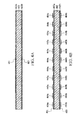
- FIGS. 4A to 4E are cross sections showing one exemplary embodiment of a method for fabricating two bases 200c and 200d with the RF devices for a semiconductor package of the invention.
- the method for fabricating bases for a semiconductor package is also called a double-sided base fabricating process.
- Elements of the embodiments that are the same or similar as those previously described with reference to FIGS. 1-3 are hereinafter not repeated for brevity.
- a carrier 400 with conductive seed layers 402a and 402b on the top surface 401 and the bottom surface 403 is provided.
- the carrier 400 may comprise FR4 glass epoxy or stainless steel.
- the conductive seed layers 402a and 402b are used as seed layers for subsequently formed interconnection conductive traces of bases on the top surface 401 and the bottom surface 403 of the carrier 400.
- the conductive seed layers 402a and 402b may comprise copper.
- RF devices 440a, 440b and first conductive traces 404a, 404b are formed simultaneously on the top surface 401 and the bottom surface 403 of the carrier 400. Bottom portions of the RF devices 440a, 440b and the first conductive traces 404a and 404b connect to top portions of the conductive seed layers 402a and 402b.
- the RF devices 440a, 440b and the first conductive traces 404a, 404b may be formed by a plating process and an anisotropic etching process. The plating process and the anisotropic etching process are performed simultaneously on the top surface 401 and the bottom surface 403 of the carrier 400.
- the plating process may comprise an electrical plating process.
- the RF devices 440a, 440b and the first conductive traces 404a, 404b may comprise copper (Cu).
- the RF devices 440a, 440b may serve as inductors 440a, 440b.
- the width W1 and the minimum spacing S1 of the RF devices 440a, 440b or the width W2 and the minimum spacing S2 of the first conductive traces 404a, 404b can be precisely controlled due to the formation processes, for example, the anisotropic etching process.
- the RF devices 440a, 440b may be designed to have a width W1 which is larger than 5 ⁇ m, and a minimum spacing S1 which is about 10-12 ⁇ m.
- the first conductive traces 404a, 404b may be designed to have a width W2 which is larger than 5 ⁇ m, and a minimum spacing S2 which is about 10-12 ⁇ m.
- the width S1 and S2 can be smaller than 5 ⁇ m if required.
- turns of the resulted inductor 440a, 440b embedded in the base can be increased over that of the conventional on-wafer inductor.
- the resulted inductor 440a, 440b has a dramatically increase in thickness compared to the conventional on-wafer inductor due to the formation processes, for example, the plating process.
- the inductor 440a, 440b is formed of copper (Cu), and the resistance of the inductor can be reduced from that of the conventional on-wafer inductor formed of aluminum (Al).
- a laminating process is performed to dispose a first base material layer 406a and a second base material layer 406b on the top surface 401 and the bottom surface 403 of the carrier 400, respectively, wherein the first base material layer 406a and a second base material layer 406b cover the RF devices 440a, 440b and the first conductive traces 404a and 404b, respectively.
- the laminating process of the first base material layer 406a and the second base material layer 406b is performed simultaneously on the on the top surface 401 and the bottom surface 403 of the carrier 400.
- the first base material layer 406a and the second base material layer 406b may comprise polypropylene (PP).
- a drilling process is performed to form openings (not shown) through the first base material layer 406a and the second base material layer 406b to define the formation positions of subsequently formed vias 408a, 408b, 448a and 448b.
- the drilling process may comprise a laser drilling process, an etching drilling process, or a mechanical drilling process.
- a plating process is performed to fill a conductive material into the openings to form vias 448a and 448b for interconnecting the RF devices 440a, 440b to subsequent second conductive traces 450a and 450b.
- the plating process is performed simultaneously to fill a conductive material into the openings to form vias 408a and 408b for interconnecting the first conductive traces 404a and 404b to subsequent second conductive traces 410a and 410b.
- the drilling process and the plating process are performed simultaneously on the first base material layer 406a and the second base material layer 406b, respectively.
- FIG. 4C wherein a plurality of second conductive traces 410a, 410b, 450a and 450b are respectively formed on a first surface 412 of the first base material layer 406a and a first surface 414 of the second base material layer 406b.
- the first surface 412 of the first base material layer 406a and the first surface 414 of the second base material layer 406b are away from the top surface 401 and the bottom surface 403 of the carrier 400, respectively.
- the second conductive traces 410a, 410b, 450a and 450b are formed by a plating process and an anisotropic etching process.
- the plating process and the anisotropic etching process are performed simultaneously on the first surface 412 of the first base material layer 406a and the first surface 414 of the second base material layer 406b.
- the plating process may comprise an electrical plating process.
- the second conductive traces 410a, 410b, 450a and 450b may comprise copper.
- the second conductive traces 410a, 410b, 450a and 450b are designed to have a width W2 which is larger than 5 ⁇ m, and a minimum spacing S2 which is about 10-12 ⁇ m. However, it should be noted that there is no limitation on the width of the conductive traces.
- the width of the second conductive traces 410a, 410b, 450a and 450b can be smaller than 5 ⁇ m if required.
- the anisotropic etching process may precisely control the width of the second conductive traces 410a, 410b, 450a and 450b.
- the first base material layer 406a which comprises the RF device 440a and the first conductive traces 404a embedded therein and second conductive traces 410a and 450a thereon
- the second base material layer 406b which comprises the RF device 440b and the first conductive traces 404b embedded therein and the second conductive traces 410b and 450b thereon
- the conductive seed layers 402a and 402b are removed from the first base 200c and the second base 200d, respectively.
- the RF device 440a, 440b and the first conductive traces 404a, 404b are aligned to second surfaces 416 and 418 of the of the first and second bases 200c and 200d, which are opposite to the first surfaces 412 and 414, respectively.
- the first base 200c and the second base 200d are fabricated simultaneously on opposite surfaces (the top surface 401 and the bottom surface 403) by the double-sided base fabricating process.
- a bonding process is performed to mount a semiconductor device (e.g. the semiconductor device 300 as shown in FIG. 2 ) on the first base 200c/second base 200d after the separation process through the conductive structure (e.g. the conductive structure 222 as shown in FIG. 2 ).
- the conductive structures are in contact with the top surface of the RF device 440a/440b and the first conductive traces 404a, 404b as shown in FIGS. 4D and 4E .
- an underfill material or the underfill e.g. the underfill 230 as shown in FIG. 2
- the first base 200c/second base 200d, the RF device 440a/440b, the conductive trace 404a/404b, the second conductive traces 410a/410b, 450a/450b as shown in FIGS. 4D and 4E , the semiconductor device (e.g. the semiconductor device 300 as shown in FIG. 2 ), and the conductive structure (e.g. the conductive structure 222 as shown in FIG. 2 ) may collectively form a semiconductor package (e.g. the semiconductor package 500a as shown in FIG. 2 ).
- two passivation or insulation layers e.g. the insulation layer 208 as shown in FIG. 3
- two passivation or insulation layers having openings may optionally be formed on the second surface 416 of the first base 200c and the second surface 418 of the second base 200d, respectively, after the separation of the first base 200c and the second base 200d as shown in FIGS. 4D and 4E .
- terminal portions of the RF device 440a, 440b, and the first conductive traces 404a and 404b of the first and second bases 200c and 200d are exposed within the opening.
- the first base 200c/second base 200d and the insulation layer thereon collectively serve as a multilayer base.
- the semiconductor device e.g. the semiconductor device 300 as shown in FIG. 2
- the conductive structure e.g. the conductive structure 222 as shown in FIG. 2
- the semiconductor package 500b may collectively form a semiconductor package.
- Exemplary embodiments provide a semiconductor package and a method for fabricating a base for a semiconductor package.
- the semiconductor package is designed to comprise RF devices, for example, inductors, embedded in a base such as a printed circuit board (PCB).
- the RF devices may have a top surface disposed above, below, or aligned to a surface of the base to improve routing ability for high-density semiconductor packages.
- the RF devices are designed to have a width which is larger than 5 ⁇ m, and a minimum spacing which is about 10-12 ⁇ m.
- the base may comprise a single layer structure or a multilayer structure. Exemplary embodiments also provide a method for fabricating a base for a semiconductor package.
- the method can fabricate two bases on two sides of a carrier simultaneously with the RF devices, for example, inductors, embedded in the base.
- the RF device may be formed by a plating process and an anisotropic etching process, and the anisotropic etching process may precisely control the width and minimum spacing of the RF device. Therefore, turns of the inductor embedded in the base can be increased over that of the conventional on-wafer inductor. Accordingly, the size of the semiconductor device (or die size) mounted on the base can be reduced, and the number of die-per-wafer can be increased.
- one exemplary embodiment of the inductor embedded in the base has a dramatically increase in thickness compared to that of the conventional on-wafer inductor due to the formation processes, for example, the plating process.
- one exemplary embodiment of the inductor embedded in a base is formed of copper (Cu), and the resistance of the inductor can be reduced from that of the conventional on-wafer inductor formed of aluminum (Al). Therefore, one exemplary embodiment of the inductor embedded in a base may have a higher quality factor (Q-factor) than the conventional on-wafer inductor.
- the method can fabricate a base comprising a single layer structure or a multilayer structure to improve design capability.
Landscapes
- Engineering & Computer Science (AREA)
- Microelectronics & Electronic Packaging (AREA)
- Manufacturing & Machinery (AREA)
- Power Engineering (AREA)
- Physics & Mathematics (AREA)
- Optics & Photonics (AREA)
- Internal Circuitry In Semiconductor Integrated Circuit Devices (AREA)
- Wire Bonding (AREA)
- Structures Or Materials For Encapsulating Or Coating Semiconductor Devices Or Solid State Devices (AREA)
- Semiconductor Integrated Circuits (AREA)
- Die Bonding (AREA)
- Production Of Multi-Layered Print Wiring Board (AREA)
Abstract
Description
- The present invention relates to a semiconductor package and a method for fabricating a base for a semiconductor package, and in particular, to a base with a radio-frequency (RF) device embedded therein for a semiconductor package.
- In high-speed applications (e.g. radio-frequency (RF) applications), the conventional RF device comprises several discrete RF chips and other active or passive devices (such as inductors, antennas, filters, power amplifiers (PAs), decoupling or matching circuits) mounted on an RF main die. However, the on-wafer inductors of the conventional RF device are formed of aluminum (Al), and the thickness of the on-wafer inductors is limited by the fabrication processes of the conventional RF device. Therefore, inductors of the conventional RF device, also referred to as on-wafer inductors, suffer from large area consumption and a low quality factor (Q-factor). Also, the size of the RF main die and the number of die-per-wafer of the conventional RF device cannot be reduced.
- Thus, a novel RF device package is desirable.
- A semiconductor package and a method for fabricating a base for a semiconductor package are provided. An exemplary embodiment of a semiconductor package includes a base having a device-attach surface. A radio-frequency (RF) device is embedded in the base, close to the device-attach surface.
- Another exemplary embodiment of a semiconductor package includes a radio-frequency (RF) device, having a bottom surface and a sidewall connected to a base. A semiconductor device is mounted on the RF device via a conductive structure.
- An exemplary embodiment of a method for fabricating a base for a semiconductor package includes providing a carrier with conductive seed layers on the top surface and the bottom surface of the carrier. Radio-frequency (RF) devices are respectively formed on the conductive seed layers. A first base material layer and a second base material layer are respectively laminated on the conductive seed layers, covering the RF devices. The first base material layer and the second base material layer, which contain the RF devices thereon, are separated from the carrier to form a first base and a second base.
- Another exemplary embodiment of a method for fabricating a semiconductor package includes providing a base. At least one radio-frequency (RF) device is formed on the base. An additional insulation material is formed on the base, and further defining patterns upon the additional insulation material, wherein the pattern is formed on the RF device(s).
- A detailed description is given in the following embodiments with reference to the accompanying drawings.
- The invention can be more fully understood by reading the subsequent detailed description and examples with references made to the accompanying drawings, wherein:
-
FIG. 1 is a top view showing one exemplary embodiment of a semiconductor package, especially showing a base with a radio-frequency (RF) device embedded therein for a semiconductor package. -
FIG. 2 is a partial cross section taken along a line A-A' ofFIG. 1 , showing one exemplary embodiment of a semiconductor package, especially showing a base with a radio-frequency (RF) device embedded therein for a semiconductor package. -
FIG. 3 shows a partial cross section taken showing another exemplary embodiment of a semiconductor package of the invention, especially showing a base with a radio-frequency (RF) device embedded therein for a semiconductor package. -
FIGS. 4A to 4E are cross sections showing one exemplary embodiment of a method for fabricating a base with an RF device for a semiconductor package of the invention. - The following description is a mode for carrying out the invention. This description is made for the purpose of illustrating the general principles of the invention and should not be taken in a limiting sense. The scope of the invention is best determined by reference to the appended claims. Wherever possible, the same reference numbers are used in the drawings and the descriptions to refer the same or like parts.
- The present invention will be described with respect to particular embodiments and with reference to certain drawings, but the invention is not limited thereto and is only limited by the claims. The drawings described are only schematic and are non-limiting. In the drawings, the size of some of the elements may be exaggerated and not drawn to scale for illustrative purposes. The dimensions and the relative dimensions do not correspond to actual dimensions to practice of the invention.
-
FIG. 1 is a top view showing one exemplary embodiment of asemiconductor package 500a, especially showing a base with a radio-frequency (RF) device embedded therein for a semiconductor package. In this embodiment, the semiconductor package can be a flip chip package using conductive structures, for example, copper pillar bumps, connecting a semiconductor device to a base. Alternatively, the semiconductor package can be a package using wire bonding technology to connect a semiconductor device to a base.FIG. 2 shows a partial cross section taken along a line A-A' ofFIG. 1 , showing one exemplary embodiment of asemiconductor package 500a of the invention. Please refer toFIGS. 1 and2 , wherein thesemiconductor package 500a comprises abase 200 having a device-attach surface 214 and a solder-ball-attach surface 213 opposite to the device-attach surface 214. In one embodiment, thebase 200, for example, a printed circuit board (PCB), may be formed of polypropylene (PP). It should also be noted that thebase 200 can be a single layer or a multilayer structure. In this embodiment, a radio-frequency (RF)device 240 is formed embedded in thebase 200, close to the device-attach surface 214. In one embodiment, theRF device 240 may comprise an inductor, antenna, filter, power amplifiers (PAs), decoupling or matching circuits. In this embodiment, theRF device 240 is aninductor 240. In this embodiment, theRF device 240 has twoterminal portions pad regions semiconductor device 300 mounted directly onto thebase 200. In this embodiment, theRF device 240 has a plurality of device portions, for example, device portions 240-1 and 240-2. The device portions 240-1 and 240-2 of theRF device 240 may be designed to have a width W1 which is larger than 5µm, and a minimum spacing S1 which is about 10-12µm. However, it should be noted that there is no limitation on the width W1 and the minimum spacing S1 of the device portions 240-1 and 240-2 of theRF device 240. - Alternatively, a plurality of first
conductive traces 202a may also be designed to be embedded in thebase 200, close to the device-attach surface 214. In one embodiment, the firstconductive traces 202a may comprise signal trace segments or ground trace segments, which are used for input/output (I/O) connections of thesemiconductor device 300 mounted directly onto thebase 200. Therefore, each of the firstconductive traces 202a has a portion serving as a pad region of thebase 200. In this embodiment, the firstconductive traces 202a are designed to have a width W2 which is larger than 5µm, and a minimum spacing S2 which is about 10-12µm. However, it should be noted that there is no limitation on the width of the conductive traces. For different designs, the width of the conductive traces can be smaller than 5µm if required. - In one embodiment as shown in
FIG. 2 , a secondconductive trace 202b may also be designed to be disposed on the solder-ball-attach surface 213 of thebase 200. In this embodiment, a solder-ball structure 252 may also be designed to be disposed on the secondconductive trace 202b. - A
semiconductor device 300 is mounted on the device-attach surface 214 of thebase 200 with an active surface of thesemiconductor device 300 facing thebase 200 by a bonding process. In one embodiment, thesemiconductor device 300 may comprise a die, a package, or a wafer-level package. In this embodiment, thesemiconductor device 300 is a flip chip package. As shown inFIG. 2 , thesemiconductor device 300 may include abody 301,metal pads 304 overlying thesemiconductor body 301, and aninsulation layer 302 covering themetal pads 304. The circuitry of thesemiconductor device 300 is disposed on the active surface, and themetal pads 304 are disposed on the top of the circuitry. The circuitry of thesemiconductor device 300 is interconnected to theRF device 240 and the firstconductive traces 202a embedded in thebase 200 via a plurality ofconductive structures 222 disposed on the active surface of thesemiconductor device 300. However, it should be noted that theconductive structures 222 shown inFIG.2 are only an example and is not a limitation to the present invention. - As shown in
FIG. 2 , theconductive structure 222 may comprise a conductive bump structure such as a copper bump or a solder bump structure, a conductive wire structure, or a conductive paste structure. In this embodiment, theconductive structure 222 may be a copper bump structure composed of a metal stack comprising a UBM (under-bump metallurgy)layer 306, acopper layer 216 such as a plated copper layer, aconductive buffer layer 218, and asolder cap 220. In one embodiment, theUBM layer 306 can be formed on the exposedmetal pads 304 within the openings by a deposition method such as a sputtering or plating method and a subsequent anisotropic etching process. The anisotropic etching process is performed after forming conductive pillars. TheUBM layer 306 may also extend onto a top surface of theinsulation layer 302. In this embodiment, theUBM layer 306 may comprise titanium, copper, or a combination thereof Acopper layer 216 such as an electroplated copper layer can be formed on theUBM layer 306. The opening can be filled with thecopper layer 216 and theUBM layer 306, and thecopper layer 216 and theUBM layer 306 within the opening may form an integral plug of theconductive structure 222. The formation position of thecopper layer 216 is defined by a dry film photoresist or liquid photoresist patterns (not shown). - In one embodiment, an underfill material or the
underfill 230 can be introduced into the gap between thesemiconductor device 300 and thebase 200. In one embodiment, theunderfill 230 may comprise a capillary underfill (CUF), molded underfill (MUF), or a combination thereof. - In one embodiment, the
RF device 240 and the firstconductive traces 202a may have a top surface disposed above, below, or aligned to a surface of the base to improve routing ability for high-density semiconductor packages. As shown inFIG. 2 , theRF device 240 has atop surface 242a disposed aligned to the device-attachsurface 214 of thebase 200. That is to say, thebottom surface 246a and at least asidewall 244a of theRF device 240 are designed to be fully connected to thebase 200. Alternatively, the firstconductive traces 202a may have a similar arrangement to theRF device 240. For example, the firstconductive traces 202a havetop surfaces 212a disposed aligned to the device-attachsurface 214 of thebase 200. Also, thebottom surface 206a and asidewall 204a of theconductive trace 202a are designed to be fully connected to thebase 200. In this embodiment, thesolder cap 220 of theconductive structure 222 is disposed to contact with a portion of thebase 200 and to connect to atop surface 242a of theRF device 240 and atop surface 212a of the firstconductive trace 202a. Due to the top surfaces of the RF device and the first conductive traces being coplanar to the device-attachsurface 214 of thebase 200, the bump-to-trace space is increased and the problem of bump-to-trace bridging can be effectively avoided. -
FIG. 3 shows a partial cross section taken showing another exemplary embodiment of asemiconductor package 500b of the invention, especially showing abase 200a with a radio-frequency (RF) device embedded therein for a semiconductor package. Alternatively, thebase 200a may comprise a multilayer structure. In this embodiment, themultilayered base 200a may have abase portion 201 allowing theRF device 240 to be embedded therein. Also, themultilayered base 200a further comprises aninsulation layer 208 having openings therethrough disposed on the base portion 204 close to a device-attachsurface 214 of the base portion 204. In this embodiment, thebase portion 201 and theinsulation layer 208 collectively serve as amultilayer base 200a. In this embodiment, theRF device 240 and the firstconductive traces 202a embedded in thebase portion 201. Thetop surface 242a of theRF device 240 and thetop surface 202a of the firstconductive traces 202a may be aligned to the device-attachsurface 214 of the base portion 204. In this embodiment, theRF device 240 and the firstconductive traces 202a embedded in thebase portion 201 may be exposed within the openings of theinsulation layer 208. -
FIGS. 4A to 4E are cross sections showing one exemplary embodiment of a method for fabricating twobases FIGS. 1-3 , are hereinafter not repeated for brevity. As shown inFIG. 4A , acarrier 400 withconductive seed layers top surface 401 and thebottom surface 403 is provided. In one embodiment, thecarrier 400 may comprise FR4 glass epoxy or stainless steel. Also, theconductive seed layers top surface 401 and thebottom surface 403 of thecarrier 400. In one embodiment, theconductive seed layers - Next, as shown in
FIG. 4B ,RF devices conductive traces top surface 401 and thebottom surface 403 of thecarrier 400. Bottom portions of theRF devices conductive traces conductive seed layers RF devices conductive traces top surface 401 and thebottom surface 403 of thecarrier 400. In one embodiment, the plating process may comprise an electrical plating process. In one embodiment, theRF devices conductive traces RF devices inductors RF devices conductive traces RF devices conductive traces inductor inductor inductor - Next, as shown in
FIG. 4C , a laminating process is performed to dispose a firstbase material layer 406a and a secondbase material layer 406b on thetop surface 401 and thebottom surface 403 of thecarrier 400, respectively, wherein the firstbase material layer 406a and a secondbase material layer 406b cover theRF devices conductive traces base material layer 406a and the secondbase material layer 406b is performed simultaneously on the on thetop surface 401 and thebottom surface 403 of thecarrier 400. In one embodiment, the firstbase material layer 406a and the secondbase material layer 406b may comprise polypropylene (PP). - Next, please refer to
FIG. 4C again, wherein a drilling process is performed to form openings (not shown) through the firstbase material layer 406a and the secondbase material layer 406b to define the formation positions of subsequently formed vias 408a, 408b, 448a and 448b. In one embodiment, the drilling process may comprise a laser drilling process, an etching drilling process, or a mechanical drilling process. Next, a plating process is performed to fill a conductive material into the openings to form vias 448a and 448b for interconnecting theRF devices conductive traces conductive traces conductive traces base material layer 406a and the secondbase material layer 406b, respectively. - Next, please refer to
FIG. 4C again, wherein a plurality of secondconductive traces first surface 412 of the firstbase material layer 406a and afirst surface 414 of the secondbase material layer 406b. As shown inFIG. 4C , thefirst surface 412 of the firstbase material layer 406a and thefirst surface 414 of the secondbase material layer 406b are away from thetop surface 401 and thebottom surface 403 of thecarrier 400, respectively. The secondconductive traces first surface 412 of the firstbase material layer 406a and thefirst surface 414 of the secondbase material layer 406b. In one embodiment, the plating process may comprise an electrical plating process. In one embodiment, the secondconductive traces conductive traces conductive traces conductive traces - Next, as shown in
FIGS. 4D and 4E , the firstbase material layer 406a, which comprises theRF device 440a and the firstconductive traces 404a embedded therein and secondconductive traces base material layer 406b, which comprises theRF device 440b and the firstconductive traces 404b embedded therein and the second conductive traces 410b and 450b thereon, are respectively separated from thetop surface 401 and thebottom surface 403 of thecarrier 400 to form afirst base 200c and asecond base 200d which are separated from each other. Next, as shown inFIGS. 4d and 4e again, theconductive seed layers first base 200c and thesecond base 200d, respectively. - As shown in
FIGS. 4D and 4E , theRF device conductive traces second surfaces second bases first surfaces first base 200c and thesecond base 200d are fabricated simultaneously on opposite surfaces (thetop surface 401 and the bottom surface 403) by the double-sided base fabricating process. - Next, a bonding process is performed to mount a semiconductor device (e.g. the
semiconductor device 300 as shown inFIG. 2 ) on thefirst base 200c/second base 200d after the separation process through the conductive structure (e.g. theconductive structure 222 as shown inFIG. 2 ). After the bonding process, the conductive structures are in contact with the top surface of theRF device 440a/440b and the firstconductive traces FIGS. 4D and 4E . Next, an underfill material or the underfill (e.g. theunderfill 230 as shown inFIG. 2 ) can be introduced into the gap between the semiconductor device and thefirst base 200c/second base 200d. Finally, thefirst base 200c/second base 200d, theRF device 440a/440b, theconductive trace 404a/404b, the secondconductive traces 410a/410b, 450a/450b as shown inFIGS. 4D and 4E , the semiconductor device (e.g. thesemiconductor device 300 as shown inFIG. 2 ), and the conductive structure (e.g. theconductive structure 222 as shown inFIG. 2 ) may collectively form a semiconductor package (e.g. thesemiconductor package 500a as shown inFIG. 2 ). - Alternatively, two passivation or insulation layers (e.g. the
insulation layer 208 as shown inFIG. 3 ) having openings may optionally be formed on thesecond surface 416 of thefirst base 200c and thesecond surface 418 of thesecond base 200d, respectively, after the separation of thefirst base 200c and thesecond base 200d as shown inFIGS. 4D and 4E . In this embodiment, terminal portions of theRF device conductive traces second bases first base 200c/second base 200d and the insulation layer thereon collectively serve as a multilayer base. After performing the bonding process and the underfill material/underfill introducing process, thefirst base 200c/second base 200d, theRF device 440a/440b, theconductive trace 404a/404b, the secondconductive traces 410a/410b, 450a/450b as shown inFIGS. 4D and 4E , the semiconductor device (e.g. thesemiconductor device 300 as shown inFIG. 2 ), and the conductive structure (e.g. theconductive structure 222 as shown inFIG. 2 ) may collectively form a semiconductor package (e.g. thesemiconductor package 500b as shown inFIG. 3 ). - Exemplary embodiments provide a semiconductor package and a method for fabricating a base for a semiconductor package. The semiconductor package is designed to comprise RF devices, for example, inductors, embedded in a base such as a printed circuit board (PCB). The RF devices may have a top surface disposed above, below, or aligned to a surface of the base to improve routing ability for high-density semiconductor packages. Also, the RF devices are designed to have a width which is larger than 5µm, and a minimum spacing which is about 10-12µm. Further, the base may comprise a single layer structure or a multilayer structure. Exemplary embodiments also provide a method for fabricating a base for a semiconductor package. In one embodiment, the method can fabricate two bases on two sides of a carrier simultaneously with the RF devices, for example, inductors, embedded in the base. Further, the RF device may be formed by a plating process and an anisotropic etching process, and the anisotropic etching process may precisely control the width and minimum spacing of the RF device. Therefore, turns of the inductor embedded in the base can be increased over that of the conventional on-wafer inductor. Accordingly, the size of the semiconductor device (or die size) mounted on the base can be reduced, and the number of die-per-wafer can be increased. Also, one exemplary embodiment of the inductor embedded in the base has a dramatically increase in thickness compared to that of the conventional on-wafer inductor due to the formation processes, for example, the plating process. Further, one exemplary embodiment of the inductor embedded in a base is formed of copper (Cu), and the resistance of the inductor can be reduced from that of the conventional on-wafer inductor formed of aluminum (Al). Therefore, one exemplary embodiment of the inductor embedded in a base may have a higher quality factor (Q-factor) than the conventional on-wafer inductor. Alternatively, the method can fabricate a base comprising a single layer structure or a multilayer structure to improve design capability.
- While the invention has been described by way of example and in terms of the preferred embodiments, it is to be understood that the invention is not limited to the disclosed embodiments. On the contrary, it is intended to cover various modifications and similar arrangements (as would be apparent to those skilled in the art). Therefore, the scope of the appended claims should be accorded the -broadest interpretation so as to encompass all such modifications and similar arrangements.
Claims (15)
- A semiconductor package (500a, 500b), comprising:a base (200, 200a) having a device-attach surface (214); anda radio-frequency (RF) device (240) embedded in the base, close to the device-attach surface.
- The semiconductor package as claimed in claim 1, further comprising:a first conductive trace (202a) embedded in the base, close to the device-attach surface (214); anda semiconductor device (300) mounted on the first conductive trace (202a) via a first conductive structure (222).
- The semiconductor package as claimed in claim 2, further comprising:a second conductive trace (202b) disposed on a solder-ball-attach surface (213) of the base, wherein the solder-ball-attach surface is opposite to the device-attach surface; anda solder-ball structure (252) disposed on the second conductive trace.
- The semiconductor package as claimed in any of claims 1 to 3, wherein the RF devices (240) have a width (W1) larger than 5µm, and wherein the RF device has a plurality of device portions (240-1, 240-2), and wherein the adjacent device portions separated by a portion of the base have a minimum spacing (S1) which is about 10-12µm.
- The semiconductor package as claimed in any of claims 2 to 4, wherein the RF device (240) has a top surface (242a) above, below, or aligned to the surface of the base.
- The semiconductor package as claimed in any of claims 2 to 5, further comprising:an insulation layer (208) having an opening disposed on the device-attach surface of the base, above the top surfaces (242a) of the RF device (240), wherein portions of the RF device is exposed within the opening.
- A method for fabricating a base for a semiconductor package, comprising:providing a carrier (400) with conductive seed layers (402a, 402b) on the top surface (401) and the bottom surface (403) of the carrier;forming radio-frequency (RF) devices (440a, 440b) respectively on the conductive seed layers;laminating a first base material layer (406a) and a second base material layer (406b) respectively on the conductive seed layers, covering the RF devices; andseparating the first base material layer the second base material layer, which contain the RF devices thereon, from the carrier to form a first base (200c) and a second base (200d).
- The method for fabricating a base for a semiconductor package as claimed in claim 7, further comprising:forming first conductive traces (404a, 404b) on the conductive seed layers before laminating the first base material layer and the second base material layer respectively on the conductive seed layers; andforming second conductive traces (410a, 410b, 450a, 450b) respectively on first surfaces (412, 414) of the first base material layer (406a) and the second base material layer (406b), wherein the first surfaces of the first base material layer and the second base material layer are respectively away from the top surface and the bottom surface of the carrier before separating the first base material layer the second base material layer from the carrier.
- The method for fabricating a base for a semiconductor package as claimed in claim 8, further comprising:performing a drilling process to form openings through the first base material layer and the second base material layer; andperforming a plating process to fill a conductive material into the opening to form a via (408a, 408b, 448a, 448b) for interconnecting the RF devices or the first conductive traces to the second conductive traces, before forming the second conductive traces.
- The method for fabricating a base for a semiconductor package as claimed in claim 9, wherein the drilling process comprises a laser drilling process, an etching drilling process, or a mechanical drilling process, and the plating process comprises an electrical plating process.
- The method for fabricating a base for a semiconductor package as claimed in any of claims 8 to 10, wherein the RF devices, the first conductive traces, and the second conductive traces are formed by a plating process and an anisotropic etching process.
- The method for fabricating a base for a semiconductor package as claimed in any of claims 7 to 11, further comprising:removing conductive seed layers from the first base and the second base.
- The method for fabricating a base for a semiconductor package as claimed in any of claims 8 to 12, further comprising:forming insulation layers having openings respectively on the first and second bases, wherein portions of the RF devices and the first conductive traces of the first and second bases are exposed within the openings.
- The method for fabricating a base for a semiconductor package as claimed in any of claims 7 to 13, wherein the RF devices and the first conductive traces of the first and second bases are aligned to second surfaces (416, 418) of the first and second bases, and wherein the second surfaces are respectively opposite to the first surfaces of the first and second bases.
- The method for fabricating a base for a semiconductor package as claimed in any of claims 7 to 14, wherein each of the RF devices has a width (W1) larger than 5µm, and wherein each of the RF devices has a plurality of device portions, and wherein the adjacent device portions separated by a portion of the base have a minimum spacing (S1) which is about 10-12µm.
Applications Claiming Priority (1)
| Application Number | Priority Date | Filing Date | Title |
|---|---|---|---|
| US14/205,836 US9922844B2 (en) | 2014-03-12 | 2014-03-12 | Semiconductor package and method for fabricating base for semiconductor package |
Publications (3)
| Publication Number | Publication Date |
|---|---|
| EP2919265A2 true EP2919265A2 (en) | 2015-09-16 |
| EP2919265A3 EP2919265A3 (en) | 2015-09-23 |
| EP2919265B1 EP2919265B1 (en) | 2019-06-26 |
Family
ID=52473796
Family Applications (1)
| Application Number | Title | Priority Date | Filing Date |
|---|---|---|---|
| EP15155491.2A Active EP2919265B1 (en) | 2014-03-12 | 2015-02-18 | Semiconductor package and its manufacturing method |
Country Status (3)
| Country | Link |
|---|---|
| US (5) | US9922844B2 (en) |
| EP (1) | EP2919265B1 (en) |
| CN (1) | CN104916623B (en) |
Cited By (1)
| Publication number | Priority date | Publication date | Assignee | Title |
|---|---|---|---|---|
| KR20180052752A (en) * | 2015-10-08 | 2018-05-18 | 롬 앤드 하스 일렉트로닉 머트어리얼즈 엘엘씨 | Copper electroplating baths containing compounds of the reaction product of amine, polyacrylamide and sulphon |
Families Citing this family (8)
| Publication number | Priority date | Publication date | Assignee | Title |
|---|---|---|---|---|
| JP6432512B2 (en) * | 2013-08-14 | 2018-12-05 | 株式会社村田製作所 | Surface acoustic wave device, electronic component, and method of manufacturing surface acoustic wave device |
| US9922844B2 (en) * | 2014-03-12 | 2018-03-20 | Mediatek Inc. | Semiconductor package and method for fabricating base for semiconductor package |
| US10319689B2 (en) * | 2015-12-01 | 2019-06-11 | Nxp Usa, Inc. | Antenna assembly for wafer level packaging |
| CN105870026B (en) * | 2016-03-07 | 2019-03-19 | 武汉光谷创元电子有限公司 | Carrier, method for manufacturing the same, and method for manufacturing a coreless package substrate using the carrier |
| WO2017171884A1 (en) * | 2016-04-02 | 2017-10-05 | Intel Corporation | Fine feature formation techniques for printed circuit boards |
| MY192389A (en) | 2016-07-01 | 2022-08-18 | Intel Corp | Systems, methods, and apparatuses for implementing a pad on solder mask (posm) semiconductor substrate package |
| US10475718B2 (en) * | 2017-05-18 | 2019-11-12 | Advanced Semiconductor Engineering, Inc. | Semiconductor device package comprising a dielectric layer with built-in inductor |
| TWI697078B (en) * | 2018-08-03 | 2020-06-21 | 欣興電子股份有限公司 | Package substrate structure and method of bonding using the same |
Family Cites Families (10)
| Publication number | Priority date | Publication date | Assignee | Title |
|---|---|---|---|---|
| TWI260075B (en) * | 2005-10-24 | 2006-08-11 | Via Tech Inc | Embedded inductor element and chip package applying the same |
| US7519328B2 (en) * | 2006-01-19 | 2009-04-14 | Murata Manufacturing Co., Ltd. | Wireless IC device and component for wireless IC device |
| US8009101B2 (en) * | 2007-04-06 | 2011-08-30 | Murata Manufacturing Co., Ltd. | Wireless IC device |
| FI121909B (en) | 2008-04-18 | 2011-05-31 | Imbera Electronics Oy | Circuit boards and procedure for its manufacture |
| US7842542B2 (en) | 2008-07-14 | 2010-11-30 | Stats Chippac, Ltd. | Embedded semiconductor die package and method of making the same using metal frame carrier |
| US7642128B1 (en) * | 2008-12-12 | 2010-01-05 | Stats Chippac, Ltd. | Semiconductor device and method of forming a vertical interconnect structure for 3-D FO-WLCSP |
| US8163597B2 (en) | 2009-03-24 | 2012-04-24 | Stats Chippac, Ltd. | Semiconductor device and method of forming no-flow underfill material around vertical interconnect structure |
| US20110050334A1 (en) * | 2009-09-02 | 2011-03-03 | Qualcomm Incorporated | Integrated Voltage Regulator with Embedded Passive Device(s) |
| JP2014022551A (en) * | 2012-07-18 | 2014-02-03 | Ibiden Co Ltd | Printed wiring board and manufacturing method for printed wiring board |
| US9922844B2 (en) | 2014-03-12 | 2018-03-20 | Mediatek Inc. | Semiconductor package and method for fabricating base for semiconductor package |
-
2014
- 2014-03-12 US US14/205,836 patent/US9922844B2/en active Active
-
2015
- 2015-02-18 EP EP15155491.2A patent/EP2919265B1/en active Active
- 2015-03-12 CN CN201510108355.7A patent/CN104916623B/en active Active
- 2015-03-20 US US14/663,772 patent/US10115604B2/en active Active
-
2018
- 2018-02-09 US US15/893,527 patent/US10236187B2/en active Active
-
2019
- 2019-01-31 US US16/264,250 patent/US10573536B2/en active Active
-
2020
- 2020-01-15 US US16/743,866 patent/US10916449B2/en active Active
Non-Patent Citations (1)
| Title |
|---|
| None |
Cited By (1)
| Publication number | Priority date | Publication date | Assignee | Title |
|---|---|---|---|---|
| KR20180052752A (en) * | 2015-10-08 | 2018-05-18 | 롬 앤드 하스 일렉트로닉 머트어리얼즈 엘엘씨 | Copper electroplating baths containing compounds of the reaction product of amine, polyacrylamide and sulphon |
Also Published As
| Publication number | Publication date |
|---|---|
| US9922844B2 (en) | 2018-03-20 |
| EP2919265A3 (en) | 2015-09-23 |
| US10236187B2 (en) | 2019-03-19 |
| US10573536B2 (en) | 2020-02-25 |
| US20150262840A1 (en) | 2015-09-17 |
| CN104916623B (en) | 2018-10-26 |
| US10916449B2 (en) | 2021-02-09 |
| CN104916623A (en) | 2015-09-16 |
| US10115604B2 (en) | 2018-10-30 |
| US20180166297A1 (en) | 2018-06-14 |
| US20200152479A1 (en) | 2020-05-14 |
| US20150264814A1 (en) | 2015-09-17 |
| EP2919265B1 (en) | 2019-06-26 |
| US20190164780A1 (en) | 2019-05-30 |
Similar Documents
| Publication | Publication Date | Title |
|---|---|---|
| EP2919265B1 (en) | Semiconductor package and its manufacturing method | |
| US11469201B2 (en) | Semiconductor package and method for fabricating base for semiconductor package | |
| US9177899B2 (en) | Semiconductor package and method for fabricating base for semiconductor package | |
| US20240332159A1 (en) | Semiconductor package and manufacturing method thereof | |
| US20230207416A1 (en) | Semiconductor packages | |
| US9232665B2 (en) | Method of fabricating packaging substrate having a passive element embedded therein | |
| US20200051954A1 (en) | Semiconductor package and method of fabricating the same | |
| US20140191397A1 (en) | Package substrate and semiconductor package including the same | |
| EP3120674B1 (en) | Face-up substrate integration with solder ball connection in semiconductor package | |
| US9627224B2 (en) | Semiconductor device with sloped sidewall and related methods | |
| CN107845614A (en) | A kind of integrated circuit module structure and preparation method thereof | |
| KR101432488B1 (en) | Stack type semiconductor package and methods for fabricating the same | |
| US20120025376A1 (en) | Ball grid array package |
Legal Events
| Date | Code | Title | Description |
|---|---|---|---|
| PUAL | Search report despatched |
Free format text: ORIGINAL CODE: 0009013 |
|
| PUAI | Public reference made under article 153(3) epc to a published international application that has entered the european phase |
Free format text: ORIGINAL CODE: 0009012 |
|
| AK | Designated contracting states |
Kind code of ref document: A2 Designated state(s): AL AT BE BG CH CY CZ DE DK EE ES FI FR GB GR HR HU IE IS IT LI LT LU LV MC MK MT NL NO PL PT RO RS SE SI SK SM TR |
|
| AX | Request for extension of the european patent |
Extension state: BA ME |
|
| AK | Designated contracting states |
Kind code of ref document: A3 Designated state(s): AL AT BE BG CH CY CZ DE DK EE ES FI FR GB GR HR HU IE IS IT LI LT LU LV MC MK MT NL NO PL PT RO RS SE SI SK SM TR |
|
| AX | Request for extension of the european patent |
Extension state: BA ME |
|
| RIC1 | Information provided on ipc code assigned before grant |
Ipc: H05K 3/28 20060101ALI20150820BHEP Ipc: H01L 23/538 20060101ALI20150820BHEP Ipc: H05K 1/02 20060101ALI20150820BHEP Ipc: H01L 23/64 20060101ALI20150820BHEP Ipc: H01L 25/00 20060101ALI20150820BHEP Ipc: H01L 23/66 20060101AFI20150820BHEP |
|
| 17P | Request for examination filed |
Effective date: 20160315 |
|
| RBV | Designated contracting states (corrected) |
Designated state(s): AL AT BE BG CH CY CZ DE DK EE ES FI FR GB GR HR HU IE IS IT LI LT LU LV MC MK MT NL NO PL PT RO RS SE SI SK SM TR |
|
| STAA | Information on the status of an ep patent application or granted ep patent |
Free format text: STATUS: EXAMINATION IS IN PROGRESS |
|
| 17Q | First examination report despatched |
Effective date: 20180515 |
|
| RIC1 | Information provided on ipc code assigned before grant |
Ipc: H01L 21/683 20060101ALI20181129BHEP Ipc: H01L 21/56 20060101ALI20181129BHEP Ipc: H01L 23/64 20060101ALI20181129BHEP Ipc: H01L 23/538 20060101ALI20181129BHEP Ipc: H01L 23/66 20060101AFI20181129BHEP Ipc: H01L 23/498 20060101ALI20181129BHEP Ipc: H01L 23/00 20060101ALI20181129BHEP Ipc: H05K 1/02 20060101ALI20181129BHEP Ipc: H01L 21/48 20060101ALI20181129BHEP Ipc: H05K 1/16 20060101ALI20181129BHEP Ipc: H01F 17/00 20060101ALI20181129BHEP Ipc: H01L 21/70 20060101ALI20181129BHEP Ipc: H01L 25/00 20060101ALI20181129BHEP Ipc: H05K 3/28 20060101ALI20181129BHEP |
|
| GRAP | Despatch of communication of intention to grant a patent |
Free format text: ORIGINAL CODE: EPIDOSNIGR1 |
|
| STAA | Information on the status of an ep patent application or granted ep patent |
Free format text: STATUS: GRANT OF PATENT IS INTENDED |
|
| INTG | Intention to grant announced |
Effective date: 20190107 |
|
| RIN1 | Information on inventor provided before grant (corrected) |
Inventor name: HSU, WEN-SUNG Inventor name: YU, TA-JEN |
|
| GRAJ | Information related to disapproval of communication of intention to grant by the applicant or resumption of examination proceedings by the epo deleted |
Free format text: ORIGINAL CODE: EPIDOSDIGR1 |
|
| STAA | Information on the status of an ep patent application or granted ep patent |
Free format text: STATUS: EXAMINATION IS IN PROGRESS |
|
| GRAR | Information related to intention to grant a patent recorded |
Free format text: ORIGINAL CODE: EPIDOSNIGR71 |
|
| GRAS | Grant fee paid |
Free format text: ORIGINAL CODE: EPIDOSNIGR3 |
|
| STAA | Information on the status of an ep patent application or granted ep patent |
Free format text: STATUS: GRANT OF PATENT IS INTENDED |
|
| GRAA | (expected) grant |
Free format text: ORIGINAL CODE: 0009210 |
|
| STAA | Information on the status of an ep patent application or granted ep patent |
Free format text: STATUS: THE PATENT HAS BEEN GRANTED |
|
| INTC | Intention to grant announced (deleted) | ||
| AK | Designated contracting states |
Kind code of ref document: B1 Designated state(s): AL AT BE BG CH CY CZ DE DK EE ES FI FR GB GR HR HU IE IS IT LI LT LU LV MC MK MT NL NO PL PT RO RS SE SI SK SM TR |
|
| INTG | Intention to grant announced |
Effective date: 20190520 |
|
| REG | Reference to a national code |
Ref country code: GB Ref legal event code: FG4D |
|
| REG | Reference to a national code |
Ref country code: CH Ref legal event code: EP |
|
| REG | Reference to a national code |
Ref country code: AT Ref legal event code: REF Ref document number: 1149295 Country of ref document: AT Kind code of ref document: T Effective date: 20190715 |
|
| REG | Reference to a national code |
Ref country code: DE Ref legal event code: R096 Ref document number: 602015032560 Country of ref document: DE |
|
| REG | Reference to a national code |
Ref country code: IE Ref legal event code: FG4D |
|
| REG | Reference to a national code |
Ref country code: NL Ref legal event code: MP Effective date: 20190626 |
|
| PG25 | Lapsed in a contracting state [announced via postgrant information from national office to epo] |
Ref country code: SE Free format text: LAPSE BECAUSE OF FAILURE TO SUBMIT A TRANSLATION OF THE DESCRIPTION OR TO PAY THE FEE WITHIN THE PRESCRIBED TIME-LIMIT Effective date: 20190626 Ref country code: AL Free format text: LAPSE BECAUSE OF FAILURE TO SUBMIT A TRANSLATION OF THE DESCRIPTION OR TO PAY THE FEE WITHIN THE PRESCRIBED TIME-LIMIT Effective date: 20190626 Ref country code: FI Free format text: LAPSE BECAUSE OF FAILURE TO SUBMIT A TRANSLATION OF THE DESCRIPTION OR TO PAY THE FEE WITHIN THE PRESCRIBED TIME-LIMIT Effective date: 20190626 Ref country code: NO Free format text: LAPSE BECAUSE OF FAILURE TO SUBMIT A TRANSLATION OF THE DESCRIPTION OR TO PAY THE FEE WITHIN THE PRESCRIBED TIME-LIMIT Effective date: 20190926 Ref country code: LT Free format text: LAPSE BECAUSE OF FAILURE TO SUBMIT A TRANSLATION OF THE DESCRIPTION OR TO PAY THE FEE WITHIN THE PRESCRIBED TIME-LIMIT Effective date: 20190626 Ref country code: HR Free format text: LAPSE BECAUSE OF FAILURE TO SUBMIT A TRANSLATION OF THE DESCRIPTION OR TO PAY THE FEE WITHIN THE PRESCRIBED TIME-LIMIT Effective date: 20190626 |
|
| REG | Reference to a national code |
Ref country code: LT Ref legal event code: MG4D |
|
| PG25 | Lapsed in a contracting state [announced via postgrant information from national office to epo] |
Ref country code: GR Free format text: LAPSE BECAUSE OF FAILURE TO SUBMIT A TRANSLATION OF THE DESCRIPTION OR TO PAY THE FEE WITHIN THE PRESCRIBED TIME-LIMIT Effective date: 20190927 Ref country code: BG Free format text: LAPSE BECAUSE OF FAILURE TO SUBMIT A TRANSLATION OF THE DESCRIPTION OR TO PAY THE FEE WITHIN THE PRESCRIBED TIME-LIMIT Effective date: 20190926 Ref country code: LV Free format text: LAPSE BECAUSE OF FAILURE TO SUBMIT A TRANSLATION OF THE DESCRIPTION OR TO PAY THE FEE WITHIN THE PRESCRIBED TIME-LIMIT Effective date: 20190626 Ref country code: RS Free format text: LAPSE BECAUSE OF FAILURE TO SUBMIT A TRANSLATION OF THE DESCRIPTION OR TO PAY THE FEE WITHIN THE PRESCRIBED TIME-LIMIT Effective date: 20190626 |
|
| REG | Reference to a national code |
Ref country code: AT Ref legal event code: MK05 Ref document number: 1149295 Country of ref document: AT Kind code of ref document: T Effective date: 20190626 |
|
| PG25 | Lapsed in a contracting state [announced via postgrant information from national office to epo] |
Ref country code: AT Free format text: LAPSE BECAUSE OF FAILURE TO SUBMIT A TRANSLATION OF THE DESCRIPTION OR TO PAY THE FEE WITHIN THE PRESCRIBED TIME-LIMIT Effective date: 20190626 Ref country code: PT Free format text: LAPSE BECAUSE OF FAILURE TO SUBMIT A TRANSLATION OF THE DESCRIPTION OR TO PAY THE FEE WITHIN THE PRESCRIBED TIME-LIMIT Effective date: 20191028 Ref country code: EE Free format text: LAPSE BECAUSE OF FAILURE TO SUBMIT A TRANSLATION OF THE DESCRIPTION OR TO PAY THE FEE WITHIN THE PRESCRIBED TIME-LIMIT Effective date: 20190626 Ref country code: CZ Free format text: LAPSE BECAUSE OF FAILURE TO SUBMIT A TRANSLATION OF THE DESCRIPTION OR TO PAY THE FEE WITHIN THE PRESCRIBED TIME-LIMIT Effective date: 20190626 Ref country code: NL Free format text: LAPSE BECAUSE OF FAILURE TO SUBMIT A TRANSLATION OF THE DESCRIPTION OR TO PAY THE FEE WITHIN THE PRESCRIBED TIME-LIMIT Effective date: 20190626 Ref country code: RO Free format text: LAPSE BECAUSE OF FAILURE TO SUBMIT A TRANSLATION OF THE DESCRIPTION OR TO PAY THE FEE WITHIN THE PRESCRIBED TIME-LIMIT Effective date: 20190626 Ref country code: SK Free format text: LAPSE BECAUSE OF FAILURE TO SUBMIT A TRANSLATION OF THE DESCRIPTION OR TO PAY THE FEE WITHIN THE PRESCRIBED TIME-LIMIT Effective date: 20190626 |
|
| PG25 | Lapsed in a contracting state [announced via postgrant information from national office to epo] |
Ref country code: ES Free format text: LAPSE BECAUSE OF FAILURE TO SUBMIT A TRANSLATION OF THE DESCRIPTION OR TO PAY THE FEE WITHIN THE PRESCRIBED TIME-LIMIT Effective date: 20190626 Ref country code: IT Free format text: LAPSE BECAUSE OF FAILURE TO SUBMIT A TRANSLATION OF THE DESCRIPTION OR TO PAY THE FEE WITHIN THE PRESCRIBED TIME-LIMIT Effective date: 20190626 Ref country code: IS Free format text: LAPSE BECAUSE OF FAILURE TO SUBMIT A TRANSLATION OF THE DESCRIPTION OR TO PAY THE FEE WITHIN THE PRESCRIBED TIME-LIMIT Effective date: 20191026 Ref country code: SM Free format text: LAPSE BECAUSE OF FAILURE TO SUBMIT A TRANSLATION OF THE DESCRIPTION OR TO PAY THE FEE WITHIN THE PRESCRIBED TIME-LIMIT Effective date: 20190626 |
|
| PG25 | Lapsed in a contracting state [announced via postgrant information from national office to epo] |
Ref country code: TR Free format text: LAPSE BECAUSE OF FAILURE TO SUBMIT A TRANSLATION OF THE DESCRIPTION OR TO PAY THE FEE WITHIN THE PRESCRIBED TIME-LIMIT Effective date: 20190626 |
|
| PG25 | Lapsed in a contracting state [announced via postgrant information from national office to epo] |
Ref country code: DK Free format text: LAPSE BECAUSE OF FAILURE TO SUBMIT A TRANSLATION OF THE DESCRIPTION OR TO PAY THE FEE WITHIN THE PRESCRIBED TIME-LIMIT Effective date: 20190626 Ref country code: PL Free format text: LAPSE BECAUSE OF FAILURE TO SUBMIT A TRANSLATION OF THE DESCRIPTION OR TO PAY THE FEE WITHIN THE PRESCRIBED TIME-LIMIT Effective date: 20190626 |
|
| PG25 | Lapsed in a contracting state [announced via postgrant information from national office to epo] |
Ref country code: IS Free format text: LAPSE BECAUSE OF FAILURE TO SUBMIT A TRANSLATION OF THE DESCRIPTION OR TO PAY THE FEE WITHIN THE PRESCRIBED TIME-LIMIT Effective date: 20200224 |
|
| REG | Reference to a national code |
Ref country code: DE Ref legal event code: R097 Ref document number: 602015032560 Country of ref document: DE |
|
| PLBE | No opposition filed within time limit |
Free format text: ORIGINAL CODE: 0009261 |
|
| STAA | Information on the status of an ep patent application or granted ep patent |
Free format text: STATUS: NO OPPOSITION FILED WITHIN TIME LIMIT |
|
| PG2D | Information on lapse in contracting state deleted |
Ref country code: IS |
|
| 26N | No opposition filed |
Effective date: 20200603 |
|
| PG25 | Lapsed in a contracting state [announced via postgrant information from national office to epo] |
Ref country code: SI Free format text: LAPSE BECAUSE OF FAILURE TO SUBMIT A TRANSLATION OF THE DESCRIPTION OR TO PAY THE FEE WITHIN THE PRESCRIBED TIME-LIMIT Effective date: 20190626 |
|
| REG | Reference to a national code |
Ref country code: CH Ref legal event code: PL |
|
| REG | Reference to a national code |
Ref country code: BE Ref legal event code: MM Effective date: 20200229 |
|
| PG25 | Lapsed in a contracting state [announced via postgrant information from national office to epo] |
Ref country code: LU Free format text: LAPSE BECAUSE OF NON-PAYMENT OF DUE FEES Effective date: 20200218 Ref country code: MC Free format text: LAPSE BECAUSE OF FAILURE TO SUBMIT A TRANSLATION OF THE DESCRIPTION OR TO PAY THE FEE WITHIN THE PRESCRIBED TIME-LIMIT Effective date: 20190626 |
|
| PG25 | Lapsed in a contracting state [announced via postgrant information from national office to epo] |
Ref country code: LI Free format text: LAPSE BECAUSE OF NON-PAYMENT OF DUE FEES Effective date: 20200229 Ref country code: CH Free format text: LAPSE BECAUSE OF NON-PAYMENT OF DUE FEES Effective date: 20200229 |
|
| PG25 | Lapsed in a contracting state [announced via postgrant information from national office to epo] |
Ref country code: IE Free format text: LAPSE BECAUSE OF NON-PAYMENT OF DUE FEES Effective date: 20200218 |
|
| PG25 | Lapsed in a contracting state [announced via postgrant information from national office to epo] |
Ref country code: BE Free format text: LAPSE BECAUSE OF NON-PAYMENT OF DUE FEES Effective date: 20200229 |
|
| PG25 | Lapsed in a contracting state [announced via postgrant information from national office to epo] |
Ref country code: MT Free format text: LAPSE BECAUSE OF FAILURE TO SUBMIT A TRANSLATION OF THE DESCRIPTION OR TO PAY THE FEE WITHIN THE PRESCRIBED TIME-LIMIT Effective date: 20190626 Ref country code: CY Free format text: LAPSE BECAUSE OF FAILURE TO SUBMIT A TRANSLATION OF THE DESCRIPTION OR TO PAY THE FEE WITHIN THE PRESCRIBED TIME-LIMIT Effective date: 20190626 |
|
| PG25 | Lapsed in a contracting state [announced via postgrant information from national office to epo] |
Ref country code: MK Free format text: LAPSE BECAUSE OF FAILURE TO SUBMIT A TRANSLATION OF THE DESCRIPTION OR TO PAY THE FEE WITHIN THE PRESCRIBED TIME-LIMIT Effective date: 20190626 |
|
| P01 | Opt-out of the competence of the unified patent court (upc) registered |
Effective date: 20230607 |
|
| REG | Reference to a national code |
Ref country code: DE Ref legal event code: R079 Ref document number: 602015032560 Country of ref document: DE Free format text: PREVIOUS MAIN CLASS: H01L0023660000 Ipc: H10W0044200000 |
|
| PGFP | Annual fee paid to national office [announced via postgrant information from national office to epo] |
Ref country code: FR Payment date: 20251208 Year of fee payment: 12 |
|
| PGFP | Annual fee paid to national office [announced via postgrant information from national office to epo] |
Ref country code: GB Payment date: 20260106 Year of fee payment: 12 |
|
| PGFP | Annual fee paid to national office [announced via postgrant information from national office to epo] |
Ref country code: DE Payment date: 20251224 Year of fee payment: 12 |