EP2918396A1 - Machine and method for additive manufacturing - Google Patents
Machine and method for additive manufacturing Download PDFInfo
- Publication number
- EP2918396A1 EP2918396A1 EP15158295.4A EP15158295A EP2918396A1 EP 2918396 A1 EP2918396 A1 EP 2918396A1 EP 15158295 A EP15158295 A EP 15158295A EP 2918396 A1 EP2918396 A1 EP 2918396A1
- Authority
- EP
- European Patent Office
- Prior art keywords
- electron beam
- powdered material
- pulsed
- additive manufacturing
- electron
- Prior art date
- Legal status (The legal status is an assumption and is not a legal conclusion. Google has not performed a legal analysis and makes no representation as to the accuracy of the status listed.)
- Withdrawn
Links
Images



Classifications
-
- B—PERFORMING OPERATIONS; TRANSPORTING
- B23—MACHINE TOOLS; METAL-WORKING NOT OTHERWISE PROVIDED FOR
- B23K—SOLDERING OR UNSOLDERING; WELDING; CLADDING OR PLATING BY SOLDERING OR WELDING; CUTTING BY APPLYING HEAT LOCALLY, e.g. FLAME CUTTING; WORKING BY LASER BEAM
- B23K15/00—Electron-beam welding or cutting
- B23K15/0026—Auxiliary equipment
-
- B—PERFORMING OPERATIONS; TRANSPORTING
- B22—CASTING; POWDER METALLURGY
- B22F—WORKING METALLIC POWDER; MANUFACTURE OF ARTICLES FROM METALLIC POWDER; MAKING METALLIC POWDER; APPARATUS OR DEVICES SPECIALLY ADAPTED FOR METALLIC POWDER
- B22F10/00—Additive manufacturing of workpieces or articles from metallic powder
- B22F10/20—Direct sintering or melting
- B22F10/28—Powder bed fusion, e.g. selective laser melting [SLM] or electron beam melting [EBM]
-
- B—PERFORMING OPERATIONS; TRANSPORTING
- B22—CASTING; POWDER METALLURGY
- B22F—WORKING METALLIC POWDER; MANUFACTURE OF ARTICLES FROM METALLIC POWDER; MAKING METALLIC POWDER; APPARATUS OR DEVICES SPECIALLY ADAPTED FOR METALLIC POWDER
- B22F10/00—Additive manufacturing of workpieces or articles from metallic powder
- B22F10/30—Process control
- B22F10/36—Process control of energy beam parameters
-
- B—PERFORMING OPERATIONS; TRANSPORTING
- B22—CASTING; POWDER METALLURGY
- B22F—WORKING METALLIC POWDER; MANUFACTURE OF ARTICLES FROM METALLIC POWDER; MAKING METALLIC POWDER; APPARATUS OR DEVICES SPECIALLY ADAPTED FOR METALLIC POWDER
- B22F12/00—Apparatus or devices specially adapted for additive manufacturing; Auxiliary means for additive manufacturing; Combinations of additive manufacturing apparatus or devices with other processing apparatus or devices
- B22F12/40—Radiation means
- B22F12/41—Radiation means characterised by the type, e.g. laser or electron beam
- B22F12/43—Radiation means characterised by the type, e.g. laser or electron beam pulsed; frequency modulated
-
- B—PERFORMING OPERATIONS; TRANSPORTING
- B22—CASTING; POWDER METALLURGY
- B22F—WORKING METALLIC POWDER; MANUFACTURE OF ARTICLES FROM METALLIC POWDER; MAKING METALLIC POWDER; APPARATUS OR DEVICES SPECIALLY ADAPTED FOR METALLIC POWDER
- B22F12/00—Apparatus or devices specially adapted for additive manufacturing; Auxiliary means for additive manufacturing; Combinations of additive manufacturing apparatus or devices with other processing apparatus or devices
- B22F12/40—Radiation means
- B22F12/44—Radiation means characterised by the configuration of the radiation means
-
- B—PERFORMING OPERATIONS; TRANSPORTING
- B22—CASTING; POWDER METALLURGY
- B22F—WORKING METALLIC POWDER; MANUFACTURE OF ARTICLES FROM METALLIC POWDER; MAKING METALLIC POWDER; APPARATUS OR DEVICES SPECIALLY ADAPTED FOR METALLIC POWDER
- B22F12/00—Apparatus or devices specially adapted for additive manufacturing; Auxiliary means for additive manufacturing; Combinations of additive manufacturing apparatus or devices with other processing apparatus or devices
- B22F12/40—Radiation means
- B22F12/49—Scanners
-
- B—PERFORMING OPERATIONS; TRANSPORTING
- B23—MACHINE TOOLS; METAL-WORKING NOT OTHERWISE PROVIDED FOR
- B23K—SOLDERING OR UNSOLDERING; WELDING; CLADDING OR PLATING BY SOLDERING OR WELDING; CUTTING BY APPLYING HEAT LOCALLY, e.g. FLAME CUTTING; WORKING BY LASER BEAM
- B23K15/00—Electron-beam welding or cutting
- B23K15/0046—Welding
- B23K15/0086—Welding welding for purposes other than joining, e.g. build-up welding
-
- B—PERFORMING OPERATIONS; TRANSPORTING
- B23—MACHINE TOOLS; METAL-WORKING NOT OTHERWISE PROVIDED FOR
- B23K—SOLDERING OR UNSOLDERING; WELDING; CLADDING OR PLATING BY SOLDERING OR WELDING; CUTTING BY APPLYING HEAT LOCALLY, e.g. FLAME CUTTING; WORKING BY LASER BEAM
- B23K15/00—Electron-beam welding or cutting
- B23K15/0046—Welding
- B23K15/0093—Welding characterised by the properties of the materials to be welded
-
- B—PERFORMING OPERATIONS; TRANSPORTING
- B23—MACHINE TOOLS; METAL-WORKING NOT OTHERWISE PROVIDED FOR
- B23K—SOLDERING OR UNSOLDERING; WELDING; CLADDING OR PLATING BY SOLDERING OR WELDING; CUTTING BY APPLYING HEAT LOCALLY, e.g. FLAME CUTTING; WORKING BY LASER BEAM
- B23K15/00—Electron-beam welding or cutting
- B23K15/02—Control circuits therefor
-
- B—PERFORMING OPERATIONS; TRANSPORTING
- B28—WORKING CEMENT, CLAY, OR STONE
- B28B—SHAPING CLAY OR OTHER CERAMIC COMPOSITIONS; SHAPING SLAG; SHAPING MIXTURES CONTAINING CEMENTITIOUS MATERIAL, e.g. PLASTER
- B28B1/00—Producing shaped prefabricated articles from the material
- B28B1/001—Rapid manufacturing of 3D objects by additive depositing, agglomerating or laminating of material
-
- B—PERFORMING OPERATIONS; TRANSPORTING
- B28—WORKING CEMENT, CLAY, OR STONE
- B28B—SHAPING CLAY OR OTHER CERAMIC COMPOSITIONS; SHAPING SLAG; SHAPING MIXTURES CONTAINING CEMENTITIOUS MATERIAL, e.g. PLASTER
- B28B17/00—Details of, or accessories for, apparatus for shaping the material; Auxiliary measures taken in connection with such shaping
- B28B17/0063—Control arrangements
- B28B17/0081—Process control
-
- B—PERFORMING OPERATIONS; TRANSPORTING
- B29—WORKING OF PLASTICS; WORKING OF SUBSTANCES IN A PLASTIC STATE IN GENERAL
- B29C—SHAPING OR JOINING OF PLASTICS; SHAPING OF MATERIAL IN A PLASTIC STATE, NOT OTHERWISE PROVIDED FOR; AFTER-TREATMENT OF THE SHAPED PRODUCTS, e.g. REPAIRING
- B29C64/00—Additive manufacturing, i.e. manufacturing of three-dimensional [3D] objects by additive deposition, additive agglomeration or additive layering, e.g. by 3D printing, stereolithography or selective laser sintering
- B29C64/10—Processes of additive manufacturing
- B29C64/141—Processes of additive manufacturing using only solid materials
- B29C64/153—Processes of additive manufacturing using only solid materials using layers of powder being selectively joined, e.g. by selective laser sintering or melting
-
- B—PERFORMING OPERATIONS; TRANSPORTING
- B29—WORKING OF PLASTICS; WORKING OF SUBSTANCES IN A PLASTIC STATE IN GENERAL
- B29C—SHAPING OR JOINING OF PLASTICS; SHAPING OF MATERIAL IN A PLASTIC STATE, NOT OTHERWISE PROVIDED FOR; AFTER-TREATMENT OF THE SHAPED PRODUCTS, e.g. REPAIRING
- B29C64/00—Additive manufacturing, i.e. manufacturing of three-dimensional [3D] objects by additive deposition, additive agglomeration or additive layering, e.g. by 3D printing, stereolithography or selective laser sintering
- B29C64/30—Auxiliary operations or equipment
- B29C64/386—Data acquisition or data processing for additive manufacturing
- B29C64/393—Data acquisition or data processing for additive manufacturing for controlling or regulating additive manufacturing processes
-
- B—PERFORMING OPERATIONS; TRANSPORTING
- B33—ADDITIVE MANUFACTURING TECHNOLOGY
- B33Y—ADDITIVE MANUFACTURING, i.e. MANUFACTURING OF THREE-DIMENSIONAL [3D] OBJECTS BY ADDITIVE DEPOSITION, ADDITIVE AGGLOMERATION OR ADDITIVE LAYERING, e.g. BY 3D PRINTING, STEREOLITHOGRAPHY OR SELECTIVE LASER SINTERING
- B33Y10/00—Processes of additive manufacturing
-
- B—PERFORMING OPERATIONS; TRANSPORTING
- B33—ADDITIVE MANUFACTURING TECHNOLOGY
- B33Y—ADDITIVE MANUFACTURING, i.e. MANUFACTURING OF THREE-DIMENSIONAL [3D] OBJECTS BY ADDITIVE DEPOSITION, ADDITIVE AGGLOMERATION OR ADDITIVE LAYERING, e.g. BY 3D PRINTING, STEREOLITHOGRAPHY OR SELECTIVE LASER SINTERING
- B33Y30/00—Apparatus for additive manufacturing; Details thereof or accessories therefor
-
- B—PERFORMING OPERATIONS; TRANSPORTING
- B33—ADDITIVE MANUFACTURING TECHNOLOGY
- B33Y—ADDITIVE MANUFACTURING, i.e. MANUFACTURING OF THREE-DIMENSIONAL [3D] OBJECTS BY ADDITIVE DEPOSITION, ADDITIVE AGGLOMERATION OR ADDITIVE LAYERING, e.g. BY 3D PRINTING, STEREOLITHOGRAPHY OR SELECTIVE LASER SINTERING
- B33Y50/00—Data acquisition or data processing for additive manufacturing
- B33Y50/02—Data acquisition or data processing for additive manufacturing for controlling or regulating additive manufacturing processes
-
- H—ELECTRICITY
- H01—ELECTRIC ELEMENTS
- H01J—ELECTRIC DISCHARGE TUBES OR DISCHARGE LAMPS
- H01J37/00—Discharge tubes with provision for introducing objects or material to be exposed to the discharge, e.g. for the purpose of examination or processing thereof
- H01J37/02—Details
- H01J37/21—Means for adjusting the focus
-
- H—ELECTRICITY
- H01—ELECTRIC ELEMENTS
- H01J—ELECTRIC DISCHARGE TUBES OR DISCHARGE LAMPS
- H01J37/00—Discharge tubes with provision for introducing objects or material to be exposed to the discharge, e.g. for the purpose of examination or processing thereof
- H01J37/02—Details
- H01J37/24—Circuit arrangements not adapted to a particular application of the tube and not otherwise provided for
- H01J37/243—Beam current control or regulation circuits
-
- B—PERFORMING OPERATIONS; TRANSPORTING
- B29—WORKING OF PLASTICS; WORKING OF SUBSTANCES IN A PLASTIC STATE IN GENERAL
- B29K—INDEXING SCHEME ASSOCIATED WITH SUBCLASSES B29B, B29C OR B29D, RELATING TO MOULDING MATERIALS OR TO MATERIALS FOR MOULDS, REINFORCEMENTS, FILLERS OR PREFORMED PARTS, e.g. INSERTS
- B29K2105/00—Condition, form or state of moulded material or of the material to be shaped
- B29K2105/25—Solid
- B29K2105/251—Particles, powder or granules
-
- Y—GENERAL TAGGING OF NEW TECHNOLOGICAL DEVELOPMENTS; GENERAL TAGGING OF CROSS-SECTIONAL TECHNOLOGIES SPANNING OVER SEVERAL SECTIONS OF THE IPC; TECHNICAL SUBJECTS COVERED BY FORMER USPC CROSS-REFERENCE ART COLLECTIONS [XRACs] AND DIGESTS
- Y02—TECHNOLOGIES OR APPLICATIONS FOR MITIGATION OR ADAPTATION AGAINST CLIMATE CHANGE
- Y02P—CLIMATE CHANGE MITIGATION TECHNOLOGIES IN THE PRODUCTION OR PROCESSING OF GOODS
- Y02P10/00—Technologies related to metal processing
- Y02P10/25—Process efficiency
Definitions
- the present invention relates to a machine and method for 'additive manufacturing', fabricating a three-dimensional object by illuminating a layer of a powdered material with a beam to form a solidified layer and repeating this process.
- a powdered material for one layer is first supplied onto a support stage capable of moving up and down.
- a beam generator emits an electron beam or laser beam at the layer of the powdered material.
- the powdered material at a given position is molten by the beam by illuminating the powdered material with the beam while scanning the beam within a two-dimensional plane. Since the powdered material is molten, the molten grains of the powdered material bond together.
- the material is then cooled and solidified. As a result, one layer of solidified material is formed. Then, the support stage is lowered and additional powdered material is supplied.
- the powdered material is molten and solidified in the same way as in the previous steps. As a result, a second layer of solidified material is formed integrally with the previously formed, lower layer of solidified material. In this way, the support stage is lowered an incremental distance. A powdered material is supplied onto the stage. The powdered material is molten and solidified. This series of steps is repeated. Consequently, a three-dimensional object is fabricated.
- Patent document 1 JP-A-2001-152204
- the accuracy at which a three-dimensional object is fabricated by an additive manufacturing machine depends on the grain diameter of the powdered material and on the diameter of the illuminating beam. That is, it is desirable to reduce the grain diameter of the powdered material as much as possible in enhancing the accuracy of additive manufacturing. However, if the grain diameter of the powdered material is reduced, the thickness of each one layer of powdered material spread tightly on a support stage decreases. In this case, the number of layers of spread powdered material necessary to fabricate a three-dimensional (3D) object is increased. This in turn prolongs the time taken to fabricate the 3D object. In this way, it is not always desirable to reduce the grain diameter of the powdered material as much as possible.
- the accuracy at which a three-dimensional multilayered object is fabricated depends strongly on the diameter of the illuminating beam.
- a major factor determining the accuracy at which a three-dimensional (3D) multilayered object is fabricated is the contour of the 3D object. Where it is assumed that the contour of the 3D object perfectly coincides with the positions scanned by the illuminating beam, if the scanning of the illuminating beam is improved, then the accuracy at which the contour of the 3D multilayered object is formed is improved.
- An additive manufacturing machine has a support stage on which a powdered material is spread tightly, a beam generator producing a beam, a lens for focusing the beam produced by the beam generator onto the powdered material spread on the support stage, and a controller for controlling the beam generator.
- the controller causes the beam generator to selectively produce two kinds of beams, i.e., a continuous beam and a pulsed beam.
- An additive manufacturing method starts with spreading a powdered material tightly on a support stage.
- the material is illuminated with a beam to melt and bond together grains of the powdered material to obtain a 3D multilayered object.
- Two kinds of beams i.e., a continuous beam and a pulsed beam, are selectively produced as the illuminating beam.
- An additive manufacturing machine has a support stage on which a powdered material is spread tightly, an electron gun producing an electron beam, a lens for focusing the electron beam produced by the electron gun onto the powdered material spread on the support stage, and a controller for controlling the electron gun.
- the controller causes the electron gun to generate a pulsed beam of electrons.
- An additive manufacturing method starts with spreading a powdered material tightly on a support stage.
- the material is illuminated with an electron beam to melt and cure the powdered material, thus obtaining a three-dimensional object.
- the electron beam produced by the electron gun is a pulsed beam and used to melt or sublimate the powdered material.
- a three-dimensional multilayered object can be obtained by using two kinds of beams, i.e., a continuous beam and a pulsed beam.
- the surface roughness of the additive manufacturing object can be improved and, at the same time, the speed at which the additive manufacturing object is produced can be increased, for example, by using the pulsed beam in forming the contour of the object and using the continuous beam in forming object portions other than the contour.
- the pulsed electron beam is used as the electron beam used to obtain a three-dimensional multilayered object by melting and bonding together grains of a powdered material.
- an accurate additive manufacturing process can be performed in such a way that the beam diameter is substantially coincident with the range in which the material is molten. Consequently, the accuracy at which a three-dimensional multilayered object is fabricated can be improved.
- FIG. 1 schematically shows the configuration of the additive manufacturing machine, 100, according to one embodiment of the invention.
- the machine 100 has an electron source 11 emitting an electron beam B.
- An extractor electrode 12 and an acceleration electrode 13 are disposed near the electron source 11.
- the electron source 11, extractor electrode 12, and acceleration electrode 13 together operate as an electron gun generating and accelerating the electron beam.
- Voltages are applied to the electron source 11, extractor electrode 12, and acceleration electrode 13 under control of a controller 21.
- an extraction voltage generator 22 generates an extraction voltage applied to the extractor electrode 12 under instructions from the controller 21.
- the extraction voltage generated by the extraction voltage generator 22 is an extraction voltage for a continuous electron beam (described later).
- a pulsed voltage generator 23 generates a pulsed voltage applied to the extractor electrode 12 under instructions from the controller 21.
- the pulsed voltage generated by the pulsed voltage generator 23 is an extraction voltage for a pulsed electron beam (described later).
- the extraction voltage generated by the extraction voltage generator 22 and used for the continuous electron beam and the extraction voltage generated by the pulsed voltage generator 23 and used for the pulsed electron beam are supplied to the extractor electrode 12 via an adder 24.
- the extraction voltage generator 22 may produce a bias voltage (described later) for heating a powder 31.
- An accelerating voltage generator 25 generates an accelerating voltage applied to the acceleration electrode 13 under instructions from the controller 21. The accelerating voltage generated by the accelerating voltage generator 25 is impressed on the acceleration electrode 13.
- the electron source 11 produces an electron beam, the electron source 11 is heated by a heater (not shown).
- the electron beam B emitted from the electron source 11 is directed at the powder 31 spread tightly on a support stage 43.
- the powder 31 is spread tightly on the stage 43 to a given thickness by a linewise funnel (not shown).
- the electron beam B produced from the electron source 11 passes through an objective lens 14 and a deflector lens 15 and reaches the powder 31.
- Each of the objective lens 14 and deflector lens 15 is an electromagnetic lens producing an electric or magnetic field acting on the electron beam.
- the objective lens 14 focuses the electron beam B onto the powder 31 located on the support stage 43 under control of an objective lens controller 26 that is controlled based on instructions from the controller 21.
- the deflector lens 15 deflects the electron beam B such that the electron beam B illuminates positions corresponding to the sliced shape of the 3D multilayered object to be fabricated.
- the deflector lens 15 operates to deflect the electron beam under control of a deflector lens controller 27 that is controlled based on instructions from the controller 21.
- the support stage 43 is disposed in a central pit 42 formed in a support platform 41 and can move up and down. In an interlocking manner with the formation of each layer of the powder 31, the support stage 43 descends an incremental distance corresponding to the thickness of each layer. After one layer of the powder 31 is spread tightly on the support stage 43, the powder 31 is molten by the electron beam B in conformity with the shape of the 3D multilayered object to be fabricated. In the present embodiment, an operation for sublimating the powder 31 is performed apart from the operation for melting the powder.
- the additive manufacturing machine 1 performs the operation for tightly spreading the powder 31 in a layer-wise manner, the layer-wise operation for melting the powder 31, and the layer-wise operation for sublimating the powder 31 repeatedly to fabricate a three-dimensional object.
- the operation for illuminating the powder with the electron beam B is performed after the interior of the additive manufacturing machine shown in FIG. 1 has been evacuated by a vacuum pump (not shown).
- processing steps for illuminating the powder 31 with the electron beam B include two steps, i.e., a step of illuminating the contour of the 3D object and a step of illuminating the inside of the contour.
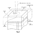
- FIG. 2 shows a state in which the inside of the contour is illuminated.
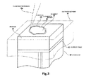
- FIG. 3 shows a state in which the contour is illuminated.
- FIG. 2 The state in which the inside of the contour of the 3D object is illuminated is first described by referring to FIG. 2 .
- the powder 31 tightly spread over the support stage 43 is illuminated with the electron beam B.
- This electron beam B is emitted continuously by supplying electric power to the electron source 11 from a DC power supply and denoted as B c .
- this electron beam emitted continuously is referred to as the continuous electron beam.
- the controller 21 evaluates the positions of a contour 34 formed by slices of the created 3D object.
- the deflector lens controller 27 sets how the electron beam is deflected by the deflector lens 15 such that the continuous electron beam B c scans the region located inside of the evaluated contour 34.
- the deflector lens controller 27 sets how the electron beam is deflected by the deflector lens 15 such that locations along the contour 34 are scanned by the electron beam. That is, as shown in FIG. 3 , the deflector lens controller 27 sets how the electron beam is deflected by the deflector lens 15 such that the electron beam B p makes one revolution along the contour 34.
- the pulsed voltage generator 23 applies a pulsed voltage to the extractor electrode 12.
- the electron source 11 outputs the pulse-like electron beam B p .
- this pulse-like electron beam is referred to as the pulsed electron beam.
- the powder 31 is illuminated with the pulsed electron beam B p .
- the powder 31 at the illuminated locations sublimates and evaporates. Therefore, when illumination by the pulsed electron beam B p for one layer is complete, it follows that a 3D object 33 having one layer of contour 34 has been formed.
- the principle on which the powder 31 illuminated with the pulsed electron beam B p sublimates and evaporates will be described later.
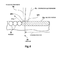
- FIG. 4 is a vertical cross section of the powder 31 illuminated with the electron beam.
- the right side of the contour 34 will form a 3D object, i.e., design positions of the 3D object.
- the left side of the contour 34 will not form any part of the 3D object.
- a position SP1 hit by the continuous electron beam B c is on the right side of the contour 34.
- the inside of the hit position SP2 is coincident with the contour 34. Owing to such illumination by the pulsed electron beam B p , those portions of the powder 31 which are located outside the contour 34 become gas 31a and evaporate off.
- the spot size at the position SP2 hit by the pulsed electron beam B p is smaller than the spot size at the position SP1 hit by the continuous electron beam B c .
- the diameter of each grain of the powder 31 is the same as the thickness of one layer of molten portion 33a of the powder 31. In practice, the thickness of one layer of molten portion 33a may sometimes be greater than the diameter of each grain of the powder 31.
- FIGS. 5A-5F show the characteristics of the continuous electron beam and of the pulsed electron beam.
- FIG. 5A shows variations in the position SP1 hit by the continuous electron beam.
- FIG. 5B shows the position SP2 hit by the pulsed electron beam.
- the hit position moves a distance corresponding to the spot size (diameter of r1) at the hit position SP1.
- the powder is illuminated with a spot size having a diameter of r 2 at some timing. This illumination with the spot size of diameter r2 is done intermittently while varying the position.
- the current I c of the power supplied to the electron source 11 is constant.
- a current I p of a pulse width of a short duration t p is supplied.
- the current I p of the pulse width t p is supplied at regular intervals of time and so pulses of the electron beam are generated at regular intervals.
- the current I p of the pulsed electron beam is greater than the current I c of the continuous electron beam.
- FIGS. 5E and 5F are cross-sectional views of the locations hit by the continuous electron beam and by the pulsed electron beam, showing examples in which the powder 31 is molten by being illuminated with an electron beam.
- FIG. 5E shows a case of the continuous electron beam B c .
- FIG. 5F shows a case of the pulsed electron beam B p .
- the distribution J p of the current density of the electron beam B p hitting the sample surface 32 takes on a shape as shown in FIG. 5F . That is, the current density is quite high only at the hit position. Therefore, when the powder 31 is molten using the pulsed electron beam B p , the actually molten region A p nearly coincident with the planned molten region A1 is obtained. Furthermore, in the additive manufacturing machine 100 according to the present embodiment, the current density distribution J p is appropriately controlled to make the temperature of the sample (i.e., the molten powder 31) higher than the temperature assumed when the sample is being molten, to sublimate and evaporate the sample.
- FIGS. 6A and 6B compare a state ( FIG. 6A ) in which the powder 31 has been molten by illumination by the continuous electron beam B c and a state ( FIG. 6B ) in which the powder 31 has been sublimated by illumination by the pulsed electron beam B p .
- a molten region A in is formed by illumination with the continuous electron beam B c .
- the molten area A in is spread by variation of the position on the sample surface 32 hit by the continuous electron beam B c .
- the continuous electron beam B c melts the powder 31 up to a design end point x that corresponds to the contour 34 shown in FIG. 3 .
- FIG. 6A shows a state in which the design end point x is coincident with an end of the molten region A in .
- the molten region A in may spread slightly outwardly of the design end point x.
- an outside of the design end point x is selected as a sublimated region 35 as shown in FIG. 6B .
- the width of the sublimated region 35 is substantially coincident with the diameter of the spot size of the pulsed electron beam B p .
- the depth of the sublimated region 35 is set nearly equal to the thickness of one layer of the tightly spread powder 31.
- FIGS. 7A and 7B are views taken from above the sample surface 32.
- a sublimated region outside line 35a is set along the contour 34 so as to be spaced a given width from the contour 34.
- the region between the contour 34 and the sublimated region outside line 35a is illuminated with the pulsed electron beam B p of a current density that sublimates the sample such that the beam B p is scanned sequentially across this region.
- V p (t) be the voltage generated by the pulsed voltage generator 23 shown in FIG. 1 when the pulsed electron beam B p is emitted.
- This voltage V p (t) is a pulsed voltage and is 0 (V) or V p (V) at time t.
- V c be the voltage generated by the extraction voltage generator 22 shown in FIG. 1 .
- This voltage V c remains constant irrespective of time and generates the continuous electron beam B c .
- These voltages V p (t) and V c are summed up by the adder 24.
- the sum voltage is applied to the extractor electrode 12. That is, a voltage V e (t) as given by the following Eq. (1) is applied to the extractor electrode 12.
- V e t V p t + V c
- the extraction voltage V e is applied to the extractor electrode 12, increasing the electric field strength around the front end of the electron source 11. As a result, electrons are emitted.
- the continuous electron beam B c or the pulsed electron beam B p is accelerated by a voltage V a that is applied from the accelerating voltage generator 25 to the acceleration electrode 13.
- V e (t) V c
- the brightness B (A/m 2 /sr) of an electron beam is given by the following Eq. (7) and has the property that it is constant along the optical axis.
- B ⁇ p ⁇ r p 2
- ⁇ p the angular current density on the sample surface
- the brightness of the pulsed electron beam is higher than the brightness of the continuous electron beam and, therefore, if the angular current density is constant, the diameter of the continuous electron beam is smaller than the diameter of the pulsed electron beam.
- the continuous electron beam of FIG. 5E and the pulsed electron beam of FIG. 5F show this state.
- the amount of injected energy is the same for both of the continuous electron beam of FIG. 5E and the pulsed electron pulse of FIG. 5F .
- the current density distribution J p shown in FIG. 5F is a current density distribution assumed when the sample is illuminated with one pulse.
- the current density distribution of the pulsed electron beam has a higher peak value and a smaller half-value width.
- the time in which the planned molten region A1 is molten is much shorter in the case of the pulsed electron pulse. That is, where the amount of the injected energy is the same, the spot size at the position SP2 hit by the pulsed electron beam is smaller than the spot size at the position SP1 hit by the continuous electron beam as shown in FIG. 8A . Consequently, in the case of the pulsed electron beam, almost no heat transmission occurs. The sample undergoes no heat damage. The planned molten region A1 and the actually molten region A p are almost equal.
- the continuous electron beam energy is injected for a prolonged time. Heat is propagated to the outside of the planned molten region A1. In some cases, the planned molten region A1 may not be fully molten, resulting in defects. In the case of the continuous electron beam, heat is propagated to the surroundings of the planned molten region A1, causing heat damage to the sample. If a higher energy is injected in an attempt to fully melt the planned molten region A1, it brings broadening the region subjected to heat damage.
- the pulsed electron beam B p when the pulsed electron beam B p is produced, a pulsed voltage to which a bias voltage is added is applied to the extractor electrode 12. That is, as shown in FIG. 8B , when the current I c based on the voltage V c applied by the extraction voltage generator 22 is not 0, the emission current I t (t) is the sum of the current I c and the current I p .
- the current density distribution at the sample surface varies with time. That is, sometimes the current density distribution is the current density distribution of the continuous electron beam, and sometimes the distribution is the sum of the current density distribution of the pulsed electron beam and the current density distribution of the continuous electron beam.
- the bias voltage V c applied by the extraction voltage generator 22 when the pulsed electron beam B p is produced is used for a pretreatment where the powder 31 is not fully molten but the temperature is raised to an appropriate temperature. For example, this pretreatment is performed using only the continuous electron beam. Then, the pulsed voltage V p is added to the bias voltage V c , and the pulsed electron beam is generated to melt or sublimate the powder.
- the current and the pulse width are finely controlled when the pulsed electron beam is used.
- the continuous electron beam current I c , pulse width t p , pulsed voltage V p , and pulse frequency v p may be combined optimally according to conditions used when a three-dimensional object is fabricated such that the additive manufacturing is controlled finely.
- two kinds of currents, I p 1 and I p 2 are selectively used as the current for generating the pulsed electron beam.
- pulse widths t p1 , t p2 , t p3 , t p4 , t p5 , and so forth are varied according to the conditions.
- the additive manufacturing process can be finely controlled by the use of the pulsed electron beam in this way.
- step S11 the controller 21 gives an instruction to spread one layer of the powder 31 tightly over the support stage 43 using the linewise funnel (not shown) (step S11).
- step S12 the controller 21 gives an instruction regarding a voltage to the extraction voltage generator 22 to emit the continuous electron beam (step S12).
- the controller 21 directs the continuous electron beam at the powder 31 located inside of the design ends of the 3D object to melt the powder 31 at the hit positions (step S13).
- the controller 21 makes a decision as to whether the melting of the powder 31 located inside of the design ends of the 3D object is completed (step S14). If the melting of the powder 31 is not complete, the melting operation of step S13 is performed.
- step S 14 If the decision at step S 14 is affirmative to indicate that the melting of the powder 31 inside of the design ends is completed, the controller 21 gives an instruction about a voltage to the pulsed voltage generator 23 such that the pulsed electron beam is emitted (step S15).
- the controller 21 directs the pulsed electron beam at the powder 31 located outside of the design ends of the 3D object and along the design ends to sublimate the powder 31 at the hit positions (step S16).
- the controller 21 makes a decision as to whether the sublimation of the powder portions located along the design ends of the 3D object is completed (step S17). If the sublimation of the powder 31 is not completed, the sublimation operation of step S16 is performed.
- step S 18 the controller 21 makes a decision as to whether the additive manufacturing process is completed (step S18). If the process is not completed, control goes back to step S11, where the operation for tightly spreading the powder 31 to form the next layer is performed. In the additive manufacturing machine 100, the sequence of processing operations from step S11 to step S16 is repeated as many times as there are layers required. If the decision at step S18 is that the additive manufacturing process is completed, the controller 21 ends the operation of the multilayered fabrication for the single 3D object.
- the additive manufacturing machine 100 of the present embodiment can produce an accurate 3D multilayered object using two kinds of beams, i.e., the continuous electron beam and the pulsed electron beam. That is, by forming the contour of the 3D object through sublimation using the pulsed electron beam, the surface roughness of the 3D object does not depend on the grain diameter of the powder 31. Consequently, the surface roughness of the 3D object can be improved. In addition, that the surface roughness of the 3D object does not depend on the grain diameter of the powder 31 makes it unnecessary to reduce the grain diameter of the powder 31. This contributes to improvement of the speed at which additive manufacturing is performed.
- the additive manufacturing machine 100 can perform an accurate additive manufacturing process where the range in which the powder is molten or sublimated by the pulsed electron beam is substantially coincident with the beam diameter by performing the process through the use of the pulsed electron beam.
- the pulsed electron beam is used when the powder is sublimated.
- the pulsed electron beam may melt the powder by setting the current of the pulsed electron beam to such an extent as to melt the powder.
- the addition of a constant bias voltage to the pulsed voltage for producing the pulsed electron beam can better the additive manufacturing process.
- a voltage, for example, for heating the powder on the bias voltage there arises the advantage that the pulsed electron beam can be emitted while performing the heating operation.
- the pulsed electron beam is used when the powder is sublimated.
- the pulsed electron beam may be used when the powder is molten. That is, when the powder portions located inside the contour line of a 3D object to be fabricated are molten, the electron source 11 may direct a pulsed electron beam at the powder 31.
- the controller 21 can more accurately define the molten region by using the pulsed electron beam in this way.
- the process for sublimating the outside of the contour constitutes only one example.
- the pulsed electron beam may be used only to melt the powder.
- a 3D multilayered object may be fabricated without performing sublimation.
- the process for superimposing the voltage for heating the powder on the pulsed voltage constitutes only one example.
- the bias voltage for heating purposes may not be superimposed.
- the above-described embodiment is the additive manufacturing machine having the electron source 11 emitting an electron beam at the powder 31.
- the additive manufacturing machine of the present invention may also be applied to other machine having other beam generator producing a laser beam.
- a continuous laser beam and a pulsed laser beam are prepared as laser beams.
- the outside of the contour of a 3D object is sublimated using the pulsed laser beam.
- lenses other than the objective lens 14 and the deflector lens 15 may be mounted in locations through which the electron beam B passes.
Landscapes
- Engineering & Computer Science (AREA)
- Chemical & Material Sciences (AREA)
- Materials Engineering (AREA)
- Manufacturing & Machinery (AREA)
- Mechanical Engineering (AREA)
- Physics & Mathematics (AREA)
- Toxicology (AREA)
- General Health & Medical Sciences (AREA)
- Health & Medical Sciences (AREA)
- Optics & Photonics (AREA)
- Plasma & Fusion (AREA)
- Automation & Control Theory (AREA)
- Ceramic Engineering (AREA)
- Analytical Chemistry (AREA)
- Powder Metallurgy (AREA)
Abstract
Description
- The present invention relates to a machine and method for 'additive manufacturing', fabricating a three-dimensional object by illuminating a layer of a powdered material with a beam to form a solidified layer and repeating this process.
- In recent years, techniques for fabricating a three-dimensional (3D) object by creating two-dimensional data about slices of a given thickness of the 3D object from data about the 3D object, forming a solidified layer based on the two-dimensional data, and repeating this process have been developed (see patent document 1).
- In such an additive manufacturing machine for fabricating a three-dimensional object, a powdered material for one layer is first supplied onto a support stage capable of moving up and down. A beam generator emits an electron beam or laser beam at the layer of the powdered material. At this time, the powdered material at a given position is molten by the beam by illuminating the powdered material with the beam while scanning the beam within a two-dimensional plane. Since the powdered material is molten, the molten grains of the powdered material bond together. The material is then cooled and solidified. As a result, one layer of solidified material is formed. Then, the support stage is lowered and additional powdered material is supplied. The powdered material is molten and solidified in the same way as in the previous steps. As a result, a second layer of solidified material is formed integrally with the previously formed, lower layer of solidified material. In this way, the support stage is lowered an incremental distance. A powdered material is supplied onto the stage. The powdered material is molten and solidified. This series of steps is repeated. Consequently, a three-dimensional object is fabricated.
- Patent document 1:
JP-A-2001-152204 - The accuracy at which a three-dimensional object is fabricated by an additive manufacturing machine depends on the grain diameter of the powdered material and on the diameter of the illuminating beam. That is, it is desirable to reduce the grain diameter of the powdered material as much as possible in enhancing the accuracy of additive manufacturing. However, if the grain diameter of the powdered material is reduced, the thickness of each one layer of powdered material spread tightly on a support stage decreases. In this case, the number of layers of spread powdered material necessary to fabricate a three-dimensional (3D) object is increased. This in turn prolongs the time taken to fabricate the 3D object. In this way, it is not always desirable to reduce the grain diameter of the powdered material as much as possible.
- Accordingly, the accuracy at which a three-dimensional multilayered object is fabricated depends strongly on the diameter of the illuminating beam. A major factor determining the accuracy at which a three-dimensional (3D) multilayered object is fabricated is the contour of the 3D object. Where it is assumed that the contour of the 3D object perfectly coincides with the positions scanned by the illuminating beam, if the scanning of the illuminating beam is improved, then the accuracy at which the contour of the 3D multilayered object is formed is improved.
- In practice, however, when a powdered material is illuminated with a beam, heat of solution that is conducted through the powdered material is produced. As a result, even surroundings of the illuminated spots are molten. In this circumstance, the positions hit by the beam does not agree with the contour of the 3D object. Since melting and bonding of the grains of the powdered material through the conduction of the heat of solution is determined probabilistically, melting of even the surroundings of the illuminated spots will deteriorate the accuracy at which the contour of the 3D multilayered object is formed. This gives rise to a factor impairing the surface roughness of the 3D multilayered object.
- The problems occurring when the contour of a three-dimensional multilayered object is formed have been described so far. When a beam scans locations other than the contour, it is important that the positions scanned by the beam agree with locations at which grains of a powdered material are molten and bonded together in enhancing the accuracy of additive manufacturing.
- It would be desirable to provide a machine and method for additive manufacturing capable of precisely controlling locations at which a powdered material is molten by a beam.
- According to the present invention, there is provided additive manufacturing machines as set out in
claims 1 and 7 and methods of fabricating a three-dimensional multilayered object as set out inclaims - An additive manufacturing machine according to a first embodiment of the present invention has a support stage on which a powdered material is spread tightly, a beam generator producing a beam, a lens for focusing the beam produced by the beam generator onto the powdered material spread on the support stage, and a controller for controlling the beam generator. The controller causes the beam generator to selectively produce two kinds of beams, i.e., a continuous beam and a pulsed beam.
- An additive manufacturing method according to a second embodiment of the present invention starts with spreading a powdered material tightly on a support stage. The material is illuminated with a beam to melt and bond together grains of the powdered material to obtain a 3D multilayered object. Two kinds of beams, i.e., a continuous beam and a pulsed beam, are selectively produced as the illuminating beam.
- An additive manufacturing machine according to a third embodiment of the present invention has a support stage on which a powdered material is spread tightly, an electron gun producing an electron beam, a lens for focusing the electron beam produced by the electron gun onto the powdered material spread on the support stage, and a controller for controlling the electron gun. The controller causes the electron gun to generate a pulsed beam of electrons.
- An additive manufacturing method according to a fourth embodiment of the present invention starts with spreading a powdered material tightly on a support stage. The material is illuminated with an electron beam to melt and cure the powdered material, thus obtaining a three-dimensional object. The electron beam produced by the electron gun is a pulsed beam and used to melt or sublimate the powdered material.
- According to the first or second embodiment, a three-dimensional multilayered object can be obtained by using two kinds of beams, i.e., a continuous beam and a pulsed beam. The surface roughness of the additive manufacturing object can be improved and, at the same time, the speed at which the additive manufacturing object is produced can be increased, for example, by using the pulsed beam in forming the contour of the object and using the continuous beam in forming object portions other than the contour.
- According to the third or fourth embodiment of the present invention, the pulsed electron beam is used as the electron beam used to obtain a three-dimensional multilayered object by melting and bonding together grains of a powdered material. Thus, an accurate additive manufacturing process can be performed in such a way that the beam diameter is substantially coincident with the range in which the material is molten. Consequently, the accuracy at which a three-dimensional multilayered object is fabricated can be improved.
-
-
FIG. 1 is a schematic vertical cross section, partly in block form, of an additive manufacturing machine according to one embodiment of the present invention, showing the whole configuration of the machine. -
FIG. 2 is a fragmentary perspective view of the additive manufacturing machine shown inFIG. 1 , and in which a material is being illuminated with a beam to form the inside of the contour of a 3D object. -
FIG. 3 is a fragmentary perspective view similar toFIG. 2 , but showing the manner in which the material is being illuminated with a beam to form the contour. -
FIG. 4 is an explanatory view showing the manner in which powder is molten and sublimated by illuminating the inside of design positions of a 3D object with a beam and illuminating the contour with a beam in accordance with one embodiment of the invention. -
FIGS. 5A, 5C, and 5E are explanatory views of examples of characteristics of a continuous electron beam. -
FIGS. 5B, 5D, and 5F are explanatory views of examples of characteristics of a pulsed electron beam. -
FIG. 6A is an explanatory view showing the manner in which powder is being illuminated with a continuous beam in accordance with one embodiment of the invention. -
FIG. 6B is an explanatory view showing the manner in which powder is being illuminated with a pulsed beam in accordance with one embodiment of the invention. -
FIGS. 7A and 7B are explanatory views showing examples of positions illuminated with a pulsed beam to form a contour line in accordance with one embodiment of the invention.FIG. 8A is a view illustrating the diameters of a continuous beam and of a pulsed beam in accordance with one embodiment of the invention. -
FIGS. 8B and 8C are graphs showing examples of drive currents for the pulsed beam. -
FIG. 9 is a flowchart illustrating one example of a layer-wise additive manufacturing process sequence in accordance with one embodiment of the invention. - An additive manufacturing machine according to one embodiment of the present invention is hereinafter described with reference to the accompanying drawings.
-
FIG. 1 schematically shows the configuration of the additive manufacturing machine, 100, according to one embodiment of the invention. Themachine 100 has anelectron source 11 emitting an electron beam B.An extractor electrode 12 and anacceleration electrode 13 are disposed near theelectron source 11. Theelectron source 11,extractor electrode 12, andacceleration electrode 13 together operate as an electron gun generating and accelerating the electron beam. - Voltages are applied to the
electron source 11,extractor electrode 12, andacceleration electrode 13 under control of acontroller 21. In particular, anextraction voltage generator 22 generates an extraction voltage applied to theextractor electrode 12 under instructions from thecontroller 21. The extraction voltage generated by theextraction voltage generator 22 is an extraction voltage for a continuous electron beam (described later). Apulsed voltage generator 23 generates a pulsed voltage applied to theextractor electrode 12 under instructions from thecontroller 21. The pulsed voltage generated by thepulsed voltage generator 23 is an extraction voltage for a pulsed electron beam (described later). - The extraction voltage generated by the
extraction voltage generator 22 and used for the continuous electron beam and the extraction voltage generated by thepulsed voltage generator 23 and used for the pulsed electron beam are supplied to theextractor electrode 12 via anadder 24. When thepulsed voltage generator 23 produces the pulsed electron beam, theextraction voltage generator 22 may produce a bias voltage (described later) for heating apowder 31. An acceleratingvoltage generator 25 generates an accelerating voltage applied to theacceleration electrode 13 under instructions from thecontroller 21. The accelerating voltage generated by the acceleratingvoltage generator 25 is impressed on theacceleration electrode 13. When theelectron source 11 produces an electron beam, theelectron source 11 is heated by a heater (not shown). - The electron beam B emitted from the
electron source 11 is directed at thepowder 31 spread tightly on asupport stage 43. Thepowder 31 is spread tightly on thestage 43 to a given thickness by a linewise funnel (not shown). The electron beam B produced from theelectron source 11 passes through anobjective lens 14 and adeflector lens 15 and reaches thepowder 31. Each of theobjective lens 14 anddeflector lens 15 is an electromagnetic lens producing an electric or magnetic field acting on the electron beam. - The
objective lens 14 focuses the electron beam B onto thepowder 31 located on thesupport stage 43 under control of anobjective lens controller 26 that is controlled based on instructions from thecontroller 21. Thedeflector lens 15 deflects the electron beam B such that the electron beam B illuminates positions corresponding to the sliced shape of the 3D multilayered object to be fabricated. Thedeflector lens 15 operates to deflect the electron beam under control of adeflector lens controller 27 that is controlled based on instructions from thecontroller 21. - The
support stage 43 is disposed in acentral pit 42 formed in asupport platform 41 and can move up and down. In an interlocking manner with the formation of each layer of thepowder 31, thesupport stage 43 descends an incremental distance corresponding to the thickness of each layer. After one layer of thepowder 31 is spread tightly on thesupport stage 43, thepowder 31 is molten by the electron beam B in conformity with the shape of the 3D multilayered object to be fabricated. In the present embodiment, an operation for sublimating thepowder 31 is performed apart from the operation for melting the powder. - The
additive manufacturing machine 1 performs the operation for tightly spreading thepowder 31 in a layer-wise manner, the layer-wise operation for melting thepowder 31, and the layer-wise operation for sublimating thepowder 31 repeatedly to fabricate a three-dimensional object. The operation for illuminating the powder with the electron beam B is performed after the interior of the additive manufacturing machine shown inFIG. 1 has been evacuated by a vacuum pump (not shown). - How powder is illuminated with a beam by the additive manufacturing machine according to one embodiment of the present invention is next described by referring to
FIGS. 2-4 . With theadditive manufacturing machine 100 according to one embodiment of the invention, processing steps for illuminating thepowder 31 with the electron beam B include two steps, i.e., a step of illuminating the contour of the 3D object and a step of illuminating the inside of the contour.FIG. 2 shows a state in which the inside of the contour is illuminated.FIG. 3 shows a state in which the contour is illuminated. - The state in which the inside of the contour of the 3D object is illuminated is first described by referring to
FIG. 2 . As shown in this figure, thepowder 31 tightly spread over thesupport stage 43 is illuminated with the electron beam B. This electron beam B is emitted continuously by supplying electric power to theelectron source 11 from a DC power supply and denoted as Bc. In the following description, this electron beam emitted continuously is referred to as the continuous electron beam. Grains of thepowder 31 at the locations hit by the continuous electron beam Bc melt and bond together. - When the
powder 31 is illuminated with the electron beam, thecontroller 21 evaluates the positions of acontour 34 formed by slices of the created 3D object. Thedeflector lens controller 27 sets how the electron beam is deflected by thedeflector lens 15 such that the continuous electron beam Bc scans the region located inside of the evaluatedcontour 34. - When the illumination of the inside of the
contour 34 with the continuous electron beam is complete, thedeflector lens controller 27 sets how the electron beam is deflected by thedeflector lens 15 such that locations along thecontour 34 are scanned by the electron beam. That is, as shown inFIG. 3 , thedeflector lens controller 27 sets how the electron beam is deflected by thedeflector lens 15 such that the electron beam Bp makes one revolution along thecontour 34. At this time, thepulsed voltage generator 23 applies a pulsed voltage to theextractor electrode 12. As a result, theelectron source 11 outputs the pulse-like electron beam Bp. In the following description, this pulse-like electron beam is referred to as the pulsed electron beam. - The
powder 31 is illuminated with the pulsed electron beam Bp. Thepowder 31 at the illuminated locations sublimates and evaporates. Therefore, when illumination by the pulsed electron beam Bp for one layer is complete, it follows that a3D object 33 having one layer ofcontour 34 has been formed. The principle on which thepowder 31 illuminated with the pulsed electron beam Bp sublimates and evaporates will be described later. -
FIG. 4 is a vertical cross section of thepowder 31 illuminated with the electron beam. In the example ofFIG. 4 , the right side of thecontour 34 will form a 3D object, i.e., design positions of the 3D object. The left side of thecontour 34 will not form any part of the 3D object. A position SP1 hit by the continuous electron beam Bc is on the right side of thecontour 34. With respect to another position SP2 hit by the pulsed electron beam Bp, the inside of the hit position SP2 is coincident with thecontour 34. Owing to such illumination by the pulsed electron beam Bp, those portions of thepowder 31 which are located outside thecontour 34 becomegas 31a and evaporate off. - The spot size at the position SP2 hit by the pulsed electron beam Bp is smaller than the spot size at the position SP1 hit by the continuous electron beam Bc. In
FIG. 4 , for the sake of simplicity of explanation, it is assumed that the diameter of each grain of thepowder 31 is the same as the thickness of one layer ofmolten portion 33a of thepowder 31. In practice, the thickness of one layer ofmolten portion 33a may sometimes be greater than the diameter of each grain of thepowder 31. - The characteristics of the continuous electron beam and of the pulsed electron beam are next described by referring to
FIGS. 5-8 .FIGS. 5A-5F show the characteristics of the continuous electron beam and of the pulsed electron beam.FIG. 5A shows variations in the position SP1 hit by the continuous electron beam.FIG. 5B shows the position SP2 hit by the pulsed electron beam. With respect to the continuous electron beam, as shown inFIG. 5A , when time tc01 elapses, the hit position moves a distance corresponding to the spot size (diameter of r1) at the hit position SP1. On the other hand, with respect to the pulsed electron beam, as shown inFIG. 5B , the powder is illuminated with a spot size having a diameter of r2 at some timing. This illumination with the spot size of diameter r2 is done intermittently while varying the position. - As shown in
FIG. 5C , in the case of the continuous electron beam, the current Ic of the power supplied to theelectron source 11 is constant. On the other hand, in the case of the pulsed electron beam, a current Ip of a pulse width of a short duration tp is supplied. The current Ip of the pulse width tp is supplied at regular intervals of time and so pulses of the electron beam are generated at regular intervals. The current Ip of the pulsed electron beam is greater than the current Ic of the continuous electron beam. -
FIGS. 5E and 5F are cross-sectional views of the locations hit by the continuous electron beam and by the pulsed electron beam, showing examples in which thepowder 31 is molten by being illuminated with an electron beam.FIG. 5E shows a case of the continuous electron beam Bc.FIG. 5F shows a case of the pulsed electron beam Bp. - In the case of the continuous electron beam Bc, the current density distribution Jc of the electron beam Bc hitting a
sample surface 32 is spread over a relatively large area as shown inFIG. 5E . Therefore, if a planned molten region A1 where thepowder 31 should be molten is substantially coincident with the spot size of the continuous electron beam Bc, an actually molten region Ac where thepowder 31 is actually molten spreads far from the spot size. Thepowder 31 is molten in regions where the powder should not be molten. - On the other hand, in the case of the pulsed electron beam Bp, the distribution Jp of the current density of the electron beam Bp hitting the
sample surface 32 takes on a shape as shown inFIG. 5F . That is, the current density is quite high only at the hit position. Therefore, when thepowder 31 is molten using the pulsed electron beam Bp, the actually molten region Ap nearly coincident with the planned molten region A1 is obtained. Furthermore, in theadditive manufacturing machine 100 according to the present embodiment, the current density distribution Jp is appropriately controlled to make the temperature of the sample (i.e., the molten powder 31) higher than the temperature assumed when the sample is being molten, to sublimate and evaporate the sample. -
FIGS. 6A and 6B compare a state (FIG. 6A ) in which thepowder 31 has been molten by illumination by the continuous electron beam Bc and a state (FIG. 6B ) in which thepowder 31 has been sublimated by illumination by the pulsed electron beam Bp. As shown inFIG. 6A , a molten region Ain is formed by illumination with the continuous electron beam Bc. The molten area Ain is spread by variation of the position on thesample surface 32 hit by the continuous electron beam Bc. At this time, the continuous electron beam Bc melts thepowder 31 up to a design end point x that corresponds to thecontour 34 shown inFIG. 3 .FIG. 6A shows a state in which the design end point x is coincident with an end of the molten region Ain. The molten region Ain may spread slightly outwardly of the design end point x. - When the pulsed electron beam Bp is emitted, an outside of the design end point x is selected as a sublimated
region 35 as shown inFIG. 6B . The width of the sublimatedregion 35 is substantially coincident with the diameter of the spot size of the pulsed electron beam Bp. The depth of the sublimatedregion 35 is set nearly equal to the thickness of one layer of the tightly spreadpowder 31. -
FIGS. 7A and 7B are views taken from above thesample surface 32. As shown inFIG. 7A , after the continuous electron beam Bc has melted thepowder 31 up to thecontour 34, a sublimated region outsideline 35a is set along thecontour 34 so as to be spaced a given width from thecontour 34. Then, as shown inFIG. 7B , the region between thecontour 34 and the sublimated region outsideline 35a is illuminated with the pulsed electron beam Bp of a current density that sublimates the sample such that the beam Bp is scanned sequentially across this region. - The characteristics of the pulsed electron beam Bp are next described. Let Vp (t) be the voltage generated by the
pulsed voltage generator 23 shown inFIG. 1 when the pulsed electron beam Bp is emitted. This voltage Vp (t) is a pulsed voltage and is 0 (V) or Vp (V) at time t. Let Vc be the voltage generated by theextraction voltage generator 22 shown inFIG. 1 . This voltage Vc remains constant irrespective of time and generates the continuous electron beam Bc. These voltages Vp (t) and Vc are summed up by theadder 24. The sum voltage is applied to theextractor electrode 12. That is, a voltage Ve (t) as given by the following Eq. (1) is applied to theextractor electrode 12.
- The extraction voltage Ve is applied to the
extractor electrode 12, increasing the electric field strength around the front end of theelectron source 11. As a result, electrons are emitted. The continuous electron beam Bc or the pulsed electron beam Bp is accelerated by a voltage Va that is applied from the acceleratingvoltage generator 25 to theacceleration electrode 13. When the continuous electron beam Bc is emitted, the extraction voltage Ve (t) is given by
- That is, when the continuous electron beam Bc is being generated, the constant voltage Vc is kept applied to the
extractor electrode 12 and the continuous electron beam Bc of constant current Ic is being emitted. There is a linear relationship between the emission current and the extraction voltage Ve (t). The emission current, It (t), is given by
where Ic is an emission current corresponding to the voltage Vc, Ip is an emission current corresponding to the voltage Vp (t), and tp is the pulse width. - That is, the emission current It (t) can be a function of time. This function can be varied by the current Ic, pulse width tp, peak pulsed voltage Vp, and pulse frequency vp as shown in
FIG. 8C , and is given by
- Energy E injected into the powdered sample by electron beam illumination is given by

- It can be seen from Eqs. (4) and (5) that the amount of energy injected into the sample can be controlled by four parameters i.e., Ic, tp, Vp, and vp. When it is assumed that Ic = 0, the emission current It (t) is represented as shown in
FIG. 5D . It is assumed that the sample is illuminated with only one pulse shown inFIG. 5D and that the injected energy gives an equality as given by Eq. (6). That is, an area determined by both the duration of the interval tc01 and the current while the continuous current shown inFIG. 5C is being supplied is equal to an area determined by both the pulse interval tp shown inFIG. 5D and the current.
- The brightness B (A/m2/sr) of an electron beam is given by the following Eq. (7) and has the property that it is constant along the optical axis.

where βp is the angular current density on the sample surface and rp is the diameter of the pulsed electron beam on the sample surface. Therefore, the diameter rp of the pulsed electron beam Bp is given by
- Usually, the brightness of the pulsed electron beam is higher than the brightness of the continuous electron beam and, therefore, if the angular current density is constant, the diameter of the continuous electron beam is smaller than the diameter of the pulsed electron beam. The continuous electron beam of
FIG. 5E and the pulsed electron beam ofFIG. 5F show this state. The amount of injected energy is the same for both of the continuous electron beam ofFIG. 5E and the pulsed electron pulse ofFIG. 5F . The current density distribution Jp shown inFIG. 5F is a current density distribution assumed when the sample is illuminated with one pulse. - As can be seen by comparison of
FIGS. 5E and 5F , the current density distribution of the pulsed electron beam has a higher peak value and a smaller half-value width. Although the amount of the injected energy is the same in this case, the time in which the planned molten region A1 is molten is much shorter in the case of the pulsed electron pulse. That is, where the amount of the injected energy is the same, the spot size at the position SP2 hit by the pulsed electron beam is smaller than the spot size at the position SP1 hit by the continuous electron beam as shown inFIG. 8A . Consequently, in the case of the pulsed electron beam, almost no heat transmission occurs. The sample undergoes no heat damage. The planned molten region A1 and the actually molten region Ap are almost equal. - In the case of the continuous electron beam, energy is injected for a prolonged time. Heat is propagated to the outside of the planned molten region A1. In some cases, the planned molten region A1 may not be fully molten, resulting in defects. In the case of the continuous electron beam, heat is propagated to the surroundings of the planned molten region A1, causing heat damage to the sample. If a higher energy is injected in an attempt to fully melt the planned molten region A1, it brings broadening the region subjected to heat damage.
- In the
additive manufacturing machine 100, when the pulsed electron beam Bp is produced, a pulsed voltage to which a bias voltage is added is applied to theextractor electrode 12. That is, as shown inFIG. 8B , when the current Ic based on the voltage Vc applied by theextraction voltage generator 22 is not 0, the emission current It (t) is the sum of the current Ic and the current Ip. At this time, the current density distribution at the sample surface varies with time. That is, sometimes the current density distribution is the current density distribution of the continuous electron beam, and sometimes the distribution is the sum of the current density distribution of the pulsed electron beam and the current density distribution of the continuous electron beam. - The bias voltage Vc applied by the
extraction voltage generator 22 when the pulsed electron beam Bp is produced is used for a pretreatment where thepowder 31 is not fully molten but the temperature is raised to an appropriate temperature. For example, this pretreatment is performed using only the continuous electron beam. Then, the pulsed voltage Vp is added to the bias voltage Vc, and the pulsed electron beam is generated to melt or sublimate the powder. - In the example of
FIG. 8C , the current and the pulse width are finely controlled when the pulsed electron beam is used. Specifically, as shown inFIG. 8C , the continuous electron beam current Ic, pulse width tp, pulsed voltage Vp, and pulse frequency vp may be combined optimally according to conditions used when a three-dimensional object is fabricated such that the additive manufacturing is controlled finely. In the example ofFIG. 8C , two kinds of currents, Ip1 and Ip2, are selectively used as the current for generating the pulsed electron beam. Furthermore, pulse widths tp1, tp2, tp3, tp4, tp5, and so forth are varied according to the conditions. The additive manufacturing process can be finely controlled by the use of the pulsed electron beam in this way. - An example of control operation performed by the
controller 21 when a 3D object is fabricated by theadditive manufacturing machine 100 according to one embodiment of the present invention is next described by referring to the flowchart ofFIG. 9 . First, thecontroller 21 gives an instruction to spread one layer of thepowder 31 tightly over thesupport stage 43 using the linewise funnel (not shown) (step S11). When this spreading operation is complete, thecontroller 21 gives an instruction regarding a voltage to theextraction voltage generator 22 to emit the continuous electron beam (step S12). - The
controller 21 directs the continuous electron beam at thepowder 31 located inside of the design ends of the 3D object to melt thepowder 31 at the hit positions (step S13). Thecontroller 21 makes a decision as to whether the melting of thepowder 31 located inside of the design ends of the 3D object is completed (step S14). If the melting of thepowder 31 is not complete, the melting operation of step S13 is performed. - If the decision at step S 14 is affirmative to indicate that the melting of the
powder 31 inside of the design ends is completed, thecontroller 21 gives an instruction about a voltage to thepulsed voltage generator 23 such that the pulsed electron beam is emitted (step S15). Thecontroller 21 directs the pulsed electron beam at thepowder 31 located outside of the design ends of the 3D object and along the design ends to sublimate thepowder 31 at the hit positions (step S16). Thecontroller 21 makes a decision as to whether the sublimation of the powder portions located along the design ends of the 3D object is completed (step S17). If the sublimation of thepowder 31 is not completed, the sublimation operation of step S16 is performed. - If the decision at step S 17 is affirmative to indicate that the sublimation of the powder portions present along the design ends is completed, the
controller 21 makes a decision as to whether the additive manufacturing process is completed (step S18). If the process is not completed, control goes back to step S11, where the operation for tightly spreading thepowder 31 to form the next layer is performed. In theadditive manufacturing machine 100, the sequence of processing operations from step S11 to step S16 is repeated as many times as there are layers required. If the decision at step S18 is that the additive manufacturing process is completed, thecontroller 21 ends the operation of the multilayered fabrication for the single 3D object. - As described so far, the
additive manufacturing machine 100 of the present embodiment can produce an accurate 3D multilayered object using two kinds of beams, i.e., the continuous electron beam and the pulsed electron beam. That is, by forming the contour of the 3D object through sublimation using the pulsed electron beam, the surface roughness of the 3D object does not depend on the grain diameter of thepowder 31. Consequently, the surface roughness of the 3D object can be improved. In addition, that the surface roughness of the 3D object does not depend on the grain diameter of thepowder 31 makes it unnecessary to reduce the grain diameter of thepowder 31. This contributes to improvement of the speed at which additive manufacturing is performed. - Furthermore, the
additive manufacturing machine 100 according to the present embodiment can perform an accurate additive manufacturing process where the range in which the powder is molten or sublimated by the pulsed electron beam is substantially coincident with the beam diameter by performing the process through the use of the pulsed electron beam. As a result, the accuracy at which a 3D multilayered object is fabricated can be improved. In the present embodiment described so far, the pulsed electron beam is used when the powder is sublimated. Alternatively, the pulsed electron beam may melt the powder by setting the current of the pulsed electron beam to such an extent as to melt the powder. - Additionally, the addition of a constant bias voltage to the pulsed voltage for producing the pulsed electron beam can better the additive manufacturing process. By superimposing a voltage, for example, for heating the powder on the bias voltage, there arises the advantage that the pulsed electron beam can be emitted while performing the heating operation.
- In the additive manufacturing machine according to the above embodiment, the pulsed electron beam is used when the powder is sublimated. Alternatively, the pulsed electron beam may be used when the powder is molten. That is, when the powder portions located inside the contour line of a 3D object to be fabricated are molten, the
electron source 11 may direct a pulsed electron beam at thepowder 31. Thecontroller 21 can more accurately define the molten region by using the pulsed electron beam in this way. - Furthermore, the process for sublimating the outside of the contour constitutes only one example. Alternatively, the pulsed electron beam may be used only to melt the powder. A 3D multilayered object may be fabricated without performing sublimation.
- Further, the process for superimposing the voltage for heating the powder on the pulsed voltage constitutes only one example. The bias voltage for heating purposes may not be superimposed.
- The above-described embodiment is the additive manufacturing machine having the
electron source 11 emitting an electron beam at thepowder 31. The additive manufacturing machine of the present invention may also be applied to other machine having other beam generator producing a laser beam. For example, in the case of an additive manufacturing machine emitting a laser beam at powder, a continuous laser beam and a pulsed laser beam are prepared as laser beams. The outside of the contour of a 3D object is sublimated using the pulsed laser beam. - It is to be understood that the configurations of the various parts of the additive manufacturing machine shown in the above embodiment are merely exemplary and that the present invention is not restricted thereto. For example, in the configurations shown in
FIG. 1 , lenses other than theobjective lens 14 and thedeflector lens 15 may be mounted in locations through which the electron beam B passes.
Claims (12)
- An additive manufacturing machine comprising:a support stage on which a powdered material is spread tightly;a beam generator producing a beam;a lens for focusing the beam produced by the beam generator onto the powdered material spread on the support stage; anda controller for causing the beam generator to produce a pulsed beam as the beam produced by the beam generator.
- The additive manufacturing machine of claims 1 wherein the beam generator is an electron gun and the beam is an electron beam.
- The additive manufacturing machine of claim 1 or 2 where the controller is for causing the beam generator to selectively produce a continuous beam and a pulsed beam as the beam produced by the beam generator.
- An additive manufacturing machine as set forth in claim 3, wherein said controller melts said powdered material by illuminating the powdered material with said continuous beam and sublimates the powdered material by illuminating the powdered material with said pulsed beam.
- An additive manufacturing machine as set forth in claim 4, wherein said controller controls said lens such that a diameter of the beam used when the powdered material is sublimated is smaller than a diameter of the beam used when the powdered material is molten.
- An additive manufacturing machine as set forth in claim 1, wherein said beam generator is an electron gun producing an electron beam, and wherein the electron gun selectively produces a continuous electron beam and a pulsed electron beam under control of said controller.
- An additive manufacturing machine comprising:a support stage on which a powdered material is spread tightly;an electron gun producing an electron beam;a lens for focusing the electron beam produced by the electron gun onto the powdered material spread on the support stage; anda controller for causing the electron gun to produce a pulsed electron beam as the electron beam produced by the electron gun.
- An additive manufacturing machine as set forth in claim 7, wherein said controller melts or sublimates the powdered material by illuminating the powdered material with said pulsed electron beam.
- An additive manufacturing machine as set forth in claim 8, wherein said controller supplies a drive voltage to said electron gun, the drive voltage being produced by superimposing a pulsed voltage on an offset voltage for heating the electron gun.
- An additive manufacturing machine as set forth in claim 9, wherein each pulse of said pulsed electron beam has a duration shorter than 1 microsecond.
- A method of fabricating a three-dimensional multilayered object by spreading a powdered material tightly on a support stage, illuminating the powdered material with a beam, and melting and bonding together grains of the powdered material to obtain the three-dimensional object, said method comprising the step of:selectively producing a continuous beam and a pulsed beam as the illuminating beam.
- A method of fabricating a three-dimensional multilayered object by spreading a powdered material tightly on a support stage and illuminating the powdered material with an electron beam from an electron gun to melt and cure the powdered material, said method comprising the step of:producing a pulsed beam as the electron beam produced by the electron gun to melt or sublimate the powdered material.
Applications Claiming Priority (1)
| Application Number | Priority Date | Filing Date | Title |
|---|---|---|---|
| JP2014046686A JP2015168228A (en) | 2014-03-10 | 2014-03-10 | Apparatus and method for molding three-dimensional laminate |
Publications (1)
| Publication Number | Publication Date |
|---|---|
| EP2918396A1 true EP2918396A1 (en) | 2015-09-16 |
Family
ID=52813889
Family Applications (1)
| Application Number | Title | Priority Date | Filing Date |
|---|---|---|---|
| EP15158295.4A Withdrawn EP2918396A1 (en) | 2014-03-10 | 2015-03-09 | Machine and method for additive manufacturing |
Country Status (3)
| Country | Link |
|---|---|
| US (1) | US20150306699A1 (en) |
| EP (1) | EP2918396A1 (en) |
| JP (1) | JP2015168228A (en) |
Cited By (9)
| Publication number | Priority date | Publication date | Assignee | Title |
|---|---|---|---|---|
| CN107283595A (en) * | 2017-06-28 | 2017-10-24 | 山东中科智能设备有限公司 | It is a kind of to realize that following for large scale semifluid slurry 3D printing changes quick material-changing device |
| WO2018133799A1 (en) * | 2017-01-22 | 2018-07-26 | 清华大学 | Additive manufacturing equipment utilizing combined electron beam selective melting and electron beam butting |
| CN108788144A (en) * | 2017-04-28 | 2018-11-13 | 戴弗根特技术有限公司 | Scattering in increasing material manufacturing is reduced |
| WO2018217646A1 (en) | 2017-05-22 | 2018-11-29 | Howmedica Osteonics Corp. | Device for in-situ fabrication process monitoring and feedback control of an electron beam additive manufacturing process |
| WO2018229085A1 (en) | 2017-06-13 | 2018-12-20 | Musevic Natasa | A machine and a method for additive manufacturing of three-dimensional objects |
| CN109963685A (en) * | 2016-11-16 | 2019-07-02 | 康明斯有限公司 | System and method for adding material to castings |
| CN110076875A (en) * | 2019-04-30 | 2019-08-02 | 广州上龙智能科技有限公司 | A kind of 3D agglomerating plant |
| EP3597333A1 (en) | 2018-07-19 | 2020-01-22 | Howmedica Osteonics Corporation | System and process for in-process electron beam profile and location analyses |
| WO2020096558A1 (en) * | 2018-11-06 | 2020-05-14 | Joint Stock Company "Nvo "Chervona Hvilya" | System for manufacturing of three dimensional objects |
Families Citing this family (21)
| Publication number | Priority date | Publication date | Assignee | Title |
|---|---|---|---|---|
| JP6210493B2 (en) * | 2014-03-14 | 2017-10-11 | 日本電子株式会社 | Charged particle beam irradiation apparatus and charged particle beam irradiation method |
| US10449606B2 (en) * | 2015-06-19 | 2019-10-22 | General Electric Company | Additive manufacturing apparatus and method for large components |
| US11478983B2 (en) | 2015-06-19 | 2022-10-25 | General Electric Company | Additive manufacturing apparatus and method for large components |
| US10610930B2 (en) * | 2015-11-18 | 2020-04-07 | Arcam Ab | Additive manufacturing of three-dimensional articles |
| CN107866631B (en) * | 2016-09-23 | 2020-05-05 | 中国航空制造技术研究院 | A device and method for grain refinement based on electron beam fuse forming |
| US11911838B2 (en) * | 2017-03-10 | 2024-02-27 | Pro-Beam Gmbh & Co. Kgaa | Electron beam installation and method for working powdered material |
| US10758976B2 (en) | 2017-06-21 | 2020-09-01 | General Electric Company | Systems and methods for powder pretreatment in additive manufacturing |
| DE102017120938A1 (en) * | 2017-09-11 | 2019-03-14 | Fraunhofer-Gesellschaft zur Förderung der angewandten Forschung e.V. | Process for coating a substrate and apparatus for carrying out the process |
| DE102017220153A1 (en) * | 2017-11-13 | 2019-06-19 | Trumpf Laser- Und Systemtechnik Gmbh | Method and device for the layered additive manufacturing of components by means of a continuous and a pulsed laser beam and associated computer program product |
| US11426818B2 (en) | 2018-08-10 | 2022-08-30 | The Research Foundation for the State University | Additive manufacturing processes and additively manufactured products |
| KR102188554B1 (en) * | 2019-01-22 | 2020-12-09 | 주식회사 디이엔티 | Laser head optical axis distance adjustment device of metal 3D printer |
| JP7222257B2 (en) * | 2019-02-04 | 2023-02-15 | 株式会社Ihi | 3D printer |
| DE102019208202A1 (en) * | 2019-06-05 | 2020-12-10 | Siemens Aktiengesellschaft | Method of defining an irradiation pattern, method of selective irradiation and control for additive manufacturing |
| US12105423B2 (en) * | 2019-10-11 | 2024-10-01 | Tokyo Electron Limited | Apparatus and methods for beam processing of substrates |
| KR102392199B1 (en) * | 2020-12-21 | 2022-04-28 | (주)애니캐스팅 | method for controlling 3D printing apparatus using selective electrochemical additive manufacturing |
| KR102455624B1 (en) * | 2020-12-21 | 2022-10-19 | (주)애니캐스팅 | 3D printing apparatus using selective electrochemical additive manufacturing with multi switching electrode module |
| GB2602458B (en) * | 2020-12-22 | 2023-01-18 | Wayland Additive Ltd | Additive manufacturing using powder bed fusion |
| DE102021208384A1 (en) * | 2021-08-03 | 2023-02-09 | Siemens Energy Global GmbH & Co. KG | Additive manufacturing process with pulsed radiation for components with a defined surface texture |
| CN119173351A (en) * | 2022-01-10 | 2024-12-20 | 瑞尼斯豪公司 | Energy beam exposure in powder bed fusion |
| CN114425625A (en) * | 2022-01-14 | 2022-05-03 | 中国人民解放军军事科学院国防科技创新研究院 | Pulsed laser additive and subtractive manufacturing system and method |
| JP7514885B2 (en) | 2022-06-29 | 2024-07-11 | 日本電子株式会社 | 3D additive manufacturing equipment |
Citations (5)
| Publication number | Priority date | Publication date | Assignee | Title |
|---|---|---|---|---|
| US5182170A (en) * | 1989-09-05 | 1993-01-26 | Board Of Regents, The University Of Texas System | Method of producing parts by selective beam interaction of powder with gas phase reactant |
| JP2001152204A (en) | 1999-11-25 | 2001-06-05 | Matsushita Electric Works Ltd | Powder material for manufacturing three-dimensionally shaped object, method for manufacturing three-dimensionally shaped object, and three-dimensionally shaped object |
| JP2006045584A (en) * | 2004-07-30 | 2006-02-16 | Media Plus Inc | Layering shaping method |
| US20130154160A1 (en) * | 2011-12-15 | 2013-06-20 | 3D Systems, Inc. | Stereolithography Systems and Methods Using Internal Laser Modulation |
| US20130300286A1 (en) * | 2012-05-09 | 2013-11-14 | Arcam Ab | Method and apparatus for generating electron beams |
Family Cites Families (2)
| Publication number | Priority date | Publication date | Assignee | Title |
|---|---|---|---|---|
| US5014207A (en) * | 1989-04-21 | 1991-05-07 | E. I. Du Pont De Nemours And Company | Solid imaging system |
| FR2984779B1 (en) * | 2011-12-23 | 2015-06-19 | Michelin Soc Tech | METHOD AND APPARATUS FOR REALIZING THREE DIMENSIONAL OBJECTS |
-
2014
- 2014-03-10 JP JP2014046686A patent/JP2015168228A/en active Pending
-
2015
- 2015-03-09 EP EP15158295.4A patent/EP2918396A1/en not_active Withdrawn
- 2015-03-10 US US14/643,002 patent/US20150306699A1/en not_active Abandoned
Patent Citations (5)
| Publication number | Priority date | Publication date | Assignee | Title |
|---|---|---|---|---|
| US5182170A (en) * | 1989-09-05 | 1993-01-26 | Board Of Regents, The University Of Texas System | Method of producing parts by selective beam interaction of powder with gas phase reactant |
| JP2001152204A (en) | 1999-11-25 | 2001-06-05 | Matsushita Electric Works Ltd | Powder material for manufacturing three-dimensionally shaped object, method for manufacturing three-dimensionally shaped object, and three-dimensionally shaped object |
| JP2006045584A (en) * | 2004-07-30 | 2006-02-16 | Media Plus Inc | Layering shaping method |
| US20130154160A1 (en) * | 2011-12-15 | 2013-06-20 | 3D Systems, Inc. | Stereolithography Systems and Methods Using Internal Laser Modulation |
| US20130300286A1 (en) * | 2012-05-09 | 2013-11-14 | Arcam Ab | Method and apparatus for generating electron beams |
Cited By (18)
| Publication number | Priority date | Publication date | Assignee | Title |
|---|---|---|---|---|
| CN109963685B (en) * | 2016-11-16 | 2022-04-29 | 康明斯有限公司 | System and method for adding material to castings |
| CN109963685A (en) * | 2016-11-16 | 2019-07-02 | 康明斯有限公司 | System and method for adding material to castings |
| WO2018133799A1 (en) * | 2017-01-22 | 2018-07-26 | 清华大学 | Additive manufacturing equipment utilizing combined electron beam selective melting and electron beam butting |
| US11485043B2 (en) | 2017-01-22 | 2022-11-01 | Tsinghua University | Additive manufacturing apparatus utilizing combined electron beam selective melting and electron beam cutting |
| RU2729279C1 (en) * | 2017-01-22 | 2020-08-05 | Циньхуа Юниверсити | Equipment for additive production using combined process of selective electron-beam melting and electron-beam cutting |
| EP3572166A4 (en) * | 2017-01-22 | 2020-12-23 | Tsinghua University | DEVICE FOR GENERATIVE MANUFACTURING WITH COMBINED SELECTIVE ELECTRON BEAM MELTING AND ELECTRON BEAM PUSHING |
| CN108788144A (en) * | 2017-04-28 | 2018-11-13 | 戴弗根特技术有限公司 | Scattering in increasing material manufacturing is reduced |
| WO2018217646A1 (en) | 2017-05-22 | 2018-11-29 | Howmedica Osteonics Corp. | Device for in-situ fabrication process monitoring and feedback control of an electron beam additive manufacturing process |
| US11532760B2 (en) | 2017-05-22 | 2022-12-20 | Howmedica Osteonics Corp. | Device for in-situ fabrication process monitoring and feedback control of an electron beam additive manufacturing process |
| WO2018229085A1 (en) | 2017-06-13 | 2018-12-20 | Musevic Natasa | A machine and a method for additive manufacturing of three-dimensional objects |
| CN107283595B (en) * | 2017-06-28 | 2019-11-26 | 山东中科智能设备有限公司 | It is a kind of to realize that following for large scale semifluid slurry 3D printing changes quick material-changing device |
| CN107283595A (en) * | 2017-06-28 | 2017-10-24 | 山东中科智能设备有限公司 | It is a kind of to realize that following for large scale semifluid slurry 3D printing changes quick material-changing device |
| EP3597333A1 (en) | 2018-07-19 | 2020-01-22 | Howmedica Osteonics Corporation | System and process for in-process electron beam profile and location analyses |
| US11117195B2 (en) | 2018-07-19 | 2021-09-14 | The University Of Liverpool | System and process for in-process electron beam profile and location analyses |
| CN112969543A (en) * | 2018-11-06 | 2021-06-15 | 恩沃切尔沃那维利雅联合股份公司 | System for manufacturing three-dimensional objects |
| WO2020096558A1 (en) * | 2018-11-06 | 2020-05-14 | Joint Stock Company "Nvo "Chervona Hvilya" | System for manufacturing of three dimensional objects |
| US12145201B2 (en) | 2018-11-06 | 2024-11-19 | Joint Stock Company ″Nvo “Chervona Hvilya” | System for manufacturing of three dimensional objects |
| CN110076875A (en) * | 2019-04-30 | 2019-08-02 | 广州上龙智能科技有限公司 | A kind of 3D agglomerating plant |
Also Published As
| Publication number | Publication date |
|---|---|
| JP2015168228A (en) | 2015-09-28 |
| US20150306699A1 (en) | 2015-10-29 |
Similar Documents
| Publication | Publication Date | Title |
|---|---|---|
| US20150306699A1 (en) | Machine and Method for Additive Manufacturing | |
| EP2911181B1 (en) | Method of controlling an electron gun and electron beam additive manufacturing machine | |
| US11485043B2 (en) | Additive manufacturing apparatus utilizing combined electron beam selective melting and electron beam cutting | |
| US9064671B2 (en) | Method and apparatus for generating electron beams | |
| US10610962B2 (en) | Methods and apparatus for spot welding workpieces using laser pulses | |
| EP3059031B1 (en) | Three-dimensional printing device, three-dimensional printing device control method, and control program | |
| US10882139B2 (en) | Method for the additive manufacture of metallic components | |
| US4376886A (en) | Method for electron beam welding | |
| CN108372362A (en) | Laser welding method and laser welding device for producing weld seams on surfaces of material components | |
| JP6210493B2 (en) | Charged particle beam irradiation apparatus and charged particle beam irradiation method | |
| US3258576A (en) | Process for welding and soldering by means of a beam of charged particles | |
| CN111225757A (en) | Method for additive manufacturing of a structure from a powder bed on a pre-existing component | |
| CN110461506A (en) | Charged Particle Beam Control During Additive Layer Manufacturing | |
| RU2401179C1 (en) | Method and device for fabrication of 3d products | |
| JP2022514181A (en) | Vertically offset melting sequence for 3D printing systems | |
| TWI277475B (en) | Surface processing method using electron beam and surface processing apparatus using electron beam | |
| JP6398961B2 (en) | Electron beam irradiation apparatus and electron beam irradiation method | |
| JP6085543B2 (en) | Manufacturing method of impeller | |
| KR100836924B1 (en) | Welding focus control device of electron beam welding device and its control method | |
| CN111590205A (en) | Fused material manufacturing method, fused material manufacturing system, and fused material | |
| US20210094124A1 (en) | Manufacturing method of component | |
| EP3012057B1 (en) | Method of welding in deep joints | |
| WO2022114210A1 (en) | Three-dimensional modeling device and three-dimensional modeling method | |
| CN109789483B (en) | Electron beam 3D printer | |
| EP3549710A1 (en) | Processing method, processing system, and processing program |
Legal Events
| Date | Code | Title | Description |
|---|---|---|---|
| PUAI | Public reference made under article 153(3) epc to a published international application that has entered the european phase |
Free format text: ORIGINAL CODE: 0009012 |
|
| AK | Designated contracting states |
Kind code of ref document: A1 Designated state(s): AL AT BE BG CH CY CZ DE DK EE ES FI FR GB GR HR HU IE IS IT LI LT LU LV MC MK MT NL NO PL PT RO RS SE SI SK SM TR |
|
| AX | Request for extension of the european patent |
Extension state: BA ME |
|
| 17P | Request for examination filed |
Effective date: 20160314 |
|
| RBV | Designated contracting states (corrected) |
Designated state(s): AL AT BE BG CH CY CZ DE DK EE ES FI FR GB GR HR HU IE IS IT LI LT LU LV MC MK MT NL NO PL PT RO RS SE SI SK SM TR |
|
| 17Q | First examination report despatched |
Effective date: 20190215 |
|
| STAA | Information on the status of an ep patent application or granted ep patent |
Free format text: STATUS: THE APPLICATION IS DEEMED TO BE WITHDRAWN |
|
| 18D | Application deemed to be withdrawn |
Effective date: 20190626 |