EP2916635A1 - Electronic control device - Google Patents
Electronic control device Download PDFInfo
- Publication number
- EP2916635A1 EP2916635A1 EP13850717.3A EP13850717A EP2916635A1 EP 2916635 A1 EP2916635 A1 EP 2916635A1 EP 13850717 A EP13850717 A EP 13850717A EP 2916635 A1 EP2916635 A1 EP 2916635A1
- Authority
- EP
- European Patent Office
- Prior art keywords
- circuit board
- housing
- metal part
- control device
- electronic control
- Prior art date
- Legal status (The legal status is an assumption and is not a legal conclusion. Google has not performed a legal analysis and makes no representation as to the accuracy of the status listed.)
- Granted
Links
Images










Classifications
-
- H—ELECTRICITY
- H05—ELECTRIC TECHNIQUES NOT OTHERWISE PROVIDED FOR
- H05K—PRINTED CIRCUITS; CASINGS OR CONSTRUCTIONAL DETAILS OF ELECTRIC APPARATUS; MANUFACTURE OF ASSEMBLAGES OF ELECTRICAL COMPONENTS
- H05K5/00—Casings, cabinets or drawers for electric apparatus
- H05K5/0026—Casings, cabinets or drawers for electric apparatus provided with connectors and printed circuit boards [PCB], e.g. automotive electronic control units
- H05K5/0047—Casings, cabinets or drawers for electric apparatus provided with connectors and printed circuit boards [PCB], e.g. automotive electronic control units having a two-part housing enclosing a PCB
- H05K5/006—Casings, cabinets or drawers for electric apparatus provided with connectors and printed circuit boards [PCB], e.g. automotive electronic control units having a two-part housing enclosing a PCB characterized by features for holding the PCB within the housing
-
- H—ELECTRICITY
- H05—ELECTRIC TECHNIQUES NOT OTHERWISE PROVIDED FOR
- H05K—PRINTED CIRCUITS; CASINGS OR CONSTRUCTIONAL DETAILS OF ELECTRIC APPARATUS; MANUFACTURE OF ASSEMBLAGES OF ELECTRICAL COMPONENTS
- H05K5/00—Casings, cabinets or drawers for electric apparatus
- H05K5/0026—Casings, cabinets or drawers for electric apparatus provided with connectors and printed circuit boards [PCB], e.g. automotive electronic control units
- H05K5/0039—Casings, cabinets or drawers for electric apparatus provided with connectors and printed circuit boards [PCB], e.g. automotive electronic control units having a tubular housing wherein the PCB is inserted longitudinally
-
- H—ELECTRICITY
- H05—ELECTRIC TECHNIQUES NOT OTHERWISE PROVIDED FOR
- H05K—PRINTED CIRCUITS; CASINGS OR CONSTRUCTIONAL DETAILS OF ELECTRIC APPARATUS; MANUFACTURE OF ASSEMBLAGES OF ELECTRICAL COMPONENTS
- H05K5/00—Casings, cabinets or drawers for electric apparatus
- H05K5/0026—Casings, cabinets or drawers for electric apparatus provided with connectors and printed circuit boards [PCB], e.g. automotive electronic control units
- H05K5/0047—Casings, cabinets or drawers for electric apparatus provided with connectors and printed circuit boards [PCB], e.g. automotive electronic control units having a two-part housing enclosing a PCB
- H05K5/0056—Casings, cabinets or drawers for electric apparatus provided with connectors and printed circuit boards [PCB], e.g. automotive electronic control units having a two-part housing enclosing a PCB characterized by features for protecting electronic components against vibration and moisture, e.g. potting, holders for relatively large capacitors
-
- H—ELECTRICITY
- H05—ELECTRIC TECHNIQUES NOT OTHERWISE PROVIDED FOR
- H05K—PRINTED CIRCUITS; CASINGS OR CONSTRUCTIONAL DETAILS OF ELECTRIC APPARATUS; MANUFACTURE OF ASSEMBLAGES OF ELECTRICAL COMPONENTS
- H05K7/00—Constructional details common to different types of electric apparatus
- H05K7/20—Modifications to facilitate cooling, ventilating, or heating
- H05K7/2039—Modifications to facilitate cooling, ventilating, or heating characterised by the heat transfer by conduction from the heat generating element to a dissipating body
- H05K7/20436—Inner thermal coupling elements in heat dissipating housings, e.g. protrusions or depressions integrally formed in the housing
- H05K7/20445—Inner thermal coupling elements in heat dissipating housings, e.g. protrusions or depressions integrally formed in the housing the coupling element being an additional piece, e.g. thermal standoff
- H05K7/20454—Inner thermal coupling elements in heat dissipating housings, e.g. protrusions or depressions integrally formed in the housing the coupling element being an additional piece, e.g. thermal standoff with a conformable or flexible structure compensating for irregularities, e.g. cushion bags, thermal paste
-
- H—ELECTRICITY
- H05—ELECTRIC TECHNIQUES NOT OTHERWISE PROVIDED FOR
- H05K—PRINTED CIRCUITS; CASINGS OR CONSTRUCTIONAL DETAILS OF ELECTRIC APPARATUS; MANUFACTURE OF ASSEMBLAGES OF ELECTRICAL COMPONENTS
- H05K7/00—Constructional details common to different types of electric apparatus
- H05K7/20—Modifications to facilitate cooling, ventilating, or heating
- H05K7/20845—Modifications to facilitate cooling, ventilating, or heating for automotive electronic casings
- H05K7/20854—Heat transfer by conduction from internal heat source to heat radiating structure
Definitions
- the present invention relates to an electronic control device having a heat sink for efficiently dissipating heat from the electronic component mounted on the circuit board housed in the device.
- heat sink structure for electronic components (see Patent Document 1) in which the lower end of a strip-shaped metal plate having spring properties is fixed to a printed board, the upper end of the metal plate is pressed onto the ceiling of the housing to which to insert the printed board, an electronic component to be mounted on the printed board is attached to the metal plate, the upper end of the metal plate is bent into the shape of ' ⁇ ' in vertical cross section, and one piece of the metal plate on its distal end is in contact with the ceiling of the housing.
- Patent Document 2 Another known technique related to similar heat sink structures is "vehicle-mounted electronic device” (see Patent Document 2) in which multiple printed circuit boards having a particular shape on which electronic components are mounted with a metal plate having a particular shape placed therebetween is attached, these printed circuit boards are electrically connected to each other by external connecting means to form a laminate structure, a connector is connected to one edge of the laminate structure, and all the portion except the front surface of the connector and a particular portion of the metal plate is resin-sealed.
- the printed circuit board having an electronic component thereon is fixed to one side of the housing that covers it, the upper end of the metal plate is pressed onto the ceiling of the housing, the lower end of the metal plate is fixed to the printed board, and the top surface of the electronic component is disposed vertically with respect to the printed circuit board.
- a fixing structure for fixing the printed circuit board and the housing is necessary, complicating the structure of the device. This results in a cost increase and lower productivity.
- the application of the electronic component is restricted by the range of the size of the metal plate attachment section in the back height direction of the housing.
- the present invention has been made to solve the above problems, and its object is to provide an electronic control device having a high-grade heat sink that: does not require tight control at the time of manufacturing; does not restrict the range of electronic components that can be used; is structurally simple; can be produced at a higher production rate; and is cost-effective.
- the invention provides an electronic control device in which a circuit board having an electronic component thereon is mounted in a housing integrally having via a partition wall a connector inserting section used for electrical connection with an external mating connector, wherein part of the circuit board being exposed within the connector inserting section by being inserted into an insertion hole provided in the partition wall, the electronic control device comprising an elastic metal part disposed in the housing, the elastic metal part being connected to a particular position on the circuit board and supporting the circuit board.
- the invention offers a high-grade heat sink that: does not require tight control at the time of manufacturing; does not restrict the range of electronic components that can be used; is structurally simple; can be produced at a higher production rate; and is cost-effective.
- FIG. 1 is a cross-sectional side view illustrating the fundamental structure of an electronic control device according to Embodiment 1 of the invention.
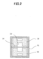
- FIG. 2 is a cross section as viewed from an end surface direction of the device.
- FIG. 3 is a plan view of a circuit board 14 and a metal part 15 placed in the housing of the device.
- the electronic control device has the fundamental structure in which a circuit board 14 having an electronic component 13 thereon is placed in a non-metal (resin) housing having: a housing base 11 integrally comprising via a partition wall 11a a connector inserting section 16 that serves as a male connector used for electrical connection with an external mating connector (female connector) not illustrated; and a housing cover 12 attached to the housing base 11.
- the device houses as a heat sink a pair of elastic metal parts 15 attached to the circuit board 14 at particular positions on its top and bottom surfaces (the positions being located on the side of the partition wall 11a) with the use of a connecting material 17 such as solder or adhesive and supporting the circuit board 14 from the top and bottom sides.
- the device By supporting the top and bottom surfaces of the circuit board 14 with the pair of metal parts 15 in the housing, the device has the function of transferring the heat of the electronic component 13 to the housing and dissipating it to the outside. Also, inside the connector inserting section 16, an edge of the circuit board 14 is inserted into an insertion hole provided in the partition wall 11a, and part of the electric connection pattern on it is exposed.
- the housing base 11 integrally having the connector inserting section 16 and the partition wall 11a is open on the edge side across from the partition wall 11a.
- the housing cover 12 is attached to the opening of the housing base 11 on that edge side.
- the housing cover 12 is preferably formed of resin, but it can also be formed of metal.
- An external mating connector to be used for the connector inserting section 16 is a female card-edge connector to be connected to the terminal of the circuit board 14.
- the pair of the metal parts 15 provided on the top and bottom surfaces (upper and lower positions) of the circuit board 14 are elastic and each have an arch-shaped cross section when viewed from a side surface of the housing base 11.
- the distal ends of the metal parts 15 on the side of the connector inserting section 16 are fixed to the circuit board 14 at particular positions on its top and bottom surfaces with the use of the connecting material 17 such as solder or adhesive.
- the apexes of the arches are in contact with inner wall surfaces of the housing base 11, and the other ends of the metal parts 15 are bent and contacted at a position distanced from the particular positions on the top and bottom surfaces of the circuit board 14 with the mounting position of the electronic component 13 placed therebetween, whereby the circuit board 14 is supported.
- the metal parts 15 support the circuit board 14 at two locations on one side of the circuit board 14 and are supported at a single location on the side of the housing base 11.
- the portions of the metal parts 15 that are located closer to the other portion of the metal parts 15 that are in contact with the circuit board 14 are partially cut off.
- the metal parts 15 have windows at positions corresponding to the terminals of the electronic component 13 on the circuit board 14.
- FIG. 4 is an exploded view of the electronic control device of Embodiment 1, illustrating how its components are assembled.
- FIG. 4 illustrates the assembly method in which when the circuit board 14 having the electronic component 13 thereon is inserted into the housing, the electronic component 13 is mounted on the circuit board 14, the circuit board 14 to which the pair of metal parts 15 are fixed at particular positions on its top and bottom surfaces is then slid inside the housing base 11 to insert an edge of the circuit board 14 into the insertion hole 11b of the partition wall 11a so that part of the circuit board 14 is exposed inside the connector inserting section 16, and the housing cover 12 is then attached to the housing base 11.
- Inner walls of the housing base 11 include guide grooves 11c that support the two lateral edges of the circuit board 14 when the circuit board 14 is slid into the housing base 11.
- the height of the apexes of the convex sections of the metal parts 15 is set larger than that of the opening of the housing base 11 which is the insertion surface for the circuit board 14 (i.e., than the height of the inner wall surfaces of the housing base 11).
- the circuit board 14 when the circuit board 14 is slid into the housing base 11 along the guide grooves 11c on inner wall surfaces of the housing base 11 provided for the circuit board 14 to move it up to the position at which an edge of the circuit board 14 is exposed inside the connector inserting section 16, the convex sections of the pair of metal parts 15 extending from the joint sections of the circuit board 14 on one edge side come into contact with the top and bottom inner wall surfaces of the housing base 11, and the other ends of the metal parts 15 bend inward and come into contact with the top and bottom surfaces of the circuit board 14, thereby supporting the circuit board 14.
- the housing cover 12 By then attaching the housing cover 12 to the opening of the housing base 11, the metal parts 15 are prevented from moving in the circuit board inserting direction, whereby the metal parts 14 can stably support the circuit board 14.
- the housing cover 12 also ensures the sealability (waterproof properties) of the housing.
- FIG. 5 is a side view illustrating another method in which the circuit board 14 and the metal parts 15 to be placed in the housing of the electronic control device of Embodiment 1 are connected by fastening members.
- FIG. 5 illustrates the use of fastening members 18 such screws or bolts in place of the connecting material 17 such as solder or adhesive that connects one end side of the metal parts 15 to the circuit board 14 at particular positions on its top and bottom surfaces.
- the connecting material 17 such as solder or adhesive
- the pair of metal parts 15 connected to the top and bottom surfaces of the circuit board 14 and supporting the circuit board 14 from the top and bottom sides is disposed in the housing, and the function of transferring the heat of the electronic component 13 to the housing to efficiently dissipate it to the outside is obtained by the metal parts 15 supporting the top and bottom surfaces of the circuit board 14 in the housing.
- Embodiment 1 offers a high-grade heat sink that: does not require tight control at the time of manufacturing; does not restrict the range of electronic components that can be used; is structurally simple; can be produced at a higher production rate; is cost-effective; and has sufficient sealability (waterproof properties) It should be noted that the heat sink structure of Embodiment 1 can also be applied to a case where the circuit board 14 is placed upside down in the housing so that the electronic component 13 faces downward.
- FIG. 6 is a cross-sectional side view illustrating the fundamental structure of an electronic control device according to Embodiment 2 of the invention.
- FIG. 7 is a cross section as viewed from an end surface direction of the device.
- the electronic control device of Embodiment 2 differs from that of Embodiment 1 shown in FIG.
- the housing 1 in that it includes as a heat sink a single elastic metal part 15 attached to the circuit board 14 at a particular position on its bottom surface (the position being located on the side of the partition wall 11a) with the use of the connecting material 17 such as solder or adhesive and supporting the circuit board 14 from the bottom side and has the function of transferring the heat of the electronic component 13 to the housing to dissipate it to the outside by the single metal part 15 supporting the bottom surface of the circuit board 14 in the housing.
- the connecting material 17 such as solder or adhesive
- FIG. 8 is an exploded view of the electronic control device of Embodiment 2, illustrating how its components are assembled.
- FIG. 8 illustrates the assembly method in which when the circuit board 14 having the electronic component 13 thereon is inserted into the housing, the electronic component 13 is mounted on the circuit board 14, the circuit board 14 to which the metal part 15 is fixed at a particular position on its bottom surfaces is then slid inside the housing base 11 along the guide grooves 11c to insert an edge of the circuit board 14 into the insertion hole 11b of the partition wall 11a so that part of the circuit board 14 is exposed inside the connector inserting section 16, and the housing cover 12 is then attached to the housing base 11.
- the height of the apex of the convex section of the metal part 15 is set larger than the lower height of the opening of the housing base 11 which is the insertion surface of the circuit board 14 (i.e., than the lower height of inner wall surfaces of the housing base 11).
- the convex section of the metal part 15 extending from the bottom-side joint section of the circuit board 14 on one edge side comes into contact with the bottom inner wall surface of the housing base 11, and the other end of the metal parts 15 bends inward and comes into contact with the bottom surface of the circuit board 14, thereby supporting the circuit board 14.
- the housing cover 12 attaching the housing cover 12 to the opening of the housing base 11, the metal part 15 is prevented from moving in the circuit board inserting direction, whereby the metal part 14 can stably support the circuit board 14.
- the housing cover 12 also ensures the sealability (waterproof properties) of the housing.
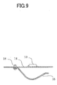
- FIG. 9 is a side view illustrating another method in which the circuit board 14 and the metal part 15 to be placed in the housing of the electronic control device of Embodiment 2 are connected by fastening members.
- FIG. 5 illustrates the use of fastening members 18 such screws or bolts in place of the connecting material 17 such as solder or adhesive that connects one end side of the metal part 15 to the circuit board 14 at a particular position on its bottom surface.
- the connecting material 17 such as solder or adhesive
- the metal part 15 connected to the bottom surface of the circuit board 14 and supporting the circuit board 14 from the bottom side is disposed in the housing, and the function of transferring the heat of the electronic component 13 to the housing to efficiently dissipate it to the outside is obtained by the metal part 15 supporting the bottom surface of the circuit board 14 in the housing.
- the heat sink structure of Embodiment 2 has somewhat lower heat dissipating capabilities than that of Embodiment 1, Embodiment 2 allows the use of a wider range of electronic components than Embodiment 1 since no metal part 15 is present on the top surface of the circuit board 14.
- Embodiment 2 offers a high-grade heat sink that: does not require tight control at the time of manufacturing; is structurally simple; can be produced at a higher production rate; is cost-effective; and has sufficient sealability (waterproof properties).
- the metal part 15 can instead be provided on the top surface of the circuit board 14, or the circuit board 14 can instead be placed upside down in the housing so that the electronic component 13 faces downward.
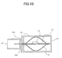
- FIG. 10 is a cross-sectional side view illustrating the fundamental structure of an electronic control device according to Embodiment 3 of the invention.
- the electronic control device of Embodiment 3 differs from that of Embodiment 1 shown in FIG. 1 in that it includes as a heat sink a single elastic metal part 15 having U-shaped bent sections 15a that engage with the edge of the circuit board 14 on the side of the partition wall 11a (the insertion side), the metal part 15 supporting the circuit board 14 from the top and bottom sides, and the device has the function of transferring the heat of the electronic component 13 to the housing to dissipate it to the outside by the single metal part 15 supporting the top and bottom surfaces of the circuit board 14 in the housing.
- FIG. 11 is an exploded view of the electronic control device of Embodiment 3, illustrating how its components are assembled.
- FIG. 11 illustrates the assembly method in which when the circuit board 14 having the electronic component 13 thereon is inserted into the housing, particular positions at the insertion-side edge of the circuit board 14 having the electronic component 13 is brought into contact with and engaged with the bent sections 15a of the metal part 15, the circuit board 14 and the metal part 15 are then slid inside the housing base 11 along the guide grooves 11c, the bent sections 15a and an edge of the circuit board 14 are then inserted into the insertion hole 11b' of the partition wall 11a that has a larger section provided for the bent sections 15a of the metal part 15 so that part of the circuit board 14 is exposed inside the connector inserting section 16, and the housing cover 12 is then attached to the housing base 11.
- the height of the apexes of the convex sections of the metal part 15 is set larger than that of the opening of the housing base 11 which is the insertion surface of the circuit board 14 (i.e., than the height of inner wall surfaces of the housing base 11).
- the circuit board 14 when the circuit board 14 is slid into the housing base 11 along the guide grooves 11c on inner wall surfaces of the housing base 11 that guide the circuit board 14 to move it up to the position at which an edge of the circuit board 14 is exposed inside the connector inserting section 16, the convex sections of the metal part 15 extending from the joint section of the circuit board 14 on one edge side come into contact with the top and bottom inner wall surfaces of the housing base 11, and the other ends of the metal part 15 bend inward and come into contact with the top and bottom surfaces of the circuit board 14, thereby supporting the circuit board 14.
- the housing cover 12 By then attaching the housing cover 12 to the opening of the housing base 11, the metal part 15 is prevented from moving in the circuit board inserting direction, whereby the metal part 14 can stably support the circuit board 14.
- the housing cover 12 also ensures the sealability (waterproof properties) of the housing.
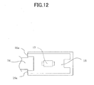
- FIG. 12 is a plan view of the circuit board 14 and the metal part 15 placed in the housing of the device of Embodiment 3. As illustrated in FIG. 12 , the portions of the metal part 15 that are located closer to the other portion of the metal parts 15 that are in contact with the circuit board 14 are partially cut off, as is similar to Embodiment 1 ( FIG. 3 ). However, unlike Embodiment 1, the metal part 15 of Embodiment 3 has no window at positions corresponding to the terminals of the electronic component 13 on the circuit board 14. In addition, unlike Embodiment 1, the top and bottom sides of the metal part 15 of Embodiment 3 are continuous at two locations distanced from each other at the inserting-side edge of the circuit board 14.
- the metal part 15 bent at the bent sections 15a in such a way as to stride across the top and bottom surfaces of the circuit board 14, engaged with an edge of the circuit board 14, and supporting the top and bottom surfaces of the circuit board 14 is disposed in the housing, and the function of transferring the heat of the electronic component 13 to the housing to efficiently dissipate it to the outside is obtained by the metal part 15 simultaneously supporting the top and bottom surfaces of the circuit board 14 in the housing.
- Embodiment 3 does not involve the use of the connecting material 17 nor the fastening members 18 unlike Embodiments 1 and 2, the electronic control device of Embodiment 3 can be produced more easily, at a higher production rate, and at lower costs, without requiring tight control at the time of manufacturing. Also, similar to Embodiment 1, Embodiment 3 results in a high-grade heat sink structure having sufficient sealability (waterproof properties). It should be noted that the heat sink structure of Embodiment 3 can also be applied to a case where the circuit board 14 is placed upside down in the housing so that the electronic component 13 faces downward.
- the metal part 15 of Embodiment 3 can be deformed to prevent its displacement when the circuit board 14 is slid into the housing.
- FIG. 13 is a side view illustrating an example of engaging the metal part 15 with the circuit board 14 by deforming the metal part 15
- FIG. 14 is a plan view illustrating the circuit board 14 and the deformed metal part 15.
- the metal part 15 in addition to the two bent sections 15a distanced from each other at the inserting-side edge of the circuit board 14, the metal part 15 further includes four anti-displacement bent sections 15b extending from the lateral sides of the metal part 15, two of which are bent downward at positions closer to the bent sections 15a, the other two of which are bent upward at positions farther away from the bent sections 15a.
- the four anti-displacement bent sections 15b are positioned such that they come into contact with the lateral sides of the circuit board 14 at different positions. It should be noted that the bending direction can be reversed.
- the anti-displacement bent sections 15b prevent the metal part 15 from moving in lateral directions and in the circuit board inserting direction when the circuit board 14 is slid into the housing, thus ensuring accurate assembly.
- Such anti-displacement bent sections can also be applied to the metal parts of all the embodiments of the invention except Embodiments 5 and 6.
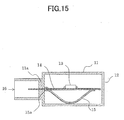
- FIG. 15 is a cross-sectional side view illustrating the fundamental structure of an electronic control device according to Embodiment 4 of the invention.
- the electronic control device of Embodiment 4 differs from that of Embodiment 3 shown in FIG. 10 in that it includes as a heat sink a single elastic metal part 15 having U-shaped bent sections 15a that engage with the edge of the circuit board 14 on the side of the partition wall 11a (the insertion side), the metal part 15 supporting the circuit board 14 from the bottom side, and the device has the function of transferring the heat of the electronic component 13 to the housing to dissipate it to the outside by the single metal part 15 supporting the bottom surface of the circuit board 14 in the housing.
- the single metal part 15 connected at the bent sections 15a in such a way as to stride across the bottom surface of the circuit board 14 and supporting the bottom surface of the circuit board 14 is disposed in the housing, and the function of transferring the heat of the electronic component 13 to the housing to efficiently dissipate it to the outside is obtained by the metal part 15 supporting the bottom surface of the circuit board 14 in the housing.
- the heat sink structure of Embodiment 4 has somewhat lower heat dissipating capabilities than that of Embodiment 3, Embodiment 4 allows the use of a wider range of electronic components than Embodiment 3 since no metal part is present on the top surface of the circuit board 14.
- Embodiment 4 does not involve the use of the connecting material 17 nor the fastening members 18 unlike Embodiments 1 and 2, the electronic control device of Embodiment 3 can be produced more easily, at a higher production rate, and at lower costs without requiring tight control at the time of manufacturing and can achieve sufficient sealability (waterproof properties).
- the metal part 15 can instead be provided on the top surface of the circuit board 14, or the circuit board 14 can instead be placed upside down in the housing so that the electronic component 13 faces downward.
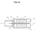
- FIG. 16 is a cross-sectional side view illustrating the fundamental structure of an electronic control device according to Embodiment 5 of the invention.
- FIG. 17 is a cross section as viewed from an end surface direction of the device.
- the device of Embodiment 5 differs from that of Embodiment 1 in that it includes as a heat sink a metal part 15 that is slid into the housing base 11 with the metal part 15 sandwiching the lateral edges of the top and bottom surfaces of the circuit board 14, and the metal part 15 is elastic, has an arch-shaped cross section as viewed from an end surface direction of the housing base 11, extends also in a side surface direction of the housing base 11, and has bent sections 15a at two locations distanced from each other at the insertion-side edge of the circuit board.
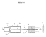
- FIG. 18 is an exploded view of the electronic control device of Embodiment 5, illustrating how its components are assembled.
- FIG. 18 illustrates the assembly method in which when the circuit board 14 on which the electronic component 13 is mounted is inserted into the housing, the circuit board 14 on which the electronic component 13 is mounted is inserted into the space of the metal part 15, particular positions at the insertion-side edge of the circuit board 14 are then brought into contact with and engaged with the bent sections 15a of the metal part 15, the circuit board 14 and the metal part 15 are then slid inside the housing base 11 along the guide grooves 11c, the bent sections 15a and an edge of the circuit board 14 are then inserted into the insertion hole 11b' of the partition wall 11a that has a larger section provided for the bent sections 15a of the metal part 15 so that part of the circuit board 14 is exposed inside the connector inserting section 16, and the housing cover 12 is then attached to the housing base 11.
- the height of the apexes of the convex sections of the metal part 15 is set larger than that of the opening of the housing base 11 which is the insertion surface of the circuit board 14 (i.e., than the height of inner wall surfaces of the housing base 11).
- the circuit board 14 and the metal part 15 are slid along the guide grooves 11c on inner wall surfaces of the housing base 11 that guide the circuit board 14 to move it up to the position at which an edge of the circuit board 14 is exposed inside the connector inserting section 16, the convex sections of the metal part 15 come into contact with the top and bottom inner wall surfaces of the housing base 11, and the other ends of the metal part 15 bend slightly inward and come into contact with the top and bottom surfaces of the circuit board 14, thereby being supported by inner side walls of the housing base 11.
- the housing cover 12 By then attaching the housing cover 12 to the opening of the housing base 11, the metal part 15 is prevented from moving in the circuit board inserting direction, whereby the metal part 15 can stably support the circuit board 14.
- the housing cover 12 also ensures the sealability (waterproof properties) of the housing.
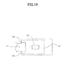
- FIG. 19 is a plan view of the circuit board 14 and the metal part 15 placed in the housing of the device of Embodiment 5. As illustrated in FIG. 19 , the portions of the metal part 15 that are located closer to the partition wall 11a are partially cut off, as is similar to the metal parts 15 of Embodiment 1 shown in FIG. 3 . However, unlike Embodiment 1, the metal part 15 of Embodiment 3 has no window at positions corresponding to the terminals of the electronic component 13 on the circuit board 14, and the circuit board 14 is inserted into the space created at the two mutually distant bent sections 15a with which the inserting-side edge of the circuit board 14 is brought into contact.
- the single metal part 15 sandwiching the lateral edges of the top and bottom surfaces of the circuit board 14, bent at the bent sections 15a in such a way as to stride across the top and bottom surfaces of the circuit board 14, engaged with an edge of the circuit board 14, and supporting the circuit board 14 from the top and bottom sides is disposed in the housing, and the function of transferring the heat of the electronic component 13 to the housing to efficiently dissipate it to the outside is obtained by the metal parts 15 simultaneously supporting the top and bottom surfaces of the circuit board 14 in the housing.
- Embodiment 5 does not involve the use of the connecting material 17 nor the fastening members 18 similar to Embodiment 3, the electronic control device of Embodiment 5 can be produced more easily, at a higher production rate, and at lower costs, without requiring tight control at the time of manufacturing. Also, similar to Embodiment 1, Embodiment 5 results in a high-grade heat sink structure having sufficient sealability (waterproof properties). It should be noted that the heat sink structure of Embodiment 5 can also be applied to a case where the circuit board 14 is placed upside down in the housing so that the electronic component 13 faces downward.
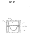
- FIG. 20 is a cross section as viewed from an end surface direction of an electronic control device according to Embodiment 6 of the invention.
- the electronic control device of Embodiment 6 differs from the structure of Embodiment 5 shown in FIGS. 16 through 19 in that it includes as a heat sink a metal part 15, both edges of which are deformed into concave and convex shapes and are elastic with respect to the guide grooves 11c inside the housing base 11 along which the circuit board 14 is slid, in that the metal part 15 has no bent sections 15a, and in that the metal part 15 is provided on the bottom side of the circuit board 14.
- the metal part 15 pressure-bonded to the side-directional bottom surface edge of the circuit board 14 within the guide grooves 11c and supporting the bottom surface of the circuit board 14 is disposed in the housing, and the function of transferring the heat of the electronic component 13 to the housing to efficiently dissipate it to the outside is obtained by the metal part 15 supporting the bottom surface of the circuit board 14 in the housing.
- the heat sink structure of Embodiment 6 has somewhat lower heat dissipating capabilities than that of Embodiment 5, Embodiment 6 allows the use of a wider range of electronic components than Embodiment 5 since no metal part 15 is present on the top surface of the circuit board 14.
- Embodiment 6 offers a high-grade heat sink that: does not require tight control at the time of manufacturing; is structurally simple; can be produced at a higher production rate; is cost-effective; and has sufficient sealability (waterproof properties).
- the metal part 15 can instead be provided on the top surface of the circuit board 14, or the circuit board 14 can instead be placed upside down in the housing so that the electronic component 13 faces downward.
- FIG. 21 is a cross-sectional side view illustrating the fundamental structure of an electronic control device according to Embodiment 7 of the invention.
- the device of Embodiment 7 differs from that of Embodiment 2 shown in FIG. 6 in that it includes as a heat sink a heat sink piece 15c provided by local cutting in a single metal part 15 provided on the bottom side of the circuit board 14 within the housing and coming into contact with the position corresponding to the mounting part of the electronic component 13 (located closer to the partition wall 11a than in FIG.
- the heat sink piece 15c is located close to the inserting section of the circuit board 14, the influence of deformation amount variations according to the bending amount of the metal part 15 is small when the circuit board 14 is slid into the housing base 11 after the heat sink piece 15c is attached to the circuit board 14.
- the single metal part 15 disposed in the housing, connected to the bottom surface of the circuit board 14, and supporting the circuit board 14 from the bottom surface is provided with the heat sink piece 15c coming into contact with the corresponding position on the bottom surface of the circuit board 14 at which the electronic component 13 is mounted, and the function of transferring the heat of electronic component 13 from the corresponding position on bottom surface of the circuit board 14 through the heat sink piece 15c and the main body of the metal part 15 to the housing to efficiently dissipate it to the outside is obtained by the metal part 15 supporting the bottom surface of the circuit board 14 in the housing.
- the heat sink structure of Embodiment 7 has higher heat dissipating capabilities than that of Embodiment 2 shown in FIG.
- Embodiment 7 offers a high-grade heat sink that: does not require tight control at the time of manufacturing; is structurally simple; can be produced at a higher production rate; is cost-effective; and has sufficient sealability (waterproof properties).
- FIG. 22 is a cross-sectional side view illustrating the fundamental structure of an electronic control device according to Embodiment 8 of the invention.
- the device of Embodiment 8 differs from that of Embodiment 7 shown in FIG. 21 in that it adopts the structure in which the circuit board 14 is placed upside down in the housing so that the electronic component 13 faces downward and has the function of directly transferring the heat of the electronic component 13 from the heat sink piece 15c itself through the main body of the metal part 15 to the housing to dissipate it to the outside by allowing the heat sink piece 15c to directly touch the electronic component 13 on the surface side of the circuit board 14.
- the single metal part 15 disposed in the housing, connected to a surface of the circuit board 14, and supporting the surface of the circuit board 14 is provided with the heat sink piece 15c that directly touches the electronic component 13 themselves on the surface of the circuit board 14, and the function of transferring the heat of electronic component 13 from the heat sink piece 15c itself through the main body of the metal part 15 to the housing to efficiently dissipate it to the outside is obtained by the metal part 15 supporting the surface of the circuit board 14 in the housing.
- Embodiment 8 has higher heat dissipating capabilities than that of Embodiment 7 and also allows the use of a wider range of electronic components than Embodiment 7 since no metal part 15 is present on the top surface of the circuit board 14.
- Embodiment 8 offers a high-grade heat sink that: does not require tight control at the time of manufacturing; is structurally simple; can be produced at a higher production rate; is cost-effective; and has sufficient sealability (waterproof properties).
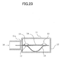
- FIG. 23 is a cross-sectional side view illustrating the fundamental structure of an electronic control device according to Embodiment 9 of the invention.
- the device of Embodiment 9 differs from that of Embodiment 2 shown in FIG. 6 in that two electronic components 13 are mounted on both sides on the top surface of the circuit board 14 in a lateral direction, and among the two positions on the bottom surface of the circuit board 14 corresponding to the mounting positions of the electronic components 13, one end of a metal part 15 is connected to the position on the side of the partition wall 11a with the use of the connecting material such as solder or adhesive, and the other end of the metal part 15 is bent and brought into contact with the other position on the side of the housing cover 12 when the circuit board 14 is slid into the housing base 11.
- the metal part 15 connected to the bottom surface of the circuit board 14 and supporting the bottom surface of the circuit board 14 is disposed in the housing, and the function of transferring the heat of the electronic components 13 from the both end sides of the metal part 15 that touch the positions corresponding to the mounting positions through the main body of the metal part 15 to the housing to efficiently dissipate it to the outside is obtained by the metal part 15 supporting the bottom surface of the circuit board 14 in the housing.
- the heat sink structure of Embodiment 9 has heat dissipating capabilities similar to that of Embodiment 2 and also allows the use of a wider range of electronic components than Embodiment 2 since no metal part 15 is present on the top surface of the circuit board 14.
- Embodiment 9 offers a high-grade heat sink that: does not require tight control at the time of manufacturing; is structurally simple; can be produced at a higher production rate; is cost-effective; and has sufficient sealability (waterproof properties).
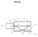
- FIG. 24 is a cross-sectional side view illustrating the fundamental structure of an electronic control device according to Embodiment 10 of the invention.
- the device of Embodiment 10 differs from that of Embodiment 9 shown in FIG. 23 in that a single electronic component 13 is mounted on the top surface of the circuit board 14 at a position on the side of the housing cover 12 in a lateral direction, one end of a single metal part 15 is connected to a position on the bottom surface of the circuit board 14 on the side of the partition wall 11a with the use of the connecting material 17 such as solder or adhesive, and the other end of the metal part 15 is bent and brought into contact with the position corresponding to the mounting position of the electronic component 13 on the side of the housing cover 12 when the circuit board 14 is slid into the housing 11, in that a wall surface of the housing base 11 in a lateral direction is partially open so that an external convex-shaped metal part 20 used for heat dissipation is attached, and in that as to the external metal part 20, its apex touches the
- the single metal part 15 connected to the bottom surface of the circuit board 14 and supporting the bottom surface of the circuit board 14 is disposed in the housing, the external metal part 20 is attached to the opening on a side surface of the housing, the metal part 15 supports the bottom surface of the circuit board 14 in the housing, the apex of the external metal part 20 supports the apex of the metal part 15, and the function of transferring the heat of the electronic component 13 from the other end of the metal part 15 connected to the position corresponding to the mounting position of the electronic component 13 through the main body of the metal part 15 to the external metal part 20 to efficiently dissipate it to the outside is obtained.
- Embodiment 10 has higher heat dissipating capabilities than those of the previous embodiments and also allows the use of a wider range of electronic components since no metal part 15 is present on the top surface of the circuit board 14.
- Embodiment 10 offers a high-grade heat sink that: does not require tight control at the time of manufacturing; is structurally simple; can be produced at a higher production rate; and is cost-effective. Also, since the external metal part 20 is attached to the housing base 11 with the filler material 19 for sealing placed therebetween, a high-grade heat sink structure having sufficient sealability (waterproof properties) can be obtained.
- the heat sink structure of Embodiment 10 can be changed to the structure in which a metal part 15 is disposed also on the top surface of the circuit board 14 as in Embodiment 1 described with reference to FIGS. 1 through 5 and the other end of the metal part 15 directly touches the electronic component 13.
- the heat sink structure of Embodiment 1 can also be applied to a case where the circuit board 14 is placed upside down in the housing so that the electronic component 13 faces downward.
- FIG. 25 is a cross-sectional side view illustrating the fundamental structure of an electronic control device according to Embodiment 11 of the invention.
- the device of Embodiment 11 differs from that of Embodiment 10 shown in FIG. 24 in that an external convex-shaped metal part 20' has a section with which to fix the housing base 11 and the metal part 20' itself with the use of fastening members.
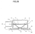
- FIG. 26 is a cross-sectional side view illustrating the fundamental structure of an electronic control device according to Embodiment 12 of the invention.
- the device of Embodiment 12 differs from that of Embodiment 10 shown in FIG. 24 in that two electronic components 13 are mounted on both sides on the top surface of the circuit board 14 in a lateral direction, and an external metal part 20" is fixed by fastening members to an external member after the external convex-shaped metal part 20" is attached to the opening of the housing base 11.
Landscapes
- Engineering & Computer Science (AREA)
- Microelectronics & Electronic Packaging (AREA)
- Physics & Mathematics (AREA)
- Thermal Sciences (AREA)
- Cooling Or The Like Of Electrical Apparatus (AREA)
- Casings For Electric Apparatus (AREA)
- Mounting Of Printed Circuit Boards And The Like (AREA)
Abstract
Description
- The present invention relates to an electronic control device having a heat sink for efficiently dissipating heat from the electronic component mounted on the circuit board housed in the device.
- Conventionally, an example of known techniques related to the heat sink structure applied to electronic control devices of this kind is "heat sink structure for electronic components" (see Patent Document 1) in which the lower end of a strip-shaped metal plate having spring properties is fixed to a printed board, the upper end of the metal plate is pressed onto the ceiling of the housing to which to insert the printed board, an electronic component to be mounted on the printed board is attached to the metal plate, the upper end of the metal plate is bent into the shape of '<' in vertical cross section, and one piece of the metal plate on its distal end is in contact with the ceiling of the housing.
- Another known technique related to similar heat sink structures is "vehicle-mounted electronic device" (see Patent Document 2) in which multiple printed circuit boards having a particular shape on which electronic components are mounted with a metal plate having a particular shape placed therebetween is attached, these printed circuit boards are electrically connected to each other by external connecting means to form a laminate structure, a connector is connected to one edge of the laminate structure, and all the portion except the front surface of the connector and a particular portion of the metal plate is resin-sealed.
-
- Patent Document 1:
JP-2011-54895-A - Patent Document 2:
JP-1997-27688-A - According to the technique of
Patent Document 1, the printed circuit board having an electronic component thereon is fixed to one side of the housing that covers it, the upper end of the metal plate is pressed onto the ceiling of the housing, the lower end of the metal plate is fixed to the printed board, and the top surface of the electronic component is disposed vertically with respect to the printed circuit board. Thus, in order that the metal plate is prevented from being displaced due to the influence of horizontal (lateral) displacement on the printed circuit board, a fixing structure for fixing the printed circuit board and the housing is necessary, complicating the structure of the device. This results in a cost increase and lower productivity. In addition, the application of the electronic component is restricted by the range of the size of the metal plate attachment section in the back height direction of the housing. - In the technique of Patent Document 2, the printed circuit boards on which electronic components are mounted with the metal plate placed therebetween are connected by external flexible connecting means, and the entire portion is resin-sealed. Thus, tight standards control is necessary to ensure the reliability of the basic operation of the electronic components and the connection of the printed circuit boards at the time of manufacturing, and temperature and time need to be controlled tightly in the manufacturing environment to perform quality control. This results in a cost increase and lower productivity.
- The present invention has been made to solve the above problems, and its object is to provide an electronic control device having a high-grade heat sink that: does not require tight control at the time of manufacturing; does not restrict the range of electronic components that can be used; is structurally simple; can be produced at a higher production rate; and is cost-effective.
- To solve the above problems, the invention provides an electronic control device in which a circuit board having an electronic component thereon is mounted in a housing integrally having via a partition wall a connector inserting section used for electrical connection with an external mating connector, wherein part of the circuit board being exposed within the connector inserting section by being inserted into an insertion hole provided in the partition wall, the electronic control device comprising an elastic metal part disposed in the housing, the elastic metal part being connected to a particular position on the circuit board and supporting the circuit board.
- In the electronic control device of the invention, because the metal part connected to and supporting the circuit board is disposed in the housing and the device has the function of transferring the heat of the electronic component to the housing to efficiently dissipate it to the outside by the metal part supporting the circuit board in the housing, the invention offers a high-grade heat sink that: does not require tight control at the time of manufacturing; does not restrict the range of electronic components that can be used; is structurally simple; can be produced at a higher production rate; and is cost-effective.
-
-
FIG. 1 is a cross-sectional side view illustrating the fundamental structure of an electronic control device according toEmbodiment 1 of the invention; -
FIG. 2 is a cross section as viewed from an end surface direction of the device ofFIG. 1 ; -
FIG. 3 is a plan view of a circuit board and a metal part placed in the housing of the device ofFIG. 1 ; -
FIG. 4 is an exploded view of the electronic control device ofFIG. 1 , illustrating how its components are assembled; -
FIG. 5 is a side view illustrating another method in which the circuit board and the metal parts to be placed in the housing of the electronic control device ofFIG. 1 are connected by fastening members; -
FIG. 6 is a cross-sectional side view illustrating the fundamental structure of an electronic control device according to Embodiment 2 of the invention; -
FIG. 7 is a cross section as viewed from an end surface direction of the device ofFIG. 6 ; -
FIG. 8 is an exploded view of the electronic control device ofFIG. 6 , illustrating how its components are assembled; -
FIG. 9 is a side view illustrating another method in which the circuit board and the metal part to be placed in the housing of the electronic control device ofFIG. 6 are connected by fastening members; -
FIG. 10 is a cross-sectional side view illustrating the fundamental structure of an electronic control device according to Embodiment 3 of the invention; -
FIG. 11 is an exploded view of the electronic control device ofFIG. 10 , illustrating how its components are assembled; -
FIG. 12 is a plan view of a circuit board and a metal part placed in the housing of the device ofFIG. 10 ; -
FIG. 13 is a side view illustrating an example of engaging the metal part ofFIG. 10 with the circuit board by deforming the metal part; -
FIG. 14 is a plan view of the circuit board and the metal part shown inFIG. 13 ; -
FIG. 15 is a cross-sectional side view illustrating the fundamental structure of an electronic control device according to Embodiment 4 of the invention; -
FIG. 16 is a cross-sectional side view illustrating the fundamental structure of an electronic control device according to Embodiment 5 of the invention; -
FIG. 17 is a cross section as viewed from an end surface direction of the device ofFIG. 16 ; -
FIG. 18 is an exploded view of the electronic control device ofFIG. 16 , illustrating how its components are assembled; -
FIG. 19 is a plan view of a circuit board and a metal part placed in the housing of the device ofFIG. 16 ; -
FIG. 20 is a cross section as viewed from an end surface direction of an electronic control device according to Embodiment 6 of the invention; -
FIG. 21 is a cross-sectional side view illustrating the fundamental structure of an electronic control device according to Embodiment 7 of the invention; -
FIG. 22 is a cross-sectional side view illustrating the fundamental structure of an electronic control device according to Embodiment 8 of the invention; -
FIG. 23 is a cross-sectional side view illustrating the fundamental structure of an electronic control device according to Embodiment 9 of the invention; -
FIG. 24 is a cross-sectional side view illustrating the fundamental structure of an electronic control device according to Embodiment 10 of the invention; -
FIG. 25 is a cross-sectional side view illustrating the fundamental structure of an electronic control device according toEmbodiment 11 of the invention; and -
FIG. 26 is a cross-sectional side view illustrating the fundamental structure of an electronic control device according toEmbodiment 12 of the invention. - Electronic control devices according to embodiments of the invention will now be described with reference to the accompanying drawings.
-
FIG. 1 is a cross-sectional side view illustrating the fundamental structure of an electronic control device according toEmbodiment 1 of the invention.FIG. 2 is a cross section as viewed from an end surface direction of the device.FIG. 3 is a plan view of acircuit board 14 and ametal part 15 placed in the housing of the device. - The electronic control device has the fundamental structure in which a
circuit board 14 having anelectronic component 13 thereon is placed in a non-metal (resin) housing having: ahousing base 11 integrally comprising via apartition wall 11a aconnector inserting section 16 that serves as a male connector used for electrical connection with an external mating connector (female connector) not illustrated; and ahousing cover 12 attached to thehousing base 11. In addition, the device houses as a heat sink a pair ofelastic metal parts 15 attached to thecircuit board 14 at particular positions on its top and bottom surfaces (the positions being located on the side of thepartition wall 11a) with the use of a connectingmaterial 17 such as solder or adhesive and supporting thecircuit board 14 from the top and bottom sides. By supporting the top and bottom surfaces of thecircuit board 14 with the pair ofmetal parts 15 in the housing, the device has the function of transferring the heat of theelectronic component 13 to the housing and dissipating it to the outside. Also, inside theconnector inserting section 16, an edge of thecircuit board 14 is inserted into an insertion hole provided in thepartition wall 11a, and part of the electric connection pattern on it is exposed. - Among these components, the
housing base 11 integrally having theconnector inserting section 16 and thepartition wall 11a is open on the edge side across from thepartition wall 11a. Thehousing cover 12 is attached to the opening of thehousing base 11 on that edge side. Thehousing cover 12 is preferably formed of resin, but it can also be formed of metal. An external mating connector to be used for theconnector inserting section 16 is a female card-edge connector to be connected to the terminal of thecircuit board 14. The pair of themetal parts 15 provided on the top and bottom surfaces (upper and lower positions) of thecircuit board 14 are elastic and each have an arch-shaped cross section when viewed from a side surface of thehousing base 11. The distal ends of themetal parts 15 on the side of theconnector inserting section 16 are fixed to thecircuit board 14 at particular positions on its top and bottom surfaces with the use of the connectingmaterial 17 such as solder or adhesive. The apexes of the arches are in contact with inner wall surfaces of thehousing base 11, and the other ends of themetal parts 15 are bent and contacted at a position distanced from the particular positions on the top and bottom surfaces of thecircuit board 14 with the mounting position of theelectronic component 13 placed therebetween, whereby thecircuit board 14 is supported. In this state, themetal parts 15 support thecircuit board 14 at two locations on one side of thecircuit board 14 and are supported at a single location on the side of thehousing base 11. In addition, as illustrated inFIGS. 2 and3 , the portions of themetal parts 15 that are located closer to the other portion of themetal parts 15 that are in contact with thecircuit board 14 are partially cut off. In addition, themetal parts 15 have windows at positions corresponding to the terminals of theelectronic component 13 on thecircuit board 14. -
FIG. 4 is an exploded view of the electronic control device ofEmbodiment 1, illustrating how its components are assembled.FIG. 4 illustrates the assembly method in which when thecircuit board 14 having theelectronic component 13 thereon is inserted into the housing, theelectronic component 13 is mounted on thecircuit board 14, thecircuit board 14 to which the pair ofmetal parts 15 are fixed at particular positions on its top and bottom surfaces is then slid inside thehousing base 11 to insert an edge of thecircuit board 14 into theinsertion hole 11b of thepartition wall 11a so that part of thecircuit board 14 is exposed inside theconnector inserting section 16, and thehousing cover 12 is then attached to thehousing base 11. Inner walls of thehousing base 11 includeguide grooves 11c that support the two lateral edges of thecircuit board 14 when thecircuit board 14 is slid into thehousing base 11. Further, the height of the apexes of the convex sections of themetal parts 15 is set larger than that of the opening of thehousing base 11 which is the insertion surface for the circuit board 14 (i.e., than the height of the inner wall surfaces of the housing base 11). Accordingly, when thecircuit board 14 is slid into thehousing base 11 along theguide grooves 11c on inner wall surfaces of thehousing base 11 provided for thecircuit board 14 to move it up to the position at which an edge of thecircuit board 14 is exposed inside theconnector inserting section 16, the convex sections of the pair ofmetal parts 15 extending from the joint sections of thecircuit board 14 on one edge side come into contact with the top and bottom inner wall surfaces of thehousing base 11, and the other ends of themetal parts 15 bend inward and come into contact with the top and bottom surfaces of thecircuit board 14, thereby supporting thecircuit board 14. By then attaching thehousing cover 12 to the opening of thehousing base 11, themetal parts 15 are prevented from moving in the circuit board inserting direction, whereby themetal parts 14 can stably support thecircuit board 14. Thehousing cover 12 also ensures the sealability (waterproof properties) of the housing. -
FIG. 5 is a side view illustrating another method in which thecircuit board 14 and themetal parts 15 to be placed in the housing of the electronic control device ofEmbodiment 1 are connected by fastening members.FIG. 5 illustrates the use offastening members 18 such screws or bolts in place of the connectingmaterial 17 such as solder or adhesive that connects one end side of themetal parts 15 to thecircuit board 14 at particular positions on its top and bottom surfaces. In such a case, after one end side of the pair of themetal parts 15 in which holes are punched is brought into contact with and aligned with holes at particular positions on the top and bottom surfaces of thecircuit board 14 in such a way as to sandwich thecircuit board 14, they can be fastened together with thefastening members 18. That is, in the electronic control device ofEmbodiment 1, either the connectingmaterial 17 or thefastening members 18 can be used to connect themetal parts 15 to thecircuit board 14. - In the heat sink structure of the electronic control device of
Embodiment 1, the pair ofmetal parts 15 connected to the top and bottom surfaces of thecircuit board 14 and supporting thecircuit board 14 from the top and bottom sides is disposed in the housing, and the function of transferring the heat of theelectronic component 13 to the housing to efficiently dissipate it to the outside is obtained by themetal parts 15 supporting the top and bottom surfaces of thecircuit board 14 in the housing. Thus,Embodiment 1 offers a high-grade heat sink that: does not require tight control at the time of manufacturing; does not restrict the range of electronic components that can be used; is structurally simple; can be produced at a higher production rate; is cost-effective; and has sufficient sealability (waterproof properties) It should be noted that the heat sink structure ofEmbodiment 1 can also be applied to a case where thecircuit board 14 is placed upside down in the housing so that theelectronic component 13 faces downward. -
FIG. 6 is a cross-sectional side view illustrating the fundamental structure of an electronic control device according to Embodiment 2 of the invention.FIG. 7 is a cross section as viewed from an end surface direction of the device. The electronic control device of Embodiment 2 differs from that ofEmbodiment 1 shown inFIG. 1 in that it includes as a heat sink a singleelastic metal part 15 attached to thecircuit board 14 at a particular position on its bottom surface (the position being located on the side of thepartition wall 11a) with the use of the connectingmaterial 17 such as solder or adhesive and supporting thecircuit board 14 from the bottom side and has the function of transferring the heat of theelectronic component 13 to the housing to dissipate it to the outside by thesingle metal part 15 supporting the bottom surface of thecircuit board 14 in the housing. -
FIG. 8 is an exploded view of the electronic control device of Embodiment 2, illustrating how its components are assembled.FIG. 8 illustrates the assembly method in which when thecircuit board 14 having theelectronic component 13 thereon is inserted into the housing, theelectronic component 13 is mounted on thecircuit board 14, thecircuit board 14 to which themetal part 15 is fixed at a particular position on its bottom surfaces is then slid inside thehousing base 11 along theguide grooves 11c to insert an edge of thecircuit board 14 into theinsertion hole 11b of thepartition wall 11a so that part of thecircuit board 14 is exposed inside theconnector inserting section 16, and thehousing cover 12 is then attached to thehousing base 11. In this embodiment as well, the height of the apex of the convex section of themetal part 15 is set larger than the lower height of the opening of thehousing base 11 which is the insertion surface of the circuit board 14 (i.e., than the lower height of inner wall surfaces of the housing base 11). Accordingly, when thecircuit board 14 is slid into thehousing base 11 along theguide grooves 11c to move it up to the position at which an edge of thecircuit board 14 is exposed inside theconnector inserting section 16, the convex section of themetal part 15 extending from the bottom-side joint section of thecircuit board 14 on one edge side comes into contact with the bottom inner wall surface of thehousing base 11, and the other end of themetal parts 15 bends inward and comes into contact with the bottom surface of thecircuit board 14, thereby supporting thecircuit board 14. By then attaching thehousing cover 12 to the opening of thehousing base 11, themetal part 15 is prevented from moving in the circuit board inserting direction, whereby themetal part 14 can stably support thecircuit board 14. Thehousing cover 12 also ensures the sealability (waterproof properties) of the housing. -
FIG. 9 is a side view illustrating another method in which thecircuit board 14 and themetal part 15 to be placed in the housing of the electronic control device of Embodiment 2 are connected by fastening members.FIG. 5 illustrates the use offastening members 18 such screws or bolts in place of the connectingmaterial 17 such as solder or adhesive that connects one end side of themetal part 15 to thecircuit board 14 at a particular position on its bottom surface. In such a case, after one end side of themetal part 15 in which holes are punched is brought into contact with and aligned with holes at particular positions on the bottom surface of thecircuit board 14, they can be fastened together with thefastening members 18. That is, in the electronic control device of Embodiment 2, too, either the connectingmaterial 17 or thefastening members 18 can be used to connect themetal part 15 to thecircuit board 14. - In the heat sink structure of the electronic control device of Embodiment 2, the
metal part 15 connected to the bottom surface of thecircuit board 14 and supporting thecircuit board 14 from the bottom side is disposed in the housing, and the function of transferring the heat of theelectronic component 13 to the housing to efficiently dissipate it to the outside is obtained by themetal part 15 supporting the bottom surface of thecircuit board 14 in the housing. Although the heat sink structure of Embodiment 2 has somewhat lower heat dissipating capabilities than that ofEmbodiment 1, Embodiment 2 allows the use of a wider range of electronic components thanEmbodiment 1 since nometal part 15 is present on the top surface of thecircuit board 14. In addition, similar toEmbodiment 1, Embodiment 2 offers a high-grade heat sink that: does not require tight control at the time of manufacturing; is structurally simple; can be produced at a higher production rate; is cost-effective; and has sufficient sealability (waterproof properties). It should be noted that in the heat sink structure of Embodiment 2, themetal part 15 can instead be provided on the top surface of thecircuit board 14, or thecircuit board 14 can instead be placed upside down in the housing so that theelectronic component 13 faces downward. -
FIG. 10 is a cross-sectional side view illustrating the fundamental structure of an electronic control device according to Embodiment 3 of the invention. The electronic control device of Embodiment 3 differs from that ofEmbodiment 1 shown inFIG. 1 in that it includes as a heat sink a singleelastic metal part 15 having U-shapedbent sections 15a that engage with the edge of thecircuit board 14 on the side of thepartition wall 11a (the insertion side), themetal part 15 supporting thecircuit board 14 from the top and bottom sides, and the device has the function of transferring the heat of theelectronic component 13 to the housing to dissipate it to the outside by thesingle metal part 15 supporting the top and bottom surfaces of thecircuit board 14 in the housing. -
FIG. 11 is an exploded view of the electronic control device of Embodiment 3, illustrating how its components are assembled.FIG. 11 illustrates the assembly method in which when thecircuit board 14 having theelectronic component 13 thereon is inserted into the housing, particular positions at the insertion-side edge of thecircuit board 14 having theelectronic component 13 is brought into contact with and engaged with thebent sections 15a of themetal part 15, thecircuit board 14 and themetal part 15 are then slid inside thehousing base 11 along theguide grooves 11c, thebent sections 15a and an edge of thecircuit board 14 are then inserted into theinsertion hole 11b' of thepartition wall 11a that has a larger section provided for thebent sections 15a of themetal part 15 so that part of thecircuit board 14 is exposed inside theconnector inserting section 16, and thehousing cover 12 is then attached to thehousing base 11. In this embodiment as well, the height of the apexes of the convex sections of themetal part 15 is set larger than that of the opening of thehousing base 11 which is the insertion surface of the circuit board 14 (i.e., than the height of inner wall surfaces of the housing base 11). Accordingly, when thecircuit board 14 is slid into thehousing base 11 along theguide grooves 11c on inner wall surfaces of thehousing base 11 that guide thecircuit board 14 to move it up to the position at which an edge of thecircuit board 14 is exposed inside theconnector inserting section 16, the convex sections of themetal part 15 extending from the joint section of thecircuit board 14 on one edge side come into contact with the top and bottom inner wall surfaces of thehousing base 11, and the other ends of themetal part 15 bend inward and come into contact with the top and bottom surfaces of thecircuit board 14, thereby supporting thecircuit board 14. By then attaching thehousing cover 12 to the opening of thehousing base 11, themetal part 15 is prevented from moving in the circuit board inserting direction, whereby themetal part 14 can stably support thecircuit board 14. Thehousing cover 12 also ensures the sealability (waterproof properties) of the housing. -
FIG. 12 is a plan view of thecircuit board 14 and themetal part 15 placed in the housing of the device of Embodiment 3. As illustrated inFIG. 12 , the portions of themetal part 15 that are located closer to the other portion of themetal parts 15 that are in contact with thecircuit board 14 are partially cut off, as is similar to Embodiment 1 (FIG. 3 ). However, unlikeEmbodiment 1, themetal part 15 of Embodiment 3 has no window at positions corresponding to the terminals of theelectronic component 13 on thecircuit board 14. In addition, unlikeEmbodiment 1, the top and bottom sides of themetal part 15 of Embodiment 3 are continuous at two locations distanced from each other at the inserting-side edge of thecircuit board 14. - In the heat sink structure of the electronic control device of Embodiment 3, the
metal part 15 bent at thebent sections 15a in such a way as to stride across the top and bottom surfaces of thecircuit board 14, engaged with an edge of thecircuit board 14, and supporting the top and bottom surfaces of thecircuit board 14 is disposed in the housing, and the function of transferring the heat of theelectronic component 13 to the housing to efficiently dissipate it to the outside is obtained by themetal part 15 simultaneously supporting the top and bottom surfaces of thecircuit board 14 in the housing. Since Embodiment 3 does not involve the use of the connectingmaterial 17 nor thefastening members 18 unlikeEmbodiments 1 and 2, the electronic control device of Embodiment 3 can be produced more easily, at a higher production rate, and at lower costs, without requiring tight control at the time of manufacturing. Also, similar toEmbodiment 1, Embodiment 3 results in a high-grade heat sink structure having sufficient sealability (waterproof properties). It should be noted that the heat sink structure of Embodiment 3 can also be applied to a case where thecircuit board 14 is placed upside down in the housing so that theelectronic component 13 faces downward. - The
metal part 15 of Embodiment 3 can be deformed to prevent its displacement when thecircuit board 14 is slid into the housing.FIG. 13 is a side view illustrating an example of engaging themetal part 15 with thecircuit board 14 by deforming themetal part 15 whileFIG. 14 is a plan view illustrating thecircuit board 14 and thedeformed metal part 15. As illustrated, in addition to the twobent sections 15a distanced from each other at the inserting-side edge of thecircuit board 14, themetal part 15 further includes four anti-displacementbent sections 15b extending from the lateral sides of themetal part 15, two of which are bent downward at positions closer to thebent sections 15a, the other two of which are bent upward at positions farther away from thebent sections 15a. The four anti-displacementbent sections 15b are positioned such that they come into contact with the lateral sides of thecircuit board 14 at different positions. It should be noted that the bending direction can be reversed. The anti-displacementbent sections 15b prevent themetal part 15 from moving in lateral directions and in the circuit board inserting direction when thecircuit board 14 is slid into the housing, thus ensuring accurate assembly. Such anti-displacement bent sections can also be applied to the metal parts of all the embodiments of the invention except Embodiments 5 and 6. -
FIG. 15 is a cross-sectional side view illustrating the fundamental structure of an electronic control device according to Embodiment 4 of the invention. The electronic control device of Embodiment 4 differs from that of Embodiment 3 shown inFIG. 10 in that it includes as a heat sink a singleelastic metal part 15 having U-shapedbent sections 15a that engage with the edge of thecircuit board 14 on the side of thepartition wall 11a (the insertion side), themetal part 15 supporting thecircuit board 14 from the bottom side, and the device has the function of transferring the heat of theelectronic component 13 to the housing to dissipate it to the outside by thesingle metal part 15 supporting the bottom surface of thecircuit board 14 in the housing. - In the heat sink structure of the electronic control device of Embodiment 4, the
single metal part 15 connected at thebent sections 15a in such a way as to stride across the bottom surface of thecircuit board 14 and supporting the bottom surface of thecircuit board 14 is disposed in the housing, and the function of transferring the heat of theelectronic component 13 to the housing to efficiently dissipate it to the outside is obtained by themetal part 15 supporting the bottom surface of thecircuit board 14 in the housing. Although the heat sink structure of Embodiment 4 has somewhat lower heat dissipating capabilities than that of Embodiment 3, Embodiment 4 allows the use of a wider range of electronic components than Embodiment 3 since no metal part is present on the top surface of thecircuit board 14. In addition, since Embodiment 4 does not involve the use of the connectingmaterial 17 nor thefastening members 18 unlikeEmbodiments 1 and 2, the electronic control device of Embodiment 3 can be produced more easily, at a higher production rate, and at lower costs without requiring tight control at the time of manufacturing and can achieve sufficient sealability (waterproof properties). It should be noted that in the heat sink structure of Embodiment 4, themetal part 15 can instead be provided on the top surface of thecircuit board 14, or thecircuit board 14 can instead be placed upside down in the housing so that theelectronic component 13 faces downward. -
FIG. 16 is a cross-sectional side view illustrating the fundamental structure of an electronic control device according to Embodiment 5 of the invention.FIG. 17 is a cross section as viewed from an end surface direction of the device. The device of Embodiment 5 differs from that ofEmbodiment 1 in that it includes as a heat sink ametal part 15 that is slid into thehousing base 11 with themetal part 15 sandwiching the lateral edges of the top and bottom surfaces of thecircuit board 14, and themetal part 15 is elastic, has an arch-shaped cross section as viewed from an end surface direction of thehousing base 11, extends also in a side surface direction of thehousing base 11, and has bentsections 15a at two locations distanced from each other at the insertion-side edge of the circuit board. -
FIG. 18 is an exploded view of the electronic control device of Embodiment 5, illustrating how its components are assembled.FIG. 18 illustrates the assembly method in which when thecircuit board 14 on which theelectronic component 13 is mounted is inserted into the housing, thecircuit board 14 on which theelectronic component 13 is mounted is inserted into the space of themetal part 15, particular positions at the insertion-side edge of thecircuit board 14 are then brought into contact with and engaged with thebent sections 15a of themetal part 15, thecircuit board 14 and themetal part 15 are then slid inside thehousing base 11 along theguide grooves 11c, thebent sections 15a and an edge of thecircuit board 14 are then inserted into theinsertion hole 11b' of thepartition wall 11a that has a larger section provided for thebent sections 15a of themetal part 15 so that part of thecircuit board 14 is exposed inside theconnector inserting section 16, and thehousing cover 12 is then attached to thehousing base 11. In this embodiment as well, the height of the apexes of the convex sections of themetal part 15 is set larger than that of the opening of thehousing base 11 which is the insertion surface of the circuit board 14 (i.e., than the height of inner wall surfaces of the housing base 11). Accordingly, when thecircuit board 14 and themetal part 15 are slid along theguide grooves 11c on inner wall surfaces of thehousing base 11 that guide thecircuit board 14 to move it up to the position at which an edge of thecircuit board 14 is exposed inside theconnector inserting section 16, the convex sections of themetal part 15 come into contact with the top and bottom inner wall surfaces of thehousing base 11, and the other ends of themetal part 15 bend slightly inward and come into contact with the top and bottom surfaces of thecircuit board 14, thereby being supported by inner side walls of thehousing base 11. By then attaching thehousing cover 12 to the opening of thehousing base 11, themetal part 15 is prevented from moving in the circuit board inserting direction, whereby themetal part 15 can stably support thecircuit board 14. Thehousing cover 12 also ensures the sealability (waterproof properties) of the housing. -
FIG. 19 is a plan view of thecircuit board 14 and themetal part 15 placed in the housing of the device of Embodiment 5. As illustrated inFIG. 19 , the portions of themetal part 15 that are located closer to thepartition wall 11a are partially cut off, as is similar to themetal parts 15 ofEmbodiment 1 shown inFIG. 3 . However, unlikeEmbodiment 1, themetal part 15 of Embodiment 3 has no window at positions corresponding to the terminals of theelectronic component 13 on thecircuit board 14, and thecircuit board 14 is inserted into the space created at the two mutually distantbent sections 15a with which the inserting-side edge of thecircuit board 14 is brought into contact. - In the heat sink structure of the electronic control device of Embodiment 5, the
single metal part 15 sandwiching the lateral edges of the top and bottom surfaces of thecircuit board 14, bent at thebent sections 15a in such a way as to stride across the top and bottom surfaces of thecircuit board 14, engaged with an edge of thecircuit board 14, and supporting thecircuit board 14 from the top and bottom sides is disposed in the housing, and the function of transferring the heat of theelectronic component 13 to the housing to efficiently dissipate it to the outside is obtained by themetal parts 15 simultaneously supporting the top and bottom surfaces of thecircuit board 14 in the housing. Since Embodiment 5 does not involve the use of the connectingmaterial 17 nor thefastening members 18 similar to Embodiment 3, the electronic control device of Embodiment 5 can be produced more easily, at a higher production rate, and at lower costs, without requiring tight control at the time of manufacturing. Also, similar toEmbodiment 1, Embodiment 5 results in a high-grade heat sink structure having sufficient sealability (waterproof properties). It should be noted that the heat sink structure of Embodiment 5 can also be applied to a case where thecircuit board 14 is placed upside down in the housing so that theelectronic component 13 faces downward. -
FIG. 20 is a cross section as viewed from an end surface direction of an electronic control device according to Embodiment 6 of the invention. The electronic control device of Embodiment 6 differs from the structure of Embodiment 5 shown inFIGS. 16 through 19 in that it includes as a heat sink ametal part 15, both edges of which are deformed into concave and convex shapes and are elastic with respect to theguide grooves 11c inside thehousing base 11 along which thecircuit board 14 is slid, in that themetal part 15 has nobent sections 15a, and in that themetal part 15 is provided on the bottom side of thecircuit board 14. - In the heat sink structure of the electronic control device of Embodiment 6, the
metal part 15 pressure-bonded to the side-directional bottom surface edge of thecircuit board 14 within theguide grooves 11c and supporting the bottom surface of thecircuit board 14 is disposed in the housing, and the function of transferring the heat of theelectronic component 13 to the housing to efficiently dissipate it to the outside is obtained by themetal part 15 supporting the bottom surface of thecircuit board 14 in the housing. Although the heat sink structure of Embodiment 6 has somewhat lower heat dissipating capabilities than that of Embodiment 5, Embodiment 6 allows the use of a wider range of electronic components than Embodiment 5 since nometal part 15 is present on the top surface of thecircuit board 14. In addition, similar to Embodiment 5, Embodiment 6 offers a high-grade heat sink that: does not require tight control at the time of manufacturing; is structurally simple; can be produced at a higher production rate; is cost-effective; and has sufficient sealability (waterproof properties). It should be noted that in the heat sink structure of Embodiment 5, themetal part 15 can instead be provided on the top surface of thecircuit board 14, or thecircuit board 14 can instead be placed upside down in the housing so that theelectronic component 13 faces downward. -
FIG. 21 is a cross-sectional side view illustrating the fundamental structure of an electronic control device according to Embodiment 7 of the invention. The device of Embodiment 7 differs from that of Embodiment 2 shown inFIG. 6 in that it includes as a heat sink aheat sink piece 15c provided by local cutting in asingle metal part 15 provided on the bottom side of thecircuit board 14 within the housing and coming into contact with the position corresponding to the mounting part of the electronic component 13 (located closer to thepartition wall 11a than inFIG. 6 ) on the bottom surface of thecircuit board 14 and has the function of transferring the heat ofelectronic component 13 from the corresponding position on bottom surface of thecircuit board 14 through theheat sink piece 15c and the main body of themetal part 15 to the housing to dissipate it to the outside by themetal part 15 supporting the bottom surface of thecircuit board 14 in the housing. Incidentally, because theheat sink piece 15c is located close to the inserting section of thecircuit board 14, the influence of deformation amount variations according to the bending amount of themetal part 15 is small when thecircuit board 14 is slid into thehousing base 11 after theheat sink piece 15c is attached to thecircuit board 14. - In the heat sink structure of the electronic control device of Embodiment 7, the
single metal part 15 disposed in the housing, connected to the bottom surface of thecircuit board 14, and supporting thecircuit board 14 from the bottom surface is provided with theheat sink piece 15c coming into contact with the corresponding position on the bottom surface of thecircuit board 14 at which theelectronic component 13 is mounted, and the function of transferring the heat ofelectronic component 13 from the corresponding position on bottom surface of thecircuit board 14 through theheat sink piece 15c and the main body of themetal part 15 to the housing to efficiently dissipate it to the outside is obtained by themetal part 15 supporting the bottom surface of thecircuit board 14 in the housing. Thus, the heat sink structure of Embodiment 7 has higher heat dissipating capabilities than that of Embodiment 2 shown inFIG. 6 and also allows the use of a wider range of electronic components than Embodiment 2 since nometal part 15 is present on the top surface of thecircuit board 14. In addition, similar to the previous embodiments, Embodiment 7 offers a high-grade heat sink that: does not require tight control at the time of manufacturing; is structurally simple; can be produced at a higher production rate; is cost-effective; and has sufficient sealability (waterproof properties). -
FIG. 22 is a cross-sectional side view illustrating the fundamental structure of an electronic control device according to Embodiment 8 of the invention. The device of Embodiment 8 differs from that of Embodiment 7 shown inFIG. 21 in that it adopts the structure in which thecircuit board 14 is placed upside down in the housing so that theelectronic component 13 faces downward and has the function of directly transferring the heat of theelectronic component 13 from theheat sink piece 15c itself through the main body of themetal part 15 to the housing to dissipate it to the outside by allowing theheat sink piece 15c to directly touch theelectronic component 13 on the surface side of thecircuit board 14. - In the heat sink structure of the electronic control device of Embodiment 8, the
single metal part 15 disposed in the housing, connected to a surface of thecircuit board 14, and supporting the surface of thecircuit board 14 is provided with theheat sink piece 15c that directly touches theelectronic component 13 themselves on the surface of thecircuit board 14, and the function of transferring the heat ofelectronic component 13 from theheat sink piece 15c itself through the main body of themetal part 15 to the housing to efficiently dissipate it to the outside is obtained by themetal part 15 supporting the surface of thecircuit board 14 in the housing. Thus, the heat sink structure of Embodiment 8 has higher heat dissipating capabilities than that of Embodiment 7 and also allows the use of a wider range of electronic components than Embodiment 7 since nometal part 15 is present on the top surface of thecircuit board 14. In addition, similar to the previous embodiments, Embodiment 8 offers a high-grade heat sink that: does not require tight control at the time of manufacturing; is structurally simple; can be produced at a higher production rate; is cost-effective; and has sufficient sealability (waterproof properties). -
FIG. 23 is a cross-sectional side view illustrating the fundamental structure of an electronic control device according to Embodiment 9 of the invention. The device of Embodiment 9 differs from that of Embodiment 2 shown inFIG. 6 in that twoelectronic components 13 are mounted on both sides on the top surface of thecircuit board 14 in a lateral direction, and among the two positions on the bottom surface of thecircuit board 14 corresponding to the mounting positions of theelectronic components 13, one end of ametal part 15 is connected to the position on the side of thepartition wall 11a with the use of the connecting material such as solder or adhesive, and the other end of themetal part 15 is bent and brought into contact with the other position on the side of thehousing cover 12 when thecircuit board 14 is slid into thehousing base 11. - In the heat sink structure of the electronic control device of Embodiment 9, the
metal part 15 connected to the bottom surface of thecircuit board 14 and supporting the bottom surface of thecircuit board 14 is disposed in the housing, and the function of transferring the heat of theelectronic components 13 from the both end sides of themetal part 15 that touch the positions corresponding to the mounting positions through the main body of themetal part 15 to the housing to efficiently dissipate it to the outside is obtained by themetal part 15 supporting the bottom surface of thecircuit board 14 in the housing. Thus, the heat sink structure of Embodiment 9 has heat dissipating capabilities similar to that of Embodiment 2 and also allows the use of a wider range of electronic components than Embodiment 2 since nometal part 15 is present on the top surface of thecircuit board 14. In addition, similar to the previous embodiments, Embodiment 9 offers a high-grade heat sink that: does not require tight control at the time of manufacturing; is structurally simple; can be produced at a higher production rate; is cost-effective; and has sufficient sealability (waterproof properties). -
FIG. 24 is a cross-sectional side view illustrating the fundamental structure of an electronic control device according to Embodiment 10 of the invention. The device of Embodiment 10 differs from that of Embodiment 9 shown inFIG. 23 in that a singleelectronic component 13 is mounted on the top surface of thecircuit board 14 at a position on the side of thehousing cover 12 in a lateral direction, one end of asingle metal part 15 is connected to a position on the bottom surface of thecircuit board 14 on the side of thepartition wall 11a with the use of the connectingmaterial 17 such as solder or adhesive, and the other end of themetal part 15 is bent and brought into contact with the position corresponding to the mounting position of theelectronic component 13 on the side of thehousing cover 12 when thecircuit board 14 is slid into thehousing 11, in that a wall surface of thehousing base 11 in a lateral direction is partially open so that an external convex-shapedmetal part 20 used for heat dissipation is attached, and in that as to theexternal metal part 20, its apex touches themetal part 15 when theexternal metal part 20 is attached to the opening, and afiller material 19 for sealing is present between a stepped section and a wall section near the opening. - In the heat sink structure of the electronic control device of Embodiment 10, the
single metal part 15 connected to the bottom surface of thecircuit board 14 and supporting the bottom surface of thecircuit board 14 is disposed in the housing, theexternal metal part 20 is attached to the opening on a side surface of the housing, themetal part 15 supports the bottom surface of thecircuit board 14 in the housing, the apex of theexternal metal part 20 supports the apex of themetal part 15, and the function of transferring the heat of theelectronic component 13 from the other end of themetal part 15 connected to the position corresponding to the mounting position of theelectronic component 13 through the main body of themetal part 15 to theexternal metal part 20 to efficiently dissipate it to the outside is obtained. Thus, the heat sink structure of Embodiment 10 has higher heat dissipating capabilities than those of the previous embodiments and also allows the use of a wider range of electronic components since nometal part 15 is present on the top surface of thecircuit board 14. In addition, similar to the previous embodiments, Embodiment 10 offers a high-grade heat sink that: does not require tight control at the time of manufacturing; is structurally simple; can be produced at a higher production rate; and is cost-effective. Also, since theexternal metal part 20 is attached to thehousing base 11 with thefiller material 19 for sealing placed therebetween, a high-grade heat sink structure having sufficient sealability (waterproof properties) can be obtained. It should be noted that the heat sink structure of Embodiment 10 can be changed to the structure in which ametal part 15 is disposed also on the top surface of thecircuit board 14 as inEmbodiment 1 described with reference toFIGS. 1 through 5 and the other end of themetal part 15 directly touches theelectronic component 13. The heat sink structure ofEmbodiment 1 can also be applied to a case where thecircuit board 14 is placed upside down in the housing so that theelectronic component 13 faces downward. -
FIG. 25 is a cross-sectional side view illustrating the fundamental structure of an electronic control device according toEmbodiment 11 of the invention. The device ofEmbodiment 11 differs from that of Embodiment 10 shown inFIG. 24 in that an external convex-shaped metal part 20' has a section with which to fix thehousing base 11 and the metal part 20' itself with the use of fastening members. - In the heat sink structure of the electronic control device of
Embodiment 11, holes are punched at particular positions on the stepped section, slightly distanced from the opening, of the external metal part 20' touching the housing base 11 (the flat section present on the apex section side among the stepped flanges on the bottom side), screw holes are provided at the positions of thehousing base 11 corresponding to the positions of the holes, and fastening is performed with the use of caulking screws 21 which are the fasting members for fixing the external metal part 20' and thehousing base 11, thereby fixing the external metal part 20' to thehousing cover 12 and thehousing base 11. This results in a housing product having the metal part 20', which can be mounted in another device to facilitate heat transfer. -
FIG. 26 is a cross-sectional side view illustrating the fundamental structure of an electronic control device according toEmbodiment 12 of the invention. The device ofEmbodiment 12 differs from that of Embodiment 10 shown inFIG. 24 in that twoelectronic components 13 are mounted on both sides on the top surface of thecircuit board 14 in a lateral direction, and anexternal metal part 20" is fixed by fastening members to an external member after the external convex-shapedmetal part 20" is attached to the opening of thehousing base 11. - In the heat sink structure of the electronic control device of
Embodiment 12, holes are punched at mutually distant particular positions of theexternal metal part 20" that are not brought into contact with thehousing base 11, screw holes are provided at the positions of the external member corresponding to the positions of the holes, and fastening is performed with the use ofscrews 22 which are the fastening members for fixing theexternal metal part 20" and the external member, thereby fixing theexternal metal part 20" connected to thehousing cover 12 and thehousing base 11 to the external member. This results in a housing product having themetal part 20", which can be mounted in another device to facilitate heat transfer. -
- 11: Housing base
- 11a: Partition wall
- 11b, 11b': Insertion hole
- 11c: Guide groove
- 12: Housing cover
- 13: Electronic component
- 14: Circuit board
- 15: Metal part
- 15a: Bent section
- 15b: Anti-displacement bent section
- 15c: Heat sink piece
- 16: Connector inserting section
- 17: Connecting material
- 18: Fastening member
- 19: Filler material
- 20, 20', 20": External metal part
- 21: Caulking screw
- 22: Screw
Claims (11)
- An electronic control device housing a circuit board having an electronic component thereon in a housing integrally having via a partition wall a connector inserting section used for electrical connection with an external mating connector, wherein part of the circuit board is exposed within the connector inserting section by being inserted into an insertion hole provided in the partition wall, the electronic control device comprising:an elastic metal part disposed in the housing, the elastic metal part being connected to a particular position on the circuit board and supporting the circuit board.
- The electronic control device of claim 1 wherein an engagement position used for connecting the metal part and the circuit board is provided on the metal part or the circuit board.
- The electronic control device of claim 1 wherein the metal part supports the circuit board at two locations or more on one side of the circuit board and is supported at a one location or more on the side of the housing.
- The electronic control device of claim 1 wherein the metal part transfers the heat generated from the electronic component and transferred to the circuit board or the heat generated from the electronic component to the housing to dissipate it to the outside.
- The electronic control device of claim 1 wherein a portion of the metal part that is located close to another portion of the metal part that is in contact with the circuit board is partially cut off.
- The electronic control device of claim 1,
wherein a wall surface of the housing in a lateral direction is partially open so that an external convex-shaped metal part used for heat dissipation is attached,
wherein the apex of the external metal part is in contact with the metal part when the external metal part is attached to the opening, and
wherein a filler material for sealing is present between a stepped section and a wall section near the opening. - The electronic control device of claim 1,
wherein the housing includes:a housing base integrally having the connector inserting section and the partition wall and being open on the edge side across from the partition wall; anda housing cover attached to the opening on the edge side of the housing base, andwherein the circuit board on which the electronic component is mounted and to which the metal part is attached is slid into the housing base to insert an edge section of the circuit board into the insertion hole of the partition wall so that part of the circuit board is exposed inside the connector inserting section, and the housing cover is then attached to the housing base. - The electronic control device of claim 7 wherein the metal part includes anti-displacement bent sections that touch the side surfaces of the circuit board at different positions so that displacement is prevented when the circuit board is slid into the housing base.
- The electronic control device of claim 7 wherein the metal part includes a heat sink piece coming into contact with the position corresponding to the mounting position of the electronic component on the circuit board or the electronic component when the circuit board is slid into the housing base, the heat sink piece being provided by local cutting.
- The electronic control device of claim 7 wherein the housing base and the housing cover are made of resin.
- The electronic control device of claim 7 wherein the housing cover is made of metal.
Applications Claiming Priority (2)
| Application Number | Priority Date | Filing Date | Title |
|---|---|---|---|
| JP2012242954A JP6022307B2 (en) | 2012-11-02 | 2012-11-02 | Electronic control unit |
| PCT/JP2013/078898 WO2014069341A1 (en) | 2012-11-02 | 2013-10-25 | Electronic control device |
Publications (3)
| Publication Number | Publication Date |
|---|---|
| EP2916635A1 true EP2916635A1 (en) | 2015-09-09 |
| EP2916635A4 EP2916635A4 (en) | 2016-06-29 |
| EP2916635B1 EP2916635B1 (en) | 2019-08-28 |
Family
ID=50627250
Family Applications (1)
| Application Number | Title | Priority Date | Filing Date |
|---|---|---|---|
| EP13850717.3A Active EP2916635B1 (en) | 2012-11-02 | 2013-10-25 | Electronic control device |
Country Status (5)
| Country | Link |
|---|---|
| US (1) | US9661765B2 (en) |
| EP (1) | EP2916635B1 (en) |
| JP (1) | JP6022307B2 (en) |
| CN (1) | CN104756620B (en) |
| WO (1) | WO2014069341A1 (en) |
Cited By (2)
| Publication number | Priority date | Publication date | Assignee | Title |
|---|---|---|---|---|
| EP3972397A1 (en) * | 2020-09-16 | 2022-03-23 | BAE Systems Controls Inc. | Adjustable secured heatsink assembly |
| EP4307849A1 (en) * | 2022-07-14 | 2024-01-17 | Toyota Jidosha Kabushiki Kaisha | In-vehicle electrical instrument |
Families Citing this family (22)
| Publication number | Priority date | Publication date | Assignee | Title |
|---|---|---|---|---|
| DE102012222674A1 (en) * | 2012-12-10 | 2014-06-12 | Robert Bosch Gmbh | Electronic arrangement with circuit board |
| DE102014217552A1 (en) * | 2014-09-03 | 2016-03-03 | Conti Temic Microelectronic Gmbh | Control device for a motor vehicle and method for producing such |
| US10447023B2 (en) * | 2015-03-19 | 2019-10-15 | Ripd Ip Development Ltd | Devices for overvoltage, overcurrent and arc flash protection |
| US11382223B2 (en) * | 2015-06-30 | 2022-07-05 | Lear Corporation | Spring and damper system and method for producing same |
| JP2017162854A (en) * | 2016-03-07 | 2017-09-14 | 富士通テン株式会社 | Electronic controller |
| JP6810335B2 (en) * | 2016-06-24 | 2021-01-06 | 富士通株式会社 | Electronic component modules, manufacturing methods for electronic component modules, terminals and signal processing systems |
| DE102016117331A1 (en) * | 2016-09-15 | 2018-03-15 | Knorr-Bremse Systeme für Nutzfahrzeuge GmbH | Housing contact of a control unit |
| JP2018056478A (en) * | 2016-09-30 | 2018-04-05 | アイシン・エィ・ダブリュ株式会社 | Substrate holding device |
| CN110087851B (en) * | 2016-12-22 | 2024-04-12 | 日立安斯泰莫株式会社 | Electronic control device |
| CN109310004A (en) * | 2017-07-28 | 2019-02-05 | 天津市松正电动汽车技术股份有限公司 | A kind of electric machine controller |
| JP2019149520A (en) * | 2018-02-28 | 2019-09-05 | ファナック株式会社 | Electronic apparatus |
| CN110572975B (en) * | 2018-06-05 | 2020-12-15 | 台达电子工业股份有限公司 | Power supply with function of positioning internal circuit substrate and method of making the same |
| JP2021067630A (en) * | 2019-10-28 | 2021-04-30 | セイコーエプソン株式会社 | Inertial measuring device, electronic apparatus, and moving body |
| JP2021086985A (en) * | 2019-11-29 | 2021-06-03 | 日立Astemo株式会社 | Electronic control device |
| TWI733348B (en) * | 2020-02-27 | 2021-07-11 | 大陸商光寶電子(廣州)有限公司 | Transistor heat dissipation module and assembly method thereof |
| CN113314481B (en) | 2020-02-27 | 2023-01-24 | 光宝电子(广州)有限公司 | Transistor heat radiation module and assembling method thereof |
| JP7631100B2 (en) * | 2021-05-28 | 2025-02-18 | 日立Astemo株式会社 | Electronic Control Unit |
| JP7628901B2 (en) * | 2021-06-23 | 2025-02-12 | ニデックモビリティ株式会社 | Storage case and assembly method |
| WO2023276231A1 (en) * | 2021-07-01 | 2023-01-05 | 日立Astemo株式会社 | Electronic control device |
| JP7677214B2 (en) * | 2022-04-15 | 2025-05-15 | 株式会社デンソー | Electrical Equipment |
| US20240117855A1 (en) * | 2022-10-10 | 2024-04-11 | Micron Technology, Inc. | A damper for a printed circuit board assembly |
| EP4535941A1 (en) * | 2023-10-03 | 2025-04-09 | Harman International Industries, Incorporated | Apparatus for providing an electronic unit with clips for attachment to a panel |
Family Cites Families (17)
| Publication number | Priority date | Publication date | Assignee | Title |
|---|---|---|---|---|
| DE3933124A1 (en) * | 1989-10-04 | 1991-04-11 | Bosch Gmbh Robert | ELECTRONIC DEVICE WITH FLEXIBLE PCB AREA |
| SE9100596D0 (en) * | 1991-03-01 | 1991-03-01 | Carlstedt Elektronik Ab | MAGAZINE FOR LARGE VLSI CAPS |
| JP2583978Y2 (en) * | 1993-06-29 | 1998-10-27 | ナイルス部品株式会社 | Structure of storage housing for circuit board |
| JPH07183677A (en) * | 1993-12-24 | 1995-07-21 | Ricoh Co Ltd | Heat dissipation device |
| JPH07227688A (en) | 1994-02-22 | 1995-08-29 | Daihen Corp | Gas laser processing machine |
| JPH0818263A (en) | 1994-06-28 | 1996-01-19 | Nec Eng Ltd | Heat dissipation structure for electrical parts |
| JPH0927688A (en) | 1995-07-13 | 1997-01-28 | Fujitsu Ten Ltd | Automotive electronics |
| US6049469A (en) * | 1997-08-20 | 2000-04-11 | Dell Usa, L.P. | Combination electromagnetic shield and heat spreader |
| BR0103370A (en) * | 2001-06-18 | 2003-03-25 | Brasil Compressores Sa | Electrical connection arrangement for electronic devices |
| KR20050059262A (en) * | 2002-10-14 | 2005-06-17 | 지멘스 악티엔게젤샤프트 | Method for mounting a switching module, switching module and pressure pad |
| JP2005038975A (en) * | 2003-07-18 | 2005-02-10 | Hitachi Ltd | Electronic control device |
| JP4379288B2 (en) * | 2004-06-02 | 2009-12-09 | 株式会社デンソー | Electronic device housing structure |
| JP4910922B2 (en) * | 2007-07-18 | 2012-04-04 | 株式会社デンソー | Electronic device and manufacturing method thereof |
| JP4910996B2 (en) * | 2007-11-13 | 2012-04-04 | 株式会社デンソー | Electronic control device having heat dissipation structure |
| EP2071911B1 (en) * | 2007-12-11 | 2011-12-21 | Denso Corporation | Electric control device and manufacturing method thereof |
| JP2011054895A (en) | 2009-09-04 | 2011-03-17 | Fujitsu Telecom Networks Ltd | Heat radiation structure for electronic component |
| CN102686085B (en) * | 2012-05-12 | 2016-04-06 | 中国兵器工业集团第七0研究所 | A kind of controller with forcing cooling |
-
2012
- 2012-11-02 JP JP2012242954A patent/JP6022307B2/en active Active
-
2013
- 2013-10-25 US US14/439,568 patent/US9661765B2/en active Active
- 2013-10-25 CN CN201380056380.4A patent/CN104756620B/en active Active
- 2013-10-25 WO PCT/JP2013/078898 patent/WO2014069341A1/en not_active Ceased
- 2013-10-25 EP EP13850717.3A patent/EP2916635B1/en active Active
Cited By (2)
| Publication number | Priority date | Publication date | Assignee | Title |
|---|---|---|---|---|
| EP3972397A1 (en) * | 2020-09-16 | 2022-03-23 | BAE Systems Controls Inc. | Adjustable secured heatsink assembly |
| EP4307849A1 (en) * | 2022-07-14 | 2024-01-17 | Toyota Jidosha Kabushiki Kaisha | In-vehicle electrical instrument |
Also Published As
| Publication number | Publication date |
|---|---|
| US20150305169A1 (en) | 2015-10-22 |
| WO2014069341A1 (en) | 2014-05-08 |
| JP2014093415A (en) | 2014-05-19 |
| CN104756620A (en) | 2015-07-01 |
| CN104756620B (en) | 2017-05-17 |
| US9661765B2 (en) | 2017-05-23 |
| EP2916635B1 (en) | 2019-08-28 |
| JP6022307B2 (en) | 2016-11-09 |
| EP2916635A4 (en) | 2016-06-29 |
Similar Documents
| Publication | Publication Date | Title |
|---|---|---|
| US9661765B2 (en) | Electronic control device | |
| EP2916636A1 (en) | Electronic control device | |
| CN102185220B (en) | Card edge connector | |
| KR101397761B1 (en) | Electronic component | |
| US9318831B2 (en) | Connector | |
| JP2015103518A (en) | connector | |
| EP2432091A1 (en) | Bracket structure of electrical connection box | |
| KR20090004550A (en) | Low Profile Board Mount Connectors | |
| WO2010135540A1 (en) | Board-to-board connector | |
| EP2346116A1 (en) | Terminal block | |
| CN103219604B (en) | Electric connector with shield | |
| US12082361B2 (en) | Electronic device | |
| KR101664304B1 (en) | Connector | |
| US8901731B2 (en) | Terminal box | |
| US10181664B2 (en) | Contact and connector | |
| KR101420043B1 (en) | Connector | |
| CN207250820U (en) | Power connector | |
| CN214849019U (en) | Antenna assembly and electronic equipment | |
| CN114514657B (en) | Connector and connector assembly | |
| CN108123238A (en) | Connector | |
| CN101431174A (en) | Antenna assembly | |
| JP2020191185A (en) | Connector structure | |
| CN102957018B (en) | Electric connector and conducting terminal thereof | |
| US20250316917A1 (en) | Plug-in connector for electrically connecting two printed circuit boards | |
| KR20160101322A (en) | Non-contact pin type Electric connector for connecting a FPC to a FPCB |
Legal Events
| Date | Code | Title | Description |
|---|---|---|---|
| PUAI | Public reference made under article 153(3) epc to a published international application that has entered the european phase |
Free format text: ORIGINAL CODE: 0009012 |
|
| 17P | Request for examination filed |
Effective date: 20150602 |
|
| AK | Designated contracting states |
Kind code of ref document: A1 Designated state(s): AL AT BE BG CH CY CZ DE DK EE ES FI FR GB GR HR HU IE IS IT LI LT LU LV MC MK MT NL NO PL PT RO RS SE SI SK SM TR |
|
| AX | Request for extension of the european patent |
Extension state: BA ME |
|
| DAX | Request for extension of the european patent (deleted) | ||
| RIN1 | Information on inventor provided before grant (corrected) |
Inventor name: KAMOSHIDA, MASARU Inventor name: WAKANA, YOSHINORI Inventor name: KAMESHIRO, YASURO Inventor name: HATTORI, TAKASHI Inventor name: IGARASHI, TAKESHI |
|
| RA4 | Supplementary search report drawn up and despatched (corrected) |
Effective date: 20160531 |
|
| RIC1 | Information provided on ipc code assigned before grant |
Ipc: H05K 5/00 20060101ALI20160523BHEP Ipc: H05K 7/14 20060101ALI20160523BHEP Ipc: H05K 7/20 20060101AFI20160523BHEP |
|
| STAA | Information on the status of an ep patent application or granted ep patent |
Free format text: STATUS: EXAMINATION IS IN PROGRESS |
|
| 17Q | First examination report despatched |
Effective date: 20180716 |
|
| GRAP | Despatch of communication of intention to grant a patent |
Free format text: ORIGINAL CODE: EPIDOSNIGR1 |
|
| STAA | Information on the status of an ep patent application or granted ep patent |
Free format text: STATUS: GRANT OF PATENT IS INTENDED |
|
| INTG | Intention to grant announced |
Effective date: 20190513 |
|
| GRAS | Grant fee paid |
Free format text: ORIGINAL CODE: EPIDOSNIGR3 |
|
| GRAA | (expected) grant |
Free format text: ORIGINAL CODE: 0009210 |
|
| STAA | Information on the status of an ep patent application or granted ep patent |
Free format text: STATUS: THE PATENT HAS BEEN GRANTED |
|
| AK | Designated contracting states |
Kind code of ref document: B1 Designated state(s): AL AT BE BG CH CY CZ DE DK EE ES FI FR GB GR HR HU IE IS IT LI LT LU LV MC MK MT NL NO PL PT RO RS SE SI SK SM TR |
|
| REG | Reference to a national code |
Ref country code: GB Ref legal event code: FG4D |
|
| REG | Reference to a national code |
Ref country code: CH Ref legal event code: EP |
|
| REG | Reference to a national code |
Ref country code: AT Ref legal event code: REF Ref document number: 1174066 Country of ref document: AT Kind code of ref document: T Effective date: 20190915 |
|
| REG | Reference to a national code |
Ref country code: IE Ref legal event code: FG4D |
|
| REG | Reference to a national code |
Ref country code: DE Ref legal event code: R096 Ref document number: 602013059848 Country of ref document: DE |
|
| REG | Reference to a national code |
Ref country code: NL Ref legal event code: MP Effective date: 20190828 |
|
| REG | Reference to a national code |
Ref country code: LT Ref legal event code: MG4D |
|
| PG25 | Lapsed in a contracting state [announced via postgrant information from national office to epo] |
Ref country code: LT Free format text: LAPSE BECAUSE OF FAILURE TO SUBMIT A TRANSLATION OF THE DESCRIPTION OR TO PAY THE FEE WITHIN THE PRESCRIBED TIME-LIMIT Effective date: 20190828 Ref country code: PT Free format text: LAPSE BECAUSE OF FAILURE TO SUBMIT A TRANSLATION OF THE DESCRIPTION OR TO PAY THE FEE WITHIN THE PRESCRIBED TIME-LIMIT Effective date: 20191230 Ref country code: NO Free format text: LAPSE BECAUSE OF FAILURE TO SUBMIT A TRANSLATION OF THE DESCRIPTION OR TO PAY THE FEE WITHIN THE PRESCRIBED TIME-LIMIT Effective date: 20191128 Ref country code: HR Free format text: LAPSE BECAUSE OF FAILURE TO SUBMIT A TRANSLATION OF THE DESCRIPTION OR TO PAY THE FEE WITHIN THE PRESCRIBED TIME-LIMIT Effective date: 20190828 Ref country code: FI Free format text: LAPSE BECAUSE OF FAILURE TO SUBMIT A TRANSLATION OF THE DESCRIPTION OR TO PAY THE FEE WITHIN THE PRESCRIBED TIME-LIMIT Effective date: 20190828 Ref country code: SE Free format text: LAPSE BECAUSE OF FAILURE TO SUBMIT A TRANSLATION OF THE DESCRIPTION OR TO PAY THE FEE WITHIN THE PRESCRIBED TIME-LIMIT Effective date: 20190828 Ref country code: BG Free format text: LAPSE BECAUSE OF FAILURE TO SUBMIT A TRANSLATION OF THE DESCRIPTION OR TO PAY THE FEE WITHIN THE PRESCRIBED TIME-LIMIT Effective date: 20191128 Ref country code: NL Free format text: LAPSE BECAUSE OF FAILURE TO SUBMIT A TRANSLATION OF THE DESCRIPTION OR TO PAY THE FEE WITHIN THE PRESCRIBED TIME-LIMIT Effective date: 20190828 |
|
| PG25 | Lapsed in a contracting state [announced via postgrant information from national office to epo] |
Ref country code: IS Free format text: LAPSE BECAUSE OF FAILURE TO SUBMIT A TRANSLATION OF THE DESCRIPTION OR TO PAY THE FEE WITHIN THE PRESCRIBED TIME-LIMIT Effective date: 20191228 Ref country code: LV Free format text: LAPSE BECAUSE OF FAILURE TO SUBMIT A TRANSLATION OF THE DESCRIPTION OR TO PAY THE FEE WITHIN THE PRESCRIBED TIME-LIMIT Effective date: 20190828 Ref country code: GR Free format text: LAPSE BECAUSE OF FAILURE TO SUBMIT A TRANSLATION OF THE DESCRIPTION OR TO PAY THE FEE WITHIN THE PRESCRIBED TIME-LIMIT Effective date: 20191129 Ref country code: ES Free format text: LAPSE BECAUSE OF FAILURE TO SUBMIT A TRANSLATION OF THE DESCRIPTION OR TO PAY THE FEE WITHIN THE PRESCRIBED TIME-LIMIT Effective date: 20190828 Ref country code: RS Free format text: LAPSE BECAUSE OF FAILURE TO SUBMIT A TRANSLATION OF THE DESCRIPTION OR TO PAY THE FEE WITHIN THE PRESCRIBED TIME-LIMIT Effective date: 20190828 Ref country code: AL Free format text: LAPSE BECAUSE OF FAILURE TO SUBMIT A TRANSLATION OF THE DESCRIPTION OR TO PAY THE FEE WITHIN THE PRESCRIBED TIME-LIMIT Effective date: 20190828 |
|
| REG | Reference to a national code |
Ref country code: AT Ref legal event code: MK05 Ref document number: 1174066 Country of ref document: AT Kind code of ref document: T Effective date: 20190828 |
|
| PG25 | Lapsed in a contracting state [announced via postgrant information from national office to epo] |
Ref country code: TR Free format text: LAPSE BECAUSE OF FAILURE TO SUBMIT A TRANSLATION OF THE DESCRIPTION OR TO PAY THE FEE WITHIN THE PRESCRIBED TIME-LIMIT Effective date: 20190828 |
|
| PG25 | Lapsed in a contracting state [announced via postgrant information from national office to epo] |
Ref country code: AT Free format text: LAPSE BECAUSE OF FAILURE TO SUBMIT A TRANSLATION OF THE DESCRIPTION OR TO PAY THE FEE WITHIN THE PRESCRIBED TIME-LIMIT Effective date: 20190828 Ref country code: PL Free format text: LAPSE BECAUSE OF FAILURE TO SUBMIT A TRANSLATION OF THE DESCRIPTION OR TO PAY THE FEE WITHIN THE PRESCRIBED TIME-LIMIT Effective date: 20190828 Ref country code: RO Free format text: LAPSE BECAUSE OF FAILURE TO SUBMIT A TRANSLATION OF THE DESCRIPTION OR TO PAY THE FEE WITHIN THE PRESCRIBED TIME-LIMIT Effective date: 20190828 Ref country code: EE Free format text: LAPSE BECAUSE OF FAILURE TO SUBMIT A TRANSLATION OF THE DESCRIPTION OR TO PAY THE FEE WITHIN THE PRESCRIBED TIME-LIMIT Effective date: 20190828 Ref country code: DK Free format text: LAPSE BECAUSE OF FAILURE TO SUBMIT A TRANSLATION OF THE DESCRIPTION OR TO PAY THE FEE WITHIN THE PRESCRIBED TIME-LIMIT Effective date: 20190828 Ref country code: IT Free format text: LAPSE BECAUSE OF FAILURE TO SUBMIT A TRANSLATION OF THE DESCRIPTION OR TO PAY THE FEE WITHIN THE PRESCRIBED TIME-LIMIT Effective date: 20190828 |
|
| PG25 | Lapsed in a contracting state [announced via postgrant information from national office to epo] |
Ref country code: IS Free format text: LAPSE BECAUSE OF FAILURE TO SUBMIT A TRANSLATION OF THE DESCRIPTION OR TO PAY THE FEE WITHIN THE PRESCRIBED TIME-LIMIT Effective date: 20200224 Ref country code: SM Free format text: LAPSE BECAUSE OF FAILURE TO SUBMIT A TRANSLATION OF THE DESCRIPTION OR TO PAY THE FEE WITHIN THE PRESCRIBED TIME-LIMIT Effective date: 20190828 Ref country code: CZ Free format text: LAPSE BECAUSE OF FAILURE TO SUBMIT A TRANSLATION OF THE DESCRIPTION OR TO PAY THE FEE WITHIN THE PRESCRIBED TIME-LIMIT Effective date: 20190828 Ref country code: MC Free format text: LAPSE BECAUSE OF FAILURE TO SUBMIT A TRANSLATION OF THE DESCRIPTION OR TO PAY THE FEE WITHIN THE PRESCRIBED TIME-LIMIT Effective date: 20190828 Ref country code: SK Free format text: LAPSE BECAUSE OF FAILURE TO SUBMIT A TRANSLATION OF THE DESCRIPTION OR TO PAY THE FEE WITHIN THE PRESCRIBED TIME-LIMIT Effective date: 20190828 |
|
| REG | Reference to a national code |
Ref country code: CH Ref legal event code: PL |
|
| REG | Reference to a national code |
Ref country code: DE Ref legal event code: R097 Ref document number: 602013059848 Country of ref document: DE |
|
| PLBE | No opposition filed within time limit |
Free format text: ORIGINAL CODE: 0009261 |
|
| STAA | Information on the status of an ep patent application or granted ep patent |
Free format text: STATUS: NO OPPOSITION FILED WITHIN TIME LIMIT |
|
| PG2D | Information on lapse in contracting state deleted |
Ref country code: IS |
|
| PG25 | Lapsed in a contracting state [announced via postgrant information from national office to epo] |
Ref country code: CH Free format text: LAPSE BECAUSE OF NON-PAYMENT OF DUE FEES Effective date: 20191031 Ref country code: LU Free format text: LAPSE BECAUSE OF NON-PAYMENT OF DUE FEES Effective date: 20191025 Ref country code: LI Free format text: LAPSE BECAUSE OF NON-PAYMENT OF DUE FEES Effective date: 20191031 |
|
| 26N | No opposition filed |
Effective date: 20200603 |
|
| REG | Reference to a national code |
Ref country code: BE Ref legal event code: MM Effective date: 20191031 |
|
| PG25 | Lapsed in a contracting state [announced via postgrant information from national office to epo] |
Ref country code: BE Free format text: LAPSE BECAUSE OF NON-PAYMENT OF DUE FEES Effective date: 20191031 Ref country code: SI Free format text: LAPSE BECAUSE OF FAILURE TO SUBMIT A TRANSLATION OF THE DESCRIPTION OR TO PAY THE FEE WITHIN THE PRESCRIBED TIME-LIMIT Effective date: 20190828 |
|
| GBPC | Gb: european patent ceased through non-payment of renewal fee |
Effective date: 20191128 |
|
| PG25 | Lapsed in a contracting state [announced via postgrant information from national office to epo] |
Ref country code: FR Free format text: LAPSE BECAUSE OF NON-PAYMENT OF DUE FEES Effective date: 20191028 Ref country code: IE Free format text: LAPSE BECAUSE OF NON-PAYMENT OF DUE FEES Effective date: 20191025 Ref country code: GB Free format text: LAPSE BECAUSE OF NON-PAYMENT OF DUE FEES Effective date: 20191128 |
|
| REG | Reference to a national code |
Ref country code: DE Ref legal event code: R082 Ref document number: 602013059848 Country of ref document: DE Representative=s name: MERH-IP MATIAS ERNY REICHL HOFFMANN PATENTANWA, DE Ref country code: DE Ref legal event code: R081 Ref document number: 602013059848 Country of ref document: DE Owner name: HITACHI ASTEMO, LTD., HITACHINAKA-SHI, JP Free format text: FORMER OWNER: HITACHI AUTOMOTIVE SYSTEMS, LTD., HITACHINAKA-SHI, IBARAKI, JP |
|
| PG25 | Lapsed in a contracting state [announced via postgrant information from national office to epo] |
Ref country code: CY Free format text: LAPSE BECAUSE OF FAILURE TO SUBMIT A TRANSLATION OF THE DESCRIPTION OR TO PAY THE FEE WITHIN THE PRESCRIBED TIME-LIMIT Effective date: 20190828 |
|
| PG25 | Lapsed in a contracting state [announced via postgrant information from national office to epo] |
Ref country code: HU Free format text: LAPSE BECAUSE OF FAILURE TO SUBMIT A TRANSLATION OF THE DESCRIPTION OR TO PAY THE FEE WITHIN THE PRESCRIBED TIME-LIMIT; INVALID AB INITIO Effective date: 20131025 Ref country code: MT Free format text: LAPSE BECAUSE OF FAILURE TO SUBMIT A TRANSLATION OF THE DESCRIPTION OR TO PAY THE FEE WITHIN THE PRESCRIBED TIME-LIMIT Effective date: 20190828 |
|
| PG25 | Lapsed in a contracting state [announced via postgrant information from national office to epo] |
Ref country code: MK Free format text: LAPSE BECAUSE OF FAILURE TO SUBMIT A TRANSLATION OF THE DESCRIPTION OR TO PAY THE FEE WITHIN THE PRESCRIBED TIME-LIMIT Effective date: 20190828 |
|
| PGFP | Annual fee paid to national office [announced via postgrant information from national office to epo] |
Ref country code: DE Payment date: 20250902 Year of fee payment: 13 |