EP2915186B1 - Formulations of solutions and processes for forming a substrate including an arsenic dopant - Google Patents
Formulations of solutions and processes for forming a substrate including an arsenic dopant Download PDFInfo
- Publication number
- EP2915186B1 EP2915186B1 EP13850348.7A EP13850348A EP2915186B1 EP 2915186 B1 EP2915186 B1 EP 2915186B1 EP 13850348 A EP13850348 A EP 13850348A EP 2915186 B1 EP2915186 B1 EP 2915186B1
- Authority
- EP
- European Patent Office
- Prior art keywords
- substrate
- group
- solution
- arsenic
- dopant
- Prior art date
- Legal status (The legal status is an assumption and is not a legal conclusion. Google has not performed a legal analysis and makes no representation as to the accuracy of the status listed.)
- Active
Links
- 0 CCN(C)C*N(C)C Chemical compound CCN(C)C*N(C)C 0.000 description 2
Images


Classifications
-
- C—CHEMISTRY; METALLURGY
- C07—ORGANIC CHEMISTRY
- C07F—ACYCLIC, CARBOCYCLIC OR HETEROCYCLIC COMPOUNDS CONTAINING ELEMENTS OTHER THAN CARBON, HYDROGEN, HALOGEN, OXYGEN, NITROGEN, SULFUR, SELENIUM OR TELLURIUM
- C07F9/00—Compounds containing elements of Groups 5 or 15 of the Periodic Table
- C07F9/66—Arsenic compounds
- C07F9/70—Organo-arsenic compounds
- C07F9/74—Aromatic compounds
- C07F9/78—Aromatic compounds containing amino groups
-
- H—ELECTRICITY
- H10—SEMICONDUCTOR DEVICES; ELECTRIC SOLID-STATE DEVICES NOT OTHERWISE PROVIDED FOR
- H10P—GENERIC PROCESSES OR APPARATUS FOR THE MANUFACTURE OR TREATMENT OF DEVICES COVERED BY CLASS H10
- H10P95/00—Generic processes or apparatus for manufacture or treatments not covered by the other groups of this subclass
-
- C—CHEMISTRY; METALLURGY
- C07—ORGANIC CHEMISTRY
- C07F—ACYCLIC, CARBOCYCLIC OR HETEROCYCLIC COMPOUNDS CONTAINING ELEMENTS OTHER THAN CARBON, HYDROGEN, HALOGEN, OXYGEN, NITROGEN, SULFUR, SELENIUM OR TELLURIUM
- C07F9/00—Compounds containing elements of Groups 5 or 15 of the Periodic Table
- C07F9/66—Arsenic compounds
- C07F9/68—Arsenic compounds without As—C bonds
-
- C—CHEMISTRY; METALLURGY
- C07—ORGANIC CHEMISTRY
- C07F—ACYCLIC, CARBOCYCLIC OR HETEROCYCLIC COMPOUNDS CONTAINING ELEMENTS OTHER THAN CARBON, HYDROGEN, HALOGEN, OXYGEN, NITROGEN, SULFUR, SELENIUM OR TELLURIUM
- C07F9/00—Compounds containing elements of Groups 5 or 15 of the Periodic Table
- C07F9/66—Arsenic compounds
- C07F9/70—Organo-arsenic compounds
-
- C—CHEMISTRY; METALLURGY
- C07—ORGANIC CHEMISTRY
- C07F—ACYCLIC, CARBOCYCLIC OR HETEROCYCLIC COMPOUNDS CONTAINING ELEMENTS OTHER THAN CARBON, HYDROGEN, HALOGEN, OXYGEN, NITROGEN, SULFUR, SELENIUM OR TELLURIUM
- C07F9/00—Compounds containing elements of Groups 5 or 15 of the Periodic Table
- C07F9/66—Arsenic compounds
- C07F9/70—Organo-arsenic compounds
- C07F9/80—Heterocyclic compounds
-
- H—ELECTRICITY
- H10—SEMICONDUCTOR DEVICES; ELECTRIC SOLID-STATE DEVICES NOT OTHERWISE PROVIDED FOR
- H10P—GENERIC PROCESSES OR APPARATUS FOR THE MANUFACTURE OR TREATMENT OF DEVICES COVERED BY CLASS H10
- H10P32/00—Diffusion of dopants within, into or out of wafers, substrates or parts of devices
- H10P32/10—Diffusion of dopants within, into or out of semiconductor bodies or layers
- H10P32/16—Diffusion of dopants within, into or out of semiconductor bodies or layers between a solid phase and a liquid phase
-
- H—ELECTRICITY
- H10—SEMICONDUCTOR DEVICES; ELECTRIC SOLID-STATE DEVICES NOT OTHERWISE PROVIDED FOR
- H10P—GENERIC PROCESSES OR APPARATUS FOR THE MANUFACTURE OR TREATMENT OF DEVICES COVERED BY CLASS H10
- H10P32/00—Diffusion of dopants within, into or out of wafers, substrates or parts of devices
- H10P32/10—Diffusion of dopants within, into or out of semiconductor bodies or layers
- H10P32/19—Diffusion sources
-
- H—ELECTRICITY
- H10—SEMICONDUCTOR DEVICES; ELECTRIC SOLID-STATE DEVICES NOT OTHERWISE PROVIDED FOR
- H10P—GENERIC PROCESSES OR APPARATUS FOR THE MANUFACTURE OR TREATMENT OF DEVICES COVERED BY CLASS H10
- H10P90/00—Preparation of wafers not covered by a single main group of this subclass, e.g. wafer reinforcement
- H10P90/12—Preparing bulk and homogeneous wafers
-
- H—ELECTRICITY
- H10—SEMICONDUCTOR DEVICES; ELECTRIC SOLID-STATE DEVICES NOT OTHERWISE PROVIDED FOR
- H10D—INORGANIC ELECTRIC SEMICONDUCTOR DEVICES
- H10D30/00—Field-effect transistors [FET]
- H10D30/01—Manufacture or treatment
- H10D30/021—Manufacture or treatment of FETs having insulated gates [IGFET]
- H10D30/024—Manufacture or treatment of FETs having insulated gates [IGFET] of fin field-effect transistors [FinFET]
- H10D30/0241—Manufacture or treatment of FETs having insulated gates [IGFET] of fin field-effect transistors [FinFET] doping of vertical sidewalls, e.g. using tilted or multi-angled implants
Definitions
- Electronic devices typically include one or more components that are formed from semiconductor wafers.
- the semiconductor wafers include a number of transistors, sometimes on the order of thousands of transistors up to billions of transistors, to accomplish the functions of the electronic devices.
- electronic device designers often attempt to improve the performance of electronic devices and/or increase the functionality of electronic devices while reducing cost, by adding more transistors to semiconductor wafers.
- the extent of the decrease in size of the transistors may be limited due to limitations of processes used to form certain components of the transistor.
- the decrease in size of the p-type or n-type junctions of a transistor may be limited due to the ability of semiconductor manufacturers to effectively dope semiconductor wafers such that the concentration of the dopant in the semiconductor wafer is uniform and at a shallow enough depth to support a smaller junction size.
- transistors have been formed in three-dimensional shapes (e.g. finFETs)
- semiconductor manufacturers have encountered problems forming properly doped junctions and source/drain extensions, when using traditional doping methods, such as ion implantation.
- ion implantation of dopants can damage the surface of the substrates, which affects the performance of the junction. Ion implantation may also suffer from limited lateral diffusion control resulting in greater short channel effects which decrease transistor performance.
- ion implantation is a line of sight doping technique
- the ion implantation devices are unable to access the entire surface of the substrate, which leads to a non-uniform doping of the substrate surface.
- the performance of electronic devices including these transistors can decrease due to the inability of the transistors to signal discrete on and off states.
- compositions and methods for doping silicon substrates by treating the substrate with a diluted dopant solution comprising tetraethylene glycol dimethyl ether (tetraglyme) and a dopant-containing material and subsequently diffusing the dopant into the surface by rapid thermal annealing.
- the dopant-containing material may comprise arsenic material.
- a process including preparing a solution comprising a dopant and a solvent, wherein the dopant comprises arsenic containing compounds as further described below.
- the process may also include contacting a substrate with a solution comprising a solvent and a dopant comprising arsenic containing compounds as further described below.
- the solution may have a flashpoint that is at least approximately equal to a minimum temperature capable of causing attachment between atoms at a surface of the substrate and an arsenic-containing compound in the solution within a duration of at least 2 hours.
- the solution may have a flashpoint that is at least approximately equal to a minimum temperature capable of causing attachment between atoms of a substrate and an arsenic-containing compound as further described below in the solution.
- a substrate may include a surface having a plurality of atoms such as silicon atoms and an arsenic-containing compound as further described below covalently bonded to at least a portion of the plurality of the silicon atoms.
- composition of matter for a variety of arsenic containing compounds as further described below.
- the dopant in the process, the solution, and the substrate may include any one of these compounds.
- the dopant includes arsenic (As).
- Substrates doped with arsenic may have improved electrical characteristics versus the electrical characteristics of phosphorous doped substrates. For example, the diffusion coefficient for As is significantly lower than the diffusion coefficient for other dopants, such as P.
- As as a dopant may produce doped substrates with junctions that are shallower than doped substrates that include other n-type dopants.
- using As as a dopant may produce a doped substrate that is able to withstand higher temperatures before diffusion of the dopant atoms occurs than substrates that include other n-type dopants.
- arsenic doped substrates can have improved performance with respect to substrates doped with phosphorous.
- arsenic doped substrates can be used to produce semiconductor wafers that may be used in high performance electronic devices.
- this disclosure describes formulations and processes that may be used to form a uniformly doped substrate that may include three-dimensional transistor structures with junctions having depths less than 20 nm.
- the substrates may include silicon-on-insulator substrates, germanium-on-insulator substrates, conventional silicon substrates, silicon substrates that may present multiple crystal orientations (e.g., substrates having a triangular shaped fin where the orientation of Si atoms may be a function of the position of the Si atoms on the three dimensional structure), conventional germanium substrates, or a combination thereof.
- FIG. 1 is a flow diagram of a process 100 to form a substrate including an arsenic-containing dopant.
- the substrate may be rigid or the substrate may be flexible. Additionally, the substrate may include a semiconducting material.
- the substrate may be a silicon containing substrate.
- the substrate may be a germanium-containing substrate.
- the substrate may include a combination of silicon and germanium.
- the substrate may include at least 40% silicon, at least 55% silicon, or at least 70% silicon. If desired, substantially all of the substrate may include silicon, no greater than about 95% of the substrate may include silicon, or no greater than about 80% of the substrate may include silicon.
- Si atoms of the substrate may have a 100 orientation.
- Si atoms of the substrate may have a 111 orientation.
- Si atoms of the substrate may have a 110 orientation.
- the process 100 includes preparing a solution that includes a solvent and a dopant.
- the solution that includes the solvent and the dopant may be referred to herein as a "dopant solution.”
- the dopant includes at least one arsenic atom.
- the dopant includes an arsenic-containing compound as further described below.
- the arsenic-containing compound may include an inorganic arsenic-containing compound, an organoarsenic compound, or an organic arsenic-containing compound.
- the arsenic-containing compound may include at least one functional group that is capable of reacting with atoms at the surface of a substrate and/or is capable of interacting with atoms at the surface of the substrate.
- the at least one functional group of the arsenic-containing compound may react and/or interact with atoms at the surface of the substrate via chemisorption, physisorption, or both.
- the reaction and/or interaction between the at least one functional group of the arsenic-containing compound and atoms at the surface of the substrate may include covalent bonding, dative bonding, hydrogen bonding, ionic bonding, or a combination thereof.
- the arsenic-containing compounds and the atoms at the surface of the substrate may have a localized or supramolecular interaction that is sufficiently strong such that the arsenic-containing compound remains at the surface of the substrate when subjected to some subsequent processing conditions.
- the reaction and/or interaction between the arsenic-containing compound and the atoms at the surface of the substrate may be disrupted when subjected to other subsequent processing conditions, such as the conditions of an annealing process. In this way, the arsenic atoms may be released and available to diffuse into the substrate.
- the reactive functional group or groups may include an alkenyl group, an alkynyl group, a hydroxyl group, an aryl group, an amine group, an amide group, a nitro group, a carbonyl group, a halogen-containing group, a thiol group, a dienophile, or a combination thereof.
- the arsenic-containing compounds may include one or more As(III) atoms.
- the arsenic-containing compounds may include one or more As(V) atoms.
- the arsenic-containing compounds may include one or more As(III) atoms and one or more As(V) atoms. In some cases, the arsenic-containing compound may be a polyarsenic compound.
- the arsenic-containing compounds described herein may be formed using a number of techniques. In some cases, the arsenic-containing compounds may be formed from a condensation reaction. Illustrative examples of preparative methods that may be used to form arsenic-containing compounds are described in Doak, G.O. ; Freedman, L.D. Organometallic compounds of arsenic, antimony, and bismuth in; Seyferth, Dietmar, Ed. The Chemistry of Organometallic Compounds; Wiley-Interscience: New York, 1970 ; Chemistry of Arsenic, Antimony and Bismuth; Norman, N.C., Ed. Blackie Academic & Professional: London, 1998 ; and Raiziss, G.W.
- the arsenic-containing compound may include or be formed from arsonic acids, arsinic acids, derivatives of arsonic acids, derivatives of arsinic acids, or combinations thereof.
- Derivatives of the arsonic acids and/or derivatives of the arsinic acids may include esters, thioesters, amides, ester/amides, thioester/amides, or a combination thereof.
- the arsenic-containing compound may include or be formed from arsonous acids; arsinous acids; derivatives of arsonous and/or arsinous acids, such as esters, amides, and/or ester/amides; or combinations thereof.
- the invention includes arsenic-containing compounds such as those formed from arsines, including aminoarsines, alkylaminoarsines, dialkylaminoarsines, haloarsines, dialkylhaloarsines, and dihaloalkylarsines.
- the invention also includes arsenic-containing compounds such as arsine oxides, arseno compounds, diarsines, polyarisnes, or combinations thereof.
- the arsenic-containing compounds may serve as an intermediate to produce a dopant or pre-dopant by further reaction to introduce a moiety or moieties capable of reaction or interaction with the surface or modified surface of the substrate via chemisorption or physisorption.
- Arsinic acids may be derivatized to form certain adducts as shown below: wherein, R 1 and R 2 each, independently, include a hydrocarbyl group, or a silyl group; in addition R 1 and R 2 may collectively form a bridging group; E 1 , E 2 , and E 3 , each, independently, include N, O, or S atoms; G1 includes a group linking E 1 , E 2 , and E 3 ; and G 1 includes a hydrocarbyl group, or a silyl group, or G 1 , E 1 , E 2 , and E 3 together constitute an iminodiacetate anion ligand
- Non-limiting examples of compound II above may include glycerol, diethanolamine, iminodiacetic acid, 2-ethyl-2-amino-1,3-propanediol, serinol, 2-methyl-2-amino-1,3-propandiol, and trimethylolpropane.
- R 1 and R 2 may include a methyl group, an ethyl group, a higher branched, straight-chain group, a cycloalkyl group, an alkenyl group, an alkynyl group, an allyl group, a propargyl group, a phenyl group, another aryl group, a hetararyl group, or a combination thereof.
- R 1 and R 2 may include 4-hydroxyphenyl, 4-allyloxyphenyl, 4-propargyloxyphenyl, 3-acetamido-4-hydroxyphenyl, 3-amino-4-hydroxyphenyl, 4-aminophenyl, 3-acetamido-4-allyloxyphenyl, 3-acetamido-4-propargyloxyphenyl, 3-nitro-4-hydroxyphenyl, 3-nitro-4-allyloxyphenyl, 3-nitro-4-propargyloxyphenyl, 4-aminophenyl, 4-allylaminophenyl, 4-diallylaminophenyl, 4-propargylaminophenyl, 4-dipropargylaminophenyl, 4-allyloxy-3-allylaminophenyl, 4-allyloxy-3-diallylaminophenyl, 4-propargyloxy-3-dipropargylaminophenyl, 4-maleimidophenyl, 4-hydroxy-3-maleimidophenyl, 4-acryla
- Arsonic acids such as compound IV below, may be derivatized to form certain adducts, such as compound VII below, by reaction with compounds V and VI as shown below. If desired, V and VI are the same compound, or V and VI are different compounds.
- R 3 includes a hydrocarbyl group, a heteroaryl group, or a silyl group
- E 4 , E 5 , E 6 , and E 7 each, independently, include O, S, or N
- G 2 is a group linking E 4 and E 5 and G 3 is a group linking E 6 and E 7
- G 2 and G 3 include a hydrocarbyl group, or a silyl group; wherein the moiety or moieties borne by at least one of R 3 , G 2 , and G 3 is selected from a group consisting of: a terminally unsaturated hydrocarbyl group; a carboxylate ester group, an arsonic acid; an alkene conjugated to at least one ketone, an alkene conjugated to at
- At least one of R 3 , G 2 , and G 3 includes a moiety or moieties capable of reaction or interaction with the surface or modified surface of the substrate via chemisorption or physisorption and the moiety or moieties borne by at least one of R 3 , G 2 , and G 3 is selected from the group consisting of: a terminally unsaturated hydrocarbyl; a carboxylate ester; an activated ester; an arsonic acid group; an alkene conjugated to at least one ketone; an alkene conjugated to at least one aldehyde group; an alkene conjugated to at least one cyano group; an alkene conjugated to at least one nitro group; an alkene conjugated to at least one sulfonyl ester; an alkene conjugated to at least one carboxylic ester; an alkene conjugated to at least one activated ester group; and an alkene conjugated to at least one arsonic acid group.
- R 3 may include a methyl group, an ethyl group, a higher branched, straight-chain group, a cycloalkyl group, an alkenyl group, an alkynyl group, an allyl group, a propargyl group, a phenyl group, another aryl group, a heteroaryl group, or a combination thereof.
- R 3 may include 4-hydroxyphenyl, 4-allyloxyphenyl, 4-propargyloxyphenyl, 3-acetamido-4-hydroxyphenyl, 3-amino-4-hydroxyphenyl, 4-aminophenyl, 3-acetamido-4-allyloxyphenyl, 3-acetamido-4-propargyloxyphenyl, 3-nitro-4-hydroxyphenyl, 3-nitro-4-allyloxyphenyl, 3-nitro-4-propargyloxyphenyl, 4-aminophenyl, 4-allylaminophenyl, 4-diallylaminophenyl, 4-propargylaminophenyl, 4-dipropargylaminophenyl, 4-allyloxy-3-allylaminophenyl, 4-allyloxy-3-diallylaminophenyl, 4-propargyloxy-3-dipropargylaminophenyl, 4-maleimidophenyl, 4-hydroxy-3-maleimidophenyl, 4-acrylamidophenyl
- Some non-limiting examples of compounds V and VII above are ethylene glycol, propylene glycol, pinacol, mercaptothanol, ethylenediamine, ethanedithol, catechol, 1 ,2-diaminobenzene, ortho -aminothiophenol, ethanolamine, 2-amino-2-methyl-1-propanol, 2-hydroxyisobutyric acid, 2-aminoisobutyric acid, 2-aminophenol, N-methylethanolamine, 3-allyloxy-1,2-propanediol, 3-amino-4-hydroxyphenylarsonic acid, arsphenamine, 3-amino-4-hydroxyphenylarsonic acid, 2-(tert-butylamino)ethanol, or combinations thereof.
- certain arsines in particular, di- or trihaloarsines and/or bis- or trisaminoarsines may be further derivatized with bis nucleophiles.
- bis nucleophiles such as compound VIII (HE 9 -G 4 -E 8 H)
- E 8 and E 9 each, independently, represent O, S, or N
- G 4 is a group linking E 8 and E 9 and
- G 4 includes a hydrocarbyl group, a silyl group, an alkenyl group, or an alkynyl group, and wherein one or more moieties borne by at least one of R 4 , R 5 , and G 4 is selected from a group consisting of: a terminally unsaturated hydrocarbyl group; a carboxylate
- compound VIII may include ethylene glycol, propylene glycol, pinacol, mercaptothanol, ethylenediamine, ethanedithol, catechol, 1 ,2-diaminobenzene, ortho -aminothiophenol, ethanolamine, 2-amino-2-methyl-1-propanol, 2-hydroxyisobutyric acid, 2-aminoisobutyric acid, 2-aminophenol, N-methylethanolamine, 3-allyloxy-1,2-propanediol, 3-amino-4-hydroxyphenylarsonic acid, arsphenamine, 3-amino-4-hydroxyphenylarsonic acid, 2-(tert-butylamino)ethanol, N,N-bis(hydroxyethyl)-4-propargylyloxyaniline, and N,N-bis(hydroxyethyl)-4-allyloxyaniline.
- Table 1 includes illustrative examples of arsenic-containing compounds of which the compounds with the numbers 8 to 19 and 29 are inventive and may be utilized in the processes, solutions, and the substrates of the inventions described herein.
- the arsenic-containing compounds that may be utilized in the inventions may, if desired, include ions of the compounds listed in Table 1, salts of the compounds listed in Table 1, or a combination thereof.
- each R may independently, include hydrogen, a hydrocarbyl group, a substituted hydrocarbyl group, or a silyl group.
- two or more R groups taken together may collectively form a bridging group.
- each R' group may independently, include hydrogen, a hydrocarbyl group, a substituted hydrocarbyl group, or a silyl group.
- two or more R' groups taken together may collectively form a bridging group.
- E in Table 1 may, independently include N, O, or S atoms. In situations when E is N, then N may be further substituted by hydrogen, a hydrocarbyl group, a substituted hydrocarbyl group, or a silyl group.
- G may represent a group linking two or more atoms represented by E; and G may include a hydrocarbyl group, a substituted hydrocarbyl group, or a silyl group. Furthermore, in Table 1, X may include a halogen atom.
- a solvent included in the dopant solution is capable of dissolving the dopant or the dopant may be miscible in the dopant solution at a temperature of no greater than about 50°C, no greater than about 42°C, no greater than about 35°C, no greater than about 30°C, or no greater than about 25°C.
- the solvent is capable of dissolving the dopant at a temperature of at least 2°C, at least 8°C, at least 15°C, or at least about 20°C.
- the solvent may be capable of dissolving the dopant at a temperature within a range of about 20°C to about 35°C.
- solvents examples include 4-hydroxy butanoic acid, a glycol ether (e.g., di-ethylene glycol di-butyl ether, tetra-ethylene glycol di-methyl ether (tetraglyme)), 4-formylmorpholine, phenylacetic acid, a C9 alcohol, a C10 alcohol, 3-nonanone, phenylpropyl ether, dimethylsulfoxide (DMSO), cyclooctanone, furfuryl acetone, isophorone, di-hexyl ether, 2-nonanone, phenyl propyl ether, hexyl benzene, mesitylene, N-methylpyrrolidone (NMP), an alkanolamine, acetonitrile, toluene, dioxane, tetrahydrofuran (THF), or combinations thereof.
- a glycol ether e.g., di-ethylene glycol di-butyl ether,
- the solvent may include an inert compound, such as methanol, ethanol, isopropanol, ethylene glycol, propylene glycol, glycerine, ethyl acetate, propyl acetate, methyl acetate, acetone, methyl ethyl ketone, methyl butyl ketone, or combinations thereof.
- an inert compound such as methanol, ethanol, isopropanol, ethylene glycol, propylene glycol, glycerine, ethyl acetate, propyl acetate, methyl acetate, acetone, methyl ethyl ketone, methyl butyl ketone, or combinations thereof.
- the solvent may include an amount of water. In some cases, the amount of water included in the solvent may be minimized.
- the preparation of the solution at 102 may include drying the solvent.
- the solvent may be dried by adding a drying agent to the solvent.
- the drying agent can include an inorganic salt, a zeolite, a water reactive compound, or a combination thereof.
- the solvent may be dried by washing the solvent with a drying solution.
- the solvent may be dried via distillation in the presence of a drying agent in an ambient environment or while pulling a vacuum, via distillation of water from the solvent in an ambient environment or while pulling a vacuum, via rotary evaporation techniques, via thin-film evaporation techniques, via azeotropic distillation techniques, or a combination thereof.
- the solvent that is selected may be non-hygroscopic if desired.
- the solvent may include no greater than about 10 vol% water for a total volume of the solvent, no greater than about 7 vol% water for a total volume of the solvent, no greater than about 4 vol% water for a total volume of the solvent, or no greater than about 1 vol% water for a total volume of the solvent.
- the solvent can include water within a range of 0.05 vol% water to about 2.5 vol% water for a total volume of the solvent.
- the solvent may be sufficiently dry such that a precipitate is not formed when the dopant and solvent are mixed at suitable process conditions.
- the dopant solution can be formulated to have a flashpoint that is at least approximately equal to or greater than a minimum temperature capable of causing attachment between at least a portion of the atoms at a surface of a substrate and an arsenic-containing compound in the dopant solution.
- the attachment may occur in conjunction with a reaction between the arsenic-containing compound in the dopant solution and the atoms at the surface of the substrate.
- the arsenic-containing compound may attach to at least 5% of the atoms at the surface of the substrate, at least 20% of the atoms at the surface of the substrate, at least 50% of the atoms at the surface of the substrate, at least 80% of the atoms at the surface of the substrate, or at least 95% of the atoms at the surface of the substrate, or to essentially all of the atoms at the surface of the substrate.
- the flashpoint of the dopant solution may be at least 40°C, at least 55°C, at least 75°C, at least 100°C, at least 125°C, at least 150°C, or at least 200°C.
- the flashpoint of the dopant solution is within a range of about 50°C to about 115°C, or within a range of about 110°C to about 250°C.
- the flashpoint of the dopant solution may be at least 10°C, at least 35°C, at least 50°C, or at least 75°C greater than the minimum temperature capable of causing attachment between atoms at a surface of the substrate and the arsenic-containing compound of the dopant solution.
- the flashpoint of the dopant solution can be no greater than 200°C, no greater than 175°C, no greater than 140°C, or no greater than 100°C greater than the minimum temperature capable of causing attachment between atoms at a surface of the substrate and the arsenic-containing compound of the dopant solution.
- the flashpoint of the dopant solution may be within a range of about 25°C to about 150°C or within a range of about 40°C to about 80°C greater than the minimum temperature capable of causing attachment between atoms at a surface of the substrate and the arsenic-containing compound of the dopant solution.
- the flashpoint of the solution may be at least a temperature that is capable of causing attachment between atoms at the surface of the substrate and the arsenic-containing compound of the dopant solution within a duration of at least 2 hours, at least 2.5 hours, at least 3 hours, at least 5 hours, or at least 7.5 hours. Further, the flashpoint of the solution may be at least a temperature that is capable of causing attachment between atoms at the surface of the substrate and the arsenic-containing compound of the dopant solution within a duration of no greater than 15 hours, no greater than 12 hours, no greater than 10 hours, or no greater than 8 hours.
- the flashpoint of the solution may be at least a temperature that is capable of causing attachment between atoms at the surface of the substrate and the arsenic-containing compound of the dopant solution within a duration having a range of about 1.5 hours to about 10 hours.
- the flashpoint of the solution may be at least a temperature that is capable of causing attachment between atoms at the surface of the substrate and the arsenic-containing compound of the dopant solution within a duration having a range of about 2.5 hours to about 5 hours.
- the flashpoint of the solution may be at least a temperature that is capable of causing attachment between atoms at the surface of the substrate and the arsenic-containing compound of the dopant solution at a pressure within a range of 344.7 hPa (5 pounds per square inch (psi)) to 3447 hPa (50 psi).
- the solution can include at least 1 wt% dopant of a total weight of the dopant solution, at least 5 wt% dopant of a total weight of the dopant solution, at least 15 wt% dopant of a total weight of the dopant solution, or at least 30 wt% dopant of a total weight of the dopant solution.
- the solution includes no greater than about 60 wt% dopant of a total weight of the dopant solution, no greater than about 50 wt% dopant of a total weight of the dopant solution, no greater than about 42 wt% dopant of a total weight of the dopant solution, or no greater than about 35 wt% dopant of a total weight of the dopant solution.
- the solution can include dopant within a range of about 2 wt% to about 11 wt% of a total weight of the dopant solution, or within a range of about 25 wt% to about 40 wt% of a total volume of the dopant solution. If desired, substantially all of the dopant solution can include the dopant.
- the dopant solution can be prepared by mixing the solvent and the dopant at a suitable temperature and pressure such that the solvent dissolves the dopant or the dopant is miscible in the solvent.
- the solvent and the dopant can be mixed at a temperature of at least 10°C, at least 18°C, at least 25°C, or at least 30°C.
- the solvent and the dopant may be mixed at a temperature of no greater than about 50°C, no greater than about 42°C, or no greater than about 35°C.
- the dopant and the solvent can be mixed at a temperature within a range of about 17°C to about 30°C.
- the dopant and the solvent can be mixed at a pressure within a range of 689.5 hPa (10 pounds/in. 2 (psi)) to 1723 hPa (25 psi).
- the process 100 includes treating a surface of the substrate to produce a modified surface of the substrate.
- Treating the surface of the substrate may include contacting the surface with a material that is capable of modifying the bonds of atoms at the surface of the substrate.
- Contacting as used herein may refer to one or more processes for bringing the surface of the substrate into physical contact with a material, such as immersion, spin coating, spraying, vapor exposure, and the like.
- Atoms at the surface of the substrate may oxidize when exposed to air forming an oxide at the surface of the substrate.
- treating the surface of the substrate may include removing at least a portion of the oxide with a particular material.
- the surface of the substrate can be treated with an acidic solution to replace at least a portion of the oxidized portions of the surface with hydrogen-terminated atoms.
- a first portion of the atoms on the surface of substrate may undergo hydrogen termination, while a second portion of the atoms of the surface of the substrate may remain oxidized.
- the acidic solution can include a hydrofluoric acid, such as a dilute hydrofluoric acid.
- the substrate may be treated with the acidic solution for a duration of at least 1 minute, at least 3 minutes, or at least 5 minutes.
- the substrate may be treated with the acidic solution for no greater than 15 minutes, no greater than 12 minutes, or no greater than 8 minutes.
- the substrate may be treated with the acidic solution for a duration within a range of about 2 minutes to about 6 minutes.
- the substrate may be treated with the acidic solution at a temperature within a range of about 10°C to about 35°C, optionally in an inert environment, such as a N 2 environment, and/or the substrate may be treated with an acidic solution that has been de-aerated.
- the surface of the substrate may be treated with other materials to modify the surface of the substrate. In some situations, the substrate may undergo multiple treatments with certain materials to modify the surface of the substrate. Additionally, the surface of the substrate may be modified such that endgroups on the surface of the substrate are reactive toward the arsenic-containing compounds included in the dopant solution prepared with respect to operation 102.
- the surface of the substrate may include a number of silicon atoms that are treated in such a way that silanols are formed followed by contacting the substrate with a solution that includes an ester-containing molecule.
- the surface of the substrate may be contacted with a nitric acid and hydrogen peroxide solution.
- the amount of nitric acid in the nitric acid and hydrogen peroxide solution can be within a range of about 10 vol% to about 40 vol% of a total volume of the nitric acid and hydrogen peroxide solution.
- the surface of the substrate may be contacted with an aqueous nitric acid solution.
- An amount of nitric acid in the aqueous nitric acid solution may be within a range of about 10 vol% to about 70 vol% of a total volume of the aqueous nitric acid solution.
- atoms at the surface of the substrate may be treated to form hydrides followed by contacting the substrate with a solution that can include an allyl-containing molecule.
- silicon atoms at the surface of the substrate may be treated to form silicon hydrides and then undergo hydrosilylation by contacting the surface of the substrate with an allyl-containing solution to form a silicon-alkyl bond.
- Other illustrative examples of the chemical modification of the surface of a substrate that may be used are described in, Timothy R. Leftwich, Andrew V. Teplyakov. "Chemical Manipulation of Multifunctional Hydrocarbons on Silicon Surfaces.” Surface Science Reports 63 (2008): 1-71 .
- the surface of the substrate may be modified by contacting the surface with a solution for a duration of at least 2 minutes, at least 5 minutes, at least 20 minutes, or at least 45 minutes.
- the surface of the substrate may be modified by contacting the surface with a solution for a duration of no greater than about 125 minutes, no greater than about 100 minutes, or no greater than about 75 minutes.
- the surface of the substrate may be modified by contacting the surface with a solution for a duration within a range of about 40 minutes to about 80 minutes.
- the surface of the substrate may be modified by contacting the surface with a solution at a temperature of at least 25°C, at least 55°C, or at least 80°C. In other situations, the substrate may be modified by contacting the surface with a solution at a temperature of no greater than about 150°C, no greater than about 120°C, or no greater than about 95°C. The surface of the substrate may be modified by contacting the surface at a temperature within a range of about 65°C to about 100°C.
- treating the surface of the substrate to produce a modified surface of the substrate may include one or more rinse cycles, one or more drying cycles, or a combination thereof.
- the substrate after hydrosilylation of the surface of the substrate, the substrate may be rinsed with a solution including a solvent.
- the solvent can include isopropyl alcohol, mesitylene, and/or DMSO.
- the substrate after modification of the surface of the substrate, the substrate may be rinsed with de-ionized water. Additionally, the substrate may be rinsed after contacting the surface of the substrate with a surface modification solution. After a rinsing cycle, the substrate may be dried. The substrate may be dried via air drying, Marangoni drying, spin drying, contacting the substrate with a stream of dry inert gas, or a combination thereof.
- the process 100 may include contacting the modified surface of the substrate with the dopant solution prepared with respect to operation 102. Contacting the modified surface of the substrate with the dopant solution may cause a reaction between atoms of the modified surface of the substrate and the arsenic-containing molecules in the dopant solution. In this way, arsenic-containing compounds can be chemisorbed or physisorbed to atoms at the surface of the substrate. In particular, the arsenic-containing compounds may have a localized or supramolecular interaction that is sufficiently strong such that the arsenic-containing compound remains on the surface of the substrate when subjected to subsequent processing.
- the interaction between the arsenic-containing compound and the atoms at the surface of the substrate may include covalent bonding, dative bonding, hydrogen bonding, ionic bonding, or a combination thereof.
- Particular examples of interactions between arsenic-containing compounds and atoms on the surface of the substrate may include hydrosilylation of alkenes and/or alkynes with surface silanes; ester interchange between ester moieties and surface silanols of other attached hydroxyls; carboxamide formation from an ester and amino functionalized surface; arsonous and/or asinous ester formation from surface silanols and amino arsines, such as trisdimethylaminoarsine; arsonous or arsinous ester formation from surface silanols and arsenic(III)-containing compounds, such as for example, arsenic-amine compounds with no more than 1 arsenic-nitrogen bond, no more than 2 arsenic-nitrogen bonds, or no more than 3 arsenic
- the surface of the substrate can be contacted with the dopant solution for a duration of at least 0.05 hours, 0.3 hours, at least 0.9 hours, at least 1.4 hours, or at least 1.8 hours.
- the surface of the substrate can be contacted with the dopant solution for a duration of no greater than about 3.6 hours, no greater than about 3.1 hours, no greater than about 2.5 hours, or no greater than about 2.2 hours.
- the surface of the substrate can be contacted with the dopant solution for a duration within a range of about 0.4 hours to about 3.0 hours.
- the surface of the substrate can be contacted with the dopant solution for a duration within a range of about 0.7 hours to about 2 hours.
- the surface of the substrate may be contacted with the dopant solution at a temperature of at least 30°C, at least 55°C, at least 80°C, or at least 105°C. In other embodiments, the surface of the substrate may be contacted with the dopant solution at a temperature of no greater than about 175°C, no greater than about 155°C, no greater than about 135°C, or no greater than about 120°C.
- the surface of the substrate can be contacted with the dopant solution at a temperature within a range of about 85°C to about 140°C or within a range of about 100°C to about 125°C.
- the substrate may be rinsed after being contacted by the dopant solution.
- the substrate may be rinsed with a fresh feed of same type of solvent used in the dopant solution, or even rinsed by re-using the solvent employed in the dopant solution.
- the substrate may be rinsed with tetraglyme when tetraglyme is used to prepare the solution of 102.
- the substrate can be rinsed with acetonitrile when acetonitrile is used to prepare the solution of 102.
- the substrate can be rinsed with THF when THF is used to prepare the solution of 102.
- the substrate can be rinsed with n-methylpyrolidone (NMP) when NMP is used to prepare the solution of 102.
- NMP n-methylpyrolidone
- the substrate may undergo an additional rinse after being rinsed with the solvent included in the dopant solution.
- the substrate may undergo an additional rinse using a low boiling point solvent.
- An example of a low boiling solvent may be isopropanol.
- the substrate can be rinsed with water.
- the substrate may also undergo one or more drying operations. In one case, the substrate may be dried after being contacted with the dopant solution. In another case, the substrate may be dried after being rinsed with the solvent of the dopant solution.
- rinsing the substrate with the low-boiling point solvent may be part of a process to dry the substrate.
- the substrate may not undergo rinsing after modifying the surface of the substrate and before contacting the substrate with a dopant solution.
- Rinsing can include contacting the substrate with a heated solvent, such as the solvent included in the dopant solution.
- the temperature of the solvent may be room temperatures, such as within a range of about 15°C to about 25°C, up to a minimum temperature capable of initiating a reaction between the dopant solution and the substrate within a specified duration.
- the heated solvent may be applied to a substrate after contacting the surface of the substrate with a surface modification solution or after the substrate has been contacted with a dopant solution. After contacting the substrate with the heated solvent, the substrate may be rinsed with either water or a low boiling organic solvent.
- Rinsing the substrate can include contacting the substrate with a solvent and providing sonic energy into the liquid.
- the sonic energy may be ultrasonic or megasonic.
- the sonic energy may be provided to the solvent for a duration of at least 10 seconds, at least 30 seconds, at least 2 minutes or at least 5 minutes.
- the sonic energy may be provided continuously or in a pulsed manner, and the frequency may be fixed, swept, or any combination thereof.
- the solvent provided with the sonic energy may be the solvent present in the dopant solution, another organic solvent, such as a low boiling organic solvent, or de-ionized water.
- the substrate may undergo an additional process to contact the substrate with the dopant solution.
- the substrate may be rinsed each time the substrate is contacted with a dopant solution, while in other cases, the substrate may not be rinsed after at least one of the applications of the dopant solution to the substrate. Accordingly, multiple layers of the arsenic-containing compound in the dopant solution may be added to the surface of the substrate.
- the duration and temperature of subsequent operations of contacting the substrate with the dopant solution may be similar to the duration and temperature of a previous operation of contacting the substrate and the dopant solution.
- the duration and temperature of subsequent operations directed to contacting the substrate with the dopant solution may be different than the duration and temperature of a previous operation of contacting the substrate with the dopant solution. Accordingly, the use of more than one dopant solution for the corresponding dopant layers may be employed.
- the process 100 includes adding the dopant to a body of the substrate.
- the dopant may be added to the body of the substrate via diffusion.
- arsenic atoms included in the arsenic-containing compounds bonded to the surface of the substrate may diffuse from the surface of the substrate into the body of the substrate under suitable conditions.
- the arsenic-containing compounds bonded to the surface of the substrate may be organoarsenic compounds. In other situations, the arsenic-containing compounds bonded to the surface of the substrate may be inorganic.
- organic functional groups of an organoarsenic compound that is bonded to atoms at the surface of the substrate may react with trace amounts of water to cleave the organic functional groups and produce an inorganic arsenic-containing compound.
- trace amounts of water may react with the dimethylamine groups of TDMA to remove these organic functional groups.
- Arsenic atoms diffusing into the body of the substrate may displace silicon atoms, germanium atoms, or both, within the lattice structure of the body of the substrate.
- the arsenic atoms may diffuse to a particular depth with respect to the surface of the substrate.
- the arsenic atoms may diffuse into the body of the substrate such that the peak concentration of the dopant is achieved at a depth of no greater than about 20 nm from the surface of the substrate, no greater than about 10 nm from the surface of the substrate, no greater than about 7 nm from the surface of the substrate, or no greater than about 4 nm from the surface of the substrate.
- the distribution of dopant in the substrate may be such that substantially no dopant in the silicon is present at a distance of 20 nm from a location of the peak dopant concentration in the substrate, at a distance of 10 nm from a location of a peak dopant concentration in the substrate, at a distance of 7 nm from a location of the peak dopant concentration in the substrate, or at a distance of 5 nm from the a location of the peak dopant concentration in the substrate.
- the arsenic atoms may diffuse into the body of the substrate such that a location of the peak concentration of arsenic is achieved at a depth within a range of about 0.5 nm to about 9 nm and substantially no arsenic is present at a depth of about 3 nm to about 10 nm from a location of the peak arsenic concentration.
- the arsenic atoms may diffuse into the body of the substrate to a depth within a range of about 1 nm to about 5 nm.
- Adding the dopant to the body of the substrate may include an anneal process.
- the anneal process may be conducted in an inert gas, such as nitrogen or argon, environment.
- the anneal process may have a duration of at least 10 milliseconds, at least 0.5 seconds, at least 4 seconds, at least 20 seconds, at least 30 seconds, or at least 45 seconds.
- the anneal process may have a duration of no greater than 135 seconds, no greater than 100 seconds, no greater than 75 seconds, or no greater than 50 seconds.
- the anneal process can have a duration within a range of about 10 seconds to about 90 seconds, within a range of about 25 seconds to about 75 seconds, or within a range of about 30 seconds to about 60 seconds, or within a range of about 10 milliseconds to about 700 milliseconds.
- the anneal process can be conducted at a temperature of at least 600°C, at least 750°C, at least 900°C, or at least 1000°C.
- the anneal process may be conducted at a temperature of no greater than about 1200°C, no greater than about 1 125°C, or no greater than about 1050°C.
- the anneal process may be conducted at a temperature within a range of about 800°C to about 1150°C or within a range of about 900°C to about 1050°C.
- an optional capping layer can be applied to the surface of the substrate.
- the capping layer may overlie the arsenic-containing compounds bonded to atoms of the substrate.
- the capping layer may include SiO 2 .
- the capping layer can include silicon oxide formed using a plasma enhanced tetraethyl-orthosilicate process.
- the capping layer can include silicon oxide formed with a liquid spin-on dielectric material.
- the capping layer may have a thickness of at least 10 nm, at least 25 nm, or at least 40 nm. In other situations, the capping layer may have a thickness no greater than about 100 nm, no greater than about 80 nm, or no greater than about 60 nm.
- the capping layer may have a thickness within a range of about 15 nm to about 55 nm or within a range of about 25 nm to about 45 nm.
- the capping layer may be removed.
- the capping layer may be removed by contacting the capping layer with a solution of dilute hydrofluoric acid.
- the process 100 can include additional operations.
- one or more additional operations can be performed to form a semiconductor device that includes ultra-shallow junctions formed from the doped substrate.
- the substrate may be contacted with a material that blocks some silicon atoms at the surface of the substrate from forming a bond with the arsenic-containing compound.
- the blocking compounds may include reactive moieties that are analogous to those found on the arsenic-containing compound, but the blocking compounds do not include a dopant atom or atoms themselves.
- the process 100 may include fewer operations.
- the operations described with respect to 104 may be removed from the process 100 and the substrate can be contacted with the dopant solution without first modifying the surface of the substrate.
- portions of the surfaces of the substrates described with respect to the process 100 may include exposed atoms of the substrate, such as exposed silicon atoms and/or exposed germanium atoms, while other portions of the surfaces of the substrate may be covered with particular materials, such as photoresist.
- the order in which the operations of the process 100 are described is not intended to be construed as a limitation, and any number of the described operations can be combined in any order and/or in parallel to implement the process 100.
- the dopant solution may or may not include a solvent.
- FIG. 2 illustrates a substrate 200 having silicon atoms at a surface that can undergo one or more embodiments of processes described herein.
- the silicon atoms at the surface of the substrate 200 may not yet have been subjected to any processes to modify the surface of the substrate 200 as described herein.
- the substrate 200 illustrates the terminal bonding of silicon atoms at the surface of the substrate 200 when exposed to an air environment.
- the silicon atoms at the surface of the substrate 200 may be bonded to each other, to other atoms of the substrate, or a combination thereof.
- FIG. 3 illustrates a substrate 300 having silicon atoms at a surface that have been subjected to one or more embodiments of processes described herein.
- the substrate 300 may illustrate the terminal bonding of silicon atoms at the surface of the substrate after being subjected to a surface modification process, such as a hydrogen termination process or a silanol formation process, as described herein.
- FIG. 4 illustrates an additional embodiment of a substrate 400 having silicon atoms at a surface that have been subjected to one or more embodiments of processes described herein.
- a portion of the silicon atoms at the surface of the substrate 400 are bonded to hydrogen atoms, while a number of other atoms at the surface of the substrate 400 are not hydrogenated.
- the partial hydrogenation of the atoms at the surface of the substrate 400 may be due to the exposure of the hydrogenated substrate 300 of FIG. 3 to an air environment.
- the partial hydrogenation of the atoms at the surface of the substrate 400 may be due to the incomplete reaction of atoms at the surface of the substrate 400 during a hydrogen termination process.
- the partial hydrogenation may be a result of exposing a hydrogen terminated surface to an oxidizing liquid.
- the partial hydrogenation may be a result of the presence of dissolved oxygen in the hydrogen termination solution.
- the partial hydrogenation may be a result of exposing the hydrogen terminated surface to deionized water that contains dissolved oxygen. Combinations of any or all of the above steps are also possible to form partial hydrogenation.
- FIG. 5 illustrates an embodiment of a substrate 500 having silicon atoms at a surface bonded to an arsenic-containing compound (illustrated as "As" in FIG. 5 ).
- the silicon atoms at the surface of the substrate may be bonded directly to an As atom of the arsenic-containing compound.
- the silicon atoms at the surface of the substrate may be bonded to atoms of the arsenic-containing compound other than the As atom or atoms of the arsenic-containing compound.
- the substrate 500 may have been contacted with one or more of the dopant solutions described herein, such as via the processes described with respect to operation 106 of FIG. 1 .
- FIG. 6 illustrates an embodiment of a substrate 600 having silicon atoms at a surface bonded to multiple layers of an arsenic-containing compound (illustrated as "As" in FIG. 6 ).
- the substrate 600 may represent the substrate 500 of FIG. 5 after being subjected to an additional process of contacting the substrate 500 with one or more of the dopant solutions described herein.
- FIG. 7 illustrates an embodiment of a substrate 700 having silicon atoms at a surface bonded to a blocking molecule (illustrated as "B" in FIG. 7 ).
- a substrate such as the substrate 200 of FIG. 2 , the substrate 300 of FIG. 3 , or the substrate 400 of FIG. 4 , can be subjected to one or more processes to bond blocking molecules with a portion of the silicon atoms at the surface of the substrate.
- the blocking molecules may not form a bond with one or more of the arsenic-containing compounds described herein under the process conditions described herein.
- the blocking compounds may include reactive moieties that are analogous to those found on the arsenic-containing compound, but do not include a dopant atom or atoms themselves.
- Some examples of blocking molecules include alpha olefins, terminal alkynes, carboxylic esters, acyl halides, isocyanates, or combinations thereof.
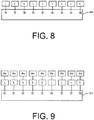
- FIG. 8 illustrates an embodiment of a substrate 800 having silicon atoms at a surface bonded to a linking moiety (illustrated as "L" in FIG. 8 ).
- the linking moiety may be bonded to silicon atoms at the surface of a substrate, such as the substrate 200 of FIG. 2 , the substrate 300 of FIG. 3 , or the substrate 400 of FIG. 4 , by subjecting the substrate to one or more of the processes described with respect to operation 104 in FIG. 1 to treat the surface of the substrate to produce a modified surface of the substrate.
- FIG. 9 illustrates an embodiment of a substrate 900 having silicon atoms at a surface bonded to a linking moiety (illustrated as “L” in FIG. 9 ) and an arsenic-containing compound (illustrated as “As” in FIG. 9 ) is bonded to the linking moiety.
- the arsenic-containing compound may be bonded to the linking moiety by one of the processes described herein with respect to operation 106 of FIG. 1 .
- substrates formed according to embodiments described herein may have certain advantages over the state of the art.
- substrates formed according to embodiments described herein may have a more uniform distribution of dopant atoms than the distribution provided by conventional processes, such as ion implantation.
- concentration of the dopant in the substrate can be controlled by using blocking molecules or by using multiple layers of arsenic-containing compounds bonded to atoms of the surface of the substrate.
- the depth of the diffusion of the dopant atoms can be controlled such that semiconductor devices with ultra-shallow junctions less than 14 nm can be formed.
- the ultra-shallow junctions may be formed due to the decreased damage to the substrate prior to the annealing process, which may limit transient enhanced diffusion that is often present when conventional doping techniques, such as ion implantation or knock-in processes are utilized.
- a composition of matter having the chemical formula: is formed when about 3.047 g (22 mmol) of cacodylic acid and about 2.32 g (22 mmol) of diethanolamine are suspended in about 60 mL of toluene and heated to reflux with azeotropic removal of water using a Dean-Stark apparatus under an atmosphere of nitrogen for about 16 hours. After cooling to about 18-25°C, the toluene is removed in vacuo to produce a substance including the composition of matter. The substance appears as a red oil and 1H NMR analysis shows the substance to have residual impurities, such as toluene and diethanolamine.
- a composition of matter having the chemical formula: is formed when about 2.875 g of cacodylic acid and about 2.77 g of iminodiacetic acid are suspended in 60 mL of toluene in a 100 mL roundbottomed flask fitted with a 10 mL Dean-Stark trap, a nitrogen bubbler and a magnetic stirrer. The mixture is heated at reflux for about 18 hours via oil bath with azeotropic removal of about 0.7 mL - about 0.8 mL of water. After cooling to room temperature, the toluene is removed in vacuo to form a substance that appears as a colorless crystalline solid. 1HNMR (dmso d6) analysis indicates that the composition of matter is formed in near-quantitative yield with 4.916 g being isolated.
- a composition of matter having the chemical formula: is formed when about 1.741 g of allylarsonic acid and about 2.479 g of pinacol are suspended in about 60 mL of toluene and heated at reflux with azeotropic removal of water overnight. Gravity filtration of a small amount of suspension and removal of the toluene in vacuo from the filtrate produce about 3.6 g of a substance that appears as a colorless oil.
- a composition of matter having the chemical formula: is formed when about 6.1 g of (4-hydroxy-3-nitrophenyl)arsonic acid and about 6.13 g of 3-(alloxy)propane-1,2-diol are suspended in about 60 mL of toluene and heated to reflux with the azeotropic removal of water for about 16 hours. After cooling, the toluene is removed in vacuo to give about 11 g of a substance that includes the composition of matter. The substance appears as a yellow oil.
- a composition of matter having the chemical formula: is formed when about 4.36 g of 4-hydroxyphenylarsonic acid and about 4.73 g of pinacol are refluxed together in about 80 mL of toluene for about 16 hours with removal of the water using a Dean-Stark trap. The toluene is removed in vacuo to produce about 7.47 g of a pale yellow crystalline solid.
- a composition of matter having the chemical formula: is formed when about 0.52 g of the bis-pinacol adduct of phenol-4-arsonic acid from Example 5 is treated with about 0.39 g of potassium carbonate and about 1 mL of allyl bromide in about 5 mL of dimethylformamide and swirled briefly. The mixture is allowed to stand at about 18°C to about 25°C for about a week. About 3-5mLs of glacial acetic acid are then added to the mixture with a few drops of 33% HBr in HOAc. Water is added to precipitate the product as colorless needles. The needles are filtered and washed with a little aqueous ethanol. The yield is about 0.40 g after drying in air on the suction filter for about 16 hours.
- a composition of matter having the chemical formula: is formed when about 2.70 g (6.74 mmol) of the bis-pinacol adduct of phenol-4-arsonic acid of Example 5, about 1.66 g (12.01 mmol) of potassium carbonate, and about 0.725 mL (7.66 mmol) of methyl bromoacetate are stirred by magnetic stirrer together in about 10.5 mL of anhydrous dimethylformamide overnight.
- the heterogeneous mixture is diluted with about 20 mL of glacial acetic acid and treated with a few drops of 33% HBr in HOAc. About 80 mL of water is added and the mixture is stirred briefly. The resulting colorless precipitate is removed by vacuum filtration, and washed with a water/ethanol mixture to yield 1.95 g of a substance including the composition of matter after drying.
- a composition of matter having the chemical formula: is formed when about 3.32 g of allyarsonic acid and about 4.16 g of hydroxyisobutyric acid are refluxed under N 2 overnight in about 60 mL of toluene with azeotropic removal of water using a Dean/Stark trap. After removal of solvent, the product is isolated as about 5.55 g of colorless crystals. Another 250 mg is recovered after re-dissolving a remainder from the original flask and evaporation in a smaller vessel.
- a composition of matter having the chemical formula: is formed when about 4.05 g (18.66 mmol) of p-arsinilic acid is slurried in about 40 mL of absolute ethanol and about 4.45 g (22.41 mmol) of solid methyl terephthaloyl chloride is added to the mixture. The mixture is stirred at room temperature, with perhaps a very, very mild exothermic reaction upon addition/dissolution of the acid chloride. Upon complete dissolution in about 5 min, about 1 -3 mL of water is added dropwise and the product precipitates as a colorless powder. The precipitate is removed by suction filtration and dried on the filter for about 16 hours to yield about 3.96 g of the product. Two more crops of about 0.9 g and about 1.1 g of the product are recovered. A 1HNMR analysis indicates that the additional crops have a small amount of contamination of p-arsinilic acid.
- a composition of matter having the chemical formula: is formed when about 3 g of phenylarsonic acid and about 2.79 g of 2-amino-2-methylpropan-1-ol are suspended in about 60 mL of toluene and heated to reflux with the azeotropic removal of water for about 16 hours. After cooling, the toluene is removed in vacuo to produce about 4.83 g of the desired adduct as a colorless, but slightly sticky, crystalline solid. The solid is reslurried in about 60 mL of hexanes at room temperature, and then subject to suction filtration on a coarse frit by washing three times on the filter with about 20 mL of hexanes for each wash. After drying, the desired compound is isolated as about 4.03 g of colorless crystals.
- a composition of matter having the chemical formula: is formed when about 1.707 g of allylarsonic acid and about 1.93 g of 2-amino-2-methyl-1-propanol are suspended in about 60 mL of toluene and heated at reflux under nitrogen with azeotropic removal of water for about 16 hours. After cooling, the toluene is removed in vacuo to produce about 3 g of a semi-solid off-white residue. The residue is boiled briefly in about 60 mL of hexanes, and, after cooling to about 18-25°C, near-colorless needles are formed, collected by suction filtration and washed with hexanes to yield about 1.15 g of the product.
- a composition of matter having the chemical formula: is formed when at room temperature, about 0.5 g (0.445 mL, 2.414 mmol, 1.1 equivalents) of tris(dimethylamino)arsine (TDMA), is added to about 10 mL dry hexane in a 25 mL round-bottom flask, and then about 0.29 g (0.27 mL, 2.19 mmol, 1.0 equivalents) of 3-(allyloxy)propane-1,2-diol is added dropwise into the system. The mixture is heated to reflux under nitrogen for about one hour, and then cooled to room temperature. Removal of the solvent in vacuum gives crude 4-((allyloxy)methyl)-N,N-dimethyl-1,3,2-dioxarsolan-2-amine as an oil.
- TDMA tris(dimethylamino)arsine
- a composition of matter having the chemical formula: is formed when about 0.47 g (4.5 mmol, 1.0 equivalents) of 2,2-dimethylpropane-1,3-diol is added to about 15 mL hexane, and then about 1.04 g (0.92 mL, 5.0 mmol, 1.1 equivalents) of tris(dimethylamino)arsine (TDMA) is added dropwise to the flask. The mixture is heated to reflux under nitrogen for about 1.5 hours, and then cooled to room temperature. Removal of the solvent in vacuum gives crude N,N ,5,5-tetramethyl-1,3,2-dioxarsinan-2-amine as an oil.
- TDMA tris(dimethylamino)arsine
Landscapes
- Chemical & Material Sciences (AREA)
- Organic Chemistry (AREA)
- Cleaning Or Drying Semiconductors (AREA)
- Crystallography & Structural Chemistry (AREA)
- Polymerisation Methods In General (AREA)
- Engineering & Computer Science (AREA)
- Compositions Of Macromolecular Compounds (AREA)
- Materials Engineering (AREA)
- Metallurgy (AREA)
- Chemically Coating (AREA)
- Organic Low-Molecular-Weight Compounds And Preparation Thereof (AREA)
- Semiconductor Memories (AREA)
- Application Of Or Painting With Fluid Materials (AREA)
- Crystals, And After-Treatments Of Crystals (AREA)
Description
- Electronic devices typically include one or more components that are formed from semiconductor wafers. The semiconductor wafers include a number of transistors, sometimes on the order of thousands of transistors up to billions of transistors, to accomplish the functions of the electronic devices. In some cases, electronic device designers often attempt to improve the performance of electronic devices and/or increase the functionality of electronic devices while reducing cost, by adding more transistors to semiconductor wafers.
- Semiconductor device manufacturers have responded by continuing to decrease the size of the transistors formed on the semiconductor wafers. However, the extent of the decrease in size of the transistors may be limited due to limitations of processes used to form certain components of the transistor. For example, the decrease in size of the p-type or n-type junctions of a transistor may be limited due to the ability of semiconductor manufacturers to effectively dope semiconductor wafers such that the concentration of the dopant in the semiconductor wafer is uniform and at a shallow enough depth to support a smaller junction size.
- In particular, as the need for the depth of junctions of transistors to decrease below the 14 nm mark has increased and as transistors have been formed in three-dimensional shapes (e.g. finFETs), semiconductor manufacturers have encountered problems forming properly doped junctions and source/drain extensions, when using traditional doping methods, such as ion implantation. For example, ion implantation of dopants can damage the surface of the substrates, which affects the performance of the junction. Ion implantation may also suffer from limited lateral diffusion control resulting in greater short channel effects which decrease transistor performance. Additionally, since ion implantation is a line of sight doping technique, as the features of three-dimensional transistors decreases, the ion implantation devices are unable to access the entire surface of the substrate, which leads to a non-uniform doping of the substrate surface. When the junctions of transistors included in electronic devices are not uniformly doped, the performance of electronic devices including these transistors can decrease due to the inability of the transistors to signal discrete on and off states. The document
US 2012/0003826 A1 discloses compositions and methods for doping silicon substrates by treating the substrate with a diluted dopant solution comprising tetraethylene glycol dimethyl ether (tetraglyme) and a dopant-containing material and subsequently diffusing the dopant into the surface by rapid thermal annealing. The dopant-containing material may comprise arsenic material. - This summary is provided to introduce simplified concepts of formulations of solutions and processes to form a substrate having a dopant comprising arsenic. Additional details of example formulations of solutions and example processes are further described below in the Detailed Description. This summary is not intended to identify essential features of the claimed subject matter, nor is it intended for use in determining the scope of the claimed subject matter.
- There is provided a process including preparing a solution comprising a dopant and a solvent, wherein the dopant comprises arsenic containing compounds as further described below. The process may also include contacting a substrate with a solution comprising a solvent and a dopant comprising arsenic containing compounds as further described below. The solution may have a flashpoint that is at least approximately equal to a minimum temperature capable of causing attachment between atoms at a surface of the substrate and an arsenic-containing compound in the solution within a duration of at least 2 hours.
- There is also provided a solution comprising a solvent and an arsenic-containing compound as further described below. The solution may have a flashpoint that is at least approximately equal to a minimum temperature capable of causing attachment between atoms of a substrate and an arsenic-containing compound as further described below in the solution.
- There is also provided a substrate may include a surface having a plurality of atoms such as silicon atoms and an arsenic-containing compound as further described below covalently bonded to at least a portion of the plurality of the silicon atoms.
- There is also provided a composition of matter for a variety of arsenic containing compounds as further described below. The dopant in the process, the solution, and the substrate may include any one of these compounds.
- The detailed description is set forth with reference to the accompanying figures. In the figures, the left-most digit(s) of a reference number identifies the figure in which the reference number first appears. The use of the same reference numbers in different figures indicates similar or identical items or features.
-
FIG. 1 is a flow diagram of a process to form a substrate including a dopant. -
FIG. 2 illustrates a substrate having silicon atoms at a surface that can undergo one or more processes described herein. -
FIG. 3 illustrates a substrate having silicon atoms at a surface that have been subjected to one or more processes described herein. -
FIG. 4 illustrates a substrate having silicon atoms at a surface that have been subjected to one or more processes described herein. -
FIG. 5 illustrates a substrate having silicon atoms at a surface bonded to an arsenic-containing compound. -
FIG. 6 illustrates a substrate having silicon atoms at a surface bonded to multiple layers of an arsenic-containing compound. -
FIG. 7 illustrates a substrate having silicon atoms at a surface bonded to a blocking molecule. -
FIG. 8 illustrates a substrate having silicon atoms at a surface bonded to a linking moiety. -
FIG. 9 illustrates a substrate having silicon atoms at a surface bonded to a linking moiety with an arsenic-containing compound bonded to the linking moiety. - This disclosure describes formulations of solutions and processes to form a substrate including a dopant. The dopant includes arsenic (As). Substrates doped with arsenic may have improved electrical characteristics versus the electrical characteristics of phosphorous doped substrates. For example, the diffusion coefficient for As is significantly lower than the diffusion coefficient for other dopants, such as P. Thus, using As as a dopant may produce doped substrates with junctions that are shallower than doped substrates that include other n-type dopants. Additionally, using As as a dopant may produce a doped substrate that is able to withstand higher temperatures before diffusion of the dopant atoms occurs than substrates that include other n-type dopants. Accordingly, arsenic doped substrates can have improved performance with respect to substrates doped with phosphorous. In some cases, arsenic doped substrates can be used to produce semiconductor wafers that may be used in high performance electronic devices. Furthermore, this disclosure describes formulations and processes that may be used to form a uniformly doped substrate that may include three-dimensional transistor structures with junctions having depths less than 20 nm. In some cases, the substrates may include silicon-on-insulator substrates, germanium-on-insulator substrates, conventional silicon substrates, silicon substrates that may present multiple crystal orientations (e.g., substrates having a triangular shaped fin where the orientation of Si atoms may be a function of the position of the Si atoms on the three dimensional structure), conventional germanium substrates, or a combination thereof.
-
FIG. 1 is a flow diagram of aprocess 100 to form a substrate including an arsenic-containing dopant. The substrate may be rigid or the substrate may be flexible. Additionally, the substrate may include a semiconducting material. For example, the substrate may be a silicon containing substrate. The substrate may be a germanium-containing substrate. The substrate may include a combination of silicon and germanium. The substrate may include at least 40% silicon, at least 55% silicon, or at least 70% silicon. If desired, substantially all of the substrate may include silicon, no greater than about 95% of the substrate may include silicon, or no greater than about 80% of the substrate may include silicon. In one non-limiting illustrative example, Si atoms of the substrate may have a 100 orientation. In another non-limiting illustrative example, Si atoms of the substrate may have a 111 orientation. In yet another non-limiting illustrative example, Si atoms of the substrate may have a 110 orientation. - At 102, the
process 100 includes preparing a solution that includes a solvent and a dopant. In some instances, the solution that includes the solvent and the dopant may be referred to herein as a "dopant solution." The dopant includes at least one arsenic atom. The dopant includes an arsenic-containing compound as further described below. The arsenic-containing compound may include an inorganic arsenic-containing compound, an organoarsenic compound, or an organic arsenic-containing compound. - In some cases, the arsenic-containing compound may include at least one functional group that is capable of reacting with atoms at the surface of a substrate and/or is capable of interacting with atoms at the surface of the substrate. The at least one functional group of the arsenic-containing compound may react and/or interact with atoms at the surface of the substrate via chemisorption, physisorption, or both. The reaction and/or interaction between the at least one functional group of the arsenic-containing compound and atoms at the surface of the substrate may include covalent bonding, dative bonding, hydrogen bonding, ionic bonding, or a combination thereof. In some situations, the arsenic-containing compounds and the atoms at the surface of the substrate may have a localized or supramolecular interaction that is sufficiently strong such that the arsenic-containing compound remains at the surface of the substrate when subjected to some subsequent processing conditions. In other instances, the reaction and/or interaction between the arsenic-containing compound and the atoms at the surface of the substrate may be disrupted when subjected to other subsequent processing conditions, such as the conditions of an annealing process. In this way, the arsenic atoms may be released and available to diffuse into the substrate.
- The reactive functional group or groups may include an alkenyl group, an alkynyl group, a hydroxyl group, an aryl group, an amine group, an amide group, a nitro group, a carbonyl group, a halogen-containing group, a thiol group, a dienophile, or a combination thereof. If desired, the arsenic-containing compounds may include one or more As(III) atoms. Alternatively, the arsenic-containing compounds may include one or more As(V) atoms. If desired, the arsenic-containing compounds may include one or more As(III) atoms and one or more As(V) atoms. In some cases, the arsenic-containing compound may be a polyarsenic compound.
- The arsenic-containing compounds described herein may be formed using a number of techniques. In some cases, the arsenic-containing compounds may be formed from a condensation reaction. Illustrative examples of preparative methods that may be used to form arsenic-containing compounds are described in Doak, G.O. ; Freedman, L.D. Organometallic compounds of arsenic, antimony, and bismuth in; Seyferth, Dietmar, Ed. The Chemistry of Organometallic Compounds; Wiley-Interscience: New York, 1970; Chemistry of Arsenic, Antimony and Bismuth; Norman, N.C., Ed. Blackie Academic & Professional: London, 1998; and Raiziss, G.W. ; Gavron, J.L. Organic Arsenical Compounds; American Chemical Society Monograph Series; Chemical Catalog Company: New York, 1923, which are herein incorporated by reference in their entirety. Other illustrative examples of preparative methods of arsenic-containing compounds described herein are described in Loiseau, P.M., Rekik, L, Madaule, Y., Gayral, P., and Wolf, J.G. Arzneim.-Forsch./Drug Res. 43(11), Nr. 9 (1993) 1004-1009; Dale, Arild J., and Froyen, Paul Acta Chemica Scandanavica B 29 (1975) 741-748; Tapia-Benavides, Antonio R. ; Mendoza-Huizar, Luis H. ; Perez-Garcia, Francisco; Tlahuext, Hugo; Alvarez, Alejandro; and Tlahuextl, Margarita. Inorg. Chem. 2010, 49, 1496-1502; and Betz, Richard and Klufers, Peter. Inorg. Chem. 2009, 48, 925-935. If desired, the arsenic-containing compound may include or be formed from arsonic acids, arsinic acids, derivatives of arsonic acids, derivatives of arsinic acids, or combinations thereof. Derivatives of the arsonic acids and/or derivatives of the arsinic acids may include esters, thioesters, amides, ester/amides, thioester/amides, or a combination thereof. If desired, the arsenic-containing compound may include or be formed from arsonous acids; arsinous acids; derivatives of arsonous and/or arsinous acids, such as esters, amides, and/or ester/amides; or combinations thereof. For example, the invention includes arsenic-containing compounds such as those formed from arsines, including aminoarsines, alkylaminoarsines, dialkylaminoarsines, haloarsines, dialkylhaloarsines, and dihaloalkylarsines. The invention also includes arsenic-containing compounds such as arsine oxides, arseno compounds, diarsines, polyarisnes, or combinations thereof. The arsenic-containing compounds may serve as an intermediate to produce a dopant or pre-dopant by further reaction to introduce a moiety or moieties capable of reaction or interaction with the surface or modified surface of the substrate via chemisorption or physisorption.
- Arsinic acids may be derivatized to form certain adducts as shown below:

- Non-limiting examples of compound II above may include glycerol, diethanolamine, iminodiacetic acid, 2-ethyl-2-amino-1,3-propanediol, serinol, 2-methyl-2-amino-1,3-propandiol, and trimethylolpropane.
- Some non-limiting examples of R1 and R2 may include a methyl group, an ethyl group, a higher branched, straight-chain group, a cycloalkyl group, an alkenyl group, an alkynyl group, an allyl group, a propargyl group, a phenyl group, another aryl group, a hetararyl group, or a combination thereof. For example, R1 and R2 may include 4-hydroxyphenyl, 4-allyloxyphenyl, 4-propargyloxyphenyl, 3-acetamido-4-hydroxyphenyl, 3-amino-4-hydroxyphenyl, 4-aminophenyl, 3-acetamido-4-allyloxyphenyl, 3-acetamido-4-propargyloxyphenyl, 3-nitro-4-hydroxyphenyl, 3-nitro-4-allyloxyphenyl, 3-nitro-4-propargyloxyphenyl, 4-aminophenyl, 4-allylaminophenyl, 4-diallylaminophenyl, 4-propargylaminophenyl, 4-dipropargylaminophenyl, 4-allyloxy-3-allylaminophenyl, 4-allyloxy-3-diallylaminophenyl, 4-propargyloxy-3-dipropargylaminophenyl, 4-maleimidophenyl, 4-hydroxy-3-maleimidophenyl, 4-acrylamidophenyl, 4-methacrylamidophenyl, 4-(2-methoxy-2-oxoethoxy)phenyl, or 4-(4-(methoxycarbonyl)benzamidophenyl)phenyl.
- Arsonic acids, such as compound IV below, may be derivatized to form certain adducts, such as compound VII below, by reaction with compounds V and VI as shown below. If desired, V and VI are the same compound, or V and VI are different compounds.

- Some non-limiting examples of R3 may include a methyl group, an ethyl group, a higher branched, straight-chain group, a cycloalkyl group, an alkenyl group, an alkynyl group, an allyl group, a propargyl group, a phenyl group, another aryl group, a heteroaryl group, or a combination thereof. R3 may include 4-hydroxyphenyl, 4-allyloxyphenyl, 4-propargyloxyphenyl, 3-acetamido-4-hydroxyphenyl, 3-amino-4-hydroxyphenyl, 4-aminophenyl, 3-acetamido-4-allyloxyphenyl, 3-acetamido-4-propargyloxyphenyl, 3-nitro-4-hydroxyphenyl, 3-nitro-4-allyloxyphenyl, 3-nitro-4-propargyloxyphenyl, 4-aminophenyl, 4-allylaminophenyl, 4-diallylaminophenyl, 4-propargylaminophenyl, 4-dipropargylaminophenyl, 4-allyloxy-3-allylaminophenyl, 4-allyloxy-3-diallylaminophenyl, 4-propargyloxy-3-dipropargylaminophenyl, 4-maleimidophenyl, 4-hydroxy-3-maleimidophenyl, 4-acrylamidophenyl, 4-methacrylamidophenyl, 4-(2-methoxy-2-oxoethoxy)phenyl, 4-(4-(methoxycarbonyl)benzamidophenyl)phenyl.
- Some non-limiting examples of compounds V and VII above are ethylene glycol, propylene glycol, pinacol, mercaptothanol, ethylenediamine, ethanedithol, catechol, 1 ,2-diaminobenzene, ortho-aminothiophenol, ethanolamine, 2-amino-2-methyl-1-propanol, 2-hydroxyisobutyric acid, 2-aminoisobutyric acid, 2-aminophenol, N-methylethanolamine, 3-allyloxy-1,2-propanediol, 3-amino-4-hydroxyphenylarsonic acid, arsphenamine, 3-amino-4-hydroxyphenylarsonic acid, 2-(tert-butylamino)ethanol, or combinations thereof.
- If desired, certain arsines, in particular, di- or trihaloarsines and/or bis- or trisaminoarsines may be further derivatized with bis nucleophiles. For example, bis nucleophiles, such as compound VIII (HE9-G4-E8H), can react with trisdialkylaminoarsines to give a composition of matter of Formula IX:

- Some non-limiting examples of compound VIII may include ethylene glycol, propylene glycol, pinacol, mercaptothanol, ethylenediamine, ethanedithol, catechol, 1 ,2-diaminobenzene, ortho-aminothiophenol, ethanolamine, 2-amino-2-methyl-1-propanol, 2-hydroxyisobutyric acid, 2-aminoisobutyric acid, 2-aminophenol, N-methylethanolamine, 3-allyloxy-1,2-propanediol, 3-amino-4-hydroxyphenylarsonic acid, arsphenamine, 3-amino-4-hydroxyphenylarsonic acid, 2-(tert-butylamino)ethanol, N,N-bis(hydroxyethyl)-4-propargylyloxyaniline, and N,N-bis(hydroxyethyl)-4-allyloxyaniline.
- Table 1 includes illustrative examples of arsenic-containing compounds of which the compounds with the numbers 8 to 19 and 29 are inventive and may be utilized in the processes, solutions, and the substrates of the inventions described herein. In addition, the arsenic-containing compounds that may be utilized in the inventions may, if desired, include ions of the compounds listed in Table 1, salts of the compounds listed in Table 1, or a combination thereof.
Table 1 Compound Number Molecular Weight Structure 1 207.15 
2 
3 
4 138 
5 202.04 
6 166.01 
7 384.34 
8 326.27 
9 290.23 
10 348.31 
11 235.07 
12 473.31 
13 400.34 
14 320.17 
15 472.4 
16 379.2 
17 440.41 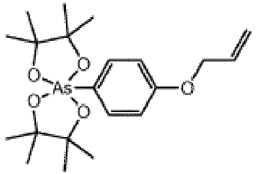
18 
19 
20 
21 
22 
23 
24 
25 
26 
27 
28 
29 
- In Table 1 , each R, may independently, include hydrogen, a hydrocarbyl group, a substituted hydrocarbyl group, or a silyl group. In addition, two or more R groups taken together may collectively form a bridging group. Further, in Table 1, each R' group, may independently, include hydrogen, a hydrocarbyl group, a substituted hydrocarbyl group, or a silyl group. Additionally, two or more R' groups taken together may collectively form a bridging group. E in Table 1 may, independently include N, O, or S atoms. In situations when E is N, then N may be further substituted by hydrogen, a hydrocarbyl group, a substituted hydrocarbyl group, or a silyl group. In Table 1, G may represent a group linking two or more atoms represented by E; and G may include a hydrocarbyl group, a substituted hydrocarbyl group, or a silyl group. Furthermore, in Table 1, X may include a halogen atom.
- If desired, a solvent included in the dopant solution is capable of dissolving the dopant or the dopant may be miscible in the dopant solution at a temperature of no greater than about 50°C, no greater than about 42°C, no greater than about 35°C, no greater than about 30°C, or no greater than about 25°C. Desirably, the solvent is capable of dissolving the dopant at a temperature of at least 2°C, at least 8°C, at least 15°C, or at least about 20°C. For example, the solvent may be capable of dissolving the dopant at a temperature within a range of about 20°C to about 35°C.
- Examples of solvents include 4-hydroxy butanoic acid, a glycol ether (e.g., di-ethylene glycol di-butyl ether, tetra-ethylene glycol di-methyl ether (tetraglyme)), 4-formylmorpholine, phenylacetic acid, a C9 alcohol, a C10 alcohol, 3-nonanone, phenylpropyl ether, dimethylsulfoxide (DMSO), cyclooctanone, furfuryl acetone, isophorone, di-hexyl ether, 2-nonanone, phenyl propyl ether, hexyl benzene, mesitylene, N-methylpyrrolidone (NMP), an alkanolamine, acetonitrile, toluene, dioxane, tetrahydrofuran (THF), or combinations thereof. In some cases, the solvent may include an inert compound, such as methanol, ethanol, isopropanol, ethylene glycol, propylene glycol, glycerine, ethyl acetate, propyl acetate, methyl acetate, acetone, methyl ethyl ketone, methyl butyl ketone, or combinations thereof.
- In particular instances, the solvent may include an amount of water. In some cases, the amount of water included in the solvent may be minimized. For example, the preparation of the solution at 102 may include drying the solvent. To illustrate, the solvent may be dried by adding a drying agent to the solvent. The drying agent can include an inorganic salt, a zeolite, a water reactive compound, or a combination thereof. In another illustration, the solvent may be dried by washing the solvent with a drying solution. In additional illustrative examples, the solvent may be dried via distillation in the presence of a drying agent in an ambient environment or while pulling a vacuum, via distillation of water from the solvent in an ambient environment or while pulling a vacuum, via rotary evaporation techniques, via thin-film evaporation techniques, via azeotropic distillation techniques, or a combination thereof. The solvent that is selected may be non-hygroscopic if desired.
- The solvent may include no greater than about 10 vol% water for a total volume of the solvent, no greater than about 7 vol% water for a total volume of the solvent, no greater than about 4 vol% water for a total volume of the solvent, or no greater than about 1 vol% water for a total volume of the solvent. The solvent can include water within a range of 0.05 vol% water to about 2.5 vol% water for a total volume of the solvent. The solvent may be sufficiently dry such that a precipitate is not formed when the dopant and solvent are mixed at suitable process conditions.
- If desired, the dopant solution can be formulated to have a flashpoint that is at least approximately equal to or greater than a minimum temperature capable of causing attachment between at least a portion of the atoms at a surface of a substrate and an arsenic-containing compound in the dopant solution. The attachment may occur in conjunction with a reaction between the arsenic-containing compound in the dopant solution and the atoms at the surface of the substrate. If desired, the arsenic-containing compound may attach to at least 5% of the atoms at the surface of the substrate, at least 20% of the atoms at the surface of the substrate, at least 50% of the atoms at the surface of the substrate, at least 80% of the atoms at the surface of the substrate, or at least 95% of the atoms at the surface of the substrate, or to essentially all of the atoms at the surface of the substrate.
- The flashpoint of the dopant solution may be at least 40°C, at least 55°C, at least 75°C, at least 100°C, at least 125°C, at least 150°C, or at least 200°C. For example, the flashpoint of the dopant solution is within a range of about 50°C to about 115°C, or within a range of about 110°C to about 250°C.
- The flashpoint of the dopant solution may be at least 10°C, at least 35°C, at least 50°C, or at least 75°C greater than the minimum temperature capable of causing attachment between atoms at a surface of the substrate and the arsenic-containing compound of the dopant solution. The flashpoint of the dopant solution can be no greater than 200°C, no greater than 175°C, no greater than 140°C, or no greater than 100°C greater than the minimum temperature capable of causing attachment between atoms at a surface of the substrate and the arsenic-containing compound of the dopant solution. The flashpoint of the dopant solution may be within a range of about 25°C to about 150°C or within a range of about 40°C to about 80°C greater than the minimum temperature capable of causing attachment between atoms at a surface of the substrate and the arsenic-containing compound of the dopant solution.
- In some situations, the flashpoint of the solution may be at least a temperature that is capable of causing attachment between atoms at the surface of the substrate and the arsenic-containing compound of the dopant solution within a duration of at least 2 hours, at least 2.5 hours, at least 3 hours, at least 5 hours, or at least 7.5 hours. Further, the flashpoint of the solution may be at least a temperature that is capable of causing attachment between atoms at the surface of the substrate and the arsenic-containing compound of the dopant solution within a duration of no greater than 15 hours, no greater than 12 hours, no greater than 10 hours, or no greater than 8 hours. The flashpoint of the solution may be at least a temperature that is capable of causing attachment between atoms at the surface of the substrate and the arsenic-containing compound of the dopant solution within a duration having a range of about 1.5 hours to about 10 hours. The flashpoint of the solution may be at least a temperature that is capable of causing attachment between atoms at the surface of the substrate and the arsenic-containing compound of the dopant solution within a duration having a range of about 2.5 hours to about 5 hours. In some scenarios, the flashpoint of the solution may be at least a temperature that is capable of causing attachment between atoms at the surface of the substrate and the arsenic-containing compound of the dopant solution at a pressure within a range of 344.7 hPa (5 pounds per square inch (psi)) to 3447 hPa (50 psi).
- If desired, the solution can include at least 1 wt% dopant of a total weight of the dopant solution, at least 5 wt% dopant of a total weight of the dopant solution, at least 15 wt% dopant of a total weight of the dopant solution, or at least 30 wt% dopant of a total weight of the dopant solution. If desired, the solution includes no greater than about 60 wt% dopant of a total weight of the dopant solution, no greater than about 50 wt% dopant of a total weight of the dopant solution, no greater than about 42 wt% dopant of a total weight of the dopant solution, or no greater than about 35 wt% dopant of a total weight of the dopant solution. The solution can include dopant within a range of about 2 wt% to about 11 wt% of a total weight of the dopant solution, or within a range of about 25 wt% to about 40 wt% of a total volume of the dopant solution. If desired, substantially all of the dopant solution can include the dopant.
- The dopant solution can be prepared by mixing the solvent and the dopant at a suitable temperature and pressure such that the solvent dissolves the dopant or the dopant is miscible in the solvent. For example, the solvent and the dopant can be mixed at a temperature of at least 10°C, at least 18°C, at least 25°C, or at least 30°C. In another example, the solvent and the dopant may be mixed at a temperature of no greater than about 50°C, no greater than about 42°C, or no greater than about 35°C. In an illustrative embodiment, the dopant and the solvent can be mixed at a temperature within a range of about 17°C to about 30°C. Further, the dopant and the solvent can be mixed at a pressure within a range of 689.5 hPa (10 pounds/in.2 (psi)) to 1723 hPa (25 psi).
- At 104, the
process 100 includes treating a surface of the substrate to produce a modified surface of the substrate. Treating the surface of the substrate may include contacting the surface with a material that is capable of modifying the bonds of atoms at the surface of the substrate. "Contacting" as used herein may refer to one or more processes for bringing the surface of the substrate into physical contact with a material, such as immersion, spin coating, spraying, vapor exposure, and the like. - Atoms at the surface of the substrate may oxidize when exposed to air forming an oxide at the surface of the substrate. In some cases, treating the surface of the substrate may include removing at least a portion of the oxide with a particular material. The surface of the substrate can be treated with an acidic solution to replace at least a portion of the oxidized portions of the surface with hydrogen-terminated atoms. A first portion of the atoms on the surface of substrate may undergo hydrogen termination, while a second portion of the atoms of the surface of the substrate may remain oxidized. In certain situations, the acidic solution can include a hydrofluoric acid, such as a dilute hydrofluoric acid. The substrate may be treated with the acidic solution for a duration of at least 1 minute, at least 3 minutes, or at least 5 minutes. The substrate may be treated with the acidic solution for no greater than 15 minutes, no greater than 12 minutes, or no greater than 8 minutes. In a non-limiting illustrative embodiment, the substrate may be treated with the acidic solution for a duration within a range of about 2 minutes to about 6 minutes. The substrate may be treated with the acidic solution at a temperature within a range of about 10°C to about 35°C, optionally in an inert environment, such as a N2 environment, and/or the substrate may be treated with an acidic solution that has been de-aerated.
- The surface of the substrate may be treated with other materials to modify the surface of the substrate. In some situations, the substrate may undergo multiple treatments with certain materials to modify the surface of the substrate. Additionally, the surface of the substrate may be modified such that endgroups on the surface of the substrate are reactive toward the arsenic-containing compounds included in the dopant solution prepared with respect to
operation 102. In one illustrative example, the surface of the substrate may include a number of silicon atoms that are treated in such a way that silanols are formed followed by contacting the substrate with a solution that includes an ester-containing molecule. In another illustrative example, the surface of the substrate may be contacted with a nitric acid and hydrogen peroxide solution. If desired, the amount of nitric acid in the nitric acid and hydrogen peroxide solution can be within a range of about 10 vol% to about 40 vol% of a total volume of the nitric acid and hydrogen peroxide solution. The surface of the substrate may be contacted with an aqueous nitric acid solution. An amount of nitric acid in the aqueous nitric acid solution may be within a range of about 10 vol% to about 70 vol% of a total volume of the aqueous nitric acid solution. In further illustrative examples, atoms at the surface of the substrate may be treated to form hydrides followed by contacting the substrate with a solution that can include an allyl-containing molecule. To illustrate, silicon atoms at the surface of the substrate may be treated to form silicon hydrides and then undergo hydrosilylation by contacting the surface of the substrate with an allyl-containing solution to form a silicon-alkyl bond. Other illustrative examples of the chemical modification of the surface of a substrate that may be used are described in, Timothy R. Leftwich, Andrew V. Teplyakov. "Chemical Manipulation of Multifunctional Hydrocarbons on Silicon Surfaces." Surface Science Reports 63 (2008): 1-71. - The surface of the substrate may be modified by contacting the surface with a solution for a duration of at least 2 minutes, at least 5 minutes, at least 20 minutes, or at least 45 minutes. The surface of the substrate may be modified by contacting the surface with a solution for a duration of no greater than about 125 minutes, no greater than about 100 minutes, or no greater than about 75 minutes. The surface of the substrate may be modified by contacting the surface with a solution for a duration within a range of about 40 minutes to about 80 minutes.
- Further, the surface of the substrate may be modified by contacting the surface with a solution at a temperature of at least 25°C, at least 55°C, or at least 80°C. In other situations, the substrate may be modified by contacting the surface with a solution at a temperature of no greater than about 150°C, no greater than about 120°C, or no greater than about 95°C. The surface of the substrate may be modified by contacting the surface at a temperature within a range of about 65°C to about 100°C.
- In some instances, treating the surface of the substrate to produce a modified surface of the substrate may include one or more rinse cycles, one or more drying cycles, or a combination thereof. In one example, after hydrosilylation of the surface of the substrate, the substrate may be rinsed with a solution including a solvent. The solvent can include isopropyl alcohol, mesitylene, and/or DMSO. In another example, after modification of the surface of the substrate, the substrate may be rinsed with de-ionized water. Additionally, the substrate may be rinsed after contacting the surface of the substrate with a surface modification solution. After a rinsing cycle, the substrate may be dried. The substrate may be dried via air drying, Marangoni drying, spin drying, contacting the substrate with a stream of dry inert gas, or a combination thereof.
- At 106, the
process 100 may include contacting the modified surface of the substrate with the dopant solution prepared with respect tooperation 102. Contacting the modified surface of the substrate with the dopant solution may cause a reaction between atoms of the modified surface of the substrate and the arsenic-containing molecules in the dopant solution. In this way, arsenic-containing compounds can be chemisorbed or physisorbed to atoms at the surface of the substrate. In particular, the arsenic-containing compounds may have a localized or supramolecular interaction that is sufficiently strong such that the arsenic-containing compound remains on the surface of the substrate when subjected to subsequent processing. In some cases, the interaction between the arsenic-containing compound and the atoms at the surface of the substrate may include covalent bonding, dative bonding, hydrogen bonding, ionic bonding, or a combination thereof. Particular examples of interactions between arsenic-containing compounds and atoms on the surface of the substrate may include hydrosilylation of alkenes and/or alkynes with surface silanes; ester interchange between ester moieties and surface silanols of other attached hydroxyls; carboxamide formation from an ester and amino functionalized surface; arsonous and/or asinous ester formation from surface silanols and amino arsines, such as trisdimethylaminoarsine; arsonous or arsinous ester formation from surface silanols and arsenic(III)-containing compounds, such as for example, arsenic-amine compounds with no more than 1 arsenic-nitrogen bond, no more than 2 arsenic-nitrogen bonds, or no more than 3 arsenic-nitrogen bonds; or combinations thereof. - The surface of the substrate can be contacted with the dopant solution for a duration of at least 0.05 hours, 0.3 hours, at least 0.9 hours, at least 1.4 hours, or at least 1.8 hours. The surface of the substrate can be contacted with the dopant solution for a duration of no greater than about 3.6 hours, no greater than about 3.1 hours, no greater than about 2.5 hours, or no greater than about 2.2 hours. The surface of the substrate can be contacted with the dopant solution for a duration within a range of about 0.4 hours to about 3.0 hours. In another illustrative embodiment, the surface of the substrate can be contacted with the dopant solution for a duration within a range of about 0.7 hours to about 2 hours.
- The surface of the substrate may be contacted with the dopant solution at a temperature of at least 30°C, at least 55°C, at least 80°C, or at least 105°C. In other embodiments, the surface of the substrate may be contacted with the dopant solution at a temperature of no greater than about 175°C, no greater than about 155°C, no greater than about 135°C, or no greater than about 120°C. The surface of the substrate can be contacted with the dopant solution at a temperature within a range of about 85°C to about 140°C or within a range of about 100°C to about 125°C.
- If desired, the substrate may be rinsed after being contacted by the dopant solution. The substrate may be rinsed with a fresh feed of same type of solvent used in the dopant solution, or even rinsed by re-using the solvent employed in the dopant solution. For example, the substrate may be rinsed with tetraglyme when tetraglyme is used to prepare the solution of 102. In another illustrative example, the substrate can be rinsed with acetonitrile when acetonitrile is used to prepare the solution of 102. In an additional illustrative example, the substrate can be rinsed with THF when THF is used to prepare the solution of 102. In an additional illustrative example, the substrate can be rinsed with n-methylpyrolidone (NMP) when NMP is used to prepare the solution of 102. In certain instances, the substrate may undergo an additional rinse after being rinsed with the solvent included in the dopant solution. If desired, the substrate may undergo an additional rinse using a low boiling point solvent. An example of a low boiling solvent may be isopropanol. In yet another illustrative example, the substrate can be rinsed with water. In certain cases, the substrate may also undergo one or more drying operations. In one case, the substrate may be dried after being contacted with the dopant solution. In another case, the substrate may be dried after being rinsed with the solvent of the dopant solution. In a further scenario, rinsing the substrate with the low-boiling point solvent may be part of a process to dry the substrate. In some cases, the substrate may not undergo rinsing after modifying the surface of the substrate and before contacting the substrate with a dopant solution.
- Rinsing can include contacting the substrate with a heated solvent, such as the solvent included in the dopant solution. The temperature of the solvent may be room temperatures, such as within a range of about 15°C to about 25°C, up to a minimum temperature capable of initiating a reaction between the dopant solution and the substrate within a specified duration. In some cases, the heated solvent may be applied to a substrate after contacting the surface of the substrate with a surface modification solution or after the substrate has been contacted with a dopant solution. After contacting the substrate with the heated solvent, the substrate may be rinsed with either water or a low boiling organic solvent.
- Rinsing the substrate can include contacting the substrate with a solvent and providing sonic energy into the liquid. In some instances, the sonic energy may be ultrasonic or megasonic. The sonic energy may be provided to the solvent for a duration of at least 10 seconds, at least 30 seconds, at least 2 minutes or at least 5 minutes. The sonic energy may be provided continuously or in a pulsed manner, and the frequency may be fixed, swept, or any combination thereof. If desired, the solvent provided with the sonic energy may be the solvent present in the dopant solution, another organic solvent, such as a low boiling organic solvent, or de-ionized water.
- The processes described with respect to
operation 106 can be repeated. To illustrate, after the substrate is contacted with the dopant solution, the substrate may undergo an additional process to contact the substrate with the dopant solution. In some situations, the substrate may be rinsed each time the substrate is contacted with a dopant solution, while in other cases, the substrate may not be rinsed after at least one of the applications of the dopant solution to the substrate. Accordingly, multiple layers of the arsenic-containing compound in the dopant solution may be added to the surface of the substrate. In some instances, the duration and temperature of subsequent operations of contacting the substrate with the dopant solution may be similar to the duration and temperature of a previous operation of contacting the substrate and the dopant solution. In other instances, the duration and temperature of subsequent operations directed to contacting the substrate with the dopant solution may be different than the duration and temperature of a previous operation of contacting the substrate with the dopant solution. Accordingly, the use of more than one dopant solution for the corresponding dopant layers may be employed. - At 108, the
process 100 includes adding the dopant to a body of the substrate. In some cases, the dopant may be added to the body of the substrate via diffusion. In particular instances, arsenic atoms included in the arsenic-containing compounds bonded to the surface of the substrate may diffuse from the surface of the substrate into the body of the substrate under suitable conditions. In some cases, the arsenic-containing compounds bonded to the surface of the substrate may be organoarsenic compounds. In other situations, the arsenic-containing compounds bonded to the surface of the substrate may be inorganic. In a particular instance, organic functional groups of an organoarsenic compound that is bonded to atoms at the surface of the substrate may react with trace amounts of water to cleave the organic functional groups and produce an inorganic arsenic-containing compound. For example, when tris(dimethylamino)arsine (TDMA) is bonded to silanol groups at the surface of the substrate, trace amounts of water may react with the dimethylamine groups of TDMA to remove these organic functional groups. Arsenic atoms diffusing into the body of the substrate may displace silicon atoms, germanium atoms, or both, within the lattice structure of the body of the substrate. - The arsenic atoms may diffuse to a particular depth with respect to the surface of the substrate. In one example, the arsenic atoms may diffuse into the body of the substrate such that the peak concentration of the dopant is achieved at a depth of no greater than about 20 nm from the surface of the substrate, no greater than about 10 nm from the surface of the substrate, no greater than about 7 nm from the surface of the substrate, or no greater than about 4 nm from the surface of the substrate. Additionally, the distribution of dopant in the substrate may be such that substantially no dopant in the silicon is present at a distance of 20 nm from a location of the peak dopant concentration in the substrate, at a distance of 10 nm from a location of a peak dopant concentration in the substrate, at a distance of 7 nm from a location of the peak dopant concentration in the substrate, or at a distance of 5 nm from the a location of the peak dopant concentration in the substrate. The arsenic atoms may diffuse into the body of the substrate such that a location of the peak concentration of arsenic is achieved at a depth within a range of about 0.5 nm to about 9 nm and substantially no arsenic is present at a depth of about 3 nm to about 10 nm from a location of the peak arsenic concentration. The arsenic atoms may diffuse into the body of the substrate to a depth within a range of about 1 nm to about 5 nm.
- Adding the dopant to the body of the substrate may include an anneal process. In some cases, the anneal process may be conducted in an inert gas, such as nitrogen or argon, environment. The anneal process may have a duration of at least 10 milliseconds, at least 0.5 seconds, at least 4 seconds, at least 20 seconds, at least 30 seconds, or at least 45 seconds. The anneal process may have a duration of no greater than 135 seconds, no greater than 100 seconds, no greater than 75 seconds, or no greater than 50 seconds. The anneal process can have a duration within a range of about 10 seconds to about 90 seconds, within a range of about 25 seconds to about 75 seconds, or within a range of about 30 seconds to about 60 seconds, or within a range of about 10 milliseconds to about 700 milliseconds.
- The anneal process can be conducted at a temperature of at least 600°C, at least 750°C, at least 900°C, or at least 1000°C. The anneal process may be conducted at a temperature of no greater than about 1200°C, no greater than about 1 125°C, or no greater than about 1050°C. The anneal process may be conducted at a temperature within a range of about 800°C to about 1150°C or within a range of about 900°C to about 1050°C.
- Prior to the annealing operation, an optional capping layer can be applied to the surface of the substrate. The capping layer may overlie the arsenic-containing compounds bonded to atoms of the substrate. The capping layer may include SiO2. The capping layer can include silicon oxide formed using a plasma enhanced tetraethyl-orthosilicate process. The capping layer can include silicon oxide formed with a liquid spin-on dielectric material. The capping layer may have a thickness of at least 10 nm, at least 25 nm, or at least 40 nm. In other situations, the capping layer may have a thickness no greater than about 100 nm, no greater than about 80 nm, or no greater than about 60 nm. The capping layer may have a thickness within a range of about 15 nm to about 55 nm or within a range of about 25 nm to about 45 nm. After annealing of the substrate, the capping layer may be removed. For example, the capping layer may be removed by contacting the capping layer with a solution of dilute hydrofluoric acid.
- Although the
process 100 includes operations described with respect to blocks 102-108, in some cases, theprocess 100 can include additional operations. To illustrate, once the dopant has been added to the substrate, one or more additional operations can be performed to form a semiconductor device that includes ultra-shallow junctions formed from the doped substrate. In another illustration, the substrate may be contacted with a material that blocks some silicon atoms at the surface of the substrate from forming a bond with the arsenic-containing compound. In a particular situation, the blocking compounds may include reactive moieties that are analogous to those found on the arsenic-containing compound, but the blocking compounds do not include a dopant atom or atoms themselves. - In other cases, the
process 100 may include fewer operations. For example, the operations described with respect to 104 may be removed from theprocess 100 and the substrate can be contacted with the dopant solution without first modifying the surface of the substrate. Additionally, it should be noted that portions of the surfaces of the substrates described with respect to theprocess 100 may include exposed atoms of the substrate, such as exposed silicon atoms and/or exposed germanium atoms, while other portions of the surfaces of the substrate may be covered with particular materials, such as photoresist. Further, the order in which the operations of theprocess 100 are described is not intended to be construed as a limitation, and any number of the described operations can be combined in any order and/or in parallel to implement theprocess 100. The dopant solution may or may not include a solvent. -
FIG. 2 illustrates asubstrate 200 having silicon atoms at a surface that can undergo one or more embodiments of processes described herein. The silicon atoms at the surface of thesubstrate 200 may not yet have been subjected to any processes to modify the surface of thesubstrate 200 as described herein. Thesubstrate 200 illustrates the terminal bonding of silicon atoms at the surface of thesubstrate 200 when exposed to an air environment. Although not illustrated inFIG. 2 , the silicon atoms at the surface of thesubstrate 200 may be bonded to each other, to other atoms of the substrate, or a combination thereof. -
FIG. 3 illustrates asubstrate 300 having silicon atoms at a surface that have been subjected to one or more embodiments of processes described herein. Thesubstrate 300 may illustrate the terminal bonding of silicon atoms at the surface of the substrate after being subjected to a surface modification process, such as a hydrogen termination process or a silanol formation process, as described herein. -
FIG. 4 illustrates an additional embodiment of asubstrate 400 having silicon atoms at a surface that have been subjected to one or more embodiments of processes described herein. In the illustrative embodiment ofFIG. 4 , a portion of the silicon atoms at the surface of thesubstrate 400 are bonded to hydrogen atoms, while a number of other atoms at the surface of thesubstrate 400 are not hydrogenated. The partial hydrogenation of the atoms at the surface of thesubstrate 400 may be due to the exposure of thehydrogenated substrate 300 ofFIG. 3 to an air environment. In another embodiment, the partial hydrogenation of the atoms at the surface of thesubstrate 400 may be due to the incomplete reaction of atoms at the surface of thesubstrate 400 during a hydrogen termination process. In another embodiment, the partial hydrogenation may be a result of exposing a hydrogen terminated surface to an oxidizing liquid. In yet another embodiment, the partial hydrogenation may be a result of the presence of dissolved oxygen in the hydrogen termination solution. In a further embodiment, the partial hydrogenation may be a result of exposing the hydrogen terminated surface to deionized water that contains dissolved oxygen. Combinations of any or all of the above steps are also possible to form partial hydrogenation. -
FIG. 5 illustrates an embodiment of asubstrate 500 having silicon atoms at a surface bonded to an arsenic-containing compound (illustrated as "As" inFIG. 5 ). The silicon atoms at the surface of the substrate may be bonded directly to an As atom of the arsenic-containing compound. In another embodiment, the silicon atoms at the surface of the substrate may be bonded to atoms of the arsenic-containing compound other than the As atom or atoms of the arsenic-containing compound. In a particular embodiment, thesubstrate 500 may have been contacted with one or more of the dopant solutions described herein, such as via the processes described with respect tooperation 106 ofFIG. 1 . -
FIG. 6 illustrates an embodiment of asubstrate 600 having silicon atoms at a surface bonded to multiple layers of an arsenic-containing compound (illustrated as "As" inFIG. 6 ). In a particular embodiment, thesubstrate 600 may represent thesubstrate 500 ofFIG. 5 after being subjected to an additional process of contacting thesubstrate 500 with one or more of the dopant solutions described herein. -
FIG. 7 illustrates an embodiment of asubstrate 700 having silicon atoms at a surface bonded to a blocking molecule (illustrated as "B" inFIG. 7 ). In some cases, to control the concentration of the dopant in thesubstrate 700, a substrate, such as thesubstrate 200 ofFIG. 2 , thesubstrate 300 ofFIG. 3 , or thesubstrate 400 ofFIG. 4 , can be subjected to one or more processes to bond blocking molecules with a portion of the silicon atoms at the surface of the substrate. The blocking molecules may not form a bond with one or more of the arsenic-containing compounds described herein under the process conditions described herein. In a particular embodiment, the blocking compounds may include reactive moieties that are analogous to those found on the arsenic-containing compound, but do not include a dopant atom or atoms themselves. Some examples of blocking molecules include alpha olefins, terminal alkynes, carboxylic esters, acyl halides, isocyanates, or combinations thereof. -
FIG. 8 illustrates an embodiment of asubstrate 800 having silicon atoms at a surface bonded to a linking moiety (illustrated as "L" inFIG. 8 ). The linking moiety may be bonded to silicon atoms at the surface of a substrate, such as thesubstrate 200 ofFIG. 2 , thesubstrate 300 ofFIG. 3 , or thesubstrate 400 ofFIG. 4 , by subjecting the substrate to one or more of the processes described with respect tooperation 104 inFIG. 1 to treat the surface of the substrate to produce a modified surface of the substrate. -
FIG. 9 illustrates an embodiment of asubstrate 900 having silicon atoms at a surface bonded to a linking moiety (illustrated as "L" inFIG. 9 ) and an arsenic-containing compound (illustrated as "As" inFIG. 9 ) is bonded to the linking moiety. The arsenic-containing compound may be bonded to the linking moiety by one of the processes described herein with respect tooperation 106 ofFIG. 1 . - Substrates formed according to embodiments herein may have certain advantages over the state of the art. In particular, substrates formed according to embodiments described herein may have a more uniform distribution of dopant atoms than the distribution provided by conventional processes, such as ion implantation. Additionally, the concentration of the dopant in the substrate can be controlled by using blocking molecules or by using multiple layers of arsenic-containing compounds bonded to atoms of the surface of the substrate. Furthermore, the depth of the diffusion of the dopant atoms can be controlled such that semiconductor devices with ultra-shallow junctions less than 14 nm can be formed. In some cases, the ultra-shallow junctions may be formed due to the decreased damage to the substrate prior to the annealing process, which may limit transient enhanced diffusion that is often present when conventional doping techniques, such as ion implantation or knock-in processes are utilized.
- The concepts described herein will be further described in the following examples, which do not limit the scope of the disclosure described in the claims.
- A composition of matter having the chemical formula:

- A composition of matter having the chemical formula:

- A composition of matter having the chemical formula:

- A composition of matter having the chemical formula:
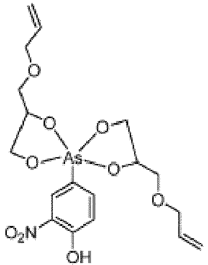
- A composition of matter having the chemical formula:

- A composition of matter having the chemical formula:

- A composition of matter having the chemical formula:

- A composition of matter having the chemical formula:

- A composition of matter having the chemical formula:

- A composition of matter having the chemical formula:

- A composition of matter having the chemical formula:

- A composition of matter having the chemical formula:

- A composition of matter having the chemical formula:

Claims (15)
- A composition of matter comprising:


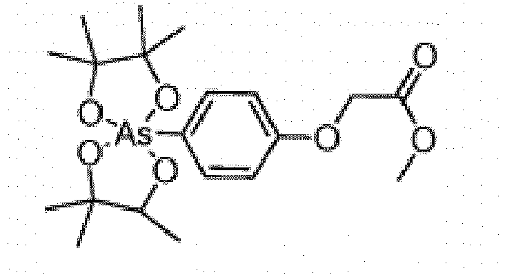


- The composition of matter of claim 1, wherein E1, E2, E3, or a combination thereof, comprises N, and N is further substituted by hydrogen, a hydrocarbyl group, or a silyl group; or wherein the E4, E5, E6, E7, or a combination thereof, include N, and N is further substituted by hydrogen, a hydrocarbyl group, or a silyl group; or wherein E8, E9, or a combination thereof, comprises N, and N is further substituted by hydrogen, a hydrocarbyl group, or a silyl group.
- A solution comprising:a solvent; andan arsenic-containing compound as described in any of claims 1 or 2;wherein the solution has a flashpoint that is at least equal to a minimum temperature capable of initiating a reaction between the solution and silicon within a duration of no greater than 2.5 hours.
- The solution of claim 3, wherein the solvent includes 4-hydroxy butanoic acid, a glycol ether (e.g., di-ethylene glycol di-butyl ether, tetra-ethylene glycol di-methyl ether (tetraglyme)), 4-formylmorpholine, phenylacetic acid, a C9 alcohol, a C10 alcohol, 3-nonanone, phenylpropyl ether, dimethylsulfoxide (DMSO), cyclooctanone, furfuryl acetone, isophorone, di-hexyl ether, 2-nonanone, phenyl propyl ether, hexyl benzene, mesitylene, N-methylpyrrolidone (NMP), an alkanolamine, acetonitrile, toluene, dioxane, tetrahydrofuran (THF), or combinations thereof.
- The solution of claim 5, wherein the flashpoint of the solution is within a range of 50 °C to 115°C.
- The solution of claim 5, wherein the solution includes the arsenic-containing compound within a range of 2 wt% to 11 wt% of the total weight of the solution.
- A substrate comprising:a surface having a plurality of silicon atoms; andan arsenic-containing compound as described in any of claims 1 or 2 covalently bonded to at least a portion of the plurality of the silicon atoms.
- The substrate of claim 7, wherein the substrate includes a plurality of layers of one or more arsenic-containing compounds covalently bonded to the at least a portion of the plurality of silicon atoms.
- A process, comprising:preparing a solution including a dopant and a solvent, the dopant including arsenic; andcontacting a substrate with the solution, wherein the solution has a flashpoint that is equal to or greater than a minimum temperature capable of causing attachment between at least a portion of atoms of the substrate and an arsenic-containing compound of the solution in a duration of no greater than 2.5 hours, wherein the dopant is selected from an arsenic-containing compound as described in any of claims 1 or 2.
- The process of claim 9, further comprising treating a surface of the substrate to produce a modified surface of the substrate.
- The process of claim 10, wherein the modified surface of the substrate includes at least a portion of a plurality of silicon atoms at the surface being bonded to hydrogen atoms; or wherein the modified surface of the substrate includes at least a portion of a plurality of silicon atoms at the surface being bonded to a respective linking moiety.
- The process of claim 9, wherein the arsenic-containing compound includes an organoarsenic compound, and contacting the substrate with the solution includes covalently bonding the organoarsenic compound to at least a portion of a plurality of silicon atoms at a surface of the substrate; or wherein the arsenic-containing compound includes an organoarsenic compound, and contacting the substrate with the solution includes covalently bonding the organoarsenic compound to at least a portion of the respective linking moieties.
- The process of claim 9, further comprising adding the dopant to the substrate; or further comprising adding the dopant to the substrate, and wherein adding the dopant to the substrate includes annealing the substrate.
- The process of claim 9, wherein the substrate includes silicon, germanium, or a combination thereof.
- The process of claim 9, wherein the arsenic-containing compound includes at least one of the compositions of matter of claims 1-2.
Applications Claiming Priority (2)
| Application Number | Priority Date | Filing Date | Title |
|---|---|---|---|
| US13/669,087 US8853438B2 (en) | 2012-11-05 | 2012-11-05 | Formulations of solutions and processes for forming a substrate including an arsenic dopant |
| PCT/US2013/068426 WO2014071352A2 (en) | 2012-11-05 | 2013-11-05 | Formulations of solutions and processes for forming a substrate including an arsenic dopant |
Publications (3)
| Publication Number | Publication Date |
|---|---|
| EP2915186A2 EP2915186A2 (en) | 2015-09-09 |
| EP2915186A4 EP2915186A4 (en) | 2016-05-25 |
| EP2915186B1 true EP2915186B1 (en) | 2020-10-28 |
Family
ID=50621584
Family Applications (1)
| Application Number | Title | Priority Date | Filing Date |
|---|---|---|---|
| EP13850348.7A Active EP2915186B1 (en) | 2012-11-05 | 2013-11-05 | Formulations of solutions and processes for forming a substrate including an arsenic dopant |
Country Status (7)
| Country | Link |
|---|---|
| US (1) | US8853438B2 (en) |
| EP (1) | EP2915186B1 (en) |
| JP (1) | JP6522507B2 (en) |
| KR (1) | KR102171051B1 (en) |
| CN (1) | CN104781909B (en) |
| TW (1) | TWI622676B (en) |
| WO (1) | WO2014071352A2 (en) |
Families Citing this family (6)
| Publication number | Priority date | Publication date | Assignee | Title |
|---|---|---|---|---|
| TWI539493B (en) | 2010-03-08 | 2016-06-21 | 黛納羅伊有限責任公司 | Method and composition for doping a germanium substrate having a molecular monolayer |
| US20150111372A1 (en) * | 2013-10-21 | 2015-04-23 | Sematech, Inc. | Phosphorus and arsenic doping of semiconductor materials |
| WO2015080985A1 (en) * | 2013-11-27 | 2015-06-04 | Entegris, Inc. | Dopant precursors for mono-layer doping |
| US20150325442A1 (en) * | 2014-05-07 | 2015-11-12 | Dynaloy, Llc | Formulations of Solutions and Processes for Forming a Substrate Including a Dopant |
| CN106558490A (en) | 2015-09-25 | 2017-04-05 | 中芯国际集成电路制造(上海)有限公司 | Semiconductor device and preparation method thereof |
| US11978633B2 (en) | 2019-05-08 | 2024-05-07 | Consiglio Nazionale Delle Ricerche | Molecular doping |
Citations (1)
| Publication number | Priority date | Publication date | Assignee | Title |
|---|---|---|---|---|
| WO2012044978A2 (en) * | 2010-10-01 | 2012-04-05 | Applied Materials, Inc. | High efficiency solar cell device with gallium arsenide absorber layer |
Family Cites Families (25)
| Publication number | Priority date | Publication date | Assignee | Title |
|---|---|---|---|---|
| JPS5368165A (en) * | 1976-11-30 | 1978-06-17 | Nec Corp | Production of semiconductor device |
| US4490192A (en) | 1983-06-08 | 1984-12-25 | Allied Corporation | Stable suspensions of boron, phosphorus, antimony and arsenic dopants |
| JPH03161924A (en) * | 1989-11-20 | 1991-07-11 | Sony Corp | Manufacture of semiconductor device |
| US5527872A (en) | 1990-09-14 | 1996-06-18 | At&T Global Information Solutions Company | Electronic device with a spin-on glass dielectric layer |
| JPH06291076A (en) * | 1993-03-31 | 1994-10-18 | Sony Corp | Joint structure and manufacturing method thereof |
| KR100223268B1 (en) * | 1996-06-25 | 1999-10-15 | 김영환 | Impurity ion implantation method of semiconductor device |
| DE19910816A1 (en) | 1999-03-11 | 2000-10-05 | Merck Patent Gmbh | Doping pastes for producing p, p + and n, n + regions in semiconductors |
| WO2001014250A2 (en) | 1999-08-23 | 2001-03-01 | University Of Hawaii | Synthesis of silicon nanoparticles and metal-centered silicon nanoparticles and applications thereof |
| US6323137B1 (en) | 2000-03-03 | 2001-11-27 | Promos Technologies | Method for forming an arsenic doped dielectric layer |
| US7084080B2 (en) | 2001-03-30 | 2006-08-01 | Advanced Technology Materials, Inc. | Silicon source reagent compositions, and method of making and using same for microelectronic device structure |
| US7064087B1 (en) | 2001-11-15 | 2006-06-20 | Novellus Systems, Inc. | Phosphorous-doped silicon dioxide process to customize contact etch profiles |
| US6911293B2 (en) | 2002-04-11 | 2005-06-28 | Clariant Finance (Bvi) Limited | Photoresist compositions comprising acetals and ketals as solvents |
| JP2005123431A (en) | 2003-10-17 | 2005-05-12 | Sanken Electric Co Ltd | Liquid impurity source material and method for manufacturing semiconductor device by using same |
| CH697007A5 (en) | 2004-05-03 | 2008-03-14 | Solaronix Sa | Method for producing a chalcopyrite compound thin layer. |
| CN101595115B (en) * | 2006-11-01 | 2012-07-18 | 新南部创新有限公司 | Organo-arsenic oxide compounds and uses thereof |
| US8586459B2 (en) | 2006-11-06 | 2013-11-19 | Semequip, Inc. | Ion implantation with molecular ions containing phosphorus and arsenic |
| JP5357442B2 (en) | 2008-04-09 | 2013-12-04 | 東京応化工業株式会社 | Inkjet diffusing agent composition, electrode using the composition, and method for producing solar cell |
| US20090286349A1 (en) | 2008-05-13 | 2009-11-19 | Georgia Tech Research Corporation | Solar cell spin-on based process for simultaneous diffusion and passivation |
| JP5815215B2 (en) | 2009-08-27 | 2015-11-17 | 東京応化工業株式会社 | Diffusion agent composition and method for forming impurity diffusion layer |
| KR20110024639A (en) * | 2009-09-02 | 2011-03-09 | 엘지이노텍 주식회사 | Dopant Diffusion Solution, and Uses thereof |
| US7955989B2 (en) | 2009-09-24 | 2011-06-07 | Rohm And Haas Electronic Materials Llc | Texturing semiconductor substrates |
| US8691675B2 (en) | 2009-11-25 | 2014-04-08 | International Business Machines Corporation | Vapor phase deposition processes for doping silicon |
| US8354333B2 (en) | 2010-02-03 | 2013-01-15 | International Business Machines Corporation | Patterned doping of semiconductor substrates using photosensitive monolayers |
| TWI539493B (en) | 2010-03-08 | 2016-06-21 | 黛納羅伊有限責任公司 | Method and composition for doping a germanium substrate having a molecular monolayer |
| JP6006040B2 (en) * | 2012-08-27 | 2016-10-12 | 株式会社Screenホールディングス | Substrate processing equipment |
-
2012
- 2012-11-05 US US13/669,087 patent/US8853438B2/en active Active
-
2013
- 2013-11-05 EP EP13850348.7A patent/EP2915186B1/en active Active
- 2013-11-05 TW TW102140213A patent/TWI622676B/en not_active IP Right Cessation
- 2013-11-05 CN CN201380057792.XA patent/CN104781909B/en not_active Expired - Fee Related
- 2013-11-05 WO PCT/US2013/068426 patent/WO2014071352A2/en not_active Ceased
- 2013-11-05 JP JP2015541844A patent/JP6522507B2/en not_active Expired - Fee Related
- 2013-11-05 KR KR1020157014719A patent/KR102171051B1/en not_active Expired - Fee Related
Patent Citations (1)
| Publication number | Priority date | Publication date | Assignee | Title |
|---|---|---|---|---|
| WO2012044978A2 (en) * | 2010-10-01 | 2012-04-05 | Applied Materials, Inc. | High efficiency solar cell device with gallium arsenide absorber layer |
Also Published As
| Publication number | Publication date |
|---|---|
| JP2016514359A (en) | 2016-05-19 |
| JP6522507B2 (en) | 2019-05-29 |
| CN104781909B (en) | 2019-02-05 |
| TWI622676B (en) | 2018-05-01 |
| US20140124896A1 (en) | 2014-05-08 |
| WO2014071352A2 (en) | 2014-05-08 |
| US8853438B2 (en) | 2014-10-07 |
| EP2915186A4 (en) | 2016-05-25 |
| TW201432104A (en) | 2014-08-16 |
| CN104781909A (en) | 2015-07-15 |
| KR20150079958A (en) | 2015-07-08 |
| EP2915186A2 (en) | 2015-09-09 |
| KR102171051B1 (en) | 2020-10-28 |
| WO2014071352A3 (en) | 2014-06-26 |
Similar Documents
| Publication | Publication Date | Title |
|---|---|---|
| US8853438B2 (en) | Formulations of solutions and processes for forming a substrate including an arsenic dopant | |
| JP2013084959A5 (en) | ||
| TWI539493B (en) | Method and composition for doping a germanium substrate having a molecular monolayer | |
| CN111971803A (en) | Polymerizable self-assembling monomers for atomic layer deposition | |
| TW202205425A (en) | Etching method and etching device of silicon oxide | |
| JP2004161601A5 (en) | ||
| US20110186969A1 (en) | Patterned doping of semiconductor substrates using photosensitive monolayers | |
| SG190068A1 (en) | Process for cleaning wafers | |
| US20170062203A1 (en) | Method of Preparing Liquid Chemical for Forming Protective Film | |
| TWI867126B (en) | Etching liquid, and method for manufacturing semiconductor device | |
| TW202407796A (en) | Method of treating base material and manufacturing base material | |
| TWI900737B (en) | Surface treatment composition and method for manufacturing wafer | |
| JP3522940B2 (en) | Boron diffusion coating solution | |
| WO2015171386A1 (en) | Formulations of solutions and processes for forming a substrate including a dopant | |
| JP4733786B2 (en) | How to mount parts | |
| EP4155376A1 (en) | Surface treatment method for semiconductor substrate, and surface treatment agent composition | |
| JP2023066405A (en) | Silicon etchant containing aromatic aldehyde | |
| KR20160114517A (en) | Process for preparing chemical liquid of silylating agent and surface treatment method | |
| TWI704153B (en) | Water-repellent protective film forming agent, chemical liquid for forming water-repellent protective film, and surface treatment method of wafer | |
| TW202200756A (en) | Semiconductor processing liquid and method for processing substrate | |
| KR20190127051A (en) | Silane compound, insulation layer etchant composition comprising the same and method of forming pattern using the same | |
| JP2016530225A (en) | Method for producing indium alkoxide compound, indium alkoxide compound that can be produced according to the method, and use of the compound | |
| TW202347482A (en) | Surface treatment composition, and wafer manufacturing method | |
| EP4155375A1 (en) | Surface treatment method for semiconductor substrates, and surface treatment agent composition | |
| TW202540133A (en) | Electron-withdrawing functional groups on si-chalcogen precursors |
Legal Events
| Date | Code | Title | Description |
|---|---|---|---|
| PUAI | Public reference made under article 153(3) epc to a published international application that has entered the european phase |
Free format text: ORIGINAL CODE: 0009012 |
|
| 17P | Request for examination filed |
Effective date: 20150602 |
|
| AK | Designated contracting states |
Kind code of ref document: A2 Designated state(s): AL AT BE BG CH CY CZ DE DK EE ES FI FR GB GR HR HU IE IS IT LI LT LU LV MC MK MT NL NO PL PT RO RS SE SI SK SM TR |
|
| AX | Request for extension of the european patent |
Extension state: BA ME |
|
| DAX | Request for extension of the european patent (deleted) | ||
| A4 | Supplementary search report drawn up and despatched |
Effective date: 20160421 |
|
| RIC1 | Information provided on ipc code assigned before grant |
Ipc: H01L 21/228 20060101AFI20160415BHEP |
|
| STAA | Information on the status of an ep patent application or granted ep patent |
Free format text: STATUS: EXAMINATION IS IN PROGRESS |
|
| 17Q | First examination report despatched |
Effective date: 20180221 |
|
| RAP1 | Party data changed (applicant data changed or rights of an application transferred) |
Owner name: VERSUM MATERIALS US, LLC |
|
| GRAP | Despatch of communication of intention to grant a patent |
Free format text: ORIGINAL CODE: EPIDOSNIGR1 |
|
| STAA | Information on the status of an ep patent application or granted ep patent |
Free format text: STATUS: GRANT OF PATENT IS INTENDED |
|
| INTG | Intention to grant announced |
Effective date: 20200515 |
|
| GRAS | Grant fee paid |
Free format text: ORIGINAL CODE: EPIDOSNIGR3 |
|
| GRAA | (expected) grant |
Free format text: ORIGINAL CODE: 0009210 |
|
| STAA | Information on the status of an ep patent application or granted ep patent |
Free format text: STATUS: THE PATENT HAS BEEN GRANTED |
|
| AK | Designated contracting states |
Kind code of ref document: B1 Designated state(s): AL AT BE BG CH CY CZ DE DK EE ES FI FR GB GR HR HU IE IS IT LI LT LU LV MC MK MT NL NO PL PT RO RS SE SI SK SM TR |
|
| REG | Reference to a national code |
Ref country code: GB Ref legal event code: FG4D |
|
| REG | Reference to a national code |
Ref country code: CH Ref legal event code: EP |
|
| REG | Reference to a national code |
Ref country code: DE Ref legal event code: R096 Ref document number: 602013073672 Country of ref document: DE |
|
| REG | Reference to a national code |
Ref country code: AT Ref legal event code: REF Ref document number: 1329067 Country of ref document: AT Kind code of ref document: T Effective date: 20201115 |
|
| REG | Reference to a national code |
Ref country code: IE Ref legal event code: FG4D |
|
| REG | Reference to a national code |
Ref country code: AT Ref legal event code: MK05 Ref document number: 1329067 Country of ref document: AT Kind code of ref document: T Effective date: 20201028 |
|
| REG | Reference to a national code |
Ref country code: NL Ref legal event code: MP Effective date: 20201028 |
|
| PG25 | Lapsed in a contracting state [announced via postgrant information from national office to epo] |
Ref country code: GR Free format text: LAPSE BECAUSE OF FAILURE TO SUBMIT A TRANSLATION OF THE DESCRIPTION OR TO PAY THE FEE WITHIN THE PRESCRIBED TIME-LIMIT Effective date: 20210129 Ref country code: FI Free format text: LAPSE BECAUSE OF FAILURE TO SUBMIT A TRANSLATION OF THE DESCRIPTION OR TO PAY THE FEE WITHIN THE PRESCRIBED TIME-LIMIT Effective date: 20201028 Ref country code: RS Free format text: LAPSE BECAUSE OF FAILURE TO SUBMIT A TRANSLATION OF THE DESCRIPTION OR TO PAY THE FEE WITHIN THE PRESCRIBED TIME-LIMIT Effective date: 20201028 Ref country code: NO Free format text: LAPSE BECAUSE OF FAILURE TO SUBMIT A TRANSLATION OF THE DESCRIPTION OR TO PAY THE FEE WITHIN THE PRESCRIBED TIME-LIMIT Effective date: 20210128 Ref country code: NL Free format text: LAPSE BECAUSE OF FAILURE TO SUBMIT A TRANSLATION OF THE DESCRIPTION OR TO PAY THE FEE WITHIN THE PRESCRIBED TIME-LIMIT Effective date: 20201028 Ref country code: PT Free format text: LAPSE BECAUSE OF FAILURE TO SUBMIT A TRANSLATION OF THE DESCRIPTION OR TO PAY THE FEE WITHIN THE PRESCRIBED TIME-LIMIT Effective date: 20210301 |
|
| REG | Reference to a national code |
Ref country code: LT Ref legal event code: MG4D |
|
| PG25 | Lapsed in a contracting state [announced via postgrant information from national office to epo] |
Ref country code: ES Free format text: LAPSE BECAUSE OF FAILURE TO SUBMIT A TRANSLATION OF THE DESCRIPTION OR TO PAY THE FEE WITHIN THE PRESCRIBED TIME-LIMIT Effective date: 20201028 Ref country code: AT Free format text: LAPSE BECAUSE OF FAILURE TO SUBMIT A TRANSLATION OF THE DESCRIPTION OR TO PAY THE FEE WITHIN THE PRESCRIBED TIME-LIMIT Effective date: 20201028 Ref country code: BG Free format text: LAPSE BECAUSE OF FAILURE TO SUBMIT A TRANSLATION OF THE DESCRIPTION OR TO PAY THE FEE WITHIN THE PRESCRIBED TIME-LIMIT Effective date: 20210128 Ref country code: PL Free format text: LAPSE BECAUSE OF FAILURE TO SUBMIT A TRANSLATION OF THE DESCRIPTION OR TO PAY THE FEE WITHIN THE PRESCRIBED TIME-LIMIT Effective date: 20201028 Ref country code: LV Free format text: LAPSE BECAUSE OF FAILURE TO SUBMIT A TRANSLATION OF THE DESCRIPTION OR TO PAY THE FEE WITHIN THE PRESCRIBED TIME-LIMIT Effective date: 20201028 Ref country code: IS Free format text: LAPSE BECAUSE OF FAILURE TO SUBMIT A TRANSLATION OF THE DESCRIPTION OR TO PAY THE FEE WITHIN THE PRESCRIBED TIME-LIMIT Effective date: 20210228 Ref country code: SE Free format text: LAPSE BECAUSE OF FAILURE TO SUBMIT A TRANSLATION OF THE DESCRIPTION OR TO PAY THE FEE WITHIN THE PRESCRIBED TIME-LIMIT Effective date: 20201028 |
|
| PG25 | Lapsed in a contracting state [announced via postgrant information from national office to epo] |
Ref country code: HR Free format text: LAPSE BECAUSE OF FAILURE TO SUBMIT A TRANSLATION OF THE DESCRIPTION OR TO PAY THE FEE WITHIN THE PRESCRIBED TIME-LIMIT Effective date: 20201028 |
|
| REG | Reference to a national code |
Ref country code: CH Ref legal event code: PL |
|
| REG | Reference to a national code |
Ref country code: DE Ref legal event code: R097 Ref document number: 602013073672 Country of ref document: DE |
|
| PG25 | Lapsed in a contracting state [announced via postgrant information from national office to epo] |
Ref country code: SM Free format text: LAPSE BECAUSE OF FAILURE TO SUBMIT A TRANSLATION OF THE DESCRIPTION OR TO PAY THE FEE WITHIN THE PRESCRIBED TIME-LIMIT Effective date: 20201028 Ref country code: EE Free format text: LAPSE BECAUSE OF FAILURE TO SUBMIT A TRANSLATION OF THE DESCRIPTION OR TO PAY THE FEE WITHIN THE PRESCRIBED TIME-LIMIT Effective date: 20201028 Ref country code: CZ Free format text: LAPSE BECAUSE OF FAILURE TO SUBMIT A TRANSLATION OF THE DESCRIPTION OR TO PAY THE FEE WITHIN THE PRESCRIBED TIME-LIMIT Effective date: 20201028 Ref country code: MC Free format text: LAPSE BECAUSE OF FAILURE TO SUBMIT A TRANSLATION OF THE DESCRIPTION OR TO PAY THE FEE WITHIN THE PRESCRIBED TIME-LIMIT Effective date: 20201028 Ref country code: LT Free format text: LAPSE BECAUSE OF FAILURE TO SUBMIT A TRANSLATION OF THE DESCRIPTION OR TO PAY THE FEE WITHIN THE PRESCRIBED TIME-LIMIT Effective date: 20201028 Ref country code: LU Free format text: LAPSE BECAUSE OF NON-PAYMENT OF DUE FEES Effective date: 20201105 Ref country code: SK Free format text: LAPSE BECAUSE OF FAILURE TO SUBMIT A TRANSLATION OF THE DESCRIPTION OR TO PAY THE FEE WITHIN THE PRESCRIBED TIME-LIMIT Effective date: 20201028 Ref country code: RO Free format text: LAPSE BECAUSE OF FAILURE TO SUBMIT A TRANSLATION OF THE DESCRIPTION OR TO PAY THE FEE WITHIN THE PRESCRIBED TIME-LIMIT Effective date: 20201028 |
|
| REG | Reference to a national code |
Ref country code: BE Ref legal event code: MM Effective date: 20201130 |
|
| PG25 | Lapsed in a contracting state [announced via postgrant information from national office to epo] |
Ref country code: DK Free format text: LAPSE BECAUSE OF FAILURE TO SUBMIT A TRANSLATION OF THE DESCRIPTION OR TO PAY THE FEE WITHIN THE PRESCRIBED TIME-LIMIT Effective date: 20201028 Ref country code: CH Free format text: LAPSE BECAUSE OF NON-PAYMENT OF DUE FEES Effective date: 20201130 Ref country code: LI Free format text: LAPSE BECAUSE OF NON-PAYMENT OF DUE FEES Effective date: 20201130 |
|
| PLBE | No opposition filed within time limit |
Free format text: ORIGINAL CODE: 0009261 |
|
| STAA | Information on the status of an ep patent application or granted ep patent |
Free format text: STATUS: NO OPPOSITION FILED WITHIN TIME LIMIT |
|
| GBPC | Gb: european patent ceased through non-payment of renewal fee |
Effective date: 20210128 |
|
| 26N | No opposition filed |
Effective date: 20210729 |
|
| PG25 | Lapsed in a contracting state [announced via postgrant information from national office to epo] |
Ref country code: IT Free format text: LAPSE BECAUSE OF FAILURE TO SUBMIT A TRANSLATION OF THE DESCRIPTION OR TO PAY THE FEE WITHIN THE PRESCRIBED TIME-LIMIT Effective date: 20201028 Ref country code: AL Free format text: LAPSE BECAUSE OF FAILURE TO SUBMIT A TRANSLATION OF THE DESCRIPTION OR TO PAY THE FEE WITHIN THE PRESCRIBED TIME-LIMIT Effective date: 20201028 |
|
| PGFP | Annual fee paid to national office [announced via postgrant information from national office to epo] |
Ref country code: FR Payment date: 20210930 Year of fee payment: 9 |
|
| PG25 | Lapsed in a contracting state [announced via postgrant information from national office to epo] |
Ref country code: GB Free format text: LAPSE BECAUSE OF NON-PAYMENT OF DUE FEES Effective date: 20210128 Ref country code: SI Free format text: LAPSE BECAUSE OF FAILURE TO SUBMIT A TRANSLATION OF THE DESCRIPTION OR TO PAY THE FEE WITHIN THE PRESCRIBED TIME-LIMIT Effective date: 20201028 |
|
| PGFP | Annual fee paid to national office [announced via postgrant information from national office to epo] |
Ref country code: IE Payment date: 20211012 Year of fee payment: 9 Ref country code: DE Payment date: 20210923 Year of fee payment: 9 |
|
| PG25 | Lapsed in a contracting state [announced via postgrant information from national office to epo] |
Ref country code: IS Free format text: LAPSE BECAUSE OF FAILURE TO SUBMIT A TRANSLATION OF THE DESCRIPTION OR TO PAY THE FEE WITHIN THE PRESCRIBED TIME-LIMIT Effective date: 20210228 Ref country code: TR Free format text: LAPSE BECAUSE OF FAILURE TO SUBMIT A TRANSLATION OF THE DESCRIPTION OR TO PAY THE FEE WITHIN THE PRESCRIBED TIME-LIMIT Effective date: 20201028 Ref country code: MT Free format text: LAPSE BECAUSE OF FAILURE TO SUBMIT A TRANSLATION OF THE DESCRIPTION OR TO PAY THE FEE WITHIN THE PRESCRIBED TIME-LIMIT Effective date: 20201028 Ref country code: CY Free format text: LAPSE BECAUSE OF FAILURE TO SUBMIT A TRANSLATION OF THE DESCRIPTION OR TO PAY THE FEE WITHIN THE PRESCRIBED TIME-LIMIT Effective date: 20201028 |
|
| PG25 | Lapsed in a contracting state [announced via postgrant information from national office to epo] |
Ref country code: MK Free format text: LAPSE BECAUSE OF FAILURE TO SUBMIT A TRANSLATION OF THE DESCRIPTION OR TO PAY THE FEE WITHIN THE PRESCRIBED TIME-LIMIT Effective date: 20201028 |
|
| PG25 | Lapsed in a contracting state [announced via postgrant information from national office to epo] |
Ref country code: BE Free format text: LAPSE BECAUSE OF NON-PAYMENT OF DUE FEES Effective date: 20201130 |
|
| REG | Reference to a national code |
Ref country code: DE Ref legal event code: R119 Ref document number: 602013073672 Country of ref document: DE |
|
| P01 | Opt-out of the competence of the unified patent court (upc) registered |
Effective date: 20230602 |
|
| PG25 | Lapsed in a contracting state [announced via postgrant information from national office to epo] |
Ref country code: IE Free format text: LAPSE BECAUSE OF NON-PAYMENT OF DUE FEES Effective date: 20221105 Ref country code: DE Free format text: LAPSE BECAUSE OF NON-PAYMENT OF DUE FEES Effective date: 20230601 |
|
| PG25 | Lapsed in a contracting state [announced via postgrant information from national office to epo] |
Ref country code: FR Free format text: LAPSE BECAUSE OF NON-PAYMENT OF DUE FEES Effective date: 20221130 |