EP2914455B9 - Schaltungsanordnung umfassend aufnehmeranordnung und variable kompensationsanordnung, und verfahren - Google Patents
Schaltungsanordnung umfassend aufnehmeranordnung und variable kompensationsanordnung, und verfahren Download PDFInfo
- Publication number
- EP2914455B9 EP2914455B9 EP13783932.0A EP13783932A EP2914455B9 EP 2914455 B9 EP2914455 B9 EP 2914455B9 EP 13783932 A EP13783932 A EP 13783932A EP 2914455 B9 EP2914455 B9 EP 2914455B9
- Authority
- EP
- European Patent Office
- Prior art keywords
- switching element
- arrangement
- circuit arrangement
- switching
- variable compensating
- Prior art date
- Legal status (The legal status is an assumption and is not a legal conclusion. Google has not performed a legal analysis and makes no representation as to the accuracy of the status listed.)
- Active
Links
Images

Classifications
-
- B—PERFORMING OPERATIONS; TRANSPORTING
- B60—VEHICLES IN GENERAL
- B60L—PROPULSION OF ELECTRICALLY-PROPELLED VEHICLES; SUPPLYING ELECTRIC POWER FOR AUXILIARY EQUIPMENT OF ELECTRICALLY-PROPELLED VEHICLES; ELECTRODYNAMIC BRAKE SYSTEMS FOR VEHICLES IN GENERAL; MAGNETIC SUSPENSION OR LEVITATION FOR VEHICLES; MONITORING OPERATING VARIABLES OF ELECTRICALLY-PROPELLED VEHICLES; ELECTRIC SAFETY DEVICES FOR ELECTRICALLY-PROPELLED VEHICLES
- B60L53/00—Methods of charging batteries, specially adapted for electric vehicles; Charging stations or on-board charging equipment therefor; Exchange of energy storage elements in electric vehicles
- B60L53/10—Methods of charging batteries, specially adapted for electric vehicles; Charging stations or on-board charging equipment therefor; Exchange of energy storage elements in electric vehicles characterised by the energy transfer between the charging station and the vehicle
- B60L53/12—Inductive energy transfer
-
- B—PERFORMING OPERATIONS; TRANSPORTING
- B60—VEHICLES IN GENERAL
- B60L—PROPULSION OF ELECTRICALLY-PROPELLED VEHICLES; SUPPLYING ELECTRIC POWER FOR AUXILIARY EQUIPMENT OF ELECTRICALLY-PROPELLED VEHICLES; ELECTRODYNAMIC BRAKE SYSTEMS FOR VEHICLES IN GENERAL; MAGNETIC SUSPENSION OR LEVITATION FOR VEHICLES; MONITORING OPERATING VARIABLES OF ELECTRICALLY-PROPELLED VEHICLES; ELECTRIC SAFETY DEVICES FOR ELECTRICALLY-PROPELLED VEHICLES
- B60L53/00—Methods of charging batteries, specially adapted for electric vehicles; Charging stations or on-board charging equipment therefor; Exchange of energy storage elements in electric vehicles
- B60L53/30—Constructional details of charging stations
- B60L53/35—Means for automatic or assisted adjustment of the relative position of charging devices and vehicles
- B60L53/38—Means for automatic or assisted adjustment of the relative position of charging devices and vehicles specially adapted for charging by inductive energy transfer
-
- B—PERFORMING OPERATIONS; TRANSPORTING
- B60—VEHICLES IN GENERAL
- B60L—PROPULSION OF ELECTRICALLY-PROPELLED VEHICLES; SUPPLYING ELECTRIC POWER FOR AUXILIARY EQUIPMENT OF ELECTRICALLY-PROPELLED VEHICLES; ELECTRODYNAMIC BRAKE SYSTEMS FOR VEHICLES IN GENERAL; MAGNETIC SUSPENSION OR LEVITATION FOR VEHICLES; MONITORING OPERATING VARIABLES OF ELECTRICALLY-PROPELLED VEHICLES; ELECTRIC SAFETY DEVICES FOR ELECTRICALLY-PROPELLED VEHICLES
- B60L53/00—Methods of charging batteries, specially adapted for electric vehicles; Charging stations or on-board charging equipment therefor; Exchange of energy storage elements in electric vehicles
- B60L53/30—Constructional details of charging stations
- B60L53/35—Means for automatic or assisted adjustment of the relative position of charging devices and vehicles
- B60L53/38—Means for automatic or assisted adjustment of the relative position of charging devices and vehicles specially adapted for charging by inductive energy transfer
- B60L53/39—Means for automatic or assisted adjustment of the relative position of charging devices and vehicles specially adapted for charging by inductive energy transfer with position-responsive activation of primary coils
-
- B—PERFORMING OPERATIONS; TRANSPORTING
- B60—VEHICLES IN GENERAL
- B60L—PROPULSION OF ELECTRICALLY-PROPELLED VEHICLES; SUPPLYING ELECTRIC POWER FOR AUXILIARY EQUIPMENT OF ELECTRICALLY-PROPELLED VEHICLES; ELECTRODYNAMIC BRAKE SYSTEMS FOR VEHICLES IN GENERAL; MAGNETIC SUSPENSION OR LEVITATION FOR VEHICLES; MONITORING OPERATING VARIABLES OF ELECTRICALLY-PROPELLED VEHICLES; ELECTRIC SAFETY DEVICES FOR ELECTRICALLY-PROPELLED VEHICLES
- B60L9/00—Electric propulsion with power supply external to the vehicle
-
- H—ELECTRICITY
- H01—ELECTRIC ELEMENTS
- H01F—MAGNETS; INDUCTANCES; TRANSFORMERS; SELECTION OF MATERIALS FOR THEIR MAGNETIC PROPERTIES
- H01F38/00—Adaptations of transformers or inductances for specific applications or functions
- H01F38/14—Inductive couplings
-
- H—ELECTRICITY
- H02—GENERATION; CONVERSION OR DISTRIBUTION OF ELECTRIC POWER
- H02J—ELECTRIC POWER NETWORKS; CIRCUIT ARRANGEMENTS OR SYSTEMS FOR SUPPLYING OR DISTRIBUTING ELECTRIC POWER; SYSTEMS FOR STORING ELECTRIC ENERGY
- H02J50/00—Circuit arrangements or systems for wireless supply or distribution of electric power
- H02J50/10—Circuit arrangements or systems for wireless supply or distribution of electric power using inductive coupling
- H02J50/12—Circuit arrangements or systems for wireless supply or distribution of electric power using inductive coupling of the resonant type
-
- H—ELECTRICITY
- H02—GENERATION; CONVERSION OR DISTRIBUTION OF ELECTRIC POWER
- H02J—ELECTRIC POWER NETWORKS; CIRCUIT ARRANGEMENTS OR SYSTEMS FOR SUPPLYING OR DISTRIBUTING ELECTRIC POWER; SYSTEMS FOR STORING ELECTRIC ENERGY
- H02J50/00—Circuit arrangements or systems for wireless supply or distribution of electric power
- H02J50/40—Circuit arrangements or systems for wireless supply or distribution of electric power using two or more transmitting or receiving devices
- H02J50/402—Circuit arrangements or systems for wireless supply or distribution of electric power using two or more transmitting or receiving devices the two or more transmitting or the two or more receiving devices being integrated in the same unit, e.g. power mats with several coils or antennas with several sub-antennas
-
- H—ELECTRICITY
- H02—GENERATION; CONVERSION OR DISTRIBUTION OF ELECTRIC POWER
- H02J—ELECTRIC POWER NETWORKS; CIRCUIT ARRANGEMENTS OR SYSTEMS FOR SUPPLYING OR DISTRIBUTING ELECTRIC POWER; SYSTEMS FOR STORING ELECTRIC ENERGY
- H02J50/00—Circuit arrangements or systems for wireless supply or distribution of electric power
- H02J50/70—Circuit arrangements or systems for wireless supply or distribution of electric power involving the reduction of electric, magnetic or electromagnetic leakage fields
-
- H—ELECTRICITY
- H02—GENERATION; CONVERSION OR DISTRIBUTION OF ELECTRIC POWER
- H02J—ELECTRIC POWER NETWORKS; CIRCUIT ARRANGEMENTS OR SYSTEMS FOR SUPPLYING OR DISTRIBUTING ELECTRIC POWER; SYSTEMS FOR STORING ELECTRIC ENERGY
- H02J7/00—Circuit arrangements for charging or discharging batteries or for supplying loads from batteries
- H02J7/90—Regulation of charging or discharging current or voltage
- H02J7/933—Regulation of charging or discharging current or voltage the cycle being controlled or terminated in response to electric parameters
-
- H—ELECTRICITY
- H02—GENERATION; CONVERSION OR DISTRIBUTION OF ELECTRIC POWER
- H02M—APPARATUS FOR CONVERSION BETWEEN AC AND AC, BETWEEN AC AND DC, OR BETWEEN DC AND DC, AND FOR USE WITH MAINS OR SIMILAR POWER SUPPLY SYSTEMS; CONVERSION OF DC OR AC INPUT POWER INTO SURGE OUTPUT POWER; CONTROL OR REGULATION THEREOF
- H02M1/00—Details of apparatus for conversion
- H02M1/42—Circuits or arrangements for compensating for or adjusting power factor in converters or inverters
- H02M1/4208—Arrangements for improving power factor of AC input
- H02M1/4266—Arrangements for improving power factor of AC input using passive elements
-
- B—PERFORMING OPERATIONS; TRANSPORTING
- B60—VEHICLES IN GENERAL
- B60L—PROPULSION OF ELECTRICALLY-PROPELLED VEHICLES; SUPPLYING ELECTRIC POWER FOR AUXILIARY EQUIPMENT OF ELECTRICALLY-PROPELLED VEHICLES; ELECTRODYNAMIC BRAKE SYSTEMS FOR VEHICLES IN GENERAL; MAGNETIC SUSPENSION OR LEVITATION FOR VEHICLES; MONITORING OPERATING VARIABLES OF ELECTRICALLY-PROPELLED VEHICLES; ELECTRIC SAFETY DEVICES FOR ELECTRICALLY-PROPELLED VEHICLES
- B60L2200/00—Type of vehicles
- B60L2200/26—Rail vehicles
-
- B—PERFORMING OPERATIONS; TRANSPORTING
- B60—VEHICLES IN GENERAL
- B60L—PROPULSION OF ELECTRICALLY-PROPELLED VEHICLES; SUPPLYING ELECTRIC POWER FOR AUXILIARY EQUIPMENT OF ELECTRICALLY-PROPELLED VEHICLES; ELECTRODYNAMIC BRAKE SYSTEMS FOR VEHICLES IN GENERAL; MAGNETIC SUSPENSION OR LEVITATION FOR VEHICLES; MONITORING OPERATING VARIABLES OF ELECTRICALLY-PROPELLED VEHICLES; ELECTRIC SAFETY DEVICES FOR ELECTRICALLY-PROPELLED VEHICLES
- B60L2200/00—Type of vehicles
- B60L2200/30—Trolleys
-
- B—PERFORMING OPERATIONS; TRANSPORTING
- B60—VEHICLES IN GENERAL
- B60L—PROPULSION OF ELECTRICALLY-PROPELLED VEHICLES; SUPPLYING ELECTRIC POWER FOR AUXILIARY EQUIPMENT OF ELECTRICALLY-PROPELLED VEHICLES; ELECTRODYNAMIC BRAKE SYSTEMS FOR VEHICLES IN GENERAL; MAGNETIC SUSPENSION OR LEVITATION FOR VEHICLES; MONITORING OPERATING VARIABLES OF ELECTRICALLY-PROPELLED VEHICLES; ELECTRIC SAFETY DEVICES FOR ELECTRICALLY-PROPELLED VEHICLES
- B60L5/00—Current collectors for power supply lines of electrically-propelled vehicles
- B60L5/005—Current collectors for power supply lines of electrically-propelled vehicles without mechanical contact between the collector and the power supply line
-
- H—ELECTRICITY
- H02—GENERATION; CONVERSION OR DISTRIBUTION OF ELECTRIC POWER
- H02J—ELECTRIC POWER NETWORKS; CIRCUIT ARRANGEMENTS OR SYSTEMS FOR SUPPLYING OR DISTRIBUTING ELECTRIC POWER; SYSTEMS FOR STORING ELECTRIC ENERGY
- H02J2105/00—Networks for supplying or distributing electric power characterised by their spatial reach or by the load
- H02J2105/30—Networks for supplying or distributing electric power characterised by their spatial reach or by the load the load networks being external to vehicles, i.e. exchanging power with vehicles
- H02J2105/33—Networks for supplying or distributing electric power characterised by their spatial reach or by the load the load networks being external to vehicles, i.e. exchanging power with vehicles exchanging power with road vehicles
- H02J2105/37—Networks for supplying or distributing electric power characterised by their spatial reach or by the load the load networks being external to vehicles, i.e. exchanging power with vehicles exchanging power with road vehicles exchanging power with electric vehicles [EV] or with hybrid electric vehicles [HEV]
-
- Y—GENERAL TAGGING OF NEW TECHNOLOGICAL DEVELOPMENTS; GENERAL TAGGING OF CROSS-SECTIONAL TECHNOLOGIES SPANNING OVER SEVERAL SECTIONS OF THE IPC; TECHNICAL SUBJECTS COVERED BY FORMER USPC CROSS-REFERENCE ART COLLECTIONS [XRACs] AND DIGESTS
- Y02—TECHNOLOGIES OR APPLICATIONS FOR MITIGATION OR ADAPTATION AGAINST CLIMATE CHANGE
- Y02T—CLIMATE CHANGE MITIGATION TECHNOLOGIES RELATED TO TRANSPORTATION
- Y02T10/00—Road transport of goods or passengers
- Y02T10/60—Other road transportation technologies with climate change mitigation effect
- Y02T10/70—Energy storage systems for electromobility, e.g. batteries
-
- Y—GENERAL TAGGING OF NEW TECHNOLOGICAL DEVELOPMENTS; GENERAL TAGGING OF CROSS-SECTIONAL TECHNOLOGIES SPANNING OVER SEVERAL SECTIONS OF THE IPC; TECHNICAL SUBJECTS COVERED BY FORMER USPC CROSS-REFERENCE ART COLLECTIONS [XRACs] AND DIGESTS
- Y02—TECHNOLOGIES OR APPLICATIONS FOR MITIGATION OR ADAPTATION AGAINST CLIMATE CHANGE
- Y02T—CLIMATE CHANGE MITIGATION TECHNOLOGIES RELATED TO TRANSPORTATION
- Y02T10/00—Road transport of goods or passengers
- Y02T10/60—Other road transportation technologies with climate change mitigation effect
- Y02T10/7072—Electromobility specific charging systems or methods for batteries, ultracapacitors, supercapacitors or double-layer capacitors
-
- Y—GENERAL TAGGING OF NEW TECHNOLOGICAL DEVELOPMENTS; GENERAL TAGGING OF CROSS-SECTIONAL TECHNOLOGIES SPANNING OVER SEVERAL SECTIONS OF THE IPC; TECHNICAL SUBJECTS COVERED BY FORMER USPC CROSS-REFERENCE ART COLLECTIONS [XRACs] AND DIGESTS
- Y02—TECHNOLOGIES OR APPLICATIONS FOR MITIGATION OR ADAPTATION AGAINST CLIMATE CHANGE
- Y02T—CLIMATE CHANGE MITIGATION TECHNOLOGIES RELATED TO TRANSPORTATION
- Y02T90/00—Enabling technologies or technologies with a potential or indirect contribution to GHG emissions mitigation
- Y02T90/10—Technologies relating to charging of electric vehicles
- Y02T90/12—Electric charging stations
-
- Y—GENERAL TAGGING OF NEW TECHNOLOGICAL DEVELOPMENTS; GENERAL TAGGING OF CROSS-SECTIONAL TECHNOLOGIES SPANNING OVER SEVERAL SECTIONS OF THE IPC; TECHNICAL SUBJECTS COVERED BY FORMER USPC CROSS-REFERENCE ART COLLECTIONS [XRACs] AND DIGESTS
- Y02—TECHNOLOGIES OR APPLICATIONS FOR MITIGATION OR ADAPTATION AGAINST CLIMATE CHANGE
- Y02T—CLIMATE CHANGE MITIGATION TECHNOLOGIES RELATED TO TRANSPORTATION
- Y02T90/00—Enabling technologies or technologies with a potential or indirect contribution to GHG emissions mitigation
- Y02T90/10—Technologies relating to charging of electric vehicles
- Y02T90/14—Plug-in electric vehicles
Definitions
- the invention relates to a circuit arrangement of an electric vehicle, in particular a vehicle-sided circuit arrangement of a system for inductive power transfer to the vehicle. Furthermore, the invention relates to a method of operating the named circuit arrangement. Further, the invention relates to a method of manufacturing a circuit arrangement of an electric vehicle and to an electric vehicle.
- Electric vehicles in particular a track-bound vehicle and/or a road automobile, can be operated by electric energy which is transferred by means of an inductive power transfer.
- a vehicle may comprise a circuit arrangement which can be a traction system or a part of a traction system of the vehicle comprising a receiving device adapted to receive an alternating electromagnetic field and to produce an alternating electric current by electromagnetic induction.
- a vehicle can comprise a rectifier adapted to convert an alternating current to a direct current.
- the direct current can be used to charge a traction battery or to operate an electric machine. In the latter case, the direct current can be converted into an alternating current by means of an inverter.
- the inductive power transfer is performed using two sets of e.g. three-phase windings.
- a first set is installed on the ground (primary windings) and can be fed by a wayside power converter (WPC).
- the second set of windings (secondary windings) is installed on the vehicle.
- the second set of windings can be attached underneath the vehicle, in the case of trams under some of its waggons.
- the second set of windings or, generally, the secondary side is often referred to as pick-up-arrangement or receiver.
- the first set of windings and the second set of windings form a high frequency transformer to transfer electric energy to the vehicle. This can be done in a static state (when there is no movement of the vehicle) and in a dynamic state (when the vehicle moves).
- the leakage inductance usually acts as a series inductance with each secondary winding. To be able to transfer high power levels, it is necessary to use an adequate capacitance in order to compensate the reactance of the inductors at an operating frequency of e.g. 20 kHz.
- the combination of the inductance(s), which can comprise the main or mutual inductance and/or the leakage inductance, and the capacitance(s), which can comprise the compensating capacitance forms a resonant circuit.
- a perfect impedance cancellation happens if impedance values of the inductance(s) and the capacitance(s) are chosen such that the natural resonance frequency of the resonant circuit is equal to the operating frequency. Such a resonant circuit is said to be tuned.
- a tolerance of a compensating capacitance can increase.
- configurations with magnetically permeable materials tend to drift in the relevant parameters. This may result in a detuning of the resonant circuit, wherein the changed resonant frequency does not correspond to the operating frequency any more.
- Such a detuning deviates the overall performance and power transfer capability of the inductive power transfer system.
- an impedance of the secondary side reflected to the primary side of the transformer can become capacitive. This can result in a leading current with respect to the voltage in the WPC which is highly unwanted because a leading current eliminates soft switching conditions of semiconductor switches and increases their power losses considerably. Under such operation conditions, a WPC can overheat and turn off which, in turn, interrupts the needed power transfer.
- US 5,207,304 B2 discloses a power pickup system for an electrically powered vehicle.
- the system comprises a pickup inductor connected to first and second nodes, a power receiving circuit coupled to said first and second nodes, a multiplicity of tuning capacitors, a branch selection means for selecting ones of said multiplicity of tuning capacitors to be coupled to said first and second nodes and for generating a selected signal for each selected tuning capacitor, and a multiplicity of switching circuits, each switching circuit selectively coupling a corresponding tuning capacitor to said first and second nodes.
- Each switching circuit includes a solid state switch and a trigger circuit coupled to said branch selection means and said solid state switch.
- Said trigger circuit senses the voltage across said solid state switch and, after receiving one said selection signal from said branch selection means that corresponds to said switching circuit, triggers closure of said solid state switch when said sensed voltage across said solid state switch is approximately zero.
- an output current of an inductive coupling system can be controlled by switching a tuning capacitance into or out of the control circuit.
- EP 2 345 553 A1 discloses a non contact electric power transfer device which includes: a self resonant coil; an induction coil capable of transmitting and receiving electric power to and from an induction coil capable of the self resonance coil through electromagnetic induction; and a bobbin that has at least one of the self resonant coil and the induction coil attached thereto, and has an accommodation chamber defined therein and capable of accommodating a device therein.
- WO 94/24622 A1 discloses a series compensation system provided for compensating a transmission line having a line current flowing therethrough.
- the system includes a capacitor for placing in series with the transmission line, and a turnoff switching device in parallel with the capacitor.
- the switching device In response to a firing command from a controller, the switching device either conducts to bypass the line current around the capacitor, or switches off at any time during the current cycle through the switch to insert the capacitor in series with the transmission line.
- the switching device may include a GTO thyristor, a MOS controlled thyristor, or combinations thereof with conventional thyristors.
- the present invention can be applied to any land vehicle (including but not preferably, any vehicle which is only temporarily on land), in particular track-bound vehicles, such as rail vehicles (e.g. trams), but also to road automobiles, such as individual (private) passenger cars or public transport vehicles (e.g. busses including trolley busses which are also track-bound vehicles).
- track-bound vehicles such as rail vehicles (e.g. trams)
- road automobiles such as individual (private) passenger cars or public transport vehicles (e.g. busses including trolley busses which are also track-bound vehicles).
- a circuit arrangement in particular a circuit arrangement of an electric vehicle for inductive power transfer to the vehicle, is proposed.
- the circuit arrangement can form a traction system of the electric vehicle or can be a part of the traction system of the electric vehicle.
- the circuit arrangement comprises a pick-up arrangement.
- the pick-up arrangement denotes an arrangement of at least one electric element receiving a magnetic field and for generating an electric alternating current output voltage. This electric element can be referred to as source element.
- the pick-up arrangement can, for instance, comprise a coil.
- the pick-up arrangement can comprise secondary windings of a transformer, wherein the transformer is used to transfer energy from route-sided primary windings which can be installed in a ground providing a driving surface for the vehicle, to the vehicle.
- the pick-up arrangement can be installed at a bottom side of the vehicle, e.g. a side facing the driving surface.
- the pick-up arrangement and/or elements of the pick-up arrangement comprise(s) an impedance or provide(s) an impedance.
- the impedance can be provided by an inductance, in particular a leakage inductance, which is provided at least partly by an air gab between a primary side (primary windings) and the secondary side (secondary windings) of the aforementioned transformer.
- the impedance can be provided by a resistance, in particular a resistance of the electric lines of the pick-up arrangement.
- the circuit arrangement further comprises at least one variable compensating arrangement.
- the compensating arrangement is used to tune the circuit arrangement.
- the compensating arrangement provides an adjustable impedance.
- a resonant frequency provided by the circuit arrangement can be adapted to an operating frequency of the aforementioned transformer, e.g. 20 kHz.
- the variable compensating arrangement comprises at least one electric element, in particular a capacitive element.
- the variable compensating arrangement can, for example, comprise a capacitor with a predetermined capacitance.
- An overall or resulting impedance of the circuit arrangement is therefore provided by the connection of the aforementioned pick-up arrangement and the variable compensating arrangement.
- the overall or resulting impedance of the circuit arrangement can be varied depending on the impedance of the variable compensating arrangement.
- variable compensating arrangement further comprises a first switching element and a second switching element, wherein the first switching element and the second switching element are connected in series.
- the series connection of the first and second switching element is connected in parallel to the capacitive element of the variable compensating arrangement.
- the switching elements can be operated in a first operating mode, wherein the switching elements are opened in the first operating mode and a current flow through the switching elements is disabled (opened state). In a second operating mode, the switching elements are closed and a current flow through the switching elements is enabled (closed state).
- the variable compensating arrangement provides a so-called tuning circuit or can be a part of a tuning circuit.
- an impedance of the variable compensating arrangement can be varied.
- the switch arrangement can have a bidirectional behavior and can be capable of carrying a current and of blocking a voltage in two opposite directions.
- the switch arrangement i.e. the series connection of the first and the second switching element, acts as a bypass and enables or disables a current flowing through the capacitive element of the variable compensating arrangement.
- a voltage falling across the capacitive element is generated by the aforementioned current which is controlled by the operating mode of each switching element.
- the voltage falling across the capacitive element is injected into the proposed circuit arrangement.
- variable compensating arrangement provides a variable capacitance which can be adjusted by controlling the operating mode of the switching elements.
- the proposed circuit arrangement therefore advantageously allows adjusting an impedance of the circuit arrangement by adjusting the variable capacitance of the variable compensating arrangement.
- the impedance of the proposed circuit arrangement can be adjusted such that a resonant frequency of the circuit arrangement is equal to a predetermined operating frequency.
- a detuning of the circuit arrangement subject to e.g. temperature changes and/or aging can be compensated for.
- the proposed circuit arrangement also advantageously allows reducing a complexity of varying the impedance of the circuit arrangement and reducing an energy loss while operating the switching elements. This will be explained later.
- variable compensating arrangement is connected in series to the pick-up arrangement.
- the variable compensating arrangement can be connected to an output of the pick-up arrangement, in particular to the output of one phase of the pick-up arrangement.
- the variable compensating arrangement can be arranged between the output of the pick-up arrangement and an element connected to an output of the proposed circuit arrangement, e.g. a load.
- the circuit arrangement comprises multiple phases, e.g. three phases, a variable compensating arrangement can be connected in series to the pick-up arrangement in each of the three phases.
- the series connection of the variable compensating arrangement(s) to the pick-up arrangement advantageously allows a simple modification of the overall or resulting impedance of the proposed circuit arrangement.
- the overall or resulting impedance can be a sum of an impedance of the pick-up arrangement and the variable impedance of the variable compensating arrangement.
- the circuit arrangement further comprises at least one static compensating element.
- the static compensating element can be a capacitive element with a predetermined capacitance.
- the static compensating element can be a capacitor with a predetermined capacitance.
- the resulting or overall impedance of the proposed circuit arrangement depends also on the impedance of the static compensating element.
- the pick-up arrangement, the static compensating element and the variable compensating arrangement are connected in series.
- an overall or resulting impedance of the proposed circuit arrangement is the sum of the impedance of the pick-up arrangement, the impedance of the static compensating element and the variable impedance of the variable compensating arrangement.
- the static compensating element can be used to provide a tuned circuit arrangement under normal or initial operating conditions, e.g. if there is no altering influence of aging and/or temperature. Under these conditions, the impedance of the variable compensating arrangement can be set to zero. If, e.g. because of temperature changes and/or aging the impedance of the pick-up arrangement and/or the impedance of the static compensating element changes, the impedance of the variable compensating arrangement can be adjusted such that a tuned circuit arrangement is provided.
- the first switching element and/or the second switching element are semiconductor elements.
- the switching elements can be semiconductor switches.
- the first and/or the second switching element can be a MOSFET or an IGBT.
- the first and/or the second switching element can be (a) solid state switch(es). This advantageously allows providing the aforementioned variable compensating arrangement with readily available components.
- semiconductor switches advantageously allow a simple and effective control of a current flow though the semiconductor elements.
- the semiconductor elements can be controlled by gate signals which can e.g. be generated by a control unit.
- the first switching element has a conducting direction and the second switching element has a conducting direction.
- the first and the second switching element are connected such that the conducting direction of the first switching element is oriented opposite to the conducting direction of the second switching element.
- the conducting direction of the first switching elements points into the opposite direction of the conducting direction of the second switching element.
- a first diode is connected anti-parallel to the first switching element and a second diode is connected anti-parallel to the second switching element.
- Anti-parallel means that a conducting direction of the first diode is opposite to the aforementioned conducting direction of the first switching element.
- the conducting direction of the second diode is opposite to the aforementioned conducting direction of the second switching element.
- a current flowing in a second direction opposite to the first direction can flow through the second switching element which is operated in a second operating mode (closed state) and the first diode, wherein the first switching element is operated in the first operating mode (opened state).
- a closing of the switching elements e.g. a change from the first to the second operating mode, occurs autonomously due to the diodes placed inside the bidirectional switch arrangement.
- the circuit arrangement comprises at least one current sensing means for sensing a phase current of the circuit arrangement, wherein switching times or switching instances of the first and the second switching element are controllable depending on the phase current.
- the switching times can be controlled depending on an amplitude of the phase current.
- the switching elements can be operated in a periodical manner synchronized to the phase current.
- the phase current denotes a current generated by the pick-up arrangement during inductive power transfer.
- the first switching element and/or the second switching element can be opened periodically with a certain leading edge phase-delay to a zero crossing instant of the phase current, wherein the phase-delay time is the control variable. This will be explained later in more detail.
- Providing at least one current sensing means advantageously allows controlling switching times of the first and/or the second switching elements such that an energy loss during the switching operation is minimized while a desired phase shift between the phase current and the phase voltage (and thus a desired impedance) is provided.
- the circuit arrangement comprises at least one voltage sensing means for sensing a voltage falling across the capacitive element of the variable compensating arrangement.
- the switching times or switching instances of the first and the second switching element are controllable depending on the aforementioned voltage. This advantageously allows triggering the first and/or the second switching element at a point in time where a voltage falling across the series connection of the first and the second switching element is minimal, preferably zero. This advantageously allows reducing an energy loss caused by the switching operation.
- the circuit arrangement comprises a control unit which is adapted to control an operating mode of the first and/or the second switching element.
- the control unit can generate gate signals for the switching elements. If the gate signal is, for instance, a high level signal, the switching element is operated in the second operating mode (closed state). If the gate signal is a low level signal, the switching element is operated in the first operating mode (opened state).
- the control unit can also control a duration of an on-time and an off-time of the respective switching element, wherein the on-time is a time period during which the switching element is operated in the second operating mode and the off-time is a time period during which the switching element is operated in the first operating mode.
- the control unit can be connected to the aforementioned current sensing means and/or voltage sensing means. Thus, the control unit can be operated such that a desired overall or resulting impedance of the proposed circuit arrangement is provided while an energy loss caused by the switching operation is minimized.
- the circuit arrangement comprises three phases, wherein each of the phases comprises at least one variable compensating arrangement. This advantageously allows adjusting or modifying a three-phase circuit arrangement which can e.g. be part of a traction system of an electric vehicle.
- an operating mode of the first and second switching element is controlled such that the variable compensating arrangement provides a desired impedance.
- an operating mode of the first and the second switching element is controlled such that the variable compensating arrangement provides a desired capacitance.
- the first and the second switching element can be operated in a first operating mode (opened state) and a second operating mode (closed state).
- switching times or switching instances of the first switching element and switching times or switching instances of the second switching element can be set such that the variable compensating arrangement provides the desired impedance, in particular the desired capacitance.
- an operating mode of a switching element is changed from the first to the second operating mode or from the second to the first operating mode. In other words, the switch provided by the switching element is opened or closed.
- the proposed method advantageously allows adjusting an impedance of the proposed circuit arrangement by controlling the operating mode of the switching elements in the proposed circuit arrangement. This allows a simple adjustment or modification of the impedance to provide a tuned circuit arrangement.
- the first and the second switching elements are closed in inactive operating mode of the variable compensating arrangement.
- the first and the second switching element are operated in the second operating mode respectively. If both switching elements are closed, a current flowing through the phase within which the variable compensating arrangement is arranged, will bypass the capacitive element of the variable compensating arrangement. In this case, the impedance of the variable compensating element is zero and the overall or resulting impedance of the proposed circuit arrangement is not changed by the variable compensating arrangement.
- first switching element and/or the second switching element is/are operated in a periodical manner synchronized to a phase current of the circuit arrangement.
- first switching element and/or the second switching element is/are operated in a periodical manner synchronized to the phase current of the phase within which the variable compensating arrangement comprising the switching elements is arranged.
- the phase current is an alternating current generated by the pick-up arrangement during inductive power transfer.
- the alternating current has a fundamental frequency or fundamental component.
- the phase current in particular an amplitude of the phase current, is zero. These points in time are called zero crossing instants.
- a switching operating is performed at a zero crossing instant which results in a so called zero current switching of the switching elements. If the switching operation is performed periodically and synchronized to the, preferably fundamental, frequency of the phase current, switching operations can always be performed at zero crossing instants. This advantageously minimizes an energy loss during switching operations.
- the switching times or switching instances of the first switching element and the second switching element correspond to an instant in time at which a phase current becomes smaller than a predetermined value or a voltage across the capacitive element of the variable compensating arrangement becomes smaller than a predetermined value. If a switching operation is performed with a minimal current, i.e. if a small or minimal current, preferably a zero current, flows through the switching element before or after the switching instant, an energy loss during the switching operation is minimized as explained previously.
- a switching operation can also be performed if a voltage falling across the series connection of the switching elements (which is equal to a voltage falling across the capacitive element) is smaller than a predetermined value, preferably zero. Correspondingly, this also minimizes an energy loss during the switching operation. This is called zero voltage switching.
- the switching times or switching instances of the first switching element and the second switching element correspond to instants in time at which the phase current becomes zero or the voltage across the capacitive element of the variable compensating arrangement becomes zero. This advantageously reduces an energy loss during a switching operation to a minimum.
- the method comprises the steps of providing a pick-up arrangement, providing at least one variable compensating arrangement, wherein the variable compensating arrangement comprises at least one capacitive element. Furthermore, the method comprises the step of connecting the pick-up arrangement and the variable compensating arrangement, e.g. by a series connection. Furthermore, the method comprises the steps of providing a first switching element and a second switching element and connecting the first switching element and the second switching element in series and connecting the series connection of the first and the second switching element parallel to the capacitive element of the variable compensating arrangement.
- an existing pick-up arrangement of e.g. an electric vehicle can be modified such that a variable impedance of the resulting circuit arrangement can be provided.
- the proposed solution advantageously allows modifying existing circuit arrangements, e.g. traction systems, of electric vehicles.
- the electric vehicle comprises one of the aforementioned circuit arrangements.
- the electric vehicle can be road automobile or a track-bound vehicle.
- the electric vehicle is capable to be provided with electric energy by an inductive power transfer. This can be done while the vehicle is moving (dynamic power transfer, e.g. dynamic charging) or while the vehicle is at a hold (static power transfer, e.g. static charging).
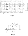
- Fig. 1 shows a schematic circuit diagram of a vehicle-sided circuit arrangement 1 of a system for inductive power transfer to the vehicle.
- the circuit arrangement 1 comprises a pick-up arrangement 2, static compensating elements C1, C2, C3 and variable compensating arrangements CV1, CV2, CV3.
- the circuit arrangement 1 comprises three phases. It is shown, that the pick-up arrangement 2 comprises the source elements S1, S2, S3, leakage inductances L1, L2, L3 and phase resistances R1, R2, R3. In each phase, the respective source element S1, S2, S3, the respective leakage inductance L1, L2, L3 and the respective phase resistance R1, R2, R3 are connected in series.
- the pick-up arrangement 2 generates alternating phase currents I1, I2, I3 during an inductive power transfer.
- the source elements S1, S2, S3 can be coils providing secondary windings for receiving a magnetic field generated by route-sided primary windings (not shown).
- Each phase further comprises one static compensating element C1, C2, C3 which is provided by capacitor with a predetermined capacitance respectively.
- These static compensating elements C1, C2, C3 are used to tune the circuit arrangement 1 such that the resonant frequencies provided by the series connections of the leakage inductances L1, L2, L3, the phase resistances R1, R2, R3 and the static compensating elements C1, C2, C3 each correspond to an operating frequency of the inductive power transfer which can e.g. be 20 kHz.
- Each phase further comprises one variable compensating arrangement CV1, CV2, CV3 which is shown in Fig. 2 in more detail. In each phase, the pick-up arrangement 2, i.e.
- the series connection of the respective source element S1, S2, S3, the respective leakage inductance L1, L2, L3 and the respective phase resistance R1, R2, R3, is connected in series to the respective static compensating element C1, C2, C3 and the respective variable compensating arrangement CV1, CV2, CV3.
- a load 3 which is connected to output terminals T1, T2, T3 of the circuit arrangement 1. Instead of a load 3, it is possible to connect a rectifier to the output terminals T1, T2, T3 to generate a direct current voltage which can be used for charging a traction battery or to provide electric energy to sub-systems of the electric vehicle.
- an overall or resulting impedance of the circuit arrangement 1 is given by the series connection of the respective leakage inductance L1, L2, L3, the respective phase resistance R1, R2, R3, the respective static compensating element C1, C2, C3 and the respective variable compensating arrangement CV1, CV2, CV3.
- an impedance, in particular a capacitance, of the variable compensating arrangements CV1, CV2, CV3 can be varied, the resulting or overall impedance of each phase of the circuit arrangement 1 can be varied, too. This, in turn, allows compensating a change of the impedances of the leakage inductance L1, L2, L3, the phase resistance R1, R2, R3 and/or the static compensating element C1, C2, C3.
- Fig. 2 shows a schematic diagram of a proposed variable compensating arrangement CV.
- the variable compensating arrangement CV comprises a capacitive element Cx, a first switching element S1 and a second switching element S2. Furthermore, the variable compensating arrangement CV comprises a first diode D1 and a second diode D2.
- the first diode D1 is connected anti-parallel to the first switching element S1.
- the second diode D2 is connected anti-parallel to the second switching element S2.
- the switching elements S1, S2 can be semiconductor switches.
- the series connection of the first and the second switching element S1, S2 is connected in parallel to the capacitive element Cx of the variable compensating arrangement CV. It is shown that a conducting direction of the first switching element S1, which is symbolized by an arrow 4, is opposite to a conducting direction of the second switching element S2, which is symbolized by arrow 5.
- phase current Ip which corresponds to one of the phase currents I1, I2, I3 shown in Fig. 1 .
- a current I Cx flowing through the capacitance Cx is shown.
- the shown variable compensating arrangement CV corresponds to one of the variable compensating arrangements CV1, CV2, CV3 shown in Fig. 1 .
- Fig. 3 an exemplary time course of switching signals SS1, SS2 of the first and the second switching element S1, S2 (see Fig. 2 ), a phase current Ip, a voltage U Cx falling across a capacitive element Cx of the variable compensating arrangement CV (see Fig. 2 ), a current I Cx flowing through the capacitive element Cx and a phase voltage Up are shown.
- the switching signals SS1, SS2 can be high level signals H or low level signals L. If a high level signal H is applied, the switching element S1, S2 is operated in a second operating mode (closed state) and if a low level signal L is applied, the switching element S1, S2 is operated in a first operating mode (opened state).
- the switching signals SS1, SS2 can be gate signals of semiconductor switches which provide the first and the second switching element S1, S2.
- a high level signal H is applied to the second switching element S2.
- a low level signal L is applied to the first switching element S1.
- the phase current Ip is negative.
- the phase current Ip flows through the second switching element S2 and the first diode D1.
- the voltage U Cx falling across the capacitive element Cx is zero.
- the switching signal SS2 of the second switching element S2 is turned to a low level signal L.
- an operating mode of the second switching element is changed from a second operating mode (closed state) to a first operating mode (opened state).
- the switch arrangement i.e. the series connection of the first and the second switching element S1, S2, blocks the phase current Ip which consequently charges the capacitive element Cx.
- an absolute value of the voltage U Cx increases.
- the first switching signal SS1 of the first switching element S1 is turned to a high level signal H.
- the second switching instant t2 corresponds to a zero crossing instant of the phase current Ip.
- the time axis in Fig. 3 shows a phase angle ⁇ t and the second switching instant t2 corresponds to a phase angle of - ⁇ /2 with reference to the phase angle of the phase voltage Up.
- a time difference between the first switching instant t1 and the second switching instant t2 is expressed in terms of a phase angle ⁇ .
- the angle ⁇ is chosen such that a predetermined maximum absolute value of the voltage U Cx during the charging of the capacitive element Cx is achieved.
- the capacitive element Cx is discharged and the absolute value of the voltage U Cx decreases, wherein the current I Cx resulting from the discharge provides the phase current Ip.
- the capacitive element Cx is completely discharged and the phase current Ip changes its current path and flows through the first switching element S1 and the second diode D2.
- the first switching signal SS1 is turned from a high level signal H to a low level signal L.
- the phase current consequently corresponds to the current I Cx charging the capacitive element Cx.
- the second switching signal SS2 of the second switching element S2 is turned from a low level signal L to a high level signal H.
- the capacitive element Cx discharges, wherein the current I Cx resulting from the discharge provides the phase current Ip.
- a time difference between the third and the fourth switching instant t4, t5 can be expressed by the angle ⁇ .
- the capacitive element Cx is completely discharged and the phase current Ip changes its current path and now flows through the second switching element S2 and the first diode D1.
- a control unit (not shown) can be used to synchronize the switching instances t1, t2, t4, t5 with the phase current Ip flowing through the circuit arrangement 1 (see Fig. 1 ).
- the control unit can e.g. generate gate pulses or gate signals which can be equal to the switching signals SS1, SS2 shown in Fig. 3 .
- the switching elements will be closed and the series connection of the switching elements S1, S2 acts as a bypass for the phase current Ip with respect to the capacitive element Cx.
- the switching elements S1, S2 will be opened and closed periodically with a certain leading edge phase-delay (which corresponds to the phase angle ⁇ ) to the zero crossing instants t2, t5 of the phase current Ip.
- the phase-delay time (denoted by ⁇ ) can be a control variable for controlling the resulting capacitance provided by the variable compensating arrangement CV (see Fig. 2 ).
- the switch openings e.g. at the first and the third switching time instant t1, t4, are triggered by a control logic.
- the switch closings e.g. at the second and the fourth switching instant t2, t5 occurs autonomously due to the diodes D1, D2 placed inside the bidirectional switch arrangement provided by the series connection of the first and the second switching element S1, S2.
Landscapes
- Engineering & Computer Science (AREA)
- Power Engineering (AREA)
- Transportation (AREA)
- Mechanical Engineering (AREA)
- Computer Networks & Wireless Communication (AREA)
- Physics & Mathematics (AREA)
- Electromagnetism (AREA)
- Life Sciences & Earth Sciences (AREA)
- Sustainable Development (AREA)
- Sustainable Energy (AREA)
- Inverter Devices (AREA)
- Charge And Discharge Circuits For Batteries Or The Like (AREA)
Claims (15)
- Schaltungsanordnung, insbesondere eine Schaltungsanordnung eines Elektrofahrzeugs für die induktive Übertragung von Energie zum Fahrzeug,
wobei die Schaltungsanordnung (1) eine Empfangsanordnung (2) und zumindest eine variable Kompensationsanordnung (CV, CV1, CV2 , CV3) umfasst, wobei die variable Kompensationsanordnung (CV, CV1, CV2 , CV3) ein kapazitives Element (Cx) umfasst,
dadurch gekennzeichnet, dass
die variable Kompensationsanordnung (CV, CV1, CV2 , CV3) außerdem ein erstes Schaltelement (S1) und ein zweites Schaltelement (S2) umfasst, wobei das erste Schaltelement (S1) und das zweite Schaltelement (S2) in Reihe geschaltet sind, wobei die Reihenschaltung des ersten und des zweiten Schaltelements (S1, S2) parallel zum kapazitiven Element (Cx) der variablen Kompensationsanordnung (CV, CV1, CV2 , CV3) geschaltet ist. - Schaltungsanordnung nach Anspruch 1, wobei die variable Kompensationsanordnung (CV, CV1, CV2, CV3) in Reihe mit der Empfangsanordnung (2) geschaltet ist.
- Schaltungsanordnung nach einem der Ansprüche 1 oder 2, wobei die Schaltungsanordnung (1) mindestens ein statisches Kompensationselement (C1, C2, C3) umfasst, wobei die Empfangsanordnung (2), das statische Kompensationselement (C1, C2, C3) und die variable Kompensationsanordnung (CV, CV1, CV2, CV3) in Reihe geschaltet sind.
- Schaltungsanordnung nach einem der Ansprüche 1 bis 3, wobei das erste Schaltelement (S1) und/oder das zweite Schaltelement (S2) (ein) Halbleiterelement(e) ist/sind.
- Schaltungsanordnung nach einem der Ansprüche 1 bis 4, wobei das erste Schaltelement (S1) eine Durchlassrichtung aufweist und das zweite Schaltelement (S2) eine Durchlassrichtung aufweist, wobei das erste und das zweite Schaltelement (S1, S2) so verbunden sind , dass die Durchlassrichtung des ersten Schaltelementes (S1) zur Durchlassrichtung des zweiten Schaltelements (S2) entgegengesetzt ist.
- Schaltungsanordnung nach einem der Ansprüche 1 bis 5, wobei eine erste Diode (D1) gegenparallel zum ersten Schaltelement (D1) geschaltet ist und eine zweite Diode (D2) gegenparallel zum zweiten Schaltelement (S2) geschaltet ist.
- Schaltungsanordnung nach einem der Ansprüche 1 bis 6, wobei die Schaltungsanordnung (1) mindestens ein Stromerfassungsmittel zum Erfassen eines Phasenstroms (I1, I2, I3, Ip) der Schaltungsanordnung (1) umfasst, wobei Schaltzeiten (t1, t2, t4 , t5) des ersten und des zweiten Schaltelements (S1, S2) in Abhängigkeit vom Phasenstrom (I1, I2, I3, Ip) steuerbar sind.
- Schaltungsanordnung nach einem der Ansprüche 1 bis 7, wobei die Schaltungsanordnung (1) mindestens ein Erfassungsmittel zum Erfassen einer Spannung (Ucx) über dem kapazitiven Element (Cx) der variablen Kompensationsanordnung (CV, CV1, CV2, CV3) umfasst, wobei die Schaltzeiten (t1, t2, t4 , t5) des ersten und des zweiten Schaltelements (S1, S2) in Abhängigkeit von der Spannung (Ucx) steuerbar sind.
- Schaltungsanordnung nach einem der Ansprüche 1 bis 8, wobei die Schaltungsanordnung (1) eine Steuereinheit umfasst, die angepasst ist, einen Betriebsmodus des ersten und des zweiten Schaltelements (S1, S2) zu steuern.
- Schaltungsanordnung nach einem der Ansprüche 1 bis 9, wobei die Schaltungsanordnung (1) drei Phasen umfasst, wobei jede der Phasen mindestens eine variable Kompensationsanordnung (CV1, CV2, CV3) umfasst.
- Verfahren zum Betrieb einer Schaltungsanordnung nach einem der Ansprüche 1 bis 10, wobei ein Betriebsmodus des ersten und des zweiten Schaltelements (S1, S2) derart gesteuert wird, dass die variable Kompensationsanordnung (CV, CV1, CV2 , CV3) eine gewünschte Impedanz bereitstellt.
- Verfahren nach Anspruch 11, wobei das erste und das zweite Schaltelement (S1, S2) in einem inaktiven Betriebsmodus der variablen Kompensationsanordnung (CV, CV1, CV2, CV3) geschlossen sind.
- Verfahren nach einem der Ansprüche 11 oder 12, wobei das erste Schaltelement (S1) und/oder das zweite Schaltelement (S2) in periodischer Weise synchronisiert mit dem Phasenstrom (I1, I2, I3, Ip) der Schaltungsanordnung (1) betrieben wird/werden.
- Verfahren nach einem der Ansprüche 11 bis 13, wobei die Schaltzeiten (t1, t2, t4 , t5) des ersten Schaltelements (S1) und des zweiten Schaltelements (S2) einem Zeitpunkt entsprechen, bei dem ein Phasenstrom (I1, I2, I3, Ip) kleiner als ein vorgegebener Wert wird oder eine Spannung (Um) über dem kapazitiven Element (Cx) der variablen Kompensationsanordnung (CV, CV1, CV2, CV3) kleiner als ein vorgegebener Wert wird.
- Verfahren nach Anspruch 14, wobei die Schaltzeiten (t1, t2, t4 , t5) des ersten Schaltelements (S1) und des zweiten Schaltelements (S2) einem Zeitpunkt entsprechen, bei dem ein Phasenstrom (I1, I2, I3, Ip) null wird oder die Spannung (Ucx) über dem kapazitiven Element (Cx) der variablen Kompensationsanordnung (CV, CV1, CV2, CV3) null wird.
Applications Claiming Priority (2)
| Application Number | Priority Date | Filing Date | Title |
|---|---|---|---|
| GB1219724.0A GB2507533A (en) | 2012-11-02 | 2012-11-02 | Inductive power receiver having compensating arrangement |
| PCT/EP2013/072686 WO2014067984A2 (en) | 2012-11-02 | 2013-10-30 | Circuit arrangement and method of operating a circuit arrangement |
Publications (3)
| Publication Number | Publication Date |
|---|---|
| EP2914455A2 EP2914455A2 (de) | 2015-09-09 |
| EP2914455B1 EP2914455B1 (de) | 2016-07-06 |
| EP2914455B9 true EP2914455B9 (de) | 2016-10-05 |
Family
ID=47359052
Family Applications (1)
| Application Number | Title | Priority Date | Filing Date |
|---|---|---|---|
| EP13783932.0A Active EP2914455B9 (de) | 2012-11-02 | 2013-10-30 | Schaltungsanordnung umfassend aufnehmeranordnung und variable kompensationsanordnung, und verfahren |
Country Status (7)
| Country | Link |
|---|---|
| US (1) | US9809124B2 (de) |
| EP (1) | EP2914455B9 (de) |
| CN (1) | CN104736380B (de) |
| CA (1) | CA2885885A1 (de) |
| ES (1) | ES2590553T3 (de) |
| GB (1) | GB2507533A (de) |
| WO (1) | WO2014067984A2 (de) |
Families Citing this family (9)
| Publication number | Priority date | Publication date | Assignee | Title |
|---|---|---|---|---|
| EP2462679B1 (de) * | 2009-08-07 | 2022-09-28 | Auckland UniServices Limited | Induktives stromübertragungssystem |
| GB2530730A (en) * | 2014-09-29 | 2016-04-06 | Bombardier Transp Gmbh | Method of and control system for operating a circuit arrangement |
| US10355530B2 (en) * | 2015-03-12 | 2019-07-16 | Panasonic Intellectual Property Management Co., Ltd. | Non-contact power supply apparatus, program, method for controlling non-contact power supply apparatus, and non-contact power transmission system |
| GB2537827A (en) * | 2015-04-23 | 2016-11-02 | Bombardier Transp Gmbh | A circuit arrangement and a method of operating a circuit arrangement for a system for inductive power transfer |
| WO2018023882A1 (zh) * | 2016-08-04 | 2018-02-08 | 中惠创智无线供电技术有限公司 | 一种限幅控制电路、装置及方法 |
| GB2560938A (en) | 2017-03-29 | 2018-10-03 | Bombardier Primove Gmbh | A voltage-controllable capacitive device, a method for manufacturing such a device and a method for operating such a device and a device of a system |
| GB2580122A (en) | 2018-12-21 | 2020-07-15 | Bombardier Primove Gmbh | Inductive power transfer with reduced electromagnetic interactions within a conductor arrangement |
| KR102805469B1 (ko) * | 2020-05-06 | 2025-05-09 | 현대자동차주식회사 | 차량용 obc 제어 장치, 그를 포함한 시스템 및 그 방법 |
| NO347044B1 (en) * | 2021-10-11 | 2023-04-24 | Kongsberg Maritime As | Onboard medium-voltage vessel electric charging apparatus and method for onboard charging. |
Family Cites Families (19)
| Publication number | Priority date | Publication date | Assignee | Title |
|---|---|---|---|---|
| US5207304A (en) | 1991-12-03 | 1993-05-04 | The Regents Of The University Of California | Inductive energization system and method for vehicles |
| EP0640254B1 (de) | 1992-05-10 | 2001-08-01 | Auckland Uniservices Limited | System zur berührungslosen energieübertragung |
| WO1994024622A1 (en) * | 1993-04-19 | 1994-10-27 | Electric Power Research Institute | Turnoff thyristor controlled series compensation system |
| KR20010032834A (ko) | 1997-12-05 | 2001-04-25 | 마크 버게스 | 1차 컨덕터에 전력을 공급하는 장치 |
| JP3450690B2 (ja) * | 1998-01-20 | 2003-09-29 | 三菱電機株式会社 | 電力系統の補償制御装置 |
| JP4614961B2 (ja) * | 2003-05-23 | 2011-01-19 | オークランド ユニサービシズ リミテッド | 誘導結合電力伝達システムを制御する方法および装置 |
| JP4453741B2 (ja) | 2007-10-25 | 2010-04-21 | トヨタ自動車株式会社 | 電動車両および車両用給電装置 |
| CN103259344B (zh) * | 2007-12-21 | 2016-08-10 | 捷通国际有限公司 | 用于感应功率传输的电路 |
| JP5417346B2 (ja) * | 2008-02-28 | 2014-02-12 | ペレグリン セミコンダクター コーポレーション | 集積回路素子内でキャパシタをデジタル処理で同調するときに用いられる方法及び装置 |
| US8497601B2 (en) * | 2008-09-27 | 2013-07-30 | Witricity Corporation | Wireless energy transfer converters |
| WO2010041321A1 (ja) * | 2008-10-09 | 2010-04-15 | トヨタ自動車株式会社 | 非接触電力伝達装置および非接触電力伝達装置を備える車両 |
| JP4457162B1 (ja) * | 2008-10-27 | 2010-04-28 | 株式会社MERSTech | 交流電圧制御装置 |
| WO2011046453A1 (en) | 2009-10-12 | 2011-04-21 | Auckland Uniservices Limited | Inductively controlled series resonant ac power transfer |
| CN102280944A (zh) | 2010-06-12 | 2011-12-14 | 上海鸿隆电子技术有限公司 | 磁共振式无线供电电路 |
| US8310202B2 (en) * | 2010-08-17 | 2012-11-13 | Ut-Battelle, Llc | Off-resonance frequency operation for power transfer in a loosely coupled air core transformer |
| NZ587780A (en) | 2010-09-03 | 2013-06-28 | Auckland Uniservices Ltd | Inductive power transfer pick-up circuit with additional resonant components that can reduce power supplied to a load |
| US20120313728A1 (en) * | 2011-06-10 | 2012-12-13 | Cairo Jr John Louis | Apparatus for Capturing Electric Distribution System Harmonics for Powering Loads |
| GB2491652A (en) * | 2011-06-10 | 2012-12-12 | Bombardier Transp Gmbh | System and Method for Transferring Electric Energy to a Vehicle Using a Plurality of Segments of a Conductor Arrangement |
| WO2013057896A1 (ja) * | 2011-10-18 | 2013-04-25 | 株式会社アドバンテスト | ワイヤレス受電装置、ワイヤレス給電装置およびワイヤレス給電システム |
-
2012
- 2012-11-02 GB GB1219724.0A patent/GB2507533A/en not_active Withdrawn
-
2013
- 2013-10-30 WO PCT/EP2013/072686 patent/WO2014067984A2/en not_active Ceased
- 2013-10-30 US US14/434,578 patent/US9809124B2/en active Active
- 2013-10-30 CA CA2885885A patent/CA2885885A1/en not_active Abandoned
- 2013-10-30 ES ES13783932.0T patent/ES2590553T3/es active Active
- 2013-10-30 CN CN201380054855.6A patent/CN104736380B/zh active Active
- 2013-10-30 EP EP13783932.0A patent/EP2914455B9/de active Active
Also Published As
| Publication number | Publication date |
|---|---|
| GB2507533A (en) | 2014-05-07 |
| CA2885885A1 (en) | 2014-05-08 |
| EP2914455B1 (de) | 2016-07-06 |
| US20150298562A1 (en) | 2015-10-22 |
| GB201219724D0 (en) | 2012-12-12 |
| CN104736380B (zh) | 2018-01-12 |
| ES2590553T3 (es) | 2016-11-22 |
| CN104736380A (zh) | 2015-06-24 |
| WO2014067984A2 (en) | 2014-05-08 |
| HK1214212A1 (en) | 2016-07-22 |
| WO2014067984A3 (en) | 2014-10-23 |
| EP2914455A2 (de) | 2015-09-09 |
| US9809124B2 (en) | 2017-11-07 |
Similar Documents
| Publication | Publication Date | Title |
|---|---|---|
| EP2914455B9 (de) | Schaltungsanordnung umfassend aufnehmeranordnung und variable kompensationsanordnung, und verfahren | |
| EP2895350B1 (de) | Schaltungsanordnung und verfahren zum betrieb einer schaltungsanordnung | |
| US7710751B2 (en) | Secondary-side power receiving circuit of noncontact power supplying equipment | |
| EP3177478B1 (de) | Verfahren und vorrichtung zur abstimmung und steuerung von doppelpaar-induktivenergieübertragungssystemen | |
| US10305393B2 (en) | Resonant power supply with self tuning | |
| WO2015006673A1 (en) | Double-sided lcc compensation method for wireless power transfer | |
| JP2009201211A (ja) | 電力供給システム | |
| US20060082324A1 (en) | Decoupling circuits | |
| EP3201033B1 (de) | Verfahren und steuerungssystem zum betrieb einer schaltungsanordnung | |
| HK1214212B (en) | Circuit arrangement comprising pick-up and variable compensating arrangement, and method | |
| US20240270093A1 (en) | Charging Station for Electric Vehicles | |
| EP3528365B1 (de) | Wende- und gleichrichtervorrichtung für drahtlosen stromübertragungsempfänger | |
| KR102160557B1 (ko) | 배터리 충전 장치 및 방법 | |
| US20150091515A1 (en) | Circuit for wireless energy-transfer by way of an alternating magnetic field, and electrically powered vehicle | |
| HK1209700B (en) | Circuit arrangement and method of operating a circuit arrangement |
Legal Events
| Date | Code | Title | Description |
|---|---|---|---|
| PUAI | Public reference made under article 153(3) epc to a published international application that has entered the european phase |
Free format text: ORIGINAL CODE: 0009012 |
|
| 17P | Request for examination filed |
Effective date: 20150427 |
|
| AK | Designated contracting states |
Kind code of ref document: A2 Designated state(s): AL AT BE BG CH CY CZ DE DK EE ES FI FR GB GR HR HU IE IS IT LI LT LU LV MC MK MT NL NO PL PT RO RS SE SI SK SM TR |
|
| AX | Request for extension of the european patent |
Extension state: BA ME |
|
| RIN1 | Information on inventor provided before grant (corrected) |
Inventor name: CZAINSKI, ROBERT Inventor name: ARNOLD, RINALDO |
|
| GRAP | Despatch of communication of intention to grant a patent |
Free format text: ORIGINAL CODE: EPIDOSNIGR1 |
|
| DAX | Request for extension of the european patent (deleted) | ||
| INTG | Intention to grant announced |
Effective date: 20160128 |
|
| RAP1 | Party data changed (applicant data changed or rights of an application transferred) |
Owner name: BOMBARDIER PRIMOVE GMBH |
|
| RIN1 | Information on inventor provided before grant (corrected) |
Inventor name: CZAINSKI, ROBERT Inventor name: ARNOLD, RINALDO |
|
| RAP1 | Party data changed (applicant data changed or rights of an application transferred) |
Owner name: BOMBARDIER PRIMOVE GMBH |
|
| GRAS | Grant fee paid |
Free format text: ORIGINAL CODE: EPIDOSNIGR3 |
|
| GRAA | (expected) grant |
Free format text: ORIGINAL CODE: 0009210 |
|
| AK | Designated contracting states |
Kind code of ref document: B1 Designated state(s): AL AT BE BG CH CY CZ DE DK EE ES FI FR GB GR HR HU IE IS IT LI LT LU LV MC MK MT NL NO PL PT RO RS SE SI SK SM TR |
|
| REG | Reference to a national code |
Ref country code: GB Ref legal event code: FG4D |
|
| REG | Reference to a national code |
Ref country code: AT Ref legal event code: REF Ref document number: 810443 Country of ref document: AT Kind code of ref document: T Effective date: 20160715 Ref country code: CH Ref legal event code: EP |
|
| REG | Reference to a national code |
Ref country code: HK Ref legal event code: DE Ref document number: 1214212 Country of ref document: HK |
|
| REG | Reference to a national code |
Ref country code: IE Ref legal event code: FG4D |
|
| REG | Reference to a national code |
Ref country code: DE Ref legal event code: R096 Ref document number: 602013009224 Country of ref document: DE |
|
| REG | Reference to a national code |
Ref country code: FR Ref legal event code: PLFP Year of fee payment: 4 |
|
| REG | Reference to a national code |
Ref country code: NL Ref legal event code: MP Effective date: 20160706 |
|
| REG | Reference to a national code |
Ref country code: LT Ref legal event code: MG4D |
|
| REG | Reference to a national code |
Ref country code: ES Ref legal event code: FG2A Ref document number: 2590553 Country of ref document: ES Kind code of ref document: T3 Effective date: 20161122 |
|
| REG | Reference to a national code |
Ref country code: AT Ref legal event code: MK05 Ref document number: 810443 Country of ref document: AT Kind code of ref document: T Effective date: 20160706 |
|
| PG25 | Lapsed in a contracting state [announced via postgrant information from national office to epo] |
Ref country code: IS Free format text: LAPSE BECAUSE OF FAILURE TO SUBMIT A TRANSLATION OF THE DESCRIPTION OR TO PAY THE FEE WITHIN THE PRESCRIBED TIME-LIMIT Effective date: 20161106 Ref country code: RS Free format text: LAPSE BECAUSE OF FAILURE TO SUBMIT A TRANSLATION OF THE DESCRIPTION OR TO PAY THE FEE WITHIN THE PRESCRIBED TIME-LIMIT Effective date: 20160706 Ref country code: FI Free format text: LAPSE BECAUSE OF FAILURE TO SUBMIT A TRANSLATION OF THE DESCRIPTION OR TO PAY THE FEE WITHIN THE PRESCRIBED TIME-LIMIT Effective date: 20160706 Ref country code: HR Free format text: LAPSE BECAUSE OF FAILURE TO SUBMIT A TRANSLATION OF THE DESCRIPTION OR TO PAY THE FEE WITHIN THE PRESCRIBED TIME-LIMIT Effective date: 20160706 Ref country code: NL Free format text: LAPSE BECAUSE OF FAILURE TO SUBMIT A TRANSLATION OF THE DESCRIPTION OR TO PAY THE FEE WITHIN THE PRESCRIBED TIME-LIMIT Effective date: 20160706 Ref country code: NO Free format text: LAPSE BECAUSE OF FAILURE TO SUBMIT A TRANSLATION OF THE DESCRIPTION OR TO PAY THE FEE WITHIN THE PRESCRIBED TIME-LIMIT Effective date: 20161006 Ref country code: LT Free format text: LAPSE BECAUSE OF FAILURE TO SUBMIT A TRANSLATION OF THE DESCRIPTION OR TO PAY THE FEE WITHIN THE PRESCRIBED TIME-LIMIT Effective date: 20160706 |
|
| PG25 | Lapsed in a contracting state [announced via postgrant information from national office to epo] |
Ref country code: GR Free format text: LAPSE BECAUSE OF FAILURE TO SUBMIT A TRANSLATION OF THE DESCRIPTION OR TO PAY THE FEE WITHIN THE PRESCRIBED TIME-LIMIT Effective date: 20161007 Ref country code: SE Free format text: LAPSE BECAUSE OF FAILURE TO SUBMIT A TRANSLATION OF THE DESCRIPTION OR TO PAY THE FEE WITHIN THE PRESCRIBED TIME-LIMIT Effective date: 20160706 Ref country code: PL Free format text: LAPSE BECAUSE OF FAILURE TO SUBMIT A TRANSLATION OF THE DESCRIPTION OR TO PAY THE FEE WITHIN THE PRESCRIBED TIME-LIMIT Effective date: 20160706 Ref country code: PT Free format text: LAPSE BECAUSE OF FAILURE TO SUBMIT A TRANSLATION OF THE DESCRIPTION OR TO PAY THE FEE WITHIN THE PRESCRIBED TIME-LIMIT Effective date: 20161107 Ref country code: BE Free format text: LAPSE BECAUSE OF NON-PAYMENT OF DUE FEES Effective date: 20160706 Ref country code: LV Free format text: LAPSE BECAUSE OF FAILURE TO SUBMIT A TRANSLATION OF THE DESCRIPTION OR TO PAY THE FEE WITHIN THE PRESCRIBED TIME-LIMIT Effective date: 20160706 Ref country code: AT Free format text: LAPSE BECAUSE OF FAILURE TO SUBMIT A TRANSLATION OF THE DESCRIPTION OR TO PAY THE FEE WITHIN THE PRESCRIBED TIME-LIMIT Effective date: 20160706 |
|
| REG | Reference to a national code |
Ref country code: DE Ref legal event code: R097 Ref document number: 602013009224 Country of ref document: DE |
|
| PG25 | Lapsed in a contracting state [announced via postgrant information from national office to epo] |
Ref country code: RO Free format text: LAPSE BECAUSE OF FAILURE TO SUBMIT A TRANSLATION OF THE DESCRIPTION OR TO PAY THE FEE WITHIN THE PRESCRIBED TIME-LIMIT Effective date: 20160706 Ref country code: EE Free format text: LAPSE BECAUSE OF FAILURE TO SUBMIT A TRANSLATION OF THE DESCRIPTION OR TO PAY THE FEE WITHIN THE PRESCRIBED TIME-LIMIT Effective date: 20160706 |
|
| PLBE | No opposition filed within time limit |
Free format text: ORIGINAL CODE: 0009261 |
|
| STAA | Information on the status of an ep patent application or granted ep patent |
Free format text: STATUS: NO OPPOSITION FILED WITHIN TIME LIMIT |
|
| PG25 | Lapsed in a contracting state [announced via postgrant information from national office to epo] |
Ref country code: BG Free format text: LAPSE BECAUSE OF FAILURE TO SUBMIT A TRANSLATION OF THE DESCRIPTION OR TO PAY THE FEE WITHIN THE PRESCRIBED TIME-LIMIT Effective date: 20161006 Ref country code: SM Free format text: LAPSE BECAUSE OF FAILURE TO SUBMIT A TRANSLATION OF THE DESCRIPTION OR TO PAY THE FEE WITHIN THE PRESCRIBED TIME-LIMIT Effective date: 20160706 Ref country code: DK Free format text: LAPSE BECAUSE OF FAILURE TO SUBMIT A TRANSLATION OF THE DESCRIPTION OR TO PAY THE FEE WITHIN THE PRESCRIBED TIME-LIMIT Effective date: 20160706 Ref country code: CZ Free format text: LAPSE BECAUSE OF FAILURE TO SUBMIT A TRANSLATION OF THE DESCRIPTION OR TO PAY THE FEE WITHIN THE PRESCRIBED TIME-LIMIT Effective date: 20160706 Ref country code: SK Free format text: LAPSE BECAUSE OF FAILURE TO SUBMIT A TRANSLATION OF THE DESCRIPTION OR TO PAY THE FEE WITHIN THE PRESCRIBED TIME-LIMIT Effective date: 20160706 |
|
| REG | Reference to a national code |
Ref country code: CH Ref legal event code: PL |
|
| 26N | No opposition filed |
Effective date: 20170407 |
|
| REG | Reference to a national code |
Ref country code: IE Ref legal event code: MM4A |
|
| PG25 | Lapsed in a contracting state [announced via postgrant information from national office to epo] |
Ref country code: CH Free format text: LAPSE BECAUSE OF NON-PAYMENT OF DUE FEES Effective date: 20161031 Ref country code: LI Free format text: LAPSE BECAUSE OF NON-PAYMENT OF DUE FEES Effective date: 20161031 |
|
| PG25 | Lapsed in a contracting state [announced via postgrant information from national office to epo] |
Ref country code: LU Free format text: LAPSE BECAUSE OF NON-PAYMENT OF DUE FEES Effective date: 20161030 Ref country code: SI Free format text: LAPSE BECAUSE OF FAILURE TO SUBMIT A TRANSLATION OF THE DESCRIPTION OR TO PAY THE FEE WITHIN THE PRESCRIBED TIME-LIMIT Effective date: 20160706 |
|
| REG | Reference to a national code |
Ref country code: HK Ref legal event code: GR Ref document number: 1214212 Country of ref document: HK |
|
| REG | Reference to a national code |
Ref country code: FR Ref legal event code: PLFP Year of fee payment: 5 |
|
| PG25 | Lapsed in a contracting state [announced via postgrant information from national office to epo] |
Ref country code: IE Free format text: LAPSE BECAUSE OF NON-PAYMENT OF DUE FEES Effective date: 20161030 |
|
| PGFP | Annual fee paid to national office [announced via postgrant information from national office to epo] |
Ref country code: ES Payment date: 20171121 Year of fee payment: 5 Ref country code: GB Payment date: 20171019 Year of fee payment: 5 |
|
| PG25 | Lapsed in a contracting state [announced via postgrant information from national office to epo] |
Ref country code: HU Free format text: LAPSE BECAUSE OF FAILURE TO SUBMIT A TRANSLATION OF THE DESCRIPTION OR TO PAY THE FEE WITHIN THE PRESCRIBED TIME-LIMIT; INVALID AB INITIO Effective date: 20131030 |
|
| PG25 | Lapsed in a contracting state [announced via postgrant information from national office to epo] |
Ref country code: CY Free format text: LAPSE BECAUSE OF FAILURE TO SUBMIT A TRANSLATION OF THE DESCRIPTION OR TO PAY THE FEE WITHIN THE PRESCRIBED TIME-LIMIT Effective date: 20160706 Ref country code: MK Free format text: LAPSE BECAUSE OF FAILURE TO SUBMIT A TRANSLATION OF THE DESCRIPTION OR TO PAY THE FEE WITHIN THE PRESCRIBED TIME-LIMIT Effective date: 20160706 Ref country code: MC Free format text: LAPSE BECAUSE OF FAILURE TO SUBMIT A TRANSLATION OF THE DESCRIPTION OR TO PAY THE FEE WITHIN THE PRESCRIBED TIME-LIMIT Effective date: 20160706 Ref country code: MT Free format text: LAPSE BECAUSE OF NON-PAYMENT OF DUE FEES Effective date: 20161031 |
|
| REG | Reference to a national code |
Ref country code: FR Ref legal event code: PLFP Year of fee payment: 6 |
|
| PG25 | Lapsed in a contracting state [announced via postgrant information from national office to epo] |
Ref country code: AL Free format text: LAPSE BECAUSE OF FAILURE TO SUBMIT A TRANSLATION OF THE DESCRIPTION OR TO PAY THE FEE WITHIN THE PRESCRIBED TIME-LIMIT Effective date: 20160706 Ref country code: TR Free format text: LAPSE BECAUSE OF FAILURE TO SUBMIT A TRANSLATION OF THE DESCRIPTION OR TO PAY THE FEE WITHIN THE PRESCRIBED TIME-LIMIT Effective date: 20160706 |
|
| REG | Reference to a national code |
Ref country code: DE Ref legal event code: R079 Ref document number: 602013009224 Country of ref document: DE Free format text: PREVIOUS MAIN CLASS: B60L0011180000 Ipc: B60L0050500000 |
|
| GBPC | Gb: european patent ceased through non-payment of renewal fee |
Effective date: 20181030 |
|
| PG25 | Lapsed in a contracting state [announced via postgrant information from national office to epo] |
Ref country code: GB Free format text: LAPSE BECAUSE OF NON-PAYMENT OF DUE FEES Effective date: 20181030 |
|
| REG | Reference to a national code |
Ref country code: ES Ref legal event code: FD2A Effective date: 20191203 |
|
| PG25 | Lapsed in a contracting state [announced via postgrant information from national office to epo] |
Ref country code: ES Free format text: LAPSE BECAUSE OF NON-PAYMENT OF DUE FEES Effective date: 20181031 |
|
| REG | Reference to a national code |
Ref country code: DE Ref legal event code: R081 Ref document number: 602013009224 Country of ref document: DE Owner name: ENRX IPT GMBH, DE Free format text: FORMER OWNER: BOMBARDIER PRIMOVE GMBH, 10785 BERLIN, DE |
|
| PGFP | Annual fee paid to national office [announced via postgrant information from national office to epo] |
Ref country code: DE Payment date: 20251021 Year of fee payment: 13 |
|
| PGFP | Annual fee paid to national office [announced via postgrant information from national office to epo] |
Ref country code: IT Payment date: 20251024 Year of fee payment: 13 |
|
| PGFP | Annual fee paid to national office [announced via postgrant information from national office to epo] |
Ref country code: FR Payment date: 20251030 Year of fee payment: 13 |