EP2911478A2 - Lightening apparatus having matrix-arranged light-emitting elements - Google Patents
Lightening apparatus having matrix-arranged light-emitting elements Download PDFInfo
- Publication number
- EP2911478A2 EP2911478A2 EP15155292.4A EP15155292A EP2911478A2 EP 2911478 A2 EP2911478 A2 EP 2911478A2 EP 15155292 A EP15155292 A EP 15155292A EP 2911478 A2 EP2911478 A2 EP 2911478A2
- Authority
- EP
- European Patent Office
- Prior art keywords
- reference voltage
- drive
- luminous
- voltage
- led elements
- Prior art date
- Legal status (The legal status is an assumption and is not a legal conclusion. Google has not performed a legal analysis and makes no representation as to the accuracy of the status listed.)
- Granted
Links
Images


Classifications
-
- B—PERFORMING OPERATIONS; TRANSPORTING
- B60—VEHICLES IN GENERAL
- B60Q—ARRANGEMENT OF SIGNALLING OR LIGHTING DEVICES, THE MOUNTING OR SUPPORTING THEREOF OR CIRCUITS THEREFOR, FOR VEHICLES IN GENERAL
- B60Q1/00—Arrangement of optical signalling or lighting devices, the mounting or supporting thereof or circuits therefor
- B60Q1/02—Arrangement of optical signalling or lighting devices, the mounting or supporting thereof or circuits therefor the devices being primarily intended to illuminate the way ahead or to illuminate other areas of way or environments
- B60Q1/04—Arrangement of optical signalling or lighting devices, the mounting or supporting thereof or circuits therefor the devices being primarily intended to illuminate the way ahead or to illuminate other areas of way or environments the devices being headlights
- B60Q1/14—Arrangement of optical signalling or lighting devices, the mounting or supporting thereof or circuits therefor the devices being primarily intended to illuminate the way ahead or to illuminate other areas of way or environments the devices being headlights having dimming means
- B60Q1/1415—Dimming circuits
- B60Q1/1423—Automatic dimming circuits, i.e. switching between high beam and low beam due to change of ambient light or light level in road traffic
- B60Q1/143—Automatic dimming circuits, i.e. switching between high beam and low beam due to change of ambient light or light level in road traffic combined with another condition, e.g. using vehicle recognition from camera images or activation of wipers
-
- B—PERFORMING OPERATIONS; TRANSPORTING
- B60—VEHICLES IN GENERAL
- B60Q—ARRANGEMENT OF SIGNALLING OR LIGHTING DEVICES, THE MOUNTING OR SUPPORTING THEREOF OR CIRCUITS THEREFOR, FOR VEHICLES IN GENERAL
- B60Q1/00—Arrangement of optical signalling or lighting devices, the mounting or supporting thereof or circuits therefor
- B60Q1/02—Arrangement of optical signalling or lighting devices, the mounting or supporting thereof or circuits therefor the devices being primarily intended to illuminate the way ahead or to illuminate other areas of way or environments
- B60Q1/04—Arrangement of optical signalling or lighting devices, the mounting or supporting thereof or circuits therefor the devices being primarily intended to illuminate the way ahead or to illuminate other areas of way or environments the devices being headlights
- B60Q1/06—Arrangement of optical signalling or lighting devices, the mounting or supporting thereof or circuits therefor the devices being primarily intended to illuminate the way ahead or to illuminate other areas of way or environments the devices being headlights adjustable, e.g. remotely-controlled from inside vehicle
- B60Q1/08—Arrangement of optical signalling or lighting devices, the mounting or supporting thereof or circuits therefor the devices being primarily intended to illuminate the way ahead or to illuminate other areas of way or environments the devices being headlights adjustable, e.g. remotely-controlled from inside vehicle automatically
- B60Q1/12—Arrangement of optical signalling or lighting devices, the mounting or supporting thereof or circuits therefor the devices being primarily intended to illuminate the way ahead or to illuminate other areas of way or environments the devices being headlights adjustable, e.g. remotely-controlled from inside vehicle automatically due to steering position
-
- B—PERFORMING OPERATIONS; TRANSPORTING
- B60—VEHICLES IN GENERAL
- B60Q—ARRANGEMENT OF SIGNALLING OR LIGHTING DEVICES, THE MOUNTING OR SUPPORTING THEREOF OR CIRCUITS THEREFOR, FOR VEHICLES IN GENERAL
- B60Q1/00—Arrangement of optical signalling or lighting devices, the mounting or supporting thereof or circuits therefor
- B60Q1/02—Arrangement of optical signalling or lighting devices, the mounting or supporting thereof or circuits therefor the devices being primarily intended to illuminate the way ahead or to illuminate other areas of way or environments
- B60Q1/04—Arrangement of optical signalling or lighting devices, the mounting or supporting thereof or circuits therefor the devices being primarily intended to illuminate the way ahead or to illuminate other areas of way or environments the devices being headlights
- B60Q1/14—Arrangement of optical signalling or lighting devices, the mounting or supporting thereof or circuits therefor the devices being primarily intended to illuminate the way ahead or to illuminate other areas of way or environments the devices being headlights having dimming means
- B60Q1/1415—Dimming circuits
- B60Q1/1423—Automatic dimming circuits, i.e. switching between high beam and low beam due to change of ambient light or light level in road traffic
-
- H—ELECTRICITY
- H05—ELECTRIC TECHNIQUES NOT OTHERWISE PROVIDED FOR
- H05B—ELECTRIC HEATING; ELECTRIC LIGHT SOURCES NOT OTHERWISE PROVIDED FOR; CIRCUIT ARRANGEMENTS FOR ELECTRIC LIGHT SOURCES, IN GENERAL
- H05B45/00—Circuit arrangements for operating light-emitting diodes [LED]
- H05B45/10—Controlling the intensity of the light
-
- H—ELECTRICITY
- H05—ELECTRIC TECHNIQUES NOT OTHERWISE PROVIDED FOR
- H05B—ELECTRIC HEATING; ELECTRIC LIGHT SOURCES NOT OTHERWISE PROVIDED FOR; CIRCUIT ARRANGEMENTS FOR ELECTRIC LIGHT SOURCES, IN GENERAL
- H05B45/00—Circuit arrangements for operating light-emitting diodes [LED]
- H05B45/40—Details of LED load circuits
- H05B45/44—Details of LED load circuits with an active control inside an LED matrix
- H05B45/46—Details of LED load circuits with an active control inside an LED matrix having LEDs disposed in parallel lines
-
- H—ELECTRICITY
- H05—ELECTRIC TECHNIQUES NOT OTHERWISE PROVIDED FOR
- H05B—ELECTRIC HEATING; ELECTRIC LIGHT SOURCES NOT OTHERWISE PROVIDED FOR; CIRCUIT ARRANGEMENTS FOR ELECTRIC LIGHT SOURCES, IN GENERAL
- H05B45/00—Circuit arrangements for operating light-emitting diodes [LED]
- H05B45/40—Details of LED load circuits
- H05B45/44—Details of LED load circuits with an active control inside an LED matrix
- H05B45/48—Details of LED load circuits with an active control inside an LED matrix having LEDs organised in strings and incorporating parallel shunting devices
-
- B—PERFORMING OPERATIONS; TRANSPORTING
- B60—VEHICLES IN GENERAL
- B60Q—ARRANGEMENT OF SIGNALLING OR LIGHTING DEVICES, THE MOUNTING OR SUPPORTING THEREOF OR CIRCUITS THEREFOR, FOR VEHICLES IN GENERAL
- B60Q2300/00—Indexing codes for automatically adjustable headlamps or automatically dimmable headlamps
- B60Q2300/05—Special features for controlling or switching of the light beam
- B60Q2300/054—Variable non-standard intensity, i.e. emission of various beam intensities different from standard intensities, e.g. continuous or stepped transitions of intensity
-
- B—PERFORMING OPERATIONS; TRANSPORTING
- B60—VEHICLES IN GENERAL
- B60Q—ARRANGEMENT OF SIGNALLING OR LIGHTING DEVICES, THE MOUNTING OR SUPPORTING THEREOF OR CIRCUITS THEREFOR, FOR VEHICLES IN GENERAL
- B60Q2300/00—Indexing codes for automatically adjustable headlamps or automatically dimmable headlamps
- B60Q2300/05—Special features for controlling or switching of the light beam
- B60Q2300/056—Special anti-blinding beams, e.g. a standard beam is chopped or moved in order not to blind
-
- B—PERFORMING OPERATIONS; TRANSPORTING
- B60—VEHICLES IN GENERAL
- B60Q—ARRANGEMENT OF SIGNALLING OR LIGHTING DEVICES, THE MOUNTING OR SUPPORTING THEREOF OR CIRCUITS THEREFOR, FOR VEHICLES IN GENERAL
- B60Q2300/00—Indexing codes for automatically adjustable headlamps or automatically dimmable headlamps
- B60Q2300/10—Indexing codes relating to particular vehicle conditions
- B60Q2300/12—Steering parameters
- B60Q2300/122—Steering angle
-
- B—PERFORMING OPERATIONS; TRANSPORTING
- B60—VEHICLES IN GENERAL
- B60Q—ARRANGEMENT OF SIGNALLING OR LIGHTING DEVICES, THE MOUNTING OR SUPPORTING THEREOF OR CIRCUITS THEREFOR, FOR VEHICLES IN GENERAL
- B60Q2300/00—Indexing codes for automatically adjustable headlamps or automatically dimmable headlamps
- B60Q2300/40—Indexing codes relating to other road users or special conditions
- B60Q2300/41—Indexing codes relating to other road users or special conditions preceding vehicle
-
- F—MECHANICAL ENGINEERING; LIGHTING; HEATING; WEAPONS; BLASTING
- F21—LIGHTING
- F21S—NON-PORTABLE LIGHTING DEVICES; SYSTEMS THEREOF; VEHICLE LIGHTING DEVICES SPECIALLY ADAPTED FOR VEHICLE EXTERIORS
- F21S41/00—Illuminating devices specially adapted for vehicle exteriors, e.g. headlamps
- F21S41/10—Illuminating devices specially adapted for vehicle exteriors, e.g. headlamps characterised by the light source
- F21S41/14—Illuminating devices specially adapted for vehicle exteriors, e.g. headlamps characterised by the light source characterised by the type of light source
- F21S41/141—Light emitting diodes [LED]
- F21S41/151—Light emitting diodes [LED] arranged in one or more lines
- F21S41/153—Light emitting diodes [LED] arranged in one or more lines arranged in a matrix
-
- F—MECHANICAL ENGINEERING; LIGHTING; HEATING; WEAPONS; BLASTING
- F21—LIGHTING
- F21S—NON-PORTABLE LIGHTING DEVICES; SYSTEMS THEREOF; VEHICLE LIGHTING DEVICES SPECIALLY ADAPTED FOR VEHICLE EXTERIORS
- F21S41/00—Illuminating devices specially adapted for vehicle exteriors, e.g. headlamps
- F21S41/60—Illuminating devices specially adapted for vehicle exteriors, e.g. headlamps characterised by a variable light distribution
- F21S41/65—Illuminating devices specially adapted for vehicle exteriors, e.g. headlamps characterised by a variable light distribution by acting on light sources
- F21S41/663—Illuminating devices specially adapted for vehicle exteriors, e.g. headlamps characterised by a variable light distribution by acting on light sources by switching light sources
Definitions
- the presently disclosed subject matter relates to a lightening apparatus having a plurality of light-emitting elements such as light-emitting diode (LED) elements and organic or inorganic electro-luminescense (EL) elements arranged in a matrix.
- LED light-emitting diode
- EL electro-luminescense
- a lightening apparatus formed by LED elements arranged in a matrix including "m” rows and “n” columns has been used as a vehicle headlamp.
- luminous intensities of the LED elements are individually controlled to realize an adaptive drive beam (ADB) and an adaptive front-lighting system (AFS) (see: JP2013-54849A ).
- all cathode electrodes of the LED elements are commonly grounded, while there are a plurality of luminous drive voltage lines each connected to one of the LED elements.
- the luminous intensities of the LED elements can individually be controlled.
- the on-duty ratios d on /(d on +d off ) of the luminous drive voltages of Fig. 10A are shifted on the right side, to substantially change the optical direction of the LED panel 1 toward the right side.
- the duty ratio T1/(T1+T3) for one time-divisional driving is different from the duty ratio T3/(T3+T5) for another time-divisional driving, areas having different luminous intensities are created in the LED panel 1.
- the maximum luminous intensities of the first row, the second row, the third row, the fourth row and the fifth row are 20, 50, 80, 100 and 50, respectively, optimum light distribution patterns for vehicle headlamps whose luminous intensities are gradually changed as illustrated in Fig. 9B , 10B , 11B and 12B can be realized.
- the LED elements P 2, 1 , P 2, 2 , ⁇ , P 2, 20 for the second row and the LED elements P 6, 1 , P 6, 2 , ⁇ , P 6, 20 for the sixth row are time-divisionally driven by a dynamic driving method.
- the reference voltage driver 21 is a simple switching circuit, similar to the reference voltage driver 4 of Fig. 4C , which activates or switches the reference voltage line S5 over the entire luminous period T0.
- the LED elements P 4, 1 , P 4, 2 , ⁇ , P 4, 20 for the fourth row are driven by a static driving method.
- the luminous intensities of the LED elements P 5, 1 , P 5, 2 , ⁇ , P 5, 20 are ranged from 0 (dark) to 70 in accordance with the on-duty ratios of the luminous drive voltages E1, E2, ⁇ , E20.
- Fig. 15 which is a block circuit diagram of the reference voltage driver 2' of Fig. 14A
- the reference voltage driver 2' is constructed by a PWM circuit which includes latch circuits 21' 22' and 23' , down counters 24' , 25' and 26' , RS-type flip-flops 27' , 28' and 29' , and output amplifiers 30', 31' and 32' for generating voltages at the reference voltage lines S1, S2 and S5.
- the RS-type flip-flop 28' When the down counter 26' underflows to generate an underflow signal from its underflow terminal U, the RS-type flip-flop 28' is set, so that the voltage at the reference voltage line S2 rises. Simultaneously, the duty ratio value of the latch circuit 23' is loaded by the underflow signal of the down counter 25' in the down counter 26' . Then, the clock terminal C of the down counter 26' receives the clock signal CLK1 supplied from the light distribution control unit 8, so that the content of the down counter 26' is decremented by 1 in response to each pulse of the clock signal CLK1.
- the multiplexity of one reference voltage driver is 3.
- the multiplexity per one reference voltage driver can easily be increased to the number of rows of LED elements in the LED panel 1.
- Fig. 16A is a block circuit diagram illustrating a fourth embodiment of the lightening apparatus according to the presently disclosed subject matter
- Fig. 16B is a diagram for explaining the maximum luminous intensities of the LED elements of Fig. 16A .
- the LED elements P 1, 1 , P 1, 2 , ⁇ , P 1, 20 for the first row and the LED elements P 4, 1 , P 4, 2 , ⁇ , P 4, 20 for the fourth row are time-divisionally driven by a dynamic driving method.
- the LED elements P 2, 1 , P 2, 2 , ⁇ , P 2, 20 for the second row and the LED elements P 5, 1 , P 5, 2 , ⁇ , P 5, 20 for the fifth row are time-divisionally driven by a dynamic driving method.
- the LED elements P 3, 1 , P 3, 2 , ⁇ , P 3, 20 for the third row and the LED elements P 6, 1 , P 6, 2 , ⁇ , P 6, 20 for the sixth row are time-divisionally driven by a dynamic driving method.
- the luminous intensities of the LED elements P 2, 1 , P 2,2 , ⁇ , P 2, 20 are ranged from 0 (dark) to 40 in accordance with the on-duty ratios of the luminous drive voltages B1, B2, ⁇ , B20.
- the luminous intensities of the LED elements P 5, 1 , P 5, 2 , ⁇ , P 5, 20 are ranged from 0 (dark) to 60 in accordance with the on-duty ratios of the luminous drive voltages E1, E2, ⁇ , E20.
- all the reference voltage drivers can be constructed by multiplexing switching circuits. As a result, the number of voltage lines can be decreased as compared with that of Figs. 13A and 13B .
- Fig. 17A is a block circuit diagram illustrating a fifth embodiment of the lightening apparatus according to the presently disclosed subject matter
- Fig. 17B is a diagram for explaining the maximum luminous intensities of the LED elements of Fig. 17A .
- the center-side LED portion 1C is obtained by reducing the LED panel 1 of Fig. 7A . That is, the center-side LED portion 1C can be operated by reference voltage drivers 2C, 3C and 4C similar to the reference voltage drivers 2, 3 and 4, respectively, of Fig. 7A , and drive voltage drivers 5C, 6C and 7C similar to the drive voltage drivers 5, 6 and 7, respectively, of Fig. 7A . Therefore, the description on the operation of the center-side LED portion 1C is omitted.
- the left-side LED portion 1L is explained next in detail.
- the cathode electrodes of the LED elements P 1, 1 , P 1, 2 , P 1, 3 , P 1, 4 ; P 2 , 1 , P 2, 2 , P 2, 3 , P 2, 4 ; ⁇ ; and P 5, 1 , P 5, 2 , P 5, 3 , P 5, 4 are connected to reference voltage lines S1L, S2L, S3L, S4L and S5L, respectively.
- the anode electrodes of the LED elements P 1, 1 , P 2, 1 , P 3, 1 , P 4, 1 , P 5, 1 ; P 1, 2 , P 2, 2 , P 3, 2 , P 4, 2 ; P 1, 3 , P 2, 3 , P 3, 3 , P 4, 3 ; P 1, 4 , P 2,4 , P 3, 4 , P 4, 4 are connected to drive voltage lines L1, L2, L3, L4, respectively.
- a reference voltage driver 2L supplies reference voltages such as the ground voltage GND to the reference voltage lines S1L, S2L, S3L, S4L and S5L, while a drive voltage driver 5L supplies luminous drive voltages to the drive voltage lines L1, L2, L3 and L4.
- the right-side LED portion 1R is explained next in detail.
- each of the LED elements S 1, 1 , S 1, 2 , S 1, 15 , S 1, 16 ; S 1, 1 , S 2, 2 , S 2, 15 , S 2, 16 ; S 3, 1 , S 3, 2 , S 3, 15 , S 3, 16 has a longitudinal size twice those of the above-mentioned LED elements P 2, 4 , P 2, 5 , ⁇ and a traverse size twice those of the above-mentioned LED elements P 2, 4 , P 2, 5 , ⁇ , P 2, 13 and the like. Therefore, the area of each of the LED elements S 1, 1 , S 1, 2 , ⁇ is four times that of each of the LED elements P 2, 4 , P 2, 5 , ⁇ ,
- the cathode electrodes of the LED elements S 3, 1 and S 3, 2 are connected to a reference voltage line S3L, and the cathode electrodes of the LED elements S 4, 1 and S 4, 2 are connected to a reference voltage line S4L.
- the reference voltage lines S3L and S4L are time-divisionally activated by a reference voltage driver 3L with a luminous period ratio of 60:40.
- the anode electrodes of the LED elements S 3, 1 , S 4, 1 and S 3, 2 , S 4, 2 are connected to drive voltage lines L3 and L4, respectively, which are driven by a drive voltage driver 6L.
- the LED elements S 3, 1 and S 3, 2 for the third row and the LED elements S 4, 1 and S 4, 2 for the fourth row are time-divisionally driven by a dynamic driving method.
- the cathode electrodes of the LED elements S 1, 15 and S 1, 16 are connected to a reference voltage line S1R, and the cathode electrodes of the LED elements S 2, 15 and S 2, 16 are connected to a reference voltage line S2R.
- the reference voltage lines S1R and S2R are time-divisionally activated by a reference voltage driver 2R with a luminous period ratio of 50:50.
- the anode electrodes of the LED elements S 1, 15 , S 2, 15 and S 1, 16 , S 2, 16 are connected to drive voltage lines R1 and R2, respectively, which are driven by a drive voltage driver 5R.
- the LED elements S 1, 15 and S 1, 16 for the first row and the LED elements S 2, 15 and S 2, 16 for the second row are time-divisionally driven by a dynamic driving method.
- the cathode electrodes of the LED elements S 3, 15 and S 3, 16 are connected to a reference voltage line S3R, and the cathode electrodes of the LED elements S 4, 15 and S 4, 16 are connected to a reference voltage line S4R.
- the reference voltage lines S3R and S4R are time-divisionally activated by a reference voltage driver 3R with a luminous period ratio of 60:40.
- the anode electrodes of the LED elements S 3, 15 , S 4, 15 and S 3, 16 , S 4, 16 are connected to drive voltage lines R3 and R4, respectively, which are driven by a drive voltage driver 6R.
- the LED elements S 3, 15 and S 3, 16 for the third row and the LED elements S 4, 15 and S 4, 16 for the fourth row are time-divisionally driven by a dynamic driving method.
- the maximum luminous intensities of the LED elements S 3, 1 , S 3, 2 , Q 3, 3 , Q 3, 14 , S 3, 15 and S 3, 16 for the third row are 60, 60, 30, 30, 60 and 60, respectively.
- the maximum luminous intensities of the LED elements R 4, 1 , R 4, 2 , P 4, 3 , P 4, 14 , R 4, 15 and R 4, 16 for the fourth row are 40, 40, 10, 10, 40 and 40, respectively.
- the LED elements can have different sizes.
- the reference voltage drivers are connected to the cathode electrodes of the LED elements and the drive voltage drivers are connected to the anode electrodes of the LED elements; however, the reference voltage drivers can be connected to the anode electrodes of the LED elements and the drive voltage drivers can be connected to the cathode electrodes of the LED elements.
- the reference voltage drivers activate the reference voltage lines by supplying positive voltages such as the power supply voltage V CC thereto, while the on-duty ratio voltage of the drive voltage drivers is the low voltage such as the ground voltage.
Abstract
Description
- This application claims the priority benefit under 35 U.S.C. §119 to Japanese Patent Application No.
JP2014-031646 filed on February 21, 2014 - The presently disclosed subject matter relates to a lightening apparatus having a plurality of light-emitting elements such as light-emitting diode (LED) elements and organic or inorganic electro-luminescense (EL) elements arranged in a matrix.
- Conventionally, a lightening apparatus formed by LED elements arranged in a matrix including "m" rows and "n" columns has been used as a vehicle headlamp. In such a lightening apparatus, luminous intensities of the LED elements are individually controlled to realize an adaptive drive beam (ADB) and an adaptive front-lighting system (AFS) (see:
JP2013-54849A - For driving the conventional lightening apparatus, there are two driving methods: a static driving method and a dynamic driving method.
- In the static driving method, all cathode electrodes of the LED elements are commonly grounded, while there are a plurality of luminous drive voltage lines each connected to one of the LED elements. Thus, the luminous intensities of the LED elements can individually be controlled.
- In the static driving method, however, a large number of voltage lines, i. e. , "m×n" voltage lines are required, which would increase the lightening apparatus in size.
- On the other hand, in the dynamic driving method, there are "m" reference voltage lines each connected to all the cathode electrodes of the LED elements belonging to one row, and "n" drive voltage lines each connected to the LED elements belonging to one column. That is, only a small number of voltage lines, i.e., only (m+n) voltage lines are required, which would decrease the lightening apparatus in size as compared with those of the static driving method.
- In the dynamic driving method, however, since the rows of the LED elements are time-divisionally driven, when the number of rows of the LED elements is increased, the luminous period of the LED elements is decreased, which would decrease the luminous intensity.
- The presently disclosed subject matter seeks to solve one or more of the above-described problems.
- According to the presently disclosed subject matter, a lightening apparatus includes a plurality of light-emitting elements arranged in a matrix having "m" rows, "n" columns where "m" is an integer larger than 2 and "n" is a positive integer, at least two first reference voltage lines, and "m" first drive voltage lines. One of the light-emitting elements is located at each intersection between the first reference voltage lines and the first drive voltage lines. A first reference voltage driver is connected to the first reference voltage lines and adapted to time-divisionally switch the first reference voltage lines. A first drive voltage driver is connected to the first drive voltage lines and adapted to supply first luminous drive voltages to the first drive voltage lines in synchronization with time-divisional switching of the first reference voltage lines. At least one second reference voltage line and "m" second drive voltage lines are provided. One of the light-emitting elements is located at each intersection between the second reference voltage line and the second drive voltage lines. A second reference voltage driver is connected to the second reference voltage line and adapted to switch the second reference voltage line. A second drive voltage driver is connected to the second drive voltage lines and adapted to supply second luminous drive voltages to the second drive voltage lines in synchronization with switching of the second reference voltage line.
- The first reference voltage driver is operated by a dynamic driving method, and the second reference voltage driver is operated by either a dynamic driving method or a static driving method.
- According to the presently disclosed subject matter, even when the number of rows of the light-emitting elements is increased, the luminous intensity would not be decreased.
- The above and other advantages and features of the presently disclosed subject matter will be more apparent from the following description of certain embodiments, taken in conjunction with the accompanying drawings, wherein:
-
Fig. 1 is a block circuit diagram illustrating a first embodiment of the lightening apparatus according to the presently disclosed subject matter; -
Fig. 2 is a circuit diagram of the LED panel ofFig. 1 ; -
Fig. 3 is a timing diagram for explaining the operation of the lightening apparatus ofFig. 1 ; -
Figs. 4A, 4B and 4C are block circuit diagrams of the reference voltage drivers ofFig. 1 ; -
Figs. 5A, 5B and 5C are block circuit diagrams of the drive voltage drivers ofFig. 1 ; -
Fig. 6 is a block circuit diagram of the PWM circuit ofFig. 5A, 5B and 5C ; -
Fig. 7A is a simplified block circuit diagram of the lightening apparatus ofFig. 1 ; -
Fig. 7B is a diagram showing the maximum luminous intensities of the LED elements ofFig. 7A when the on-duty ratios of the luminous drive voltages are 100%; -
Fig. 8 is a flowchart for explaining the operation of the light distribution control unit ofFig. 1 ; -
Fig. 9A is a diagram showing a first example of the on-duty ratios of the luminous drive voltages ofFig. 1 ; -
Fig. 9B is a diagram showing the luminous intensities of the LED elements obtained by the luminous drive voltages ofFig. 9A ; -
Fig. 10A is a diagram showing a second example of the on-duty ratios of the luminous drive voltages ofFig. 1 ; -
Fig. 10B is a diagram showing the luminous intensities of the LED elements obtained by the luminous drive voltages ofFig. 10A ; -
Fig. 11A is a diagram showing a third example of the on-duty ratios of the luminous drive voltages ofFig. 1 ; -
Fig. 11B is a diagram showing the luminous intensities of the LED elements obtained by the luminous drive voltages ofFig. 11A ; -
Fig. 12A is a diagram showing a fourth example of the on-duty ratios of the luminous drive voltages ofFig. 1 ; -
Fig. 12B is a diagram showing the luminous intensities of the LED elements obtained by the luminous drive voltages ofFig. 12A ; -
Fig. 13A is a block circuit diagram illustrating a second embodiment of the lightening apparatus according to the presently disclosed subject matter; -
Fig. 13B is a diagram for explaining the maximum luminous intensities of the LED elements ofFig. 13A ; -
Fig. 14A is a block circuit diagram illustrating a third embodiment of the lightening apparatus according to the presently disclosed subject matter; -
Fig. 14B is a diagram for explaining the maximum luminous intensities of the LED elements ofFig. 14A ; -
Fig. 15 is a block circuit diagram of the reference voltage driver ofFig. 14A ; -
Fig. 16A is a block circuit diagram illustrating a fourth embodiment of the lightening apparatus according to the presently disclosed subject matter; -
Fig. 16B is a diagram for explaining the maximum luminous intensities of the LED elements ofFig. 16A ; -
Fig. 17A is a block circuit diagram illustrating a fifth embodiment of the lightening apparatus according to the presently disclosed subject matter; -
Fig. 17B is a diagram for explaining the maximum luminous intensities of the LED elements ofFig. 17A ; -
Fig. 18A is a block circuit diagram illustrating a sixth embodiment of the lightening apparatus according to the presently disclosed subject matter; and -
Fig. 18B is a diagram for explaining the maximum luminous intensities of the LED elements ofFig. 18A . - In
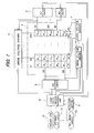
Fig. 1 , which illustrates a first embodiment of the lightening apparatus according to the presently disclosed subject matter, the lightening apparatus, that is mounted on a vehicle, includes anLED panel 1,reference voltage drivers LED panel 1, drivevoltage drivers LED panel 1, a lightdistribution control unit 8 for receiving various sense signals such as signals from aheadlamp switch 91, a high/low beam switch 92, aradar unit 10, asteering angle sensor 11, and the like directly or indirectly through other control units to control thereference voltage drivers drive voltage drivers distribution control unit 8 is constructed by a microcomputer. Thus, various light distribution patterns can be realized at theLED panel 1. - The
LED panel 1 includes LED elements P1,1, P1,2, ···, P1, 20; P2, 1, P2, 2, ···, P2, 20; ···; P5, 1, P5, 2, ···, P5, 20 in five rows, twenty columns. In more detail, as illustrated inFig. 2 , the LED elements P1, 1, P1, 2, ···, P1, 20 belonging to the first row have cathode electrodes commonly connected to a reference voltage line S1, and anode electrodes connected to the drive voltage lines X1, X2, ···, X20, respectively. Also, the LED elements P2, 1, P2, 2, ···, P2, 20 belonging to the second row have cathode electrodes commonly connected to a reference voltage line S2, and anode electrodes connected to the drive voltage lines Y1, Y2, ···, Y20, respectively. Further, the LED elements P3, 1, P3, 2, ···, P3, 20 belonging to the third row have cathode electrodes commonly connected to a reference voltage line S3, and anode electrodes connected to the drive voltage lines X1, X2, ···, X20, respectively. Further, the LED elements P4, 1, P4, 2, ···, P4, 20 belonging to the fourth row have cathode electrodes commonly connected to a reference voltage line S4, and anode electrodes connected to the drive voltage lines Z1, Z2, ···, Z20, respectively. Furthermore, the LED elements P5, 1, P5, 2, ···, P5, 20 belonging to the fifth row have cathode electrodes commonly connected to a reference voltage line S5, and anode electrodes connected to the drive voltage lines Y1, Y2, ···, Y20, respectively. - That is, the anode electrodes of the LED elements P1, 1, P1, 2, ···, P1, 20 for the first row and the anode electrodes of the LED elements P3, 1, P3, 2, ···, P3, 20 for the third row are commonly connected to the drive voltage lines X1, X2, ···, X20. Also, the anode electrodes of the LED elements P2, 1, P2, 2, ···, P2, 20 for the second row and the anode electrodes of the LED elements P5, 1, P5, 2, ···, P5, 20 for the fifth row are commonly connected to the drive voltage lines Y1, Y2, ···, Y20.
- The
reference voltage driver 2 is a multiplexing switching circuit which time-divisionally activates or switches the reference voltage lines S1 and S3 with a luminous period ratio of T1:T3=20:80 as illustrated inFig. 3 where one entire period T0=T1+T3 and each of the activated reference voltages is the ground voltage GND. Simultaneously, thedrive voltage driver 5 is operated in synchronization with the time-divisional switching of the reference voltage lines S1 and S3. That is, thedrive voltage driver 5 is driven by the voltage at the reference voltage line S1, so that thedrive voltage driver 5 generates pulse-shaped luminous drive voltages A1, A2, ···, A20 defined by their on-duty ratios for the first row during the luminous period T1, i.e.,
voltage at X1=A1
voltage at X2=A2
...
voltage at X20=A20. - Also, the
drive voltage driver 5 is driven by the voltage at the reference voltage line S3, so that thedrive voltage driver 5 generates pulse-shaped luminous drive voltages C1, C2, ···, C20 defined by their on-duty ratios for the third row during the luminous period T3, i.e.,
voltage at X1=C1
voltage at X2=C2
voltage at X20=C20. - Thus, the LED elements P1, 1, P1, 2, ···, P1, 20 for the first row and the LED elements P3, 1, P3, 2, ···, P3, 20 for the third row are time-divisionally driven by a dynamic driving method.
- The
reference voltage driver 3 is a multiplexing switching circuit which time-divisionally activates or switches the reference voltage lines S2 and S5 with a luminous period ratio of T2:T5=50:50 as illustrated inFig. 3 where T0=T2+T5 and each of the activated reference voltages is the ground voltage GND. Simultaneously, thedrive voltage driver 6 is operated in synchronization with the time-divisional switching of the reference voltage lines S2 and S5. That is, thedrive voltage driver 6 is driven by the voltage at the reference voltage line S2, so that thedrive voltage driver 6 generates pulse-shaped luminous drive voltages B1, B2, ···, B20 defined by their on-duty ratios for the second row during the luminous period T2, i.e.,
voltage at Y1=B1
voltage at Y2=B2
...
voltage at Y20=B20. - Also, the
drive voltage driver 6 is driven by the voltage at the reference voltage line S5, so that thedrive voltage driver 6 generates pulse-shaped luminous drive voltages E1, E2, ···, E20 defined by their on-duty ratios for the fifth row during the luminous period T5, i.e.,
voltage at Y1=E1
voltage at Y2=E2
...
voltage at Y20=E20. - Thus, the LED elements P2, 1, P2, 2, ···, P2, 20 for the second row and the LED elements P5, 1, P5, 2, ···, P5, 20 for the fifth row are time-divisionally driven by a dynamic driving method.
- The
reference voltage driver 4 is a simple switching circuit which activates or switches the reference voltage line S4 over the entire luminous period T0 as illustrated inFig. 3 where the activated reference voltage is the ground voltage GND. In this case, thedrive voltage driver 7 generates pulse-shaped luminous drive voltages D1, D2, ···, D20 defined by their on-duty ratios for the fourth row during the entire luminous period T0, i. e. ,
voltage at Z1=D1
voltage at Z2=D2
...
voltage at Z20=D20. - Thus, the LED elements P4, 1, P4, 2, ···, P4, 20 for the fourth row are driven by a static driving method.
- In
Fig. 3 , note that DT designates a duty ratio. - In
Fig. 4A , which is a block circuit diagram of thereference voltage driver 2 ofFig. 1 , thereference voltage driver 2 is constructed by a pulse width modulation (PWM) circuit which includeslatch circuits flop 25, andoutput amplifiers - When the PWM circuit of
Fig. 4A is activated by the lightdistribution control unit 8, first, duty ratio values corresponding to the luminous periods T1 and T3 are preset in thelatch circuits down counter 23, so that the duty ratio value of thelatch circuit 21 is loaded in thedown counter 23. Then, the clock terminal C of thedown counter 23 receives a clock signal CLK1 supplied from the lightdistribution control unit 8, so that the content of thedown counter 23 is decremented by 1 in response to each pulse of the clock signal CLK1. When thedown counter 23 underflows to generate an underflow signal from its underflow terminal U, the RS-type flip-flop 25 is set, so that the voltage at the reference voltage line S1 rises and the voltage at the reference voltage line S3 falls. Simultaneously, the duty ratio value of thelatch circuit 22 is loaded by the underflow signal of thedown counter 23 in thedown counter 24. Then, the clock terminal C of thedown counter 24 receives the clock signal CLK1 supplied from the lightdistribution control unit 8, so that the content of thedown counter 24 is decremented by 1 in response to each pulse of the clock signal CLK1. When thedown counter 24 underflows, to generate an underflow signal from its underflow terminal U, the RS-type flip-flop 25 is reset, so that the voltage at the reference voltage line S1 falls and the voltage at the reference voltage line S3 rises. Simultaneously, the duty ratio value of thelatch circuit 21 is again loaded by the underflow signal of thedown counter 24 in thedown counter 23. Thus, the above-described operations are repeated, so that the voltages at the reference voltage lines S1 and S3 as illustrated inFig. 3 can be generated. - In
Fig. 4B , which is a block circuit diagram of thereference voltage driver 3 ofFig. 1 , thereference voltage driver 2 is constructed by a PWM circuit which includeslatch circuits flop 35 andoutput amplifiers - In
Figs. 4A and 4B , after the down counters generate underflow signals, the contents thereof are retained at 0. - The operation of the PWM circuit of
Fig. 4B is similar to that of the PWM circuit ofFig. 4A . Thus, the voltages at the reference voltage lines S2 and S5 as illustrated inFig. 3 can be generated. - In
Fig. 4C , which is a block circuit diagram of thereference voltage driver 4 ofFig. 1 , thereference voltage driver 4 is constructed by an RS-type flip-flop 41 and anoutput amplifier 42 for generating a voltage at the reference voltage line S4. That is, when thereference voltage driver 4 is activated to set the RS-type flip-flop 41, theoutput amplifier 42 always lowers the voltage at the reference voltage line S4 to the ground voltage GND. - In
Fig. 5A , which is a block circuit diagram of thedrive voltage driver 5 ofFig. 1 , thedrive voltage driver 5 includes latch circuits 51-1, 51-2, ···, 51-20 for latching on-duty ratio values of the drive voltages A1, A2, ···, A20 for the LED elements P1, 1, P1, 2, ···, P1, 20 of the first row supplied from the lightdistribution control unit 8, latch circuits 52-1, 52-2, ···, 52-20 for latching on-duty ratio values of the drive voltages C1, C2, ···, C20 for the LED elements P3, 1, P3, 2, ···, P3, 20 of the third row supplied from the lightdistribution control unit 8, selectors 53-1, 53-2, ···, 53-20 for selecting the on-duty ratio values of the drive voltages A1, A2, ···, A20 of the latch circuits 51-1, 51-2, ···, 51-20 or the on-duty ratio values of the drive voltages C1, C2, ···, C20 of the latch circuits 52-1, 52-2, ···, 52-20 in accordance with the voltages at the reference voltage lines S1 and S3, drive voltage generators 54-1, 54-2, ···, 54-20 for generating the luminous drive voltages A1, A2, ···, A20 or the luminous drive voltages C1, C2, ···, C20 using the selected on-duty ratio values, and output amplifiers 55-1, 55-2, ···, 55-20 for amplifying the luminous drive voltages A1, A2, ···, A20 or C1, C2, ···, C20 to transmit them to the drive voltage lines X1, X2, ···, X20 of theLED panel 1. In this case, the drive voltage generators 54-1, 54-2, ···, 54-20 are PWM circuits for generating on-duty ratio signals whose duty ratios are determined by the selected on-duty ratio values. Thus, the LED elements P1, 1, P1, 2, ···, P1, 20 for the first row and the LED elements P3, 1, P3, 2, ···, P3, 20 for the third row can time-divisionally be operated. - In
Fig. 5B , which is a block circuit diagram of thedrive voltage driver 6 ofFig. 1 , thedrive voltage driver 6 includes latch circuits 61-1, 61-2, ···, 61-20 for latching on-duty ratio values of the drive voltages B1, B2, ···, B20 for the LED elements P2, 1, P2, 2, ···, P2, 20 of the second row supplied from the lightdistribution control unit 8, latch circuits 62-1, 62-2, ···, 62-20 for latching on-duty ratio values of the drive voltages E1, E2, ···, E20 for the LED elements P5, 1, P5, 2, ···, P5, 20 of the fifth row supplied from the lightdistribution control unit 8, selectors 63-1, 63-2, ···, 63-20 for selecting the on-duty ratio values of the drive voltages B1, B2, ···, B20 of the latch circuits 61-1, 61-2, ···, 61-20 or the on-duty ratio values of the drive voltages E1, E2, ···, E20 of the latch circuits 62-1, 62-2, ···, 62-20 in accordance with the voltages at the reference voltage lines S2 and S5, drive voltage generators 64-1, 64-2, ···, 64-20 for generating the luminous drive voltages B1, B2, ···, B20 or the luminous drive voltages E1, E2, ···, E20 using the selected on-duty ratio values, and output amplifiers 65-1, 65-2, ···, 65-20 for amplifying the luminous drive voltages B1, B2, ···, B20 or E1, E2, ···, E20 to transmit them to the drive voltage lines Y1, Y2, ···, Y20 of theLED panel 1. In this case, the drive voltage generators 64-1, 64-2, ···, 64-20 are PWM circuits for generating on-duty ratio signals whose duty ratios are determined by the selected on-duty ratio values. Thus, the LED elements P2, 1, P2, 2, ···, P2, 20 for the second row and the LED elements P5, 1, P5, 2, ···, P5, 20 for the fifth row can time-divisionally be operated. - In
Fig. 5C , which is a block circuit diagram of thedrive voltage driver 7 ofFig. 1 , thedrive voltage driver 7 includes latch circuits 71-1, 71-2, ···, 71-20 for latching on-duty ratio values of the drive voltages D1, D2, ···, D20 for the LED elements P4, 1, P4, 2, ···, P4, 20 of the fourth row supplied from the lightdistribution control unit 8, drive voltage generators 72-1, 72-2, ···, 72-20 for generating the luminous drive voltages D1, D2, ···, D20 using the on-duty ratio values of the latch circuits 71-1, 71-2, ···, 71-20, and output amplifiers 73-1, 73-2, ···, 73-20 for amplifying the luminous drive voltages D1, D2, ···, D20 to transmit them to the drive voltage lines Z1, Z2, ···, Z20 of theLED panel 1. In this case, the drive voltage generators 72-1, 72-2, ···, 72-20 are PWM circuits for generating on-duty ratio signals whose duty ratios are determined by the on-duty ratio values. Thus, the LED elements P4, 1, P4, 2, ···, P4, 20 for the fourth row can always be operated. - Each of the PWM circuits 54-1, 54-2, ···, 54-20; 64-1, 64-2, ···, 64-20; and 72-1, 72-2, ···, 72-20 has the same configuration as illustrated in
Fig. 6 , similar to those ofFigs. 4A and 4B . - In
Fig. 6 , the PWM circuit includeslatch circuits flop 85 for generating a voltage at the corresponding drive voltage line. - When the PWM circuit of
Fig. 6 is activated by the lightdistribution control unit 8, first, a duty ratio value don and an off-duty ratio value doff corresponding to one of the drive voltages are preset in thelatch circuits down counter 83, so that the on-duty ratio value don of thelatch circuit 81 is loaded in thedown counter 83. Then, the clock terminal C of thedown counter 83 receives a clock signal CLK2 supplied from the lightdistribution control unit 8, so that the content of thedown counter 83 is decremented by 1 in response to each pulse of the clock signal CLK2. In this case, the frequency of the clock signal CLK2 is preferably larger than that of the clock signal CLK1. When thedown counter 83 underflows to generate an underflow signal from its underflow terminal U, the RS-type flip-flop 85 is reset, so that the voltage at the drive voltage line falls. Simultaneously, the off-duty ratio value doff of thelatch circuit 82 is loaded by the underflow signal of thedown counter 83 in thedown counter 84. Then, the clock terminal C of thedown counter 84 receives the clock signal CLK2 supplied from the lightdistribution control unit 8, so that the content of thedown counter 84 is decremented by 1 in response to each pulse of the clock signal CLK2. When thedown counter 84 underflows to generate an underflow signal from its underflow terminal U, the RS-type flip-flop 85 is set, so that the voltage at the drive voltage line rises. Simultaneously, the duty ratio value don of thelatch circuit 81 is again loaded by the underflow signal of thedown counter 84 in thedown counter 83. Thus, the above-described operations are repeated, so that a pulse-shaped drive voltage having the on-duty ratio value don and the off-duty ratio value doff can be generated. - In
Fig. 6 , after the down counters 83 and 84 generate underflow signals, the contents thereof are retained at 0. -
Fig. 7A is a simplified block circuit diagram of the lightening apparatus ofFig. 1 , andFig. 7B is a diagram for explaining the maximum luminous intensities of the LED elements P1, 1, P1, 2, ···, P1, 20; P2, 1, P2, 2, ···, P2, 20; P3, 1, P3, 2, ···, P3, 20; P4, 1, P4, 2, ···, P4, 20; and P5, 1, P5, 2, ···, P5, 20 of theLED panel 1 ofFig. 7A . InFig. 7B , the voltages at the luminous drive voltage lines X1, X2, ···, X20; Y1, Y2, ···, Y20; and Z1, Z2, ···, Z20 have a high level such as the power supply voltage VCC with a 100% on-duty ratio. Also, assume that, when an LED element is driven over the entire period T0, the luminous intensity is 100. - The LED elements P1, 1, P1, 2, ···, P1, 20 for the first row are driven for the period T1 (=0.2·T0), so that the maximum luminous intensity of each of the LED elements P1, 1, P1,2, ···, P1,20 is 20 (=100×0.2). Therefore, the luminous intensities of the LED elements P1, 1, P1, 2, ···, P1, 20 are ranged from 0 (dark) to 20 in accordance with the on-duty ratios of the luminous drive voltages A1, A2, ···, A20.
- The LED elements P2, 1, P2, 2, ···, P2, 20 for the second row are driven for the period T2 (=0. 5 TO), so that the maximum luminous intensity of each of the LED elements P2, 1, P2, 2, ···, P2, 20 is 50 (=100×0.5). Therefore, the luminous intensities of the LED elements P2, 1, P2, 2, ···, P2, 20 are ranged from 0 (dark) to 50 in accordance with the on-duty ratios of the luminous drive voltages B1, B2, ···, B20.
- The LED elements P3, 1, P3, 2, ···, P3, 20 for the third row are driven for the period T3 (=0.8·T0), so that the maximum luminous intensity of each of the LED elements P3, 1, P3, 2, ···, P3, 20 is 80 (=100×0.8). Therefore, the luminous intensities of the LED elements P3, 1, P3, 2, ···, P3, 20 are ranged from 0 (dark) to 80 in accordance with the on-duty ratios of the luminous drive voltages C1, C2, ···, C20.
- The LED elements P4, 1, P4, 2, ···, P4, 20 for the fourth row are driven for the period T0, so that the maximum luminous intensity of each of the LED elements P4, 1, P4, 2, ···, P4, 20 is 100. Therefore, the luminous intensities of the LED elements P4, 1, P4, 2, ···, P4, 20 are ranged from 0 (dark) to 100 in accordance with the on-duty ratios of the luminous drive voltages D1, D2, ···, D20.
- The LED elements P5, 1, P5, 2, ···, P5, 20 for the fifth row are driven for the period T5 (=0.5·T0), so that the maximum luminous intensity of each of the LED elements P5, 1, P5, 2, ···, P5, 20 is 50 (=100×0.5). Therefore, the luminous intensities of the LED elements P5, 1, P5, 2, ···, P5, 20 are ranged from 0 (dark) to 50 in accordance with the on-duty ratios of the luminous drive voltages E1, E2, ···, E20.
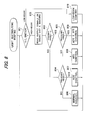
- An operation of the light
distribution control unit 8 is explained next with reference to a flowchart as illustrated inFig. 8 . This flowchart is carried out only when theheadlamp switch 91 is turned on. - First, at
step 801, it is determined whether or not the high/low (H/L)beam switch 92 is on the high-beam side or on the low-beam side. When the high/low beam switch 91 is on the high-beam side, the flow proceeds tosteps 802 to 809. Otherwise, the flow proceeds to step 810, which carries out a low-beam control. - At
step 802, the lightdistribution control unit 8 reads the output signals of theradar unit 10, thesteering angle sensor 11 and the other sensors. - Next, at
step 803, it is determined whether or not the steering angle read from thesteering angle sensor 11 is larger than a predetermined value α. Also, atsteps radar unit 10. - When the steering angle is not larger than α and no preceding vehicle is detected, the flow proceeds from
step 803 throughstep 804 to step 806 which carries out a normal high-beam control. That is, on-duty ratios don/(don + doff) of the luminous drive voltages A1, A2, ···, A20 ; B1, B2, ···, B20 ; C1, C2, ···, C20 ; D1, D2, ···, D20 ; and E1, E2, ···, E20 are calculated as illustrated inFig. 9A in accordance with the output signals of the various sensors. InFig. 9A , the on-duty ratios don/(don+doff) of the luminous drive voltages are made 1 (=100%) in a central area of theLED panel 1, while are made smaller than 1 (=100%) in right and left peripheral areas of theLED panel 1. Then, the luminous drive voltages A1, A2, ···, A20 and the luminous drive voltages C1, C2, ···, C20 are time-divisionally supplied to the luminous drive lines X1, X2, ···, X20, the luminous drive voltages B1, B2, ···, B20 and the luminous drive voltages E1, E2, ···, E20 are time-divisionally supplied to the luminous drive lines Y1, Y2, ···, Y20, and the luminous drive voltages D1, D2, ···, D20 are always supplied to the luminous drive lines Z1, Z2, ···, Z20. As a result, luminous intensities of the LED elements P1, 1, P1, 2, ···, P1, 20; P2, 1, P2, 2, ···, P2, 20 ; P3, 1, P3, 2, ···, P3, 20; P4, 1, P4, 2, ···, P4, 20; and P5, 1, P5, 2, ···, P5, 20 are realized as illustrated inFig. 9B . InFig. 9B , in a central area of theLED panel 1, the luminous intensities of the LED elements P4, 8 to P4, 13 for the fourth row are 100, and the luminous intensities of the LED elements P3, 8 to P3, 13 for the third row are 80. On the other hand, in a peripheral area of theLED panel 1, the luminous intensity is gradually decreased from 50 through 20 to 0. - When the steering angle is not larger than α and a preceding vehicle is detected, the flow proceeds from
step 803 throughstep 804 to step 807 which carries out an adaptive drive beam (ADB) control. That is, on-duty ratios don/(don+doff) of the luminous drive voltages A1, A2, ···, A20 ; B1, B2, ···, B20 ; C1, C2, ···, C20 ; D1, D2, ···, D20 ; and E1, E2, ···, E20 are calculated as illustrated inFig. 10A in accordance with the output signals of the various sensors. InFig. 10A , the on-duty ratios don/(don+doff) of the luminous drive voltages A9, A10, A11, A12; B9, B10, B11, B12 ; and C9, C10, C11, C12 for the first, second, third rows corresponding to the preceding vehicle are made 0 (=0%) in the central area of theLED panel 1 ofFig. 10A . Then, the luminous drive voltages A1, A2, ···, A20 and the luminous drive voltages C1, C2, ···, C20 are time-divisionally supplied to the luminous drive lines X1, X2, ···, X20, the luminous drive voltages B1, B2, ···, B20 and the luminous drive voltages E1, E2, ···, E20 are time-divisionally supplied to the luminous drive lines Y1, Y2, ···, Y20, and the luminous drive voltages D1, D2, ···, D20 are always supplied to the luminous drive lines Z1, Z2, ···, Z20. As a result, luminous intensity of the LED elements P1, 1, P1, 2, ···, P1, 20; P2, 1, P2, 2, ···, P2, 20; P3, 1, P3, 2, ···, P3, 20; P4, 1, P4, 2, ···, P4, 20; and P5, 1, P5, 2, ···, P5, 20 are realized as illustrated inFig. 10B . InFig. 10B , in a central area of theLED panel 1, the luminous intensities of the LED elements P4 to P4, 13 for the fourth row are 100, and the luminous intensities of the LED elements P3, 8 and P3, 13 for the third row are 80. Also, in the central area of theLED panel 1, the luminous intensities of the LED elements P1, 9 to P1, 12, P2, 9 to P2, 12, and P3, 9 to P3, 12 for the first, second and third rows are 0 to decrease the illuminance against the preceding vehicle. On the other hand, in a peripheral area of theLED panel 1, the luminous intensity is gradually decreased from 50 through 20 to 0. - When the steering angle is larger than α and no preceding vehicle is detected, the flow proceeds from
step 803 throughstep 805 to step 808 which carries out an adaptive front-lighting system (AFS) control. That is, on-duty ratios don/(don+doff) of the luminous drive voltages A1, A2, ···, A20; B1, B2, ···, B20; C1, C2, ···, C20; D1, D2, ···, D20; and E1, E2, ···, E20 are calculated as illustrated inFig. 11A in accordance with the output signals of the various sensors. InFig. 11A , when the steering direction is on the right side, the on-duty ratios don/(don+doff) of the luminous drive voltages ofFig. 9A are shifted on the right side, to substantially change the optical direction of theLED panel 1 toward the right side. Then, the luminous drive voltages A1, A2, ···, A20 and the luminous drive voltages C1, C2, ···, C20 are time-divisionally supplied to the luminous drive lines X1, X2, ···, X20, the luminous drive voltages B1, B2, ···, B20 and the luminous drive voltages E1, E2, ···, E20 are time-divisionally supplied to the luminous drive lines Y1, Y2, ···, Y20, and the luminous drive voltages D1, D2, ···, D20 are always supplied to the luminous drive lines Z1, Z2, ···, Z20. As a result, luminous intensities of the LED elements P1, 1, P1, 2, ···, P1, 20; P2, 1, P2, 2, ···, P2, 20; P3, 1, P3, 2, ···, P3, 20; P4, 1, P4, 2, ···, P4, 20; and P5, 1, P5, 2, ···, P5, 20 are realized as illustrated inFig. 11B . InFig. 11B , in a right-side central area of theLED panel 1, the luminous intensities of the LED elements P4, 10 to P4, 15 for the fourth row is 100, and the luminous intensities of the LED elements P3, 10 to P3, 15 for the third row is 80. On the other hand, in a left-side peripheral area of theLED panel 1, the luminous intensity is gradually decreased from 50 through 20 to 0, while in a right-side peripheral area of theLED panel 1, the luminous intensity is gradually decreased from 50 to 20. - When the steering angle is larger than α and a preceding vehicle is detected, the flow proceeds from
step 803 throughstep 805 to step 809 which carries out both of an adaptive drive beam (ADB) and an adaptive front-lighting system (AFS) control. That is, on-duty ratios don/(don+doff) of the luminous drive voltages A1, A2, ···, A20; B1, B2, ···, B20; C1, C2, ···, C20 ; D1, D2, ···, D20; and E1, E2, ···, E20 are calculated as illustrated inFig. 12A in accordance with the output signals of the various sensors. InFig. 12A , when the steering direction is on the right side, the on-duty ratios don/(don+doff) of the luminous drive voltages ofFig. 10A are shifted on the right side, to substantially change the optical direction of theLED panel 1 toward the right side. In addition, the on-duty ratios don/(don+doff) of the luminous drive voltages A11, A12, A13, A14; B11, B12, B13, B14; and C11, C12, C13, C14 for the first, second and third rows corresponding to the preceding vehicle are made 0 (=0%). Then, the luminous drive voltages A1, A2, ···, A20 and the luminous drive voltages C1, C2, ···, C20 are time-divisionally supplied to the luminous drive lines X1, X2, ···, X20, the luminous drive voltages B1, B2, ···, B20 and the luminous drive voltages E1, E2, ···, E20 are time-divisionally supplied to the luminous drive lines Y1, Y2, ···, Y20, and the luminous drive voltages D1, D2, ···, D20 are always supplied to the luminous drive lines Z1, Z2, ···, Z20. As a result, luminous intensities of the LED elements P1, 1, P1, 2, ···, P1, 20; P2, 1, P2, 2, ···, P2, 20; P3, 1, P3, 2, ···, P3, 20; P4, 1, P4, 2, ···, P4, 20; and P5, 1, P5, 2, ···, P5, 20 are realized as illustrated inFig. 12B . InFig. 12B , in a right-side central area of theLED panel 1, the luminous intensities of the LED elements P4, 10 to P4, 15 for the fourth row are 100, and the luminous intensities of the LED elements P3, 10 to P3, 15 for the third row are 80. Also, the luminous intensities of the LED elements P1, 11 to P1, 14, P2, 11 to P2, 14 and P3, 11 to P3, 14 are 0 to decrease the illumination against the preceding vehicle. On the other hand, in a left-side peripheral area of theLED panel 1, the luminous intensity is gradually decreased from 50 through 20 to 0, while in a right-side peripheral area of theLED panel 1, the luminous intensity is gradually decreased from 50 to 20. - At
step 810, a low-beam control similar to the normal high-beam control is carried out. Particularly, on-duty ratios of the luminous drive voltages A1, A2, ···, A20 for the first row are made 0 (0%) to decline the optical direction of theLED panel 1, so that a cut-off line is made clear. - Since the lightening apparatus of
Fig. 1 is driven by a dynamic driving method and a static driving method, the number of voltage lines including reference voltage lines and luminous voltage lines is 65 (=5+20×3). Note that if the lightening apparatus ofFig. 1 is driven by only a static driving method, the number of voltage lines is 100 (=20×5) plus the ground line. Therefore, the number of voltage lines can be decreased. Also, since one output amplifier is required for each of the voltage lines, the number of output amplifiers can be decreased to reduce the lightening apparatus in size and the power consumption thereof. - On the other hand, in the lightening apparatus of
Fig. 1 , since every two reference voltage lines are time-divisionally driven by a dynamic driving method, the luminous period for every row of theLED panel 1 can be increased as compared with those where five reference voltage lines time-divisionally driven by a dynamic driving method, thus increasing the brightness of theLED panel 1. - Still further, in the lightening apparatus of
Fig. 1 , the duty ratio T1/(T1+T3) for one time-divisional driving is different from the duty ratio T3/(T3+T5) for another time-divisional driving, areas having different luminous intensities are created in theLED panel 1. In more detail, since the maximum luminous intensities of the first row, the second row, the third row, the fourth row and the fifth row are 20, 50, 80, 100 and 50, respectively, optimum light distribution patterns for vehicle headlamps whose luminous intensities are gradually changed as illustrated inFig. 9B ,10B ,11B and12B can be realized. -
Fig. 13A is a block circuit diagram illustrating a second embodiment of the lightening apparatus according to the presently disclosed subject matter, andFig. 13B is a diagram for explaining the maximum luminous intensities of the LED elements ofFig. 13A . - In
Fig. 13A , LED elements P6, 1, P6, 2, ···, P6, 20 connected to a reference voltage line S6 and drive voltage lines V1, V2, ···, V20 are added to theLED panel 1 ofFig. 7A . Also, areference voltage driver 21 and adrive voltage driver 22 are added to the lightening apparatus ofFig. 7A . - The
reference voltage driver 3 is a multiplexing switching circuit which time-divisionally activates or switches the reference voltage lines S2 and S6 with a luminous period ratio of T2:T6=50:50 where T0=T2+T6. Simultaneously, thedrive voltage driver 6 is operated in synchronization with the time-divisional switching of the reference voltage lines S2 and S6. That is, thedrive voltage driver 6 is driven by the voltage at the reference voltage line S2, so that thedrive voltage driver 6 generates pulse-shaped luminous drive voltages B1, B2, ···, B20 defined by their on-duty ratios for the second row during the luminous period T2, i.e.,
voltage at Y1=B1
voltage at Y2=B2
...
voltage at Y20=B20. - Also, the
drive voltage driver 6 is driven by the voltage at the reference voltage line S6, so that thedrive voltage driver 6 generates pulse-shaped luminous drive voltages F1, F2, ···, F20 defined by their on-duty ratios for the sixth row during the luminous period T6, i.e.,
voltage at Y1=F1
voltage at Y2=F2
...
voltage at Y20=F20. - Thus, the LED elements P2, 1, P2, 2, ···, P2, 20 for the second row and the LED elements P6, 1, P6, 2, ···, P6, 20 for the sixth row are time-divisionally driven by a dynamic driving method.
- The
reference voltage driver 21 is a simple switching circuit, similar to thereference voltage driver 4 ofFig. 4C , which activates or switches the reference voltage line S5 over the entire luminous period T0. In this case, thedrive voltage driver 22 generates pulse-shaped luminous drive voltages E1, E2, ···, E20 defined by their on-duty ratios for the fifth row during the entire luminous period T0, i.e.,
voltage at V1=E1
voltage at V2=E2
...
voltage at V20=E20. - Thus, the LED elements P5, 1, P5, 2, ···, P5, 20 for the fifth row are driven by a static driving method.
- In
Fig. 13B , the maximum luminous intensity of each of the LED elements P1, 1, P1,2, ···, P1, 20 for the first row is 20 (=100×0.2). Therefore, the luminous intensities of the LED elements P1, 1, P1, 2, ···, P1, 20 are ranged from 0 (dark) to 20 in accordance with the on-duty ratios of the luminous drive voltages A1, A2, ···, A20. The maximum luminous intensity of each of the LED elements P2, 1, P2,2, ···, P2, 20 for the second row is 50 (=100×0.5). Therefore, the luminous intensities of the LED elements P2, 1, P2, 2, ···, P2, 20 are ranged from 0 (dark) to 50 in accordance with the on-duty ratios of the luminous drive voltages B1, B2, ···, B20. The maximum luminous intensity of each of the LED elements P3, 1, P3, 2, ···, P3, 20 for the third row is 80 (=100×0.8). Therefore, the luminous intensities of the LED elements P3, 1, P3, 2, ···, P3, 20 are ranged from 0 (dark) to 80 in accordance with the on-duty ratios of the luminous drive voltages C1, C2, ···, C20. The maximum luminous intensity of each of the LED elements P4, 1, P4, 2, ···, P4, 20 for the fourth row is 100. Therefore, the luminous intensities of the LED elements P4, 1, P4, 2, ···, P4, 20 are ranged from 0 (dark) to 100 in accordance with the on-duty ratios of the luminous drive voltages D1, D2, ···, D20. The maximum luminous intensity of each of the LED elements P5, 1, P5, 2, ···, P5, 20 for the fifth row is 100. Therefore, the luminous intensities of the LED elements P5, 1, P5, 2, ···, P5, 20 are ranged from 0 (dark) to 100 in accordance with the on-duty ratios of the luminous drive voltages E1, E2, ···, E20. The maximum luminous intensity of each of the LED elements P6, 1, P6, 2, ···, P6, 20 for the sixth row is 50 (=100×0.5). Therefore, the luminous intensities of the LED elements P6, 1, P6, 2, ···, P6, 20 are ranged from 0 (dark) to 50 in accordance with the on-duty ratios of the luminous drive voltages F1, F2, ···, F20. - Thus, according to the lightening apparatus of
Figs. 13A and 13B , the number of rows in theLED panel 1 can easily be increased. -
Fig. 14A is a block circuit diagram illustrating a third embodiment of the lightening apparatus according to the presently disclosed subject matter, andFig. 14B is a diagram for explaining the maximum luminous intensities of the LED elements ofFig. 14A . - In
Fig. 14A , thereference voltage driver 21 and thedrive voltage driver 22 ofFig. 13A are removed, and thereference voltage driver 2 and thedrive voltage driver 5 ofFig. 13A are replaced by a reference voltage driver 2' and a drive voltage driver 5' , respectively. - The reference voltage driver 2' is a multiplexing switching circuit which time-divisionally activates the reference voltage lines S1, S2 and S5 with an luminous period ratio of T1:T2:T5=10:20:70 where T0=T1+T2+T5. Simultaneously, the drive voltage driver 5' is operated in synchronization with the time-divisional switching of the reference voltage lines S1, S2 and S5. That is, the drive voltage driver 5' is driven by the voltage at the reference voltage line S1, so that the drive voltage driver 5' generates pulse-shaped luminous drive voltages A1, A2, ···, A20 defined by their on-duty ratios for the first row during the luminous period T1, i.e.,
voltage at X1=A1
voltage at X2=A2
...
voltage at X20=A20. - Also, the drive voltage driver 5' is driven by the voltage at the reference voltage line S2, so that the drive voltage driver 5' generates pulse-shaped luminous drive voltages B1, B2, ···, B20 defined by their on-duty ratios for the second row during the luminous period T2, i.e.,
voltage at X1=B1
voltage at X2=B2
...
voltage at X20=B20. - Further, the drive voltage driver 5' is driven by the voltage at the reference voltage line S5, so that the drive voltage driver 5' generates pulse-shaped luminous drive voltages E1, E2, ···, E20 defined by their on-duty ratios for the fifth row during the luminous period T5, i.e.,
voltage at X1=E1
voltage at X2=E2
...
voltage at X20=E20. - Thus, the LED elements P1, 1, P1, 2, ···, P1, 20 for the first row, the LED elements P2, 1, P2, 2, ···, P2, 20 for the second row and the LED elements P5, 1, P5, 2, ···, P5, 20 for the fifth row are time-divisionally driven by a dynamic driving method.
- The
reference voltage driver 3 is a multiplexing switching circuit which time-divisionally activates the reference voltage lines S3 and S6 with a luminous period ratio of T3:T6=80:20 where T0=T3+T6. Simultaneously, thedrive voltage driver 3 is operated in synchronization with the time-divisional switching of the reference voltage lines S3 and S6. That is, thedrive voltage driver 6 is driven by the voltage at the reference voltage line S2, so that thedrive voltage driver 6 generates pulse-shaped luminous drive voltages C1, C2, ···, C20 defined by their on-duty ratios for the third row during the luminous period T3, i.e.,
voltage at Y1=C1
voltage at Y2=C2
...
voltage at Y20=C20. - Also, the
drive voltage driver 6 is driven by the voltage at the reference voltage line S6, so that thedrive voltage driver 6 generates pulse-shaped luminous drive voltages F1, F2, ···, F20 defined by their on-duty ratios for the sixth row during the luminous period T6, i.e.,
voltage at Y1=F1
voltage at Y2=F2
...
voltage at Y20=F20. - Thus, the LED elements P3, 1, P3, 2, ···, P3, 20 for the third row and the LED elements P6, 1, P6, 2, ···, P6, 20 for the sixth row are time-divisionally driven by a dynamic driving method.
- The
reference voltage driver 4 is a simple switching circuit which activates or switches the reference voltage line S4 over the entire luminous period T0. In this case, thedrive voltage driver 7 generates pulse-shaped luminous drive voltages D1, D2, ···, D20 defined by their on-duty ratios for the fourth row during the entire luminous period T0, i.e.,
voltage at Z1=D1
voltage at Z2=D2
...
voltage at Z20=D20. - Thus, the LED elements P4, 1, P4, 2, ···, P4, 20 for the fourth row are driven by a static driving method.
- In
Fig. 14B , the maximum luminous intensity of each of the LED elements P1, 1, P1, 2, ···, P1, 20 for the first row is 10 (=100×0.1). Therefore, the luminous intensities of the LED elements P1, 1, P1, 2, ···, P1, 20 are ranged from 0 (dark) to 10 in accordance with the on-duty ratios of the luminous drive voltages A1, A2, ···, A20. The maximum luminous intensity of each of the LED elements P2, 1, P2, 2, ···, P2, 20 for the second row is 20 (=100×0.2). Therefore, the luminous intensities of the LED elements P2, 1, P2, 2, ···, P2, 20 are ranged from 0 (dark) to 20 in accordance with the on-duty ratios of the luminous drive voltages B1, B2, ···, B20. The maximum luminous intensity of each of the LED elements P3, 1, P3, 2, ···, P3, 20 for the third row is 80 (=100×0.8). Therefore, the luminous intensities of the LED elements P3, 1, P3, 2, ···, P3, 20 are ranged from 0 (dark) to 80 in accordance with the on-duty ratios of the luminous drive voltages C1, C2, ···, C20. The maximum luminous intensity of each of the LED elements P4, 1, P4, 2, ···, P4, 20 for the fourth row is 100. Therefore, the luminous intensities of the LED elements P4, 1, P4, 2, ···, P4, 20 are ranged from 0 (dark) to 100 in accordance with the on-duty ratios of the luminous drive voltages D1, D2, ···, D20. The maximum luminous intensity of each of the LED elements P5, 1, P5, 2, ···, P5, 20 for the fifth row is 70 (=100×0.7). Therefore, the luminous intensities of the LED elements P5, 1, P5, 2, ···, P5, 20 are ranged from 0 (dark) to 70 in accordance with the on-duty ratios of the luminous drive voltages E1, E2, ···, E20. The maximum luminous intensity of each of the LED elements P6, 1, P6, 2, ···, P6, 20 for the sixth row is 20 (=100×0.2). Therefore, the luminous intensities of the LED elements P6, 1, P6, 2, ···, P6, 20 are ranged from 0 (dark) to 20 in accordance with the on-duty ratios of the luminous drive voltages F1, F2, ···, F20. - In
Fig. 15 , which is a block circuit diagram of the reference voltage driver 2' ofFig. 14A , the reference voltage driver 2' is constructed by a PWM circuit which includes latch circuits 21' 22' and 23' , down counters 24' , 25' and 26' , RS-type flip-flops 27' , 28' and 29' , and output amplifiers 30', 31' and 32' for generating voltages at the reference voltage lines S1, S2 and S5. - When the PWM circuit of
Fig. 15 is activated by the lightdistribution control unit 8, first, duty ratio values corresponding to the luminous periods T1, T2 and T5 are preset in the latch circuits 21', 22' and 23' , respectively. Then, a load signal (not shown) may initially be supplied to the load terminal L of the down counter 24' , so that the duty ratio value of the latch circuit 21' is loaded in the down counter 24' . Then, the clock terminal C of the down counter 24' receives a clock signal CLK1 supplied from the lightdistribution control unit 8, so that the content of the down counter 24' is decremented by 1 in response to each pulse of the clock signal CLK1. When the down counter 24' underflows to generate an underflow signal from its underflow terminal U, the RS-type flip-flop 27' is set, so that the voltage at the reference voltage line S1 rises. Simultaneously, the duty ratio value of the latch circuit 22' is loaded by the underflow signal of the down counter 24' in the down counter 25' . Then, the clock terminal C of the down counter 25' receives the clock signal CLK1 supplied from the lightdistribution control unit 8, so that the content of the down counter 25' is decremented by 1 in response to each pulse of the clock signal CLK1. When the down counter 26' underflows to generate an underflow signal from its underflow terminal U, the RS-type flip-flop 28' is set, so that the voltage at the reference voltage line S2 rises. Simultaneously, the duty ratio value of the latch circuit 23' is loaded by the underflow signal of the down counter 25' in the down counter 26' . Then, the clock terminal C of the down counter 26' receives the clock signal CLK1 supplied from the lightdistribution control unit 8, so that the content of the down counter 26' is decremented by 1 in response to each pulse of the clock signal CLK1. When the down counter 26' underflows to generate an underflow signal from its underflow terminal U, the RS-type flip-flop 29' is set, so that the voltage at the reference voltage line S5 rises. Simultaneously, the duty ratio value of the latch circuit 21' is again loaded by the underflow signal of the down counter 26' in the down counter 24' . Thus, the above-described operations are repeated, so that the voltages at the reference voltage lines S1, S2 and S5 whose luminous period ratio of T1:T2:T5=10:20:70 can be generated. - Thus, in the lightening apparatus of
Figs. 14A and 14B , the multiplexity of one reference voltage driver is 3. However, the multiplexity per one reference voltage driver can easily be increased to the number of rows of LED elements in theLED panel 1. -
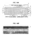
Fig. 16A is a block circuit diagram illustrating a fourth embodiment of the lightening apparatus according to the presently disclosed subject matter, andFig. 16B is a diagram for explaining the maximum luminous intensities of the LED elements ofFig. 16A . - In
Fig. 16A , thereference voltage drivers Fig. 13A are combined into one reference voltage drivers 4' , and thedrive voltage drivers Fig. 13A are combined into one drive voltage driver 7' . - The
reference voltage driver 2 is a multiplexing switching circuit which time-divisionally activates or switches the reference voltage lines S1 and S4 with luminous period ratio of T1:T4=10:90 where T0=T1+T4. Simultaneously, thedrive voltage driver 5 is operated in synchronization with the time-divisional switching of the reference voltage lines S1 and S4. That is, thedrive voltage driver 5 is driven by the voltage at the reference voltage line S1, so that thedrive voltage driver 5 generates pulse-shaped luminous drive voltages A1, A2, ···, A20 defined by their on-duty ratios for the first row during the luminous period T1, i.e.,
voltage at X1=A1
voltage at X2=A2
...
voltage at X20=A20. - Also, the
drive voltage driver 5 is driven by the voltage at the reference voltage line S4, so that thedrive voltage driver 5 generates pulse-shaped luminous drive voltages D1, D2, ···, D20 defined by their on-duty ratios for the third row during the luminous period T4, i.e.,
voltage at X1=D1
voltage at X2=D2
...
voltage at X20=D20. - Thus, the LED elements P1, 1, P1, 2, ···, P1, 20 for the first row and the LED elements P4, 1, P4, 2, ···, P4, 20 for the fourth row are time-divisionally driven by a dynamic driving method.
- The
reference voltage driver 3 is a multiplexing switching circuit which time-divisionally activates or switches the reference voltage lines S2 and S5 with a luminous period ratio of T2:T5=40:60 where T0=T2+T5. Simultaneously, thedrive voltage driver 6 is operated in synchronization with the time-divisional switching of the reference voltage lines S2 and S5. That is, thedrive voltage driver 6 is driven by the voltage at the reference voltage line S2, so that thedrive voltage driver 6 generates pulse-shaped luminous drive voltages B1, B2, ···, B20 defined by their on-duty ratios for the second row during the luminous period T2, i.e.,
voltage at Y1=B1
voltage at Y2=B2
voltage at Y20=B20. - Also, the
drive voltage driver 6 is driven by the voltage at the reference voltage line S5, so that thedrive voltage driver 6 generates pulse-shaped luminous drive voltages E1, E2, ···, E20 defined by their on-duty ratios for the fifth row during the luminous period T5, i.e.,
voltage at Y1=E1
voltage at Y2=E2
...
voltage at Y20=E20. - Thus, the LED elements P2, 1, P2, 2, ···, P2, 20 for the second row and the LED elements P5, 1, P5, 2, ···, P5, 20 for the fifth row are time-divisionally driven by a dynamic driving method.
- The reference voltage driver 4' is a multiplexing switching circuit which time-divisionally activates or switches the reference voltage lines S3 and S6 with a luminous period ratio of T3:T6=80:20 where T0=T3+T6. Simultaneously, the drive voltage driver 4' is operated in synchronization with the time-divisional switching of the reference voltage lines S2 and S5. That is, the
drive voltage driver 6 is driven by the voltage at the reference voltage line S3, so that the drive voltage driver 4' generates pulse-shaped luminous drive voltages C1, C2, ···, C20 defined by their on-duty ratios for the second row during the luminous period T2, i.e.,
voltage at Z1=C1
voltage at Z2=C2
...
voltage at Z20=C20. - Also, the drive voltage driver 4' is driven by the voltage at the reference voltage line S6, so that the
drive voltage driver 6 generates pulse-shaped luminous drive voltages F1, F2, ···, F20 defined by their on-duty ratios for the sixth row during the luminous period T6, i.e.,
voltage at Z1=F1
voltage at Z2=F2
...
voltage at Z20=F20. - Thus, the LED elements P3, 1, P3, 2, ···, P3, 20 for the third row and the LED elements P6, 1, P6, 2, ···, P6, 20 for the sixth row are time-divisionally driven by a dynamic driving method.
- In
Fig. 16B , the maximum luminous intensity of each of the LED elements P1, 1, P1, 2, ···, P1, 20 for the first row is 10 (=100 × 0.1). Therefore, the luminous intensities of the LED elements P1, 1, P1, 2) ···, P1, 20 are ranged from 0 (dark) to 10 in accordance with the on-duty ratios of the luminous drive voltages A1, A2, ···, A20. The maximum luminous intensity of each of the LED elements P2, 1, P2, 2, ···, P2,20 for the second row is 40 (=100 × 0.4). Therefore, the luminous intensities of the LED elements P2, 1, P2,2, ···, P2, 20 are ranged from 0 (dark) to 40 in accordance with the on-duty ratios of the luminous drive voltages B1, B2, ···, B20. The maximum luminous intensity of each of the LED elements P3, 1, P3, 2, ···, P3, 20 for the third row is 80 (=100 × 0.8). Therefore, the luminous intensities of the LED elements P3, 1, P3, 2, ···, P3, 20 are ranged from 0 (dark) to 80 in accordance with the on-duty ratios of the luminous drive voltages C1, C2, ···, C20. The maximum luminous intensity of each of the LED elements P4, 1, P4, 2, ···, P4, 20 for the fourth row is 90 (=100 × 0.9). Therefore, the luminous intensities of the LED elements P4, 1, P4, 2, ···, P4, 20 are ranged from 0 (dark) to 90 in accordance with the on-duty ratios of the luminous drive voltages D1, D2, ···, D20. The maximum luminous intensity of each of the LED elements P5, 1, P5, 2, ···, P5, 20 for the fifth row is 60 (=100 × 0.6). Therefore, the luminous intensities of the LED elements P5, 1, P5, 2, ···, P5, 20 are ranged from 0 (dark) to 60 in accordance with the on-duty ratios of the luminous drive voltages E1, E2, ···, E20. The maximum luminous intensity of each of the LED elements P6, 1, P6, 2, ···, P6, 20 for the sixth row is 20 (=100 × 0.2). Therefore, the luminous intensities of the LED elements P6, 1, P6, 2, ···, P6, 20 are ranged from 0 (dark) to 20 in accordance with the on-duty ratios of the luminous drive voltages F1, F2, ···, F20. - Thus, according to the lightening apparatus of
Figs. 16A and 16B , all the reference voltage drivers can be constructed by multiplexing switching circuits. As a result, the number of voltage lines can be decreased as compared with that ofFigs. 13A and 13B . -
Fig. 17A is a block circuit diagram illustrating a fifth embodiment of the lightening apparatus according to the presently disclosed subject matter, andFig. 17B is a diagram for explaining the maximum luminous intensities of the LED elements ofFig. 17A . - In
Fig. 17A , theLED panel 1 ofFig. 7A is divided into a left-side LED portion 1L formed by the LED elements P1, 1, P1, 2, P1, 3, P1, 4; P2, 1, P2, 2, P2, 3, P2, 4; ··· ; and P5, 1, P5, 2, P5, 3, P5, 4, a center-side LED portion 1C formed by the LED elements P1, 5, P1, 6, ···, P1, 16; P2, 5, P2, 6, ···, P2, 16; ··· ; P5, 5, P5, 6, ···, P5, 16, and a right-side LED portion 1R formed by the LED elements P1, 17, P1, 18, P1, 19, P1, 20; P2, 17 P2, 18, P2, 18, P2, 20; ···; and P5, 17, P5, 18, P5, 19, P5, 20. - The center-
side LED portion 1C is obtained by reducing theLED panel 1 ofFig. 7A . That is, the center-side LED portion 1C can be operated byreference voltage drivers reference voltage drivers Fig. 7A , and drivevoltage drivers drive voltage drivers Fig. 7A . Therefore, the description on the operation of the center-side LED portion 1C is omitted. - The left-
side LED portion 1L is explained next in detail. - The cathode electrodes of the LED elements P1, 1, P1, 2, P1, 3, P1, 4; P 2, 1, P2, 2, P2, 3, P2, 4; ··· ; and P5, 1, P5, 2, P5, 3, P5, 4 are connected to reference voltage lines S1L, S2L, S3L, S4L and S5L, respectively. On the other hand, the anode electrodes of the LED elements P1, 1, P2, 1, P3, 1, P4, 1, P5, 1; P1, 2, P2, 2, P3, 2, P4, 2; P1, 3, P2, 3, P3, 3, P4, 3; P1, 4, P2,4, P3, 4, P4, 4 are connected to drive voltage lines L1, L2, L3, L4, respectively. A
reference voltage driver 2L supplies reference voltages such as the ground voltage GND to the reference voltage lines S1L, S2L, S3L, S4L and S5L, while adrive voltage driver 5L supplies luminous drive voltages to the drive voltage lines L1, L2, L3 and L4. - The
reference voltage driver 2L is a multiplexing switching circuit which time-divisionally activates or switches the reference voltage lines S1L, S2L, S3L, S4L and S5L with luminous period ratio of T1L:T2L:T3L:T4L:T5L=20:20: 20:20:20 where T0=T1L+T2L+T3L+T4L+T5L. Simultaneously, thedrive voltage driver 5L is operated in synchronization with the time-divisional switching of the reference voltage lines S1L, S2L, S3L, S4L and S5L. That is, thedrive voltage driver 5L is driven by the voltage at the reference voltage line S1L, so that thedrive voltage driver 5L generates pulse-shaped luminous drive voltages A1, A2, A3 and A4 defined by their on-duty ratios for the first row during the luminous period T1L, i. e.,
voltage at L1=A1
voltage at L2=A2
voltage at L3=A3
voltage at L4=A4. - Also, the
drive voltage driver 5L is driven by the voltage at the reference voltage line S2L, so that thedrive voltage driver 5L generates pulse-shaped luminous drive voltages B1, B2, B3 and B4 defined by their on-duty ratios for the second row during the luminous period T2L, i.e.,
voltage at L1=B1
voltage at L2=B2
voltage at L3=B3
voltage at L4=B4. - Further, the
drive voltage driver 5L is driven by the voltage at the reference voltage line S3L, so that thedrive voltage driver 5L generates pulse-shaped luminous drive voltages C1, C2, C3 and C4 defined by their on-duty ratios for the third row during the luminous period T3L, i.e.,
voltage at L1=C1
voltage at L2=C2
voltage at L3=C3
voltage at L4=C4. - Furthermore, the
drive voltage driver 5L is driven by the voltage at the reference voltage line S4L, so that thedrive voltage driver 5L generates pulse-shaped luminous drive voltages D1, D2, D3 and D4 defined by their on-duty ratios for the fourth row during the luminous period T4L, i.e.,
voltage at L1=D1
voltage at L2=D2
voltage at L3=D3
voltage at L4=D4. - Still further, the
drive voltage driver 5L is driven by the voltage at the reference voltage line S5L, so that thedrive voltage driver 5L generates pulse-shaped luminous drive voltages E1, E2, E3 and E4 defined by their on-duty ratios for the fifth row during the luminous period T5L, i.e.,
voltage at L1=E1
voltage at L2=E2
voltage at L3=E3
voltage at L4=E4. - Thus, the LED elements P1, 1, P1, 2, P1, 3, P1, 4 for the first row, the LED elements P2, 1, P2, 2, P2, 3, P2, 4 for the second row, the LED elements P3, 1, P3, 2, P3, 3, P3, 4 for the third row, the LED elements P4, 1, P4, 2, P4, 3, P4, 4 for the fourth row, and the LED elements P5, 1, P5, 2, P5, 3, P5, 4 for the fifth row are time-divisionally driven by a dynamic driving method.
- In
Fig. 17B , the maximum luminous intensity of each of the LED elements P1, 1, P1, 2, P1, 3, P1, 4 for the first row is 20 (=100 × 0.2). Therefore, the luminous intensities of the LED elements P1, 1, P1, 2, P1, 3, P1, 4 are ranged from 0 (dark) to 20 in accordance with the on-duty ratios of the luminous drive voltages A1, A2, A3, A4. The maximum luminous intensity of each of the LED elements P2, 1, P2, 2, P2, 3, P2, 4 for the second row is 20 (=100X0.2). Therefore, the luminous intensities of the LED elements P2, 1, P2, 2, P2, 3, P2, 4 are ranged from 0 (dark) to 20 in accordance with the on-duty ratios of the luminous drive voltages B1, B2, B3, B4. The maximum luminous intensity of each of the LED elements P3, 1, P3, 2, P3, 3, P3, 4 for the third row is 20 (=100 × 0.2). Therefore, the luminous intensities of the LED elements P3, 1, P3, 2, P3, 3, P3, 4 are ranged from 0 (dark) to 20 in accordance with the on-duty ratios of the luminous drive voltages C1, C2, C3, C4. The maximum luminous intensity of each of the LED elements P4, 1, P4, 2, P4, 3, P4, 4 for the fourth row is 20 (=100 × 0.2). Therefore, the luminous intensities of the LED elements P4, 1, P4, 2, P4, 3, P4, 4 are ranged from 0 (dark) to 20 in accordance with the on-duty ratios of the luminous drive voltages D1, D2, D3, D4. The maximum luminous intensity of each of the LED elements P5, 1, P5, 2, P5, 3, P5, 4, for the fifth row is 20 (=100 × 0.2). Therefore, the luminous intensities of the LED elements P5, 1, P5, 2, P5, 3, P5, 4 are ranged from 0 (dark) to 20 in accordance with the on-duty ratios of the luminous drive voltages E1, E2, E3, E4. - The right-
side LED portion 1R is explained next in detail. - The cathode electrodes of the LED elements P1, 17, P1, 18, P1, 19, P1, 20; P2, 17, P2, 18, P2, 19, P2, 20; and P5, 17, P5, 18, P5, 19, P5, 20 are connected to reference voltage lines S1R, S2R, S3R, S4R and S5R, respectively. On the other hand, the anode electrodes of the LED elements P1, 17, P2, 17, P3, 17, P4, 17, P5, 17; P1, 18, P2, 18, P3, 18, P4, 18; P1, 19, P2, 19, P3, 19, P4, 19; P1, 20, P2, 20, P3, 20, P4, 20 are connected to drive voltage lines R1, R2, R3, R4, respectively. A
reference voltage driver 2R supplies reference voltages such as the ground voltage GND to the reference voltage lines S1R, S2R, S3R, S4R and S5R, while adrive voltage driver 5R supplies luminous drive voltages to the drive voltage lines R1, R2, R3 and R4. - The
reference voltage driver 2R is a multiplexing switching circuit which time-divisionally activates or switches the reference voltage lines S1R, S2R, S3R, S4R and S5R with luminous period ratio of T1R:T2R:T3R:T4R:T5R=20:20: 20:20:20 where T0=T1R+T2R+T3R+T4R+T5R. Simultaneously, thedrive voltage driver 5R is operated in synchronization with the time-divisional switching of the reference voltage lines S1R, S2R, S3R, S4R and S5R. That is, thedrive voltage driver 5R is driven by the voltage at the reference voltage line S1R, so that thedrive voltage driver 5R generates pulse-shaped luminous drive voltages A17, A18, A19 and A20 defined by their on-duty ratios for the first row during the luminous period T1R, i.e.,
voltage at R17=A17
voltage at R18=A18
voltage at R19=A19
voltage at R20=A20. - Also, the
drive voltage driver 5R is driven by the voltage at the reference voltage line S2R, so that thedrive voltage driver 5R generates pulse-shaped luminous drive voltages B17, B18, B19 and B20 defined by their on-duty ratios for the second row during the luminous period T2R, i.e.,
voltage at R17=B17
voltage at R18=B18
voltage at R19=B19
voltage at R20=B20 - Further, the
drive voltage driver 5R is driven by the voltage at the reference voltage line S3R, so that thedrive voltage driver 5R generates pulse-shaped luminous drive voltages C17, C18, C19 and C20 defined by their on-duty ratios for the third row during the luminous period T3R, i.e.,
voltage at R17=C17
voltage at R18=C18
voltage at R19=C19
voltage at R20=C20. - Furthermore, the
drive voltage driver 5R is driven by the voltage at the reference voltage line S4R, so that thedrive voltage driver 5R generates pulse-shaped luminous drive voltages D17, D18, D19 and D20 defined by their on-duty ratios for the fourth row during the luminous period T4R, i.e.,
voltage at R17=D17
voltage at R18=D18
voltage at R19=D19
voltage at R20=D20. - Still further, the
drive voltage driver 5R is driven by the voltage at the reference voltage line S5R, so that thedrive voltage driver 5R generates pulse-shaped luminous drive voltages E17, E18, E19 and E20 defined by their on-duty ratios for the fifth row during the luminous period T5R, i.e.,
voltage at R17=E17
voltage at R18=E18
voltage at R19=E19
voltage at R20=E20. - Thus, the LED elements P1, 17, P1, 18, P1, 19, P1, 20 for the first row, the LED elements P1, 17, P1, 18, P2, 19, P2, 20 for the second row, the LED elements P3, 17, P3, 18, P3, 19, P3, 20 for the third row, the LED elements P4, 17, P4, 18, P4, 19, P4, 20 for the fourth row, and the LED elements P5, 17, P5, 18, P5, 19, P5, 20 for the fifth row are time-divisionally driven by a dynamic driving method.
- In
Fig. 17B , the maximum luminous intensity of each of the LED elements P1, 17, P1, 18, P1, 19, P1, 20 for the first row is 20 (=100 × 0.2). Therefore, the luminous intensities of the LED elements P1, 17, P1, 18, P1, 19, P1, 20 are ranged from 0 (dark) to 20 in accordance with the on-duty ratios of the luminous drive voltages A17, A18, A19, A20. The maximum luminous intensity of each of the LED elements P2, 17, P2, 18, P2, 19, P2, 20 for the second row is 20 (=100X0.2). Therefore, the luminous intensities of the LED elements P2, 17, P2, 18, P2, 19, P2, 20 are ranged from 0 (dark) to 20 in accordance with the on-duty ratios of the luminous drive voltages B17, B18, B19, B20. The maximum luminous intensity of each of the LED elements P3, 17, P3, 18, P3, 19, P3, 20 for the third row is 20 (=100 × 0.2) . Therefore, the luminous intensities of the LED elements P3, 17, P3, 18, P3, 19, P3, 20 are ranged from 0 (dark) to 20 in accordance with the on-duty ratios of the luminous drive voltages C17, C18, C19, C20. The maximum luminous intensity of each of the LED elements P4, 17, P4, 18, P4, 19, P4, 20 for the fourth row is 20 (=100 × 0.2). Therefore, the luminous intensities of the LED elements P4, 17, P4, 18, P4, 19, P4, 20 are ranged from 0 (dark) to 20 in accordance with the on-duty ratios of the luminous drive voltages D17, D18, D19, D20. The maximum luminous intensity of each of the LED elements P5, 17, P5, 18, P5, 19, P5, 20 for the fifth row is 20 (=100 X0.2). Therefore, the luminous intensities of the LED elements P5, 17, P5, 18, P5, 19, P5, 20 are ranged from 0 (dark) to 20 in accordance with the on-duty ratios of the luminous drive voltages E17, E18, E19, E20. - Thus, according to the lightening apparatus of
Figs. 17A and 17B , in the left-side LED portion 1L and the right-side LED portion 1R, the luminous intensities of the LED elements are made uniformly low. - In
Fig. 17A , note that the operation of thereference voltage driver 2L can be synchronized with that of thereference voltage driver 2R. In this case, one of thereference voltage drivers -
Fig. 18A is a block circuit diagram illustrating a sixth embodiment of the lightening apparatus according to the presently disclosed subject matter, andFig. 18B is a diagram for explaining the maximum luminous intensities of the LED elements ofFig. 18A . - In
Fig. 18A , anLED panel 1 is divided into a center-side LED portion 1C formed by LED elements Q1, 4, Q1, 5, ···, Q1, 13; Q2, 4, Q2, 5, ···, Q2, 13; ··· ; Q6, 4, Q6, 5, ··· , Q6, 13, an outer left-side LED portion 1L1 formed by LED elements S1, 1, S1, 2; S2, 1, S2, 2; S3, 1, S3, 2 and R4, 1, R4, 2, an inner left-side LED portion 1L2 formed by LED elements Q1, 3, Q2, 3, Q3, 3 and P4, 3, an outer right-side LED portion 1R1 formed by LED elements S1, 15, S1, 16; S2, 15, S2, 16; S3, 15, S3, 16 and R4, 15, R4, 16, an inner right-side LED portion 1R2 formed by LED elements Q1, 14, Q2, 14, Q3, 14 and P4, 14. - In
Fig. 18A , each of the LED elements Q1, 3, Q1, 4, ···, Q1, 14; Q2, 3, Q2, 14; Q3, 3, Q3, 14 has a longitudinal size twice that of the LED elements P2, 4, P2, 5, ···, P2, 13; P3, 4, P3, 5, ···, P3, 13, P4, 4, P4, 5, ···, P4, 13 ; P5, 4, P5, 5, ···, P5, 13 ; P6, 4, P6, 5, ···, P6, 13 ; P4, 3 and P4, 14, while each of the LED elements R4, 1, R4, 2, R4, 15 and R4, 16 have a traverse size twice that of the above-mentioned LED elements P2, 4, P2, 5, ···, P2, 13 and the like. Therefore, the area of each of the LED elements Q1, 3, Q1, 4, ··· and the LED elements R4, 1, R4, 2, ··· is twice that of each of the LED elements P2, 4, P2, 5, ···, - The center-
side LED portion 1C is also obtained by reducing theLED panel 1 ofFig. 7A . That is, the center-side LED portion 1C can be operated byreference voltage drivers reference voltage drivers Fig. 7A , and drivevoltage drivers drive voltage drivers Fig. 7A . Therefore, the description on the operation of the center-side LED portion 1C is omitted. - Also, each of the LED elements S1, 1, S1, 2, S1, 15, S1, 16; S1, 1, S2, 2, S2, 15, S2, 16; S3, 1, S3, 2, S3, 15, S3, 16 has a longitudinal size twice those of the above-mentioned LED elements P2, 4, P2, 5, ··· and a traverse size twice those of the above-mentioned LED elements P2, 4, P2, 5, ···, P2, 13 and the like. Therefore, the area of each of the LED elements S1, 1, S1, 2, ··· is four times that of each of the LED elements P2, 4, P2, 5, ···,
- The outer left-side LED portion 1L1 is explained next in detail.
- The cathode electrodes of the LED elements S1, 1 and S1, 2 are connected to a reference voltage line S1L, and the cathode electrodes of the LED elements S2, 1 and S2, 2 are connected to a reference voltage line S2L. The reference voltage lines S1L and S2L are time-divisionally activated by a
reference voltage driver 2L with a luminous period ratio of 50:50. On the other hand, the anode electrodes of the LED elements S1, 1, S2, 1 and S1, 2, S2, 2 are connected to drive voltage lines L1 and L2, respectively, which are driven by adrive voltage driver 5L. Thus, the LED elements S1, 1 and S1, 2 for the first row and the LED elements S2, 1 and S2, 2 for the second row are time-divisionally driven by a dynamic driving method. - The cathode electrodes of the LED elements S3, 1 and S3, 2 are connected to a reference voltage line S3L, and the cathode electrodes of the LED elements S4, 1 and S4, 2 are connected to a reference voltage line S4L. The reference voltage lines S3L and S4L are time-divisionally activated by a
reference voltage driver 3L with a luminous period ratio of 60:40. On the other hand, the anode electrodes of the LED elements S3, 1, S4, 1 and S3, 2, S4, 2 are connected to drive voltage lines L3 and L4, respectively, which are driven by adrive voltage driver 6L. Thus, the LED elements S3, 1 and S3, 2 for the third row and the LED elements S4, 1 and S4, 2 for the fourth row are time-divisionally driven by a dynamic driving method. - The inner left-side LED portion IL2 is explained next in detail.
- The cathode electrodes of the LED elements Q1, 3, Q2, 3, Q3, 3 and P4, 3 are connected to reference voltage line S1L', S2L', S3L' and S4L' , respectively, which are time-divisionally activated by a
reference voltage driver 4L with a luminous period ratio of 30:30:30:10. On the other hand, the anode electrodes of the LED elements Q1, 3, Q2, 3, Q3, 3 and P4, 3 are connected to a drive voltage lines L5 which is driven by adrive voltage driver 7L. Thus, the LED elements Q1, 3, Q2, 3, Q3, 3 and P4, 3 for the first, second, third and fourth rows are time-divisionally driven by a dynamic driving method. - The outer right-side LED portion 1R1 is explained next in detail.
- The cathode electrodes of the LED elements S1, 15 and S1, 16 are connected to a reference voltage line S1R, and the cathode electrodes of the LED elements S2, 15 and S2, 16 are connected to a reference voltage line S2R. The reference voltage lines S1R and S2R are time-divisionally activated by a
reference voltage driver 2R with a luminous period ratio of 50:50. On the other hand, the anode electrodes of the LED elements S1, 15, S2, 15 and S1, 16, S2, 16 are connected to drive voltage lines R1 and R2, respectively, which are driven by adrive voltage driver 5R. Thus, the LED elements S1, 15 and S1, 16 for the first row and the LED elements S2, 15 and S2, 16 for the second row are time-divisionally driven by a dynamic driving method. - The cathode electrodes of the LED elements S3, 15 and S3, 16 are connected to a reference voltage line S3R, and the cathode electrodes of the LED elements S4, 15 and S4, 16 are connected to a reference voltage line S4R. The reference voltage lines S3R and S4R are time-divisionally activated by a
reference voltage driver 3R with a luminous period ratio of 60:40. On the other hand, the anode electrodes of the LED elements S3, 15, S4, 15 and S3, 16, S4, 16 are connected to drive voltage lines R3 and R4, respectively, which are driven by adrive voltage driver 6R. Thus, the LED elements S3, 15 and S3, 16 for the third row and the LED elements S4, 15 and S4, 16 for the fourth row are time-divisionally driven by a dynamic driving method. - The inner right-side LED portion 1R2 is explained next in detail.
- The cathode electrodes of the LED elements Q1, 14, Q2, 14, Q3, 14 and P4, 14 are connected to reference voltage line S1R', S2R', S3R'and S4R', respectively, which are time-divisionally activated by a
reference voltage driver 4R with a luminous period ratio of 30:30:30:10. On the other hand, the anode electrodes of the LED elements Q1, 14, Q2, 14, Q3, 14 and P4, 14 are connected to a drive voltage lines R5 which is driven by adrive voltage driver 7R. Thus, the LED elements Q1, 14, Q2, 14, Q3, 14 and P4, 14 for the first, second, third and fourth rows are time-divisionally driven by a dynamic driving method. - In the left-side LED portions 1L1 and 1L2 and the right-side LED portions 1R1 and 1R2 of
Fig. 18B , the maximum luminous intensities of the LED elements S1, 1, S1, 2, Q1, 3, Q1, 14, S1, 15 and S1, 16 for the first row are 50, 50, 30, 30, 50 and 50, respectively. Also, the maximum luminous intensities of the LED elements S2, 1, S2, 2, Q2, 3, Q2, 14, S2, 15 and S2, 16 for the second row are 50, 50, 30, 30, 50 and 50, respectively. Further, the maximum luminous intensities of the LED elements S3, 1, S3, 2, Q3, 3, Q3, 14, S3, 15 and S3, 16 for the third row are 60, 60, 30, 30, 60 and 60, respectively. Furthermore, the maximum luminous intensities of the LED elements R4, 1, R4, 2, P4, 3, P4, 14, R4, 15 and R4, 16 for the fourth row are 40, 40, 10, 10, 40 and 40, respectively. - Thus, according to the sixth embodiment, the LED elements can have different sizes.
- In
Fig. 18A , note that the operation of thereference voltage driver 2L can be synchronized with that of thereference voltage driver 2R. In this case, one of thereference voltage drivers reference voltage driver 3L can be synchronized with that of thereference voltage driver 3R. In this case, one of thereference voltage drivers reference voltage driver 4L can be synchronized with that of thereference voltage driver 4R. In this case, one of thereference voltage drivers - In the above-described embodiments, the reference voltage drivers are connected to the cathode electrodes of the LED elements and the drive voltage drivers are connected to the anode electrodes of the LED elements; however, the reference voltage drivers can be connected to the anode electrodes of the LED elements and the drive voltage drivers can be connected to the cathode electrodes of the LED elements. In this case, the reference voltage drivers activate the reference voltage lines by supplying positive voltages such as the power supply voltage VCC thereto, while the on-duty ratio voltage of the drive voltage drivers is the low voltage such as the ground voltage.
- Also, in the above-described embodiments, the LED panel is constructed by the LED elements in a 5 rows × 20 column matrix or the like; however, the LED panel can be in other matrixes having "m" rows and "n" columns where "m" is an integer larger than 2 and "n" is a positive integer.
- Further, in the above-described embodiments, the LED elements can be replaced by organic or inorganic electro-luminescense (EL) elements.
- Furthermore, the lightening apparatus according to the presently disclosed subject matter can be applied to a vehicle headlamp of a direct-projection type, a reflection type or the like.
- It will be apparent to those skilled in the art that various modifications and variations can be made in the presently disclosed subject matter without departing from the spirit or scope of the presently disclosed subject matter. Thus, it is intended that the presently disclosed subject matter covers the modifications and variations of the presently disclosed subject matter provided they come within the scope of the appended claims and their equivalents. All related or prior art references described above and in the Background section of the present specification are hereby incorporated in their entirety by reference.
Claims (9)
- A lightening apparatus comprising:a plurality of light-emitting elements (P1, 1, P1, 2, ··· ) arranged in a matrix having "m" rows, "n" columns where "m" is an integer larger than 2 and "n" is a positive integer;at least two first reference voltage lines (S2, S5) ;"m" first drive voltage lines (Y1, Y2, ···) wherein one of said light-emitting elements (P2, 1, P2, 2, ···) is located at each intersection between said first reference voltage lines (S2, S5) and said first drive voltage lines (Y1, Y2, ···);a first reference voltage driver (3), connected to said first reference voltage lines (S2, S5) and adapted to time-divisionally switch said first reference voltage lines (S2, S5);a first drive voltage driver (6), connected to said first drive voltage lines (Y1, Y2, ···) and adapted to supply first luminous drive voltages (B1, B2, ··· ; E1, E2, ···) to said first drive voltage lines (Y1, Y2, ···) in synchronization with time-divisional switching of said first reference voltage lines (S2, S5);at least one second reference voltage line (S1, S3; S4);"m"second drive voltage lines (X1, X2, ··· ; Z1, Z2, ···) wherein one of said light-emitting elements (P1, 1, P1, 2, ···, P3, 1, P3, 2, ···; P4, 1, P4, 2, ···) is located at each intersection between said second reference voltage line (S1, S3; S4) and said second drive voltage lines (X1, X2, ··· ; Z1, Z2, ···);a second reference voltage driver (2, 4) connected to said second reference voltage line (S1, S3; S4) and adapted to switch said second reference voltage line (S1, S3; S4); anda second drive voltage driver (5, 7), connected to said second drive voltage lines (X1, X2, ··· ; Z1, Z2, ··· ) and adapted to supply second luminous drive voltages (A1, A2, ··· , C1, C2, ··· ; D1, D2, ···) to said second drive voltage lines (X1, X2, ··· ; Z1, Z2, ···) in synchronization with switching of said second reference voltage line (S1, S3; S4).
- The lightening apparatus as set forth in claim 1, wherein said second reference voltage line (S1, S3; S4) is interposed between said first reference voltage lines (S2, S5).
- The lightening apparatus as set forth in claim 1, wherein said at least one second reference voltage line is defined as at least two second reference voltage lines (S1, S3),
said second reference voltage driver (2) being adapted to time-divisionally switch said second reference voltage lines (S1, S3),
said second drive voltage driver (5) being adapted to supply said second luminous drive voltages (A1, A2, ··· ; C1, C2, ···) to said second drive voltage lines (X1, X2, ···) in synchronization with time-divisional switching of said second reference voltage lines (S1, S3). - The lightening apparatus as set forth in claim 1, wherein said second reference voltage driver (4) is adapted to always activate said second reference voltage line (S4), and wherein said second drive voltage driver (7) is adapted to supply said second luminous drive voltages (D1, D2, ···) to said second voltage lines (Z1, Z2, ···).
- The lightening apparatus as set forth in claim 1, further comprising a light distribution control unit (8) connected to said first and second reference voltage drivers (2, 3, 4) and said first and second drive voltage drivers (5, 6, 7) and adapted to preset time-divisional ratios for switching said first reference voltage lines (S2, S5) in said first reference voltage driver (3) and a time-divisional ratio for switching said second reference voltage line (S1, S3; S4) in said second reference voltage driver (2, 4) and adapted to preset on-duty ratios corresponding to said first luminous drive voltages (B1, B2, ··· ; E1, E2, ···) in said first drive voltage driver (3) and on-duty ratios corresponding to said second luminous drive voltages (A1, A2, ···, C1, C2, ···; D1, D2, ···) in said second drive voltage driver (2, 4).
- The lightening apparatus as set forth in claim 1, being applied to a headlamp in a vehicle, wherein said light distribution control unit (8) comprises;
means for determining whether or not a preceding vehicle is detected; and
means for carrying out an adaptive drive beam control to calculate the on-duty ratios corresponding to said first and second drive voltages (A1, A2, ··· ; B1, B2, ··· ; C1, C2, ··· ; D1, D2, ··· ; E1, E2, ···) to substantially decrease luminance against said preceding vehicle, when it is determined that said preceding vehicle is detected. - The lightening apparatus as set forth in claim 1, being applied to a headlamp in a vehicle, wherein said light distribution control unit (8) comprises;
means for determining whether or not a steering angle is larger than a predetermined value; and
means for carrying out an adaptive front-lighting system control to calculate the on-duty ratios corresponding to said first and second drive voltages (A1, A2, ···; B1, B2, ··· ; C1, C2, ···; D1, D2, ···; E1, E2, ···) to substantially change an optical direction of said light-emitting elements (P1, 1, P1, 2, ···), when it is determined that said steering angle is larger than said predetermined value. - The lightening apparatus as set forth in claim 1, further comprising:a plurality of left-side light-emitting elements (1L, 1L1, 1L2) provided adjacently on a left-side of said light-emitting elements (1C);left-side reference voltage lines (S1L, S2L, ···, S1L' , SLL' , ···) ;at least one left-side drive voltage line (L1, ···), wherein one of said left-side light-emitting elements (1L) is located at each intersection between said left-side reference voltage lines (S1L, S2L, ···) and said left-side drive voltage line (L1, ···);at least one left-side reference voltage driver (2L, 3L, 4L), connected to said left-side reference voltage lines (S1L, S2L, ···) and adapted to time-divisionally switch said left-side reference voltage lines (S1L, S2L, ···, S1L', S2L' , ···);at least one left-side drive voltage driver (5L, 6L, 7L), connected to said left-side drive voltage line (L1, ···) and adapted to supply left-side luminous drive voltages to said left-side drive voltage line (L1, ···) in synchronization with time-divisional switching of said left-side reference voltage lines (S1L, S2L, ···, S1L', S2L', ···);a plurality of right-side light-emitting elements (1R, 1R1, 1R2) provided adjacently on a right-side of said light-emitting elements (1C);right-side reference voltage lines (S1R, S2R, ···, S1R', S2R', ···);at least one right-side drive voltage line (R17, ···), wherein one of said right-side light-emitting elements (1R) is located at each intersection between said right-side reference voltage lines (S1R, S2R, ···) and said right-side drive voltage line (R1, ···);a right-side reference voltage driver (2R, 3R, 4R), connected to said right-side reference voltage lines (S1R, S2R, ···) and adapted to time-divisionally switch said right-side reference voltage lines (S1R, S2R, ···, S1R' , S2R' , ···); andat least one right-side drive voltage driver (5R, 6R, 7R), connected to said right-side drive voltage line (R17, ···) and adapted to supply right-side luminous drive voltages to said right-side drive voltage line (R1, ···) in synchronization with time-divisional switching of said right-side reference voltage lines (S1R, S2R, ···, S1R' , S2R' , ···).
- The lightening apparatus as set forth in claim 8, wherein at least one of said left-side light-emitting elements (1L, 1L1, 1L2) and at least one of said right-side light-emitting elements (1R, 1R1, 1R2) are larger than said light-emitting elements (P2, 4, P2, 5, ···).
Applications Claiming Priority (1)
| Application Number | Priority Date | Filing Date | Title |
|---|---|---|---|
| JP2014031646A JP6282484B2 (en) | 2014-02-21 | 2014-02-21 | Light emitting device |
Publications (3)
| Publication Number | Publication Date |
|---|---|
| EP2911478A2 true EP2911478A2 (en) | 2015-08-26 |
| EP2911478A3 EP2911478A3 (en) | 2015-12-09 |
| EP2911478B1 EP2911478B1 (en) | 2018-12-26 |
Family
ID=52813880
Family Applications (1)
| Application Number | Title | Priority Date | Filing Date |
|---|---|---|---|
| EP15155292.4A Active EP2911478B1 (en) | 2014-02-21 | 2015-02-16 | Lightening apparatus having matrix-arranged light-emitting elements |
Country Status (3)
| Country | Link |
|---|---|
| US (1) | US9560706B2 (en) |
| EP (1) | EP2911478B1 (en) |
| JP (1) | JP6282484B2 (en) |
Cited By (5)
| Publication number | Priority date | Publication date | Assignee | Title |
|---|---|---|---|---|
| EP3026705A1 (en) * | 2014-11-25 | 2016-06-01 | Stanley Electric Co., Ltd. | Light-emitting diode apparatus |
| CN106541886A (en) * | 2016-10-26 | 2017-03-29 | 江苏金米智能科技有限责任公司 | A kind of headlight for vehicle light lamp automatic switching control system based on positioning |
| EP3182801A1 (en) * | 2015-12-18 | 2017-06-21 | Stanley Electric Co., Ltd. | Lighting device for vehicle |
| EP3608172A4 (en) * | 2017-04-04 | 2020-12-02 | Koito Manufacturing Co., Ltd. | Vehicle lamp fixture |
| EP3672369B1 (en) * | 2018-12-17 | 2022-10-05 | Valeo Vision | Method for controlling a light pattern and automotive lighting device |
Families Citing this family (8)
| Publication number | Priority date | Publication date | Assignee | Title |
|---|---|---|---|---|
| JP6935536B2 (en) * | 2015-12-18 | 2021-09-15 | スタンレー電気株式会社 | Vehicle lighting |
| JP6659436B2 (en) * | 2016-04-20 | 2020-03-04 | スタンレー電気株式会社 | Vehicle lighting method and vehicle lamp |
| FR3065822B1 (en) * | 2017-04-28 | 2020-08-28 | Valeo Vision | METHOD AND SYSTEM FOR CONTROL OF ELECTRIC CURRENT WITHIN A SEMICONDUCTOR LIGHT SOURCE DEFINING AT LEAST TWO DISTINCT LIGHT EMISSION ZONES |
| JP6988181B2 (en) * | 2017-06-15 | 2022-01-05 | 市光工業株式会社 | Vehicle lighting |
| JP7117921B2 (en) * | 2018-07-06 | 2022-08-15 | パイオニア株式会社 | light emitting module |
| CN109782965B (en) * | 2019-01-23 | 2022-09-27 | 京东方科技集团股份有限公司 | Touch display substrate and display device |
| JP2020191269A (en) * | 2019-05-24 | 2020-11-26 | スタンレー電気株式会社 | Vehicular lighting tool |
| EP4159540A4 (en) * | 2020-05-29 | 2024-04-10 | Koito Mfg Co Ltd | Vehicle lighting system |
Citations (1)
| Publication number | Priority date | Publication date | Assignee | Title |
|---|---|---|---|---|
| JP2013054849A (en) | 2011-09-01 | 2013-03-21 | Koito Mfg Co Ltd | Automotive headlamp apparatus |
Family Cites Families (13)
| Publication number | Priority date | Publication date | Assignee | Title |
|---|---|---|---|---|
| EP1079361A1 (en) | 1999-08-20 | 2001-02-28 | Harness System Technologies Research, Ltd. | Driver for electroluminescent elements |
| US6362578B1 (en) * | 1999-12-23 | 2002-03-26 | Stmicroelectronics, Inc. | LED driver circuit and method |
| US7129652B2 (en) * | 2004-03-26 | 2006-10-31 | Texas Instruments Incorporated | System and method for driving a plurality of loads |
| JP2006301450A (en) * | 2005-04-22 | 2006-11-02 | Sharp Corp | Light emission device and display device |
| JP2008203478A (en) * | 2007-02-20 | 2008-09-04 | Sony Corp | Display device and driving method thereof |
| DE102008049398A1 (en) * | 2008-09-29 | 2010-04-01 | Osram Opto Semiconductors Gmbh | Headlamp with a plurality of Lumineszenzdiodenemitern |
| JP5326850B2 (en) * | 2009-06-18 | 2013-10-30 | セイコーエプソン株式会社 | LIGHT EMITTING DEVICE, LIGHT EMITTING DEVICE DRIVE METHOD, AND ELECTRONIC DEVICE |
| US8314558B2 (en) | 2010-01-12 | 2012-11-20 | Ford Global Technologies, Llc | Light emitting diode headlamp for a vehicle |
| JP5571419B2 (en) * | 2010-03-24 | 2014-08-13 | スタンレー電気株式会社 | Vehicle headlamp |
| US8564205B2 (en) * | 2011-05-23 | 2013-10-22 | General Electric Company | Configurable vehicle solid state lighting |
| JP5816031B2 (en) * | 2011-09-05 | 2015-11-17 | 株式会社小糸製作所 | Vehicle headlamp device |
| EP3056385B1 (en) * | 2011-09-01 | 2018-06-06 | Koito Manufacturing Co., Ltd. | Automotive headlamp apparatus |
| JP2015015104A (en) * | 2013-07-03 | 2015-01-22 | スタンレー電気株式会社 | Light source device, vehicle front lamp and vehicle front lamp system |
-
2014
- 2014-02-21 JP JP2014031646A patent/JP6282484B2/en active Active
-
2015
- 2015-02-12 US US14/621,177 patent/US9560706B2/en active Active
- 2015-02-16 EP EP15155292.4A patent/EP2911478B1/en active Active
Patent Citations (1)
| Publication number | Priority date | Publication date | Assignee | Title |
|---|---|---|---|---|
| JP2013054849A (en) | 2011-09-01 | 2013-03-21 | Koito Mfg Co Ltd | Automotive headlamp apparatus |
Cited By (7)
| Publication number | Priority date | Publication date | Assignee | Title |
|---|---|---|---|---|
| EP3026705A1 (en) * | 2014-11-25 | 2016-06-01 | Stanley Electric Co., Ltd. | Light-emitting diode apparatus |
| US9739458B2 (en) | 2014-11-25 | 2017-08-22 | Stanley Electric Co., Ltd. | Light-emitting diode apparatus |
| EP3182801A1 (en) * | 2015-12-18 | 2017-06-21 | Stanley Electric Co., Ltd. | Lighting device for vehicle |
| EP3182801B1 (en) | 2015-12-18 | 2018-12-12 | Stanley Electric Co., Ltd. | Lighting device for vehicle |
| CN106541886A (en) * | 2016-10-26 | 2017-03-29 | 江苏金米智能科技有限责任公司 | A kind of headlight for vehicle light lamp automatic switching control system based on positioning |
| EP3608172A4 (en) * | 2017-04-04 | 2020-12-02 | Koito Manufacturing Co., Ltd. | Vehicle lamp fixture |
| EP3672369B1 (en) * | 2018-12-17 | 2022-10-05 | Valeo Vision | Method for controlling a light pattern and automotive lighting device |
Also Published As
| Publication number | Publication date |
|---|---|
| US20150245428A1 (en) | 2015-08-27 |
| EP2911478B1 (en) | 2018-12-26 |
| JP2015155280A (en) | 2015-08-27 |
| US9560706B2 (en) | 2017-01-31 |
| EP2911478A3 (en) | 2015-12-09 |
| JP6282484B2 (en) | 2018-02-21 |
Similar Documents
| Publication | Publication Date | Title |
|---|---|---|
| EP2911478B1 (en) | Lightening apparatus having matrix-arranged light-emitting elements | |
| JP6484011B2 (en) | Light emitting diode device | |
| EP1998312B1 (en) | Apparatus, systems, and methods for dimming an active matrix light-emitting diode (LED) display | |
| CN110718182B (en) | Display device | |
| US10807516B2 (en) | Lighting circuit | |
| US10908456B2 (en) | Backlight module for liquid crystal display device | |
| CN104728733A (en) | Headlamp for vehicles | |
| KR20220104230A (en) | Dynamically adjustable micro-LED pixel array | |
| DE102008062639A1 (en) | Control method for vehicle headlamp, involves selecting brightness value of switched on light emitting diode light source from brightness range, which is separated into preset number of observable brightness stages | |
| CN101165757B (en) | Apparatus and method for driving self-emission display panel | |
| CN113498233A (en) | Intelligent flicker-free PWM generation for multi-channel LED drivers | |
| US10285234B2 (en) | Method for the operation of a light unit, and light unit | |
| US20230013166A1 (en) | Automotive lamp system | |
| US20130162696A1 (en) | Display apparatus light emission control method and display apparatus | |
| JP4784946B2 (en) | Headlight module for vehicle | |
| JP6992428B2 (en) | Vehicle lighting | |
| US10152909B2 (en) | Display apparatus | |
| JP7326604B2 (en) | Lighting system with multi-phase interleaved power converter | |
| US9728120B2 (en) | Display apparatus | |
| CN111406004B (en) | Method for operating a light module, lighting unit, and computer-readable medium | |
| JP2017052426A (en) | Vehicular lamp equipment, vehicular lamp equipment system, and light-emission drive circuit | |
| KR20160009281A (en) | Apparatus for preventing over voltage of resistor type led module | |
| US10283041B2 (en) | Display device | |
| US9386649B2 (en) | Method for controlling light-emitting diodes | |
| JP2016043801A (en) | Light source device and vehicular lighting fixture |
Legal Events
| Date | Code | Title | Description |
|---|---|---|---|
| PUAI | Public reference made under article 153(3) epc to a published international application that has entered the european phase |
Free format text: ORIGINAL CODE: 0009012 |
|
| AK | Designated contracting states |
Kind code of ref document: A2 Designated state(s): AL AT BE BG CH CY CZ DE DK EE ES FI FR GB GR HR HU IE IS IT LI LT LU LV MC MK MT NL NO PL PT RO RS SE SI SK SM TR |
|
| AX | Request for extension of the european patent |
Extension state: BA ME |
|
| PUAL | Search report despatched |
Free format text: ORIGINAL CODE: 0009013 |
|
| AK | Designated contracting states |
Kind code of ref document: A3 Designated state(s): AL AT BE BG CH CY CZ DE DK EE ES FI FR GB GR HR HU IE IS IT LI LT LU LV MC MK MT NL NO PL PT RO RS SE SI SK SM TR |
|
| AX | Request for extension of the european patent |
Extension state: BA ME |
|
| RIC1 | Information provided on ipc code assigned before grant |
Ipc: F21S 8/10 20060101ALI20151105BHEP Ipc: H05B 33/08 20060101AFI20151105BHEP Ipc: B60Q 1/12 20060101ALI20151105BHEP Ipc: B60Q 1/14 20060101ALI20151105BHEP |
|
| 17P | Request for examination filed |
Effective date: 20160322 |
|
| RBV | Designated contracting states (corrected) |
Designated state(s): AL AT BE BG CH CY CZ DE DK EE ES FI FR GB GR HR HU IE IS IT LI LT LU LV MC MK MT NL NO PL PT RO RS SE SI SK SM TR |
|
| GRAP | Despatch of communication of intention to grant a patent |
Free format text: ORIGINAL CODE: EPIDOSNIGR1 |
|
| STAA | Information on the status of an ep patent application or granted ep patent |
Free format text: STATUS: GRANT OF PATENT IS INTENDED |
|
| RIC1 | Information provided on ipc code assigned before grant |
Ipc: H05B 33/08 20060101AFI20180528BHEP Ipc: B60Q 1/14 20060101ALI20180528BHEP |
|
| INTG | Intention to grant announced |
Effective date: 20180615 |
|
| RAP1 | Party data changed (applicant data changed or rights of an application transferred) |
Owner name: STANLEY ELECTRIC CO., LTD. |
|
| GRAS | Grant fee paid |
Free format text: ORIGINAL CODE: EPIDOSNIGR3 |
|
| GRAJ | Information related to disapproval of communication of intention to grant by the applicant or resumption of examination proceedings by the epo deleted |
Free format text: ORIGINAL CODE: EPIDOSDIGR1 |
|
| GRAL | Information related to payment of fee for publishing/printing deleted |
Free format text: ORIGINAL CODE: EPIDOSDIGR3 |
|
| STAA | Information on the status of an ep patent application or granted ep patent |
Free format text: STATUS: REQUEST FOR EXAMINATION WAS MADE |
|
| GRAR | Information related to intention to grant a patent recorded |
Free format text: ORIGINAL CODE: EPIDOSNIGR71 |
|
| STAA | Information on the status of an ep patent application or granted ep patent |
Free format text: STATUS: GRANT OF PATENT IS INTENDED |
|
| INTC | Intention to grant announced (deleted) | ||
| GRAA | (expected) grant |
Free format text: ORIGINAL CODE: 0009210 |
|
| STAA | Information on the status of an ep patent application or granted ep patent |
Free format text: STATUS: THE PATENT HAS BEEN GRANTED |
|
| AK | Designated contracting states |
Kind code of ref document: B1 Designated state(s): AL AT BE BG CH CY CZ DE DK EE ES FI FR GB GR HR HU IE IS IT LI LT LU LV MC MK MT NL NO PL PT RO RS SE SI SK SM TR |
|
| INTG | Intention to grant announced |
Effective date: 20181119 |
|
| REG | Reference to a national code |
Ref country code: GB Ref legal event code: FG4D |
|
| REG | Reference to a national code |
Ref country code: CH Ref legal event code: EP |
|
| REG | Reference to a national code |
Ref country code: AT Ref legal event code: REF Ref document number: 1083216 Country of ref document: AT Kind code of ref document: T Effective date: 20190115 |
|
| REG | Reference to a national code |
Ref country code: DE Ref legal event code: R096 Ref document number: 602015022103 Country of ref document: DE |
|
| REG | Reference to a national code |
Ref country code: IE Ref legal event code: FG4D |
|
| PG25 | Lapsed in a contracting state [announced via postgrant information from national office to epo] |
Ref country code: NO Free format text: LAPSE BECAUSE OF FAILURE TO SUBMIT A TRANSLATION OF THE DESCRIPTION OR TO PAY THE FEE WITHIN THE PRESCRIBED TIME-LIMIT Effective date: 20190326 Ref country code: HR Free format text: LAPSE BECAUSE OF FAILURE TO SUBMIT A TRANSLATION OF THE DESCRIPTION OR TO PAY THE FEE WITHIN THE PRESCRIBED TIME-LIMIT Effective date: 20181226 Ref country code: LT Free format text: LAPSE BECAUSE OF FAILURE TO SUBMIT A TRANSLATION OF THE DESCRIPTION OR TO PAY THE FEE WITHIN THE PRESCRIBED TIME-LIMIT Effective date: 20181226 Ref country code: BG Free format text: LAPSE BECAUSE OF FAILURE TO SUBMIT A TRANSLATION OF THE DESCRIPTION OR TO PAY THE FEE WITHIN THE PRESCRIBED TIME-LIMIT Effective date: 20190326 Ref country code: FI Free format text: LAPSE BECAUSE OF FAILURE TO SUBMIT A TRANSLATION OF THE DESCRIPTION OR TO PAY THE FEE WITHIN THE PRESCRIBED TIME-LIMIT Effective date: 20181226 Ref country code: LV Free format text: LAPSE BECAUSE OF FAILURE TO SUBMIT A TRANSLATION OF THE DESCRIPTION OR TO PAY THE FEE WITHIN THE PRESCRIBED TIME-LIMIT Effective date: 20181226 |
|
| REG | Reference to a national code |
Ref country code: NL Ref legal event code: MP Effective date: 20181226 |
|
| REG | Reference to a national code |
Ref country code: LT Ref legal event code: MG4D |
|
| PG25 | Lapsed in a contracting state [announced via postgrant information from national office to epo] |
Ref country code: AL Free format text: LAPSE BECAUSE OF FAILURE TO SUBMIT A TRANSLATION OF THE DESCRIPTION OR TO PAY THE FEE WITHIN THE PRESCRIBED TIME-LIMIT Effective date: 20181226 Ref country code: SE Free format text: LAPSE BECAUSE OF FAILURE TO SUBMIT A TRANSLATION OF THE DESCRIPTION OR TO PAY THE FEE WITHIN THE PRESCRIBED TIME-LIMIT Effective date: 20181226 Ref country code: RS Free format text: LAPSE BECAUSE OF FAILURE TO SUBMIT A TRANSLATION OF THE DESCRIPTION OR TO PAY THE FEE WITHIN THE PRESCRIBED TIME-LIMIT Effective date: 20181226 Ref country code: GR Free format text: LAPSE BECAUSE OF FAILURE TO SUBMIT A TRANSLATION OF THE DESCRIPTION OR TO PAY THE FEE WITHIN THE PRESCRIBED TIME-LIMIT Effective date: 20190327 |
|
| REG | Reference to a national code |
Ref country code: AT Ref legal event code: MK05 Ref document number: 1083216 Country of ref document: AT Kind code of ref document: T Effective date: 20181226 |
|
| PG25 | Lapsed in a contracting state [announced via postgrant information from national office to epo] |
Ref country code: NL Free format text: LAPSE BECAUSE OF FAILURE TO SUBMIT A TRANSLATION OF THE DESCRIPTION OR TO PAY THE FEE WITHIN THE PRESCRIBED TIME-LIMIT Effective date: 20181226 |
|
| PG25 | Lapsed in a contracting state [announced via postgrant information from national office to epo] |
Ref country code: IT Free format text: LAPSE BECAUSE OF FAILURE TO SUBMIT A TRANSLATION OF THE DESCRIPTION OR TO PAY THE FEE WITHIN THE PRESCRIBED TIME-LIMIT Effective date: 20181226 Ref country code: CZ Free format text: LAPSE BECAUSE OF FAILURE TO SUBMIT A TRANSLATION OF THE DESCRIPTION OR TO PAY THE FEE WITHIN THE PRESCRIBED TIME-LIMIT Effective date: 20181226 Ref country code: PL Free format text: LAPSE BECAUSE OF FAILURE TO SUBMIT A TRANSLATION OF THE DESCRIPTION OR TO PAY THE FEE WITHIN THE PRESCRIBED TIME-LIMIT Effective date: 20181226 Ref country code: ES Free format text: LAPSE BECAUSE OF FAILURE TO SUBMIT A TRANSLATION OF THE DESCRIPTION OR TO PAY THE FEE WITHIN THE PRESCRIBED TIME-LIMIT Effective date: 20181226 Ref country code: PT Free format text: LAPSE BECAUSE OF FAILURE TO SUBMIT A TRANSLATION OF THE DESCRIPTION OR TO PAY THE FEE WITHIN THE PRESCRIBED TIME-LIMIT Effective date: 20190426 |
|
| PG25 | Lapsed in a contracting state [announced via postgrant information from national office to epo] |
Ref country code: EE Free format text: LAPSE BECAUSE OF FAILURE TO SUBMIT A TRANSLATION OF THE DESCRIPTION OR TO PAY THE FEE WITHIN THE PRESCRIBED TIME-LIMIT Effective date: 20181226 Ref country code: SM Free format text: LAPSE BECAUSE OF FAILURE TO SUBMIT A TRANSLATION OF THE DESCRIPTION OR TO PAY THE FEE WITHIN THE PRESCRIBED TIME-LIMIT Effective date: 20181226 Ref country code: IS Free format text: LAPSE BECAUSE OF FAILURE TO SUBMIT A TRANSLATION OF THE DESCRIPTION OR TO PAY THE FEE WITHIN THE PRESCRIBED TIME-LIMIT Effective date: 20190426 Ref country code: RO Free format text: LAPSE BECAUSE OF FAILURE TO SUBMIT A TRANSLATION OF THE DESCRIPTION OR TO PAY THE FEE WITHIN THE PRESCRIBED TIME-LIMIT Effective date: 20181226 Ref country code: SK Free format text: LAPSE BECAUSE OF FAILURE TO SUBMIT A TRANSLATION OF THE DESCRIPTION OR TO PAY THE FEE WITHIN THE PRESCRIBED TIME-LIMIT Effective date: 20181226 |
|
| REG | Reference to a national code |
Ref country code: DE Ref legal event code: R097 Ref document number: 602015022103 Country of ref document: DE |
|
| REG | Reference to a national code |
Ref country code: CH Ref legal event code: PL |
|
| PG25 | Lapsed in a contracting state [announced via postgrant information from national office to epo] |
Ref country code: LU Free format text: LAPSE BECAUSE OF NON-PAYMENT OF DUE FEES Effective date: 20190216 Ref country code: AT Free format text: LAPSE BECAUSE OF FAILURE TO SUBMIT A TRANSLATION OF THE DESCRIPTION OR TO PAY THE FEE WITHIN THE PRESCRIBED TIME-LIMIT Effective date: 20181226 Ref country code: DK Free format text: LAPSE BECAUSE OF FAILURE TO SUBMIT A TRANSLATION OF THE DESCRIPTION OR TO PAY THE FEE WITHIN THE PRESCRIBED TIME-LIMIT Effective date: 20181226 Ref country code: MC Free format text: LAPSE BECAUSE OF FAILURE TO SUBMIT A TRANSLATION OF THE DESCRIPTION OR TO PAY THE FEE WITHIN THE PRESCRIBED TIME-LIMIT Effective date: 20181226 |
|
| PLBE | No opposition filed within time limit |
Free format text: ORIGINAL CODE: 0009261 |
|
| STAA | Information on the status of an ep patent application or granted ep patent |
Free format text: STATUS: NO OPPOSITION FILED WITHIN TIME LIMIT |
|
| REG | Reference to a national code |
Ref country code: BE Ref legal event code: MM Effective date: 20190228 |
|
| REG | Reference to a national code |
Ref country code: DE Ref legal event code: R079 Ref document number: 602015022103 Country of ref document: DE Free format text: PREVIOUS MAIN CLASS: H05B0033080000 Ipc: H05B0045000000 |
|
| REG | Reference to a national code |
Ref country code: IE Ref legal event code: MM4A |
|
| 26N | No opposition filed |
Effective date: 20190927 |
|
| PG25 | Lapsed in a contracting state [announced via postgrant information from national office to epo] |
Ref country code: LI Free format text: LAPSE BECAUSE OF NON-PAYMENT OF DUE FEES Effective date: 20190228 Ref country code: CH Free format text: LAPSE BECAUSE OF NON-PAYMENT OF DUE FEES Effective date: 20190228 |
|
| PG25 | Lapsed in a contracting state [announced via postgrant information from national office to epo] |
Ref country code: IE Free format text: LAPSE BECAUSE OF NON-PAYMENT OF DUE FEES Effective date: 20190216 |
|
| PG25 | Lapsed in a contracting state [announced via postgrant information from national office to epo] |
Ref country code: BE Free format text: LAPSE BECAUSE OF NON-PAYMENT OF DUE FEES Effective date: 20190228 Ref country code: SI Free format text: LAPSE BECAUSE OF FAILURE TO SUBMIT A TRANSLATION OF THE DESCRIPTION OR TO PAY THE FEE WITHIN THE PRESCRIBED TIME-LIMIT Effective date: 20181226 |
|
| PG25 | Lapsed in a contracting state [announced via postgrant information from national office to epo] |
Ref country code: TR Free format text: LAPSE BECAUSE OF FAILURE TO SUBMIT A TRANSLATION OF THE DESCRIPTION OR TO PAY THE FEE WITHIN THE PRESCRIBED TIME-LIMIT Effective date: 20181226 |
|
| PG25 | Lapsed in a contracting state [announced via postgrant information from national office to epo] |
Ref country code: MT Free format text: LAPSE BECAUSE OF NON-PAYMENT OF DUE FEES Effective date: 20190216 |
|
| PG25 | Lapsed in a contracting state [announced via postgrant information from national office to epo] |
Ref country code: CY Free format text: LAPSE BECAUSE OF FAILURE TO SUBMIT A TRANSLATION OF THE DESCRIPTION OR TO PAY THE FEE WITHIN THE PRESCRIBED TIME-LIMIT Effective date: 20181226 |
|
| PG25 | Lapsed in a contracting state [announced via postgrant information from national office to epo] |
Ref country code: HU Free format text: LAPSE BECAUSE OF FAILURE TO SUBMIT A TRANSLATION OF THE DESCRIPTION OR TO PAY THE FEE WITHIN THE PRESCRIBED TIME-LIMIT; INVALID AB INITIO Effective date: 20150216 |
|
| PGFP | Annual fee paid to national office [announced via postgrant information from national office to epo] |
Ref country code: FR Payment date: 20220118 Year of fee payment: 8 |
|
| PG25 | Lapsed in a contracting state [announced via postgrant information from national office to epo] |
Ref country code: MK Free format text: LAPSE BECAUSE OF FAILURE TO SUBMIT A TRANSLATION OF THE DESCRIPTION OR TO PAY THE FEE WITHIN THE PRESCRIBED TIME-LIMIT Effective date: 20181226 |
|
| PGFP | Annual fee paid to national office [announced via postgrant information from national office to epo] |
Ref country code: GB Payment date: 20221230 Year of fee payment: 9 |
|
| PGFP | Annual fee paid to national office [announced via postgrant information from national office to epo] |
Ref country code: DE Payment date: 20221229 Year of fee payment: 9 |