EP2908308A1 - Burning protection circuit, display device and method of protecting a display device from burning - Google Patents
Burning protection circuit, display device and method of protecting a display device from burning Download PDFInfo
- Publication number
- EP2908308A1 EP2908308A1 EP14193040.4A EP14193040A EP2908308A1 EP 2908308 A1 EP2908308 A1 EP 2908308A1 EP 14193040 A EP14193040 A EP 14193040A EP 2908308 A1 EP2908308 A1 EP 2908308A1
- Authority
- EP
- European Patent Office
- Prior art keywords
- power supply
- pixel blocks
- block data
- pixel
- supply lines
- Prior art date
- Legal status (The legal status is an assumption and is not a legal conclusion. Google has not performed a legal analysis and makes no representation as to the accuracy of the status listed.)
- Granted
Links
Images






Classifications
-
- H—ELECTRICITY
- H02—GENERATION; CONVERSION OR DISTRIBUTION OF ELECTRIC POWER
- H02H—EMERGENCY PROTECTIVE CIRCUIT ARRANGEMENTS
- H02H3/00—Emergency protective circuit arrangements for automatic disconnection directly responsive to an undesired change from normal electric working condition with or without subsequent reconnection ; integrated protection
- H02H3/08—Emergency protective circuit arrangements for automatic disconnection directly responsive to an undesired change from normal electric working condition with or without subsequent reconnection ; integrated protection responsive to excess current
-
- G—PHYSICS
- G09—EDUCATION; CRYPTOGRAPHY; DISPLAY; ADVERTISING; SEALS
- G09G—ARRANGEMENTS OR CIRCUITS FOR CONTROL OF INDICATING DEVICES USING STATIC MEANS TO PRESENT VARIABLE INFORMATION
- G09G3/00—Control arrangements or circuits, of interest only in connection with visual indicators other than cathode-ray tubes
- G09G3/20—Control arrangements or circuits, of interest only in connection with visual indicators other than cathode-ray tubes for presentation of an assembly of a number of characters, e.g. a page, by composing the assembly by combination of individual elements arranged in a matrix no fixed position being assigned to or needed to be assigned to the individual characters or partial characters
-
- G—PHYSICS
- G06—COMPUTING OR CALCULATING; COUNTING
- G06F—ELECTRIC DIGITAL DATA PROCESSING
- G06F1/00—Details not covered by groups G06F3/00 - G06F13/00 and G06F21/00
- G06F1/26—Power supply means, e.g. regulation thereof
- G06F1/28—Supervision thereof, e.g. detecting power-supply failure by out of limits supervision
-
- G—PHYSICS
- G09—EDUCATION; CRYPTOGRAPHY; DISPLAY; ADVERTISING; SEALS
- G09G—ARRANGEMENTS OR CIRCUITS FOR CONTROL OF INDICATING DEVICES USING STATIC MEANS TO PRESENT VARIABLE INFORMATION
- G09G2320/00—Control of display operating conditions
- G09G2320/02—Improving the quality of display appearance
- G09G2320/029—Improving the quality of display appearance by monitoring one or more pixels in the display panel, e.g. by monitoring a fixed reference pixel
-
- G—PHYSICS
- G09—EDUCATION; CRYPTOGRAPHY; DISPLAY; ADVERTISING; SEALS
- G09G—ARRANGEMENTS OR CIRCUITS FOR CONTROL OF INDICATING DEVICES USING STATIC MEANS TO PRESENT VARIABLE INFORMATION
- G09G2330/00—Aspects of power supply; Aspects of display protection and defect management
-
- G—PHYSICS
- G09—EDUCATION; CRYPTOGRAPHY; DISPLAY; ADVERTISING; SEALS
- G09G—ARRANGEMENTS OR CIRCUITS FOR CONTROL OF INDICATING DEVICES USING STATIC MEANS TO PRESENT VARIABLE INFORMATION
- G09G2330/00—Aspects of power supply; Aspects of display protection and defect management
- G09G2330/02—Details of power systems and of start or stop of display operation
- G09G2330/025—Reduction of instantaneous peaks of current
-
- G—PHYSICS
- G09—EDUCATION; CRYPTOGRAPHY; DISPLAY; ADVERTISING; SEALS
- G09G—ARRANGEMENTS OR CIRCUITS FOR CONTROL OF INDICATING DEVICES USING STATIC MEANS TO PRESENT VARIABLE INFORMATION
- G09G2330/00—Aspects of power supply; Aspects of display protection and defect management
- G09G2330/02—Details of power systems and of start or stop of display operation
- G09G2330/027—Arrangements or methods related to powering off a display
-
- G—PHYSICS
- G09—EDUCATION; CRYPTOGRAPHY; DISPLAY; ADVERTISING; SEALS
- G09G—ARRANGEMENTS OR CIRCUITS FOR CONTROL OF INDICATING DEVICES USING STATIC MEANS TO PRESENT VARIABLE INFORMATION
- G09G2330/00—Aspects of power supply; Aspects of display protection and defect management
- G09G2330/04—Display protection
Definitions
- the present invention relates to a burning protein circuit of a display device, and methods of protecting display devices from burning.
- Flat panel display devices include liquid crystal display (LCD) devices, field emission display (FED) devices, plasma display panels (PDPs), organic light emitting display devices, etc.
- LCD liquid crystal display
- FED field emission display
- PDP plasma display panels
- OLED organic light emitting display devices
- Flat panel display devices may use relatively high currents compared to other electronic devices. Accordingly, when cracks occur in display panels, or power supply voltage lines are abnormally shorted, the flat panel display devices may be vulnerable to burning or catching fire caused by overcurrents.
- the present invention provides for a burning protection circuit of a display device capable of reducing or preventing burning of the display device, and a method of protecting a display device from burning.
- a burning protection circuit of a display device includes a plurality of pixel blocks. Each of the pixel blocks includes a plurality of pixels. The pixel blocks are respectively supplied with power through a plurality of power supply lines.
- the burning protection circuit includes: a plurality of current measuring units configured to respectively generate a plurality of measured current values by respectively measuring a plurality of currents respectively supplied to the pixel blocks through the power supply lines; and a control unit configured to respectively generate a plurality of block data for the pixel blocks based on pixel data for the pixels of corresponding ones of the pixel blocks, and determine whether an overcurrent occurs based on a plurality of ratios of the measured current values to corresponding ones of the block data.
- the control unit may be further configured to determine that the overcurrent occurs when at least one of the ratios exceeds a threshold value.
- the control unit may be further configured to cut off the power supplied to the pixel blocks when the control unit determines that the overcurrent occurs.
- Each of the current measuring units may be further configured to generate a plurality of individual measured current values by measuring a plurality of individual currents supplied to a corresponding one of the pixel blocks through a corresponding one of the power supply lines during a time period.
- the control unit may be further configured to generate a plurality of individual block data for each pixel block of the pixel blocks based on the pixel data for the pixels of the pixel block during the time period, generate a plurality of average block data by respectively averaging the individual block data for the pixel blocks, generate a plurality of average measured current values by respectively averaging the individual measured current values for the pixel blocks, and determine whether the overcurrent occurs based on a plurality of average ratios of the average measured current values to corresponding ones of the average block data.
- the time period may correspond to one frame.
- Each of the current measuring units may include: a current sensing device configured to sense a corresponding one of the currents flowing through a corresponding one of the power supply lines, and generate a voltage corresponding to the corresponding one of the currents; and a converter configured to convert the voltage generated by the current sensing device into a corresponding one of the measured current values.
- the current sensing device may include a Hall device or a sense resistor.
- the control unit may include: a block data calculating unit configured to respectively generate the block data for the pixel blocks based on the pixel data for the pixels of corresponding ones of the pixel blocks; and an overcurrent determining unit configured to receive the measured current values from the current measuring units, receive the block data from the block data calculating unit; generate the ratios; and determine whether the overcurrent occurs by comparing each of the ratios with a threshold value.
- the control unit may include: a block data calculating unit configured to generate a plurality of individual block data for each pixel block of the pixel blocks based on the pixel data for the pixels of the pixel block during a time period, and generate a plurality of average block data by respectively averaging the individual block data for the pixel blocks; an average current calculating unit configured to receive a plurality of individual measured current values for the time period for each of the pixel blocks from corresponding ones of the current measuring units, and generate a plurality of average measured current values by respectively averaging the individual measured current values for the pixel blocks; and an overcurrent determining unit configured to receive the average measured current values from the average current calculating unit, receive the average block data from the block data calculating unit, generate a plurality of average ratios of the average measured current values to corresponding ones of the average block data, and determine whether the overcurrent occurs by comparing each of the average ratios with a threshold value.
- a block data calculating unit configured to generate a plurality of individual block data for each pixel block
- the power supply lines may include a corresponding plurality of high power supply lines and a corresponding plurality of low power supply lines.
- the current measuring units may be further configured to respectively measure the currents respectively supplied to the pixel blocks through the high power supply lines.
- the power supply lines may include a corresponding plurality of high power supply lines and a corresponding plurality of low power supply lines.
- the current measuring units may be further configured to respectively measure the currents respectively supplied to the pixel blocks through the low power supply lines.
- the power supply lines may include a corresponding plurality of high power supply lines and a corresponding plurality of low power supply lines.
- the currents may include a corresponding plurality of high power currents and a corresponding plurality of low power currents.
- the current measuring units may be further configured to respectively measure the high power currents respectively supplied to the pixel blocks through the high power supply lines and to respectively measure the low power currents respectively supplied to the pixel blocks through the low power supply lines.
- a display device includes: a display panel including a plurality of pixel blocks, each of the pixel blocks including a plurality of pixels; a power supply unit configured to supply power to the pixel blocks through a corresponding plurality of power supply lines; and a burning protection circuit.
- the burning protection circuit is configured to generate a plurality of block data for the pixel blocks based on pixel data for the pixels of corresponding ones of the pixels, generate a plurality of measured current values by respectively measuring a plurality of currents respectively supplied to the pixel blocks through the power supply lines, and determine whether an overcurrent occurs based on a plurality of ratios of the measured current values to corresponding ones of the block data.
- the burning protection circuit may be further configured to determine that the overcurrent occurs when at least one of the ratios exceeds a threshold value.
- the burning protection circuit may be further configured to control the power supply unit to cut off the power supplied to the pixel blocks when the burning protection circuit determines that the overcurrent occurs.
- the display panel may include a power supply voltage line coupled to the power supply lines and corresponding to all of the pixel blocks.
- the burning protection circuit may include a plurality of current measuring units configured to respectively measure the currents supplied to the pixel blocks through the power supply voltage line from the power supply lines.
- the display panel may include a plurality of power supply voltage lines respectively coupled to the power supply lines and respectively corresponding to the pixel blocks.
- the burning protection circuit may include a plurality of current measuring units configured to respectively measure the currents respectively supplied to the pixel blocks through the power supply voltage lines from the power supply lines.
- a method of protecting a display device from burning includes a plurality of pixel blocks.
- Each of the pixel blocks includes a plurality of pixels.
- the pixel blocks are respectively supplied with power through a plurality of power supply lines.
- the method includes respectively generating a plurality of block data for the pixel blocks based on pixel data for the pixels of corresponding ones of the pixel blocks, generating a plurality of measured current values by respectively measuring a plurality of currents respectively supplied to the pixel blocks through the power supply lines, and determining whether an overcurrent occurs based on a plurality of ratios of the measured current values to corresponding ones of the block data.
- the determining of whether the overcurrent occurs may include determining that the overcurrent occurs when at least one of the ratios exceeds a threshold value.
- the method may further include cutting off the power supplied to the pixel blocks after determining that the overcurrent occurs.
- FIG. 1 is a block diagram illustrating a burning protection circuit 100 of a display device in accordance with example embodiments
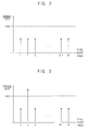
- FIG. 2 is a graph illustrating ratios of measured current values to corresponding block data when an overcurrent does not occur
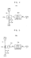
- FIG. 3 is a graph illustrating ratios of measured current values to corresponding block data when an overcurrent occurs.
- the burning protection circuit 100 of a display device includes a plurality of current measuring units 200-1, 200-2,..., and 200-N respectively disposed at a plurality of power supply lines PSL1, PSL2, ... , and PSLN, and a control unit 300 that determines whether to cut off power supply to the display device.
- a plurality of pixels included in the display device are grouped into a plurality of pixel blocks BLOCK1, BLOCK2, ... , and BLOCKN that are respectively supplied with power through the power supply lines PSL1, PSL2, ... , and PSLN, and the current measuring units 200-1, 200-2, ... , and 200-N are respectively disposed at the power supply lines PSL1, PSL2, ... , and PSLN coupled to the pixel blocks BLOCK1, BLOCK2,..., and BLOCKN.
- the power supply lines PSL1, PSL2,..., and PSLN may be flexible printed circuit (FPC) lines for supplying power from an external power supply unit to a display panel.
- FPC flexible printed circuit
- the current measuring units 200-1, 200-2, ... , and 200-N generate a corresponding plurality of measured current values MCV1, MCV2, ... , and MCVN by measuring a corresponding plurality of currents respectively supplied to the pixel blocks BLOCK1, BLOCK2,..., and BLOCKN through the power supply lines PSL1, PSL2,..., and PSLN.
- each of the current measuring units 200-1, 200-2,..., and 200-N include a current sensing device for sensing a current flowing through a corresponding one of the power supply lines PSL1, PSL2, ... , and PSLN.
- the current sensing device may include a Hall device (or Hall sensor), a sense resistor, or the like.
- the power supply lines PSL1, PSL2, ... , and PSLN may be high power supply lines, and the current measuring units 200-1, 200-2, ... , and 200-N may measure a corresponding plurality of currents (high power currents) flowing from the high power supply lines to the pixel blocks BLOCK1, BLOCK2,..., and BLOCKN.
- the power supply lines PSL1, PSL2,..., and PSLN may be low power supply lines
- the current measuring units 200-1, 200-2, ... , and 200-N may measure a corresponding plurality of currents (low power currents) flowing from the pixel blocks BLOCK1, BLOCK2, ... , and BLOCKN to the low power supply lines.
- the current measuring units 200-1, 200-2,..., and 200-N may be disposed at high power supply lines and low power supply lines.
- the control unit 300 receives pixel data DATA for the pixels, and calculates a corresponding plurality of block data for the pixel blocks BLOCK1, BLOCK2, ... , and BLOCKN based on the pixel data DATA.
- each block data may be the sum of the pixel data DATA for the pixels included in the corresponding pixel block.
- each block data may be the average of the pixel data DATA for the pixels included in the corresponding pixel block.
- each block data may be a normalized value of the sum or the average of the pixel data DATA for the pixels included in the corresponding pixel block.
- the control unit 300 further receives the measured current values MCV1, MCV2, ... , and MCVN for the pixel blocks BLOCK1, BLOCK2, ... , and BLOCKN from the current measuring units 200-1, 200-2, ... , and 200-N, and calculates a corresponding plurality of ratios of the measured current values MCV1, MCV2,..., and MCVN to the corresponding block data.
- the control unit 300 determines whether an overcurrent occurs in the display device based on the ratios of the measured current values MCV1, MCV2, ... , and MCVN to the corresponding block data.
- control unit 300 may decide that the overcurrent does not occur if all of the ratios of the measured current values MCV1, MCV2,..., and MCVN to the corresponding block data are less than or equal to a set or predetermined threshold value, and may decide that the overcurrent occurs if at least one of the ratios of the measured current values MCV1, MCV2,..., and MCVN to the corresponding block data exceeds the set or predetermined threshold value.
- the current supplied to each pixel is proportional (e.g., substantially linearly proportional) to the corresponding pixel data DATA for the pixel
- the current supplied to each pixel block is proportional (e.g., substantially linearly proportional) to the corresponding block data for the pixel block.
- the respective ratios of the measured current values MCV1, MCV2, ... , and MCVN to the corresponding block data are substantially the same as each other, and less than the set or predetermined threshold value.
- the current supplied to the pixel block where the crack occurs is drastically increased.
- the ratio of the measured current value MCV2 of the second pixel block to the corresponding block data of the second pixel block is greater than the ratios of other pixel blocks, and exceeds the set or predetermined threshold value TVAL.
- the control unit 300 may decide that, for example, a crack in the display device or a short in the power supply voltage line has occurred, and may cut off the power supplied to the pixel blocks BLOCK1, BLOCK2, ... , and BLOCKN or the display device.
- the control unit 300 may control a power supply unit to cut off the power supply to the display device by applying a power-off signal SOFF to the power supply unit.
- control unit 300 calculates the block data corresponding to one frame, and determines whether the overcurrent occurs based on the ratios of the measured current values MCV1, MCV2, ... , and MCVN to the corresponding block data corresponding to one frame. In other example embodiments, the control unit 300 generates a plurality of average block data by respectively averaging pluralities of individual block data for the pixel blocks BLOCK1, BLOCK2, ...
- BLOCKN corresponding to two or more frames, generates a plurality of average measured current values by respectively averaging pluralities of individual measured current values from the current measuring units 200-1, 200-2,..., and 200-N during the two or more frames, and determines that the overcurrent occurs based on a plurality of average ratios of the average measured current values to the corresponding average block data.
- control unit 300 is implemented with a microcontroller, a field programmable gate array (FPGA), an application specific integrated circuit (ASIC), or the like. In other example embodiments, at least a portion of the control unit 300 is included in a timing controller of the display device.
- FPGA field programmable gate array
- ASIC application specific integrated circuit
- a comparable burning protection circuit determines whether an overcurrent occurs by measuring a current supplied to a display panel during a non-emission period of the display device. Thus, when a display device is driven without a non-emission period, for example when the display device is driven with a progressive emission digital driving method, the comparable burning protection circuit cannot detect the overcurrent.
- the burning protection circuit 100 of the display device determines whether the overcurrent occurs based on the ratios of the measured current values MCV1, MCV2,..., and MCVN to the corresponding block data.
- the burning protection circuit 100 detects the overcurrent and protects the display device from burning.
- FIG. 4 is a diagram illustrating an example current measuring unit 200a included in a burning protection circuit in accordance with example embodiments.
- the current measuring unit 200a includes a Hall device 210a (such as a Hall sensor) as a current sensing device that senses a current flowing through a power supply line PSL, and a converter 250a.
- the Hall device 210a generates a sense voltage VS corresponding to an intensity of a magnetic field generated by a current flowing through the power supply line PSL.
- the power supply line PSL is a high power supply line
- the Hall device 210a generates the sense voltage VS corresponding to a current IELVDD flowing from the high power supply line to a pixel block.
- the power supply line PSL is a low power supply line
- the Hall device 210a generates the sense voltage VS corresponding to a current IELVSS flowing from the pixel block to the low power supply line.
- the converter 250a converts the sense voltage VS generated by the Hall device 210a into a measured current value MCV, and provides the measured current value MCV to a control unit.
- the control unit receives the measured current value MCV that is a measured value of the current IELVDD flowing from the high power supply line to the pixel block or of the current IELVSS flowing from the pixel block to the low power supply line.
- the converter 250a is an analog-to-digital converter 250a that converts the analog sense voltage VS output from the Hall device 210a into a digital measured current value MCV.
- the analog-to-digital converter 250a may be included in the current measuring unit 200a, or may be shared by two or more current measuring units 200a.
- the converter 250a may be implemented with a microcontroller, a voltage-to-frequency (VF) converter, or the like.
- the converter 250a may be located inside the control unit.
- the current measuring unit 200a generates the measured current value MCV by sampling the current supplied to the pixel block at least once during a set or predetermined time period.
- the measured current value MCV may be a sampled value generated by sampling the current once during the set or predetermined time period, or may be the sum or the average of sampled values (e.g., a plurality of individual measured current values) generated by sampling the current two or more times (e.g., a plurality of individual currents) during the set or predetermined time period.
- the current measuring unit 200a further includes an amplifier between the Hall device 210a and the converter 250a.
- the amplifier amplifies the sense voltage VS generated by the Hall device 210a.
- FIG. 5 is a diagram illustrating another example current measuring unit 200b included in a burning protection circuit in accordance with example embodiments.
- the current measuring unit 200b includes a sense resistor 210b as a current sensing device that senses a current flowing through a power supply line PSL, an amplifier 230b, and a converter 250b.
- the sense resistor 210b is disposed at the power supply line PSL, and generates a sense voltage VS corresponding to a current flowing through the power supply line PSL.
- the sense resistor 210b has a low resistance such that a voltage or a current supplied to a pixel block through the power supply line PSL is not substantially affected by the sense resistor 210b.
- the power supply line PSL is a high power supply line, and the sense resistor 210b generates the sense voltage VS corresponding to a current IELVDD flowing from the high power supply line to the pixel block.
- the power supply line PSL is a low power supply line, and the sense resistor 210b generates the sense voltage VS corresponding to a current IELVSS flowing from the pixel block to the low power supply line.
- the amplifier 230b generates an amplified sense voltage AVS by amplifying the sense voltage VS generated by the sense resistor 210b.
- the amplifier 230b may be a differential amplifier as illustrated in FIG. 5 .
- the amplifier 230b may be a single ended amplifier.
- FIG. 5 illustrates an example where the current measuring unit 200b includes the amplifier 230b, in some example embodiments, each current measuring unit 200b may be implemented without the amplifier 230b.
- the converter 250b converts the amplified sense voltage AVS output from the amplifier 230b into a measured current value MCV, and provides the measured current value MCV to a control unit.
- the control unit receives the measured current value MCV that is a measured value of the current IELVDD flowing from the high power supply line to the pixel block or the current IELVSS flowing from the pixel block to the low power supply line.
- the converter 250b is an analog-to-digital converter 250b that converts the analog amplified sense voltage AVS output from the amplifier 230b into a digital measured current value MCV.
- the analog-to-digital converter 250b may be included in the current measuring unit 200b, or may be shared by two or more current measuring units 200b.
- the converter 250b may be implemented with a microcontroller, a voltage-to-frequency (VF) converter, or the like.
- the converter 250b may be located inside the control unit.
- the current measuring unit 200b generates the measured current value MCV by sampling the current supplied to the pixel block at least once during a set or predetermined time period.
- the measured current value MCV may be a sampled value generated by sampling the current once during the set or predetermined time period, or may be the sum or the average of sampled values (e.g., a plurality of individual measured current values) generated by sampling the current two or more times (e.g., a plurality of individual currents) during the set or predetermined time period.
- FIG. 6 is a diagram illustrating an example control unit 300a included in a burning protection circuit in accordance with example embodiments.
- control unit 300a of a burning protection circuit includes a block data calculating unit 310a and an overcurrent determining unit 350a.
- the block data calculating unit 310a receives pixel data DATA for a plurality of pixels included in a display device from a host device, and generates (e.g., calculates) a plurality of block data BD1, BD2, ... , and BDN for a corresponding plurality of pixel blocks BLOCK1, BLOCK2, ... , and BLOCKN based on the pixel data DATA for the pixels.
- each of the block data BD1, BD2,..., and BDN is the sum of the pixel data DATA for the pixels included in a corresponding one of the pixel blocks BLOCK1, BLOCK2, ... , and BLOCKN.
- each of the block data BD1, BD2,..., and BDN is the average of the pixel data DATA for the pixels included in the corresponding one of the pixel blocks BLOCK1, BLOCK2,..., and BLOCKN.
- each of the block data BD1, BD2, ... , and BDN is a normalized value of the sum or the average of the pixel data DATA for the pixels included in the corresponding one of the pixel blocks BLOCK1, BLOCK2,..., and BLOCKN.
- the overcurrent determining unit 350a respectively receives a plurality of measured current values MCV1, MCV2, ... , and MCVN for the pixel blocks BLOCK1, BLOCK2, ... , and BLOCKN from a corresponding plurality of current measuring units.
- the measured current values MCV1, MCV2,..., and MCVN are measured values of a plurality of currents respectively supplied to the pixel blocks BLOCK1, BLOCK2,..., and BLOCKN.
- Each of the measured current values MCV1, MCV2, ... , and MCVN are generated by sampling a current supplied to a corresponding one of the pixel blocks BLOCK1, BLOCK2,..., and BLOCKN at least once during a set or predetermined time period.
- the set or predetermined time period corresponds to at least one frame.
- the overcurrent determining unit 350a further receives the block data BD1, BD2, ... , and BDN for the corresponding plurality of pixel blocks BLOCK1,
- BLOCK2, ... , and BLOCKN from the block data calculating unit 310a, and calculates a plurality of ratios of the measured current values MCV1, MCV2, ... , and MCVN to the corresponding block data BD1, BD2, ... , and BDN. Since a current supplied to each pixel is proportional (e.g., substantially linearly proportional) to a corresponding pixel data DATA for the pixel, a current supplied to each pixel block is proportional (e.g., substantially linearly proportional) to a corresponding block data for the pixel block.
- the respective ratios of the measured current values MCV1, MCV2, ... , and MCVN to the corresponding block data BD1, BD2, ... , and BDN are substantially the same as each other.
- the overcurrent determining unit 350a determines whether an overcurrent occurs by comparing the ratios of the measured current values MCV1, MCV2, ... , and MCVN to the corresponding block data BD1, BD2, ... , and BDN with a set or predetermined threshold value. For example, the overcurrent determining unit 350a may decide that the overcurrent does not occur if all of the ratios of the measured current values MCV1, MCV2, ... , and MCVN to the corresponding block data BD1, BD2, ... , and BDN are less than or equal to the set or predetermined threshold value, and may decide that the overcurrent occurs if at least one of the ratios of the measured current values MCV1, MCV2, ...
- the overcurrent determining unit 350a applies a power-off signal SOFF to a power supply unit to cut off the power supply to the display device.
- the burning protection circuit including the control unit 300a performs the overcurrent determination operation continuously (for example, at each and every frame) or non-continuously (for example, once during a set or predetermined number of frames)
- control unit 300a is implemented with a microcontroller, a field programmable gate array (FPGA), an application specific integrated circuit (ASIC), or the like.
- FPGA field programmable gate array
- ASIC application specific integrated circuit
- at least a portion of the control unit 300a is included in a timing controller of the display device.
- the block data calculating unit 310a may be implemented inside the timing controller.
- the burning protection circuit including the control unit 300a determines whether the overcurrent occurs based on the ratios of the measured current values MCV1, MCV2,..., and MCVN to the corresponding block data BD1, BD2, ... , and BDN, and thus accurately detects the overcurrent even if the display device is driven without a non-emission period.
- FIG. 7 is a diagram illustrating another example control unit 300b included in a burning protection circuit in accordance with example embodiments.
- the control unit 300b of a burning protection circuit includes a block data calculating unit 310b, an average current calculating unit 330b, and an overcurrent determining unit 350b.
- the block data calculating unit 310b receives pixel data DATA for a plurality of pixels included in a display device from a host device, and calculates a plurality of block data for a corresponding plurality of pixel blocks BLOCK1, BLOCK2,..., and BLOCKN based on the pixel data DATA for the pixels.
- the block data calculating unit 310b calculates the block data at each frame during a set or predetermined time period.
- the block data calculating unit 310b generates a plurality of average block data ABD1, ABD2,..., and ABDN by respectively averaging a plurality of individual block data for each of the pixel blocks BLOCK1, BLOCK2,..., and BLOCKN during the set or predetermined time period, and provides the average block data ABD1, ABD2,..., and ABDN to the overcurrent determining unit 350b.
- the set or predetermined time period may correspond to one frame, or may correspond to two or more frames.
- the block data calculating unit 310b respectively accumulates the individual block data for each of the pixel blocks BLOCK1, BLOCK2, ... , and BLOCKN during the set or predetermined time period, and provides the overcurrent determining unit 350b with the accumulated block data or average or normalized values of the accumulated block data.
- the average current calculating unit 330b receives a plurality of measured current values MCV1, MCV2, ... , and MCVN for the corresponding pixel blocks BLOCK1, BLOCK2, ... , and BLOCKN from a corresponding plurality of current measuring units during the set or predetermined time period.
- the average current calculating unit 330b generates a plurality of average measured current values AMCV1, AMCV2, ... , and AMCVN by respectively averaging a plurality of individual measured current values for each of the pixel blocks BLOCK1, BLOCK2,..., and BLOCKN during the set or predetermined time period.
- the set or predetermined time period may correspond to one frame, or may correspond to two or more frames.
- the average measured current values AMCV1, AMCV2, ... , and AMCVN may be average values of the corresponding pluralities of individual measured current values that are sampled during one frame, or may be average values of the corresponding pluralities of individual measured current values that are sampled during two or more frames.
- the average current calculating unit 330b respectively accumulates the individual measured current values for each of the pixel blocks BLOCK1, BLOCK2,..., and BLOCKN during the set or predetermined time period, and provides the overcurrent determining unit 350b with the accumulated measured current values or average or normalized values of the measured current values.
- the overcurrent determining unit 350b receives the average block data ABD1, ABD2, ... , and ABDN from the block data calculating unit 310b, receives the average measured current values AMCV1, AMCV2, ... , and AMCVN from the average current calculating unit 330b, and calculates a corresponding plurality of ratios (or average ratios) of the average measured current values AMCV1, AMCV2, ... , and AMCVN to the corresponding average block data ABD1, ABD2, ... , and ABDN.
- the overcurrent determining unit 350b receives the accumulated block data from the block data calculating unit 310b, receives the accumulated measured current values from the average current calculating unit 330b, and calculates a corresponding plurality of ratios of the accumulated measured current values to the corresponding accumulated block data.
- the overcurrent determining unit 350b determines whether an overcurrent occurs by comparing the average ratios of the average measured current values AMCV1, AMCV2, ... , and AMCVN to the corresponding average block data ABD1, ABD2, ... , and ABDN with a set or predetermined threshold value.
- the overcurrent determining unit 350b may decide that the overcurrent does not occur if all of the average ratios of the average measured current values AMCV1, AMCV2, ... , and AMCVN to the corresponding average block data ABD1, ABD2, ... , and ABDN are less than or equal to the set or predetermined threshold value, and may decide that the overcurrent occurs if at least one of the average ratios of the average measured current values AMCV1, AMCV2, ... , and AMCVN to the corresponding average block data ABD1, ABD2,..., and ABDN exceeds the set or predetermined threshold value.
- the overcurrent determining unit 350b applies a power-off signal SOFF to a power supply unit to cut off power supply to the display device.
- the burning protection circuit including the control unit 300b determines whether the overcurrent occurs based on the average ratios of the average measured current values AMCV1, AMCV2, ... , and AMCVN to the corresponding average block data ABD1, ABD2,..., and ABDN, and thus accurately detects the overcurrent even if the display device is driven without the non-emission period.
- the burning protection circuit including the control unit 300b uses the average measured current values AMCV1, AMCV2, ... , and AMCVN that are average values of the corresponding pluralities of individual measured current values during two or more frames, and the corresponding average block data ABD1, ABD2, ... , and ABDN that are average values of the corresponding pluralities of individual block data during two or more frames to determine whether the overcurrent occurs, and thus may more accurately detect the overcurrent.
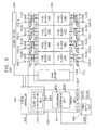
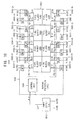
- FIG. 8 is a block diagram illustrating a display device 1000 in accordance with example embodiments.
- the display device 1000 includes a display panel 1400 including a plurality of pixel blocks 1410,1420,1430,1440,1450,1460,1470, and 1480, a power supply unit 1800, and a burning protection circuit 1100.
- the display device 1000 further includes a scan driver 1500, a source driver 1600, a timing controller 1700, or the like.
- the display panel 1400 includes a plurality of pixels that are arranged in a matrix having a plurality of rows and a plurality of columns.
- the pixels are grouped into the pixel blocks 1410, 1420, 1430, 1440, 1450, 1460, 1470, and 1480 that are respectively supplied with power through a corresponding plurality of high power supply lines PSL1, PSL2, PSL3, PSL4, PSL5, PSL6, PSL7, and PSL8, and a plurality (e.g., a corresponding plurality) of low power supply lines (see, e.g., the power lines connecting low power source voltage ELVSS to each of the pixel blocks 1410, 1420, 1430, 1440, 1450, 1460, 1470, and 1480 in FIG. 8 ).
- the high power supply lines PSL1, PSL2, PSL3, PSL4, PSL5, PSL6, PSL7, and PSL8 and the low power supply lines areflexible printed circuit (FPC) lines for supplying power from the power supply unit 1800 to the display panel 1400.
- the display panel 1400 is an organic light emitting display (OLED) panel.
- the display panel 1400 is a liquid crystal display (LCD) panel, a plasma display panel (PDP), or the like.
- the scan driver 1500 and the source driver 1600 are controlled by the timing controller 1700 to drive the display panel 1400.
- the scan driver 1500 turns on or off thin film transistors (TFTs) formed in the display panel 1400.
- the source driver 1600 applies data voltages to the pixels based on data provided from the timing controller 1700.
- the timing controller 1700 receives pixel data DATA for the pixels and controls signals from a host device.
- the control signals may include a vertical synchronization signal (VSYNC), a horizontal synchronization signal (HSYNC), a clock signal (CLK), and a data enable signal (DE).
- VSYNC vertical synchronization signal
- HSELNC horizontal synchronization signal
- CLK clock signal
- DE data enable signal
- the timing controller 1700 Based on the pixel data DATA and the control signals, the timing controller 1700 generates the data provided to the source driver 1600 and control signals provided to the scan driver 1500 and the source driver 1600.
- the power supply unit 1800 respectively supplies power to the pixel blocks 1410, 1420, 1430, 1440, 1450, 1460, 1470, and 1480 through the high power supply lines PSL1, PSL2, PSL3, PSL4, PSL5, PSL6, PSL7, and PSL8 and the low power supply lines.
- the power supply unit 1800 provides a high power supply voltage ELVDD to the pixel blocks 1410, 1420, 1430, 1440, 1450, 1460, 1470, and 1480 through the high power supply lines PSL1, PSL2, PSL3, PSL4, PSL5, PSL6, PSL7, and PSL8, respectively, and provides a low power supply voltage ELVSS to the pixel blocks 1410, 1420, 1430, 1440, 1450, 1460, 1470, and 1480 through the low power supply lines, respectively.
- the burning protection circuit 1100 detects an overcurrent (or an occurrence of the overcurrent), and cuts off the power supplied to the pixel blocks 1410, 1420, 1430, 1440, 1450, 1460, 1470, and 1480 when the overcurrent (or the occurrence of the overcurrent) is detected.
- the burning protection circuit 1100 includes a plurality of current measuring units 1200-1, 1200-2, 1200-3, 1200-4, 1200-5, 1200-6, 1200-7, and 1200-8 (also respectively labeled CMU1, CMU2, CMU3, CMU4, CMU5, CMU6, CMU7, and CMU8), and a control unit 1300.
- the current measuring units 1200-1, 1200-2, 1200-3, 1200-4, 1200-5, 1200-6, 1200-7, and 1200-8 generate a plurality of measured current values MCV1, MCV2, MCV3, MCV4, MCV5, MCV6, MCV7, and MCV8 by measuring a corresponding plurality of currents I1, I2, I3, I4, I5, I6, I7, and I8 supplied to the corresponding pixel blocks 1410, 1420, 1430, 1440, 1450, 1460, 1470, and 1480.
- the current measuring units 1200-1, 1200-2, 1200-3, 1200-4, 1200-5, 1200-6, 1200-7, and 1200-8 are respectively disposed at the high power supply lines PSL1, PSL2, PSL3, PSL4, PSL5, PSL6, PSL7, and PSL8, and the currents I1, 12, I3, I4, 15, 16, I7, and I8 respectively flowing from the high power supply lines PSL1, PSL2, PSL3, PSL4, PSL5, PSL6, PSL7, and PSL8 to the pixel blocks 1410, 1420, 1430, 1440, 1450, 1460, 1470, and 1480 are measured.
- the control unit 1300 determines whether the overcurrent occurs based on the pixel data DATA for the pixels and the measured current values MCV1, MCV2, MCV3, MCV4, MCV5, MCV6, MCV7, and MCV8.
- the control unit 1300 includes a block data calculating unit 1310 that respectively calculates a plurality of block data BD1, BD2,..., BD8 for the corresponding pixel blocks 1410, 1420, 1430, 1440, 1450, 1460, 1470, and 1480 based on the pixel data DATA.
- the block data calculating unit 1310 is located inside the control unit 1300. In other example embodiments, the block data calculating unit 1310 is located outside the control unit 1300.
- the control unit 1300 further includes an overcurrent determining unit 1350 that receives the block data BD1, BD2, ... , BD8 from the block data calculating unit 1310, receives the measured current values MCV1, MCV2, MCV3, MCV4, MCV5, MCV6, MCV7, and MCV8 from the current measuring units 1200-1, 1200-2, 1200-3, 1200-4, 1200-5, 1200-6, 1200-7, and 1200-8, and calculates a plurality of ratios of the measured current values MCV1, MCV2, MCV3, MCV4, MCV5, MCV6, MCV7, and MCV8 to the corresponding block data BD1, BD2, ... , BD8.
- an overcurrent determining unit 1350 that receives the block data BD1, BD2, ... , BD8 from the block data calculating unit 1310, receives the measured current values MCV1, MCV2, MCV3, MCV4, MCV5, MCV6, MCV7, and MCV8 from the current measuring units 1200-1
- the overcurrent determining unit 1350 determines whether the overcurrent occurs based on the ratios of the measured current values MCV1, MCV2, MCV3, MCV4, MCV5, MCV6, MCV7, and MCV8 to the corresponding block data BD1, BD2, ... , BD8.
- the overcurrent determining unit 1350 decides that the overcurrent occurs if at least one of the ratios of the measured current values MCV1, MCV2, MCV3, MCV4, MCV5, MCV6, MCV7, and MCV8 to the corresponding block data BD1, BD2,..., BD8 exceeds a set or predetermined threshold value.
- the overcurrent determining unit 1350 applies a power-off signal SOFF to the power supply unit 1800 to cut off the power supply to the display device 1000. Accordingly, a burn or a fire may be prevented in the display device 1000 even if a crack occurs in the display panel 1400, or a line (e.g., a power supply line) is abnormally shorted.
- the display device 1000 determines whether the overcurrent occurs based on the ratios of the measured current values MCV1, MCV2, MCV3, MCV4, MCV5, MCV6, MCV7, and MCV8 to the corresponding block data BD1, BD2, ... , BD8, thereby accurately detecting the overcurrent and securely protecting the display device 1000 from burning even if the display device 1000 is driven without a non-emission period (e.g., by a PESS method).
- FIG. 9 is a diagram illustrating an example high power supply voltage line included in a display device in accordance with example embodiments
- FIG. 10 is a graph illustrating ratios of measured current values to corresponding block data when an overcurrent occurs in a display device including the high power supply voltage line illustrated in FIG. 9 .
- the display panel includes a display panel 1400a that includes an integrated high power supply voltage line HPSVL having a mesh structure that is shared by a plurality of pixel blocks PB1, PB2, PB3, PB4, PB5, PB6, PB7, and PB8.
- the high power supply voltage line HPSVL supplies respective pixels included in the pixel blocks PB1, PB2, PB3, PB4, PB5, PB6, PB7, and PB8 with a high power supply voltage ELVDD provided from a corresponding plurality of high power supply lines PSL1, PSL2, PSL3, PSL4, PSL5, PSL6, PSL7, and PSL8.
- the high power supply voltage line HPSVL includes a plurality of main power supply voltage lines and a plurality of sub-power supply voltage lines.
- the main power supply voltage lines and the sub-power supply voltage lines may be coupled to each other via a plurality of contacts, or may be integrally formed.
- the high power supply voltage line HPSVL is coupled to the high power supply lines PSL1, PSL2, PSL3, PSL4, PSL5, PSL6, PSL7, and PSL8, and receives the high power supply voltage ELVDD through the high power supply lines PSL1, PSL2, PSL3, PSL4, PSL5, PSL6, PSL7, and PSL8.
- the high power supply voltage line HPSVL is further coupled to all pixels included in the display panel 1400a, and provides the high power supply voltage ELVDD to all the pixels included in the display panel 1400a. That is, the high power supply voltage line HPSVL may be a single or integrated power supply voltage line corresponding to all the pixel blocks PB1, PB2, PB3, PB4, PB5, PB6, PB7, and PB8.
- a plurality of current measuring units 1200-1, 1200-2, 1200-3, 1200-4, 1200-5, 1200-6, 1200-7, and 1200-8 (also respectively labeled CMU1, CMU2, CMU3, CMU4, CMU5, CMU6, CMU7, and CMU8), and a control unit 1300 are respectively disposed at the high power supply lines PSL1, PSL2, PSL3, PSL4, PSL5, PSL6, PSL7, and PSL8, and measure a corresponding plurality of currents I1, 12, I3, 14, I5, I6, I7, and I8 supplied from the high power supply lines PSL1, PSL2, PSL3, PSL4, PSL5, PSL6, PSL7, and PSL8 to the single high power supply voltage line HPSVL.
- the current I2 supplied through the high power supply line PSL2 corresponding to the second pixel block PB2 is greatly increased as illustrated in FIG. 10 .
- a ratio of a measured value of the current I2 to block data for the second pixel block PB2 is higher than a set or predetermined threshold value TVAL, and a burning protection circuit according to example embodiments cut off power supply to a corresponding display device.
- FIG. 11 is a diagram illustrating another example high power supply voltage line included in a display device in accordance with example embodiments
- FIG. 12 is a graph illustrating ratios of measured current values to corresponding block data when an overcurrent occurs in a display device including the high power supply voltage line illustrated in FIG. 11 .
- a display panel 1400b includes a plurality of high power supply voltage lines HPSVL1, HPSVL2, HPSVL3, HPSVL4, HPSVL5, HPSVL6, HPSVL7, and HPSVL8 that supply a corresponding plurality of pixel blocks PB1, PB2, PB3, PB4, PB5, PB6, PB7, and PB8 with a corresponding plurality of high power supply voltages ELVDD1, ELVDD2, ELVDD3, ELVDD4, ELVDD5, ELVDD6, ELVDD7, and ELVDD8 through a corresponding plurality of high power supply lines PSL1, PSL2, PSL3, PSL4, PSL5, PSL6, PSL7, and PSL8.
- each of the high power supply voltage lines HPSVL1, HPSVL2, HPSVL3, HPSVL4, HPSVL5, HPSVL6, HPSVL7, and HPSVL8 include a plurality of main power supply voltage lines and a plurality of sub-power supply voltage lines.
- the main power supply voltage lines and the sub-power supply voltage lines may be coupled to each other via a plurality of contacts, or may be integrally formed.
- the high power supply voltage lines HPSVL1, HPSVL2, HPSVL3, HPSVL4, HPSVL5, HPSVL6, HPSVL7, and HPSVL8 are respectively coupled to the high power supply lines PSL1, PSL2, PSL3, PSL4, PSL5, PSL6, PSL7, and PSL8, and respectively receive the high power supply voltages ELVDD1, ELVDD2, ELVDD3, ELVDD4, ELVDD5, ELVDD6, ELVDD7, and ELVDD8 through the high power supply lines PSL1, PSL2, PSL3, PSL4, PSL5, PSL6, PSL7, and PSL8.
- the high power supply voltages ELVDD1, ELVDD2, ELVDD3, ELVDD4, ELVDD5, ELVDD6, ELVDD7, and ELVDD8 have substantially the same voltage level.
- Each of the high power supply voltage lines HPSVL1, HPSVL2, HPSVL3, HPSVL4, HPSVL5, HPSVL6, HPSVL7, and HPSVL8 are coupled to all pixels included in a corresponding one of the pixel blocks PB1, PB2, PB3, PB4, PB5, PB6, PB7, and PB8, and provide a corresponding one of the high power supply voltages ELVDD1, ELVDD2, ELVDD3, ELVDD4, ELVDD5, ELVDD6, ELVDD7, and ELVDD8 to all the pixels included in the corresponding one of the pixel blocks PB1, PB2, PB3, PB4, PB5, PB6, PB7, and PB8.
- the high power supply voltage lines HPSVL1, HPSVL2, HPSVL3, HPSVL4, HPSVL5, HPSVL6, HPSVL7, and HPSVL8 respectively correspond to the pixel blocks PB1, PB2, PB3, PB4, PB5, PB6, PB7, and PB8.
- a plurality of current measuring units 1200-1, 1200-2, 1200-3, 1200-4, 1200-5, 1200-6, 1200-7, and 1200-8 (also respectively labeled CMU1, CMU2, CMU3, CMU4, CMU5, CMU6, CMU7, and CMU8), and a control unit 1300 are respectively disposed at the high power supply lines PSL1, PSL2, PSL3, PSL4, PSL5, PSL6, PSL7, and PSL8, and measure a corresponding plurality of currents I1, I2, I3, I4, I5, 16, 17, and I8 respectively supplied from the high power supply lines PSL1, PSL2, PSL3, PSL4, PSL5, PSL6, PSL7, and PSL8 to the high power supply voltage lines HPSVL1, HPSVL2, HPSVL3, HPSVL4, HPSVL5, HPSVL6, HPSVL7, and HPSVL8.
- the current supplied from the high power supply line corresponding to the pixel block having the crack may be greatly increased.
- the current I2 supplied through the high power supply line PSL2 corresponding to the second pixel block PB2 may be greatly increased as illustrated in FIG. 12 .
- a ratio of a measured value of the current I2 to block data for the second pixel block PB2 may be higher than a set or predetermined threshold value TVAL, and a burning protection circuit according to example embodiments may cut off power supply to a corresponding display device.
- FIG. 13 is a block diagram illustrating another display device 2000 in accordance with example embodiments
- FIG. 14 is a diagram illustrating an example low power supply voltage line included in a display device in accordance with example embodiments
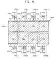
- FIG. 15 is a diagram illustrating another example low power supply voltage line included in a display device in accordance with example embodiments.
- the display device 2000 includes a display panel 2400 including a plurality of pixel blocks 2410, 2420, 2430, 2440, 2450, 2460, 2470, and 2480, a power supply unit 2800, and a burning protection circuit 2100.
- the display device 2000 of FIG. 13 may have substantially the same configuration as the display device 1000 of FIG.
- a plurality of current measuring units 2200-1, 2200-2, 2200-3, 2200-4, 2200-5, 2200-6, 2200-7, and 2200-8 are respectively disposed at a corresponding plurality of low power supply lines PSL1, PSL2, PSL3, PSL4, PSL5, PSL6, PSL7, and PSL8.
- the display panel 2400 includes a plurality of pixels that are arranged in a matrix having a plurality of rows and a plurality of columns.
- the pixels are grouped into the pixel blocks 2410, 2420, 2430, 2440, 2450, 2460, 2470, and 2480 that are respectively supplied with power through a plurality of high power supply lines (see, e.g., the power lines connecting high power source voltage ELVDD to each of the pixel blocks 2410, 2420, 2430, 2440, 2450, 2460, 2470, and 2480 in FIG. 13 ) and a plurality of low power supply lines PSL1, PSL2, PSL3, PSL4, PSL5, PSL6, PSL7, and PSL8.
- a plurality of high power supply lines see, e.g., the power lines connecting high power source voltage ELVDD to each of the pixel blocks 2410, 2420, 2430, 2440, 2450, 2460, 2470, and 2480 in FIG. 13
- the power supply unit 2800 provides a high power supply voltage ELVDD to the pixel blocks 2410, 2420, 2430, 2440, 2450, 2460, 2470, and 2480 through the corresponding high power supply lines, and provides a low power supply voltage ELVSS to the pixel blocks 2410, 2420, 2430, 2440, 2450, 2460, 2470, and 2480 through the corresponding low power supply lines PSL1, PSL2, PSL3, PSL4, PSL5, PSL6, PSL7, and PSL8.
- the burning protection circuit 2100 detects an overcurrent (or an occurrence of the overcurrent), and cuts off the power supply to the display device 2000 when the overcurrent (or the occurrence of the overcurrent) is detected.
- the burning protection circuit 2100 includes the plurality of current measuring units 2200-1, 2200-2, 2200-3, 2200-4, 2200-5, 2200-6, 2200-7, and 2200-8, and a control unit 2300.
- the current measuring units 2200-1, 2200-2, 2200-3, 2200-4, 2200-5, 2200-6, 2200-7, and 2200-8 are respectively disposed at the low power supply lines PSL1, PSL2, PSL3, PSL4, PSL5, PSL6, PSL7, and PSL8, and measure a corresponding plurality of currents I1, 12, I3, 14, 15, 16, I7, and I8 respectively flowing from the pixel blocks 2410, 2420, 2430, 2440, 2450, 2460, 2470, and 2480 to the low power supply lines PSL1, PSL2, PSL3, PSL4, PSL5, PSL6, PSL7, and PSL8.
- the display panel 2400a includes a low power supply voltage line LPSVL that is shared by a plurality of pixel blocks PB1, PB2, PB3, PB4, PB5, PB6, PB7, and PB8.
- the low power supply voltage line LPSVL supplies respective pixels included in the pixel blocks PB1, PB2, PB3, PB4, PB5, PB6, PB7, and PB8 with a low power supply voltage ELVSS provided from the corresponding low power supply lines PSL1, PSL2, PSL3, PSL4, PSL5, PSL6, PSL7, and PSL8.
- the low power supply voltage line LPSVL may be a single or integrated power supply voltage line corresponding to all the pixel blocks PB1, PB2, PB3, PB4, PB5, PB6, PB7, and PB8.
- the low power supply voltage line LPSVL may be a transparent or reflective electrode that covers the entire surface of the display panel 2400a.
- the current measuring units 2200-1, 2200-2, 2200-3, 2200-4, 2200-5, 2200-6, 2200-7, and 2200-8 (also respectively labeled CMU1, CMU2, CMU3, CMU4, CMU5, CMU6, CMU7, and CMU8) measure the corresponding currents I1, I2, I3, I4, I5, I6, I7, and I8 flowing from the integrated low power supply voltage line LPSVL to the low power supply lines PSL1, PSL2, PSL3, PSL4, PSL5, PSL6, PSL7, and PSL8, respectively.
- the display panel 2400b includes a plurality of low power supply voltage lines LPSVL1, LPSVL2, LPSVL3, LPSVL4, LPSVL5, LPSVL6, LPSVL7, and LPSVL8 that supply a corresponding plurality of pixel blocks PB1, PB2, PB3, PB4, PB5, PB6, PB7, and PB8 with a corresponding plurality of low power supply voltages ELVSS1, ELVSS2, ELVSS3, ELVSS4, ELVSS5, ELVSS6, ELVSS7, and ELVSS8 through a plurality of low power supply lines PSL1, PSL2, PSL3, PSL4, PSL5, PSL6, PSL7, and PSL8, respectively.
- LPSVL1, LPSVL2, LPSVL3, LPSVL4, LPSVL5, LPSVL6, LPSVL7, and LPSVL8 that supply a corresponding plurality of pixel blocks PB1, PB2, PB3, PB4, PB5,
- the low power supply voltage lines LPSVL1, LPSVL2, LPSVL3, LPSVL4, LPSVL5, LPSVL6, LPSVL7, and LPSVL8 respectively correspond to the pixel blocks PB1, PB2, PB3, PB4, PB5, PB6, PB7, and PB8.
- each of the low power supply voltage lines LPSVL1, LPSVL2, LPSVL3, LPSVL4, LPSVL5, LPSVL6, LPSVL7, and LPSVL8 may be a transparent or reflective electrode that covers the entire surface of a corresponding one of the pixel blocks PB1, PB2, PB3, PB4, PB5, PB6, PB7, and PB8.
- the current measuring units 2200-1, 2200-2, 2200-3, 2200-4, 2200-5, 2200-6, 2200-7, and 2200-8 (also respectively labeled CMU1, CMU2, CMU3, CMU4, CMU5, CMU6, CMU7, and CMU8) measure the corresponding currents I1, 12, I3, I4, 15, I6, I7, and I8 flowing from the low power supply voltage lines LPSVL1, LPSVL2, LPSVL3, LPSVL4, LPSVL5, LPSVL6, LPSVL7, and LPSVL8 to the low power supply lines PSL1, PSL2, PSL3, PSL4, PSL5, PSL6, PSL7, and PSL8, respectively.
- the control unit 2300 calculates a plurality of block data for the corresponding pixel blocks 2410, 2420, 2430, 2440, 2450, 2460, 2470, and 2480 based on pixel data DATA for the pixels, calculates a plurality of ratios of the measured current values to the corresponding block data, and determines whether an overcurrent occurs based on the ratios of the measured current values to the corresponding block data.
- the control unit 2300 applies a power-off signal SOFF to the power supply unit 2800 to cut off the power supply to the display device 2000. Accordingly, a burn or a fire may be prevented in the display device 2000 even if a crack occurs in the display panel 2400, or a line (e.g., a power supply line) is abnormally shorted.
- the display device 2000 determines whether the overcurrent occurs based on the ratios of the measured current values to the corresponding block data, thereby accurately detecting the overcurrent and securely protecting the display device 2000 from burning even if the display device 2000 is driven without a non-emission period (e.g., by a PESS method).
- FIG. 16 is a block diagram illustrating yet another display device 3000 in accordance with example embodiments.
- the display device 3000 includes a display panel 3400 including a plurality of pixel blocks 3410, 3420, 3430, 3440, 3450, 3460, 3470, and 3480, a power supply unit 3800, and a burning protection circuit 3100.
- the display device 3000 of FIG. 16 may have substantially the same configuration as the display device 1000 of FIG.
- a plurality of first current measuring units 3200-11, 3200-12, 3200-13, 3200-14, 3200-15, 3200-16, 3200-17, and 3200-18 (also respectively labeled CMU11, CMU12, CMU13, CMU14, CMU15, CMU16, CMU17, and CMU18) are respectively disposed at a plurality of high power supply lines PSL11, PSL12, PSL13, PSL14, PSL15, PSL16, PSL17, and PSL18, and a plurality of second current measuring units 3200-21, 3200-22, 3200-23, 3200-24, 3200-25, 3200-26, 3200-27, and 3200-28 (also respectively labeled CMU21, CMU22, CMU23, CMU24, CMU25, CMU26, CMU27, and CMU28) are respectively disposed at a plurality of low power supply lines PSL21, PSL22, PSL23, PSL24, PSL25, PSL26,
- the display panel 3400 includes a plurality of pixels that are arranged in a matrix having a plurality of rows and a plurality of columns.
- the pixels are grouped into the pixel blocks 3410, 3420, 3430, 3440, 3450, 3460, 3470, and 3480 that are respectively supplied with power through the high power supply lines PSL11, PSL12, PSL13, PSL14, PSL15, PSL16, PSL17, and PSL18 and the low power supply lines PSL21, PSL22, PSL23, PSL24, PSL25, PSL26, PSL27, and PSL28.
- the power supply unit 3800 provides a high power supply voltage ELVDD to the pixel blocks 3410, 3420, 3430, 3440, 3450, 3460, 3470, and 3480 through the high power supply lines PSL11, PSL12, PSL13, PSL14, PSL15, PSL16, PSL17, and PSL18, respectively, and provides a low power supply voltage ELVSS to the pixel blocks 3410, 3420, 3430, 3440, 3450, 3460, 3470, and 3480 through the low power supply lines PSL21, PSL22, PSL23, PSL24, PSL25, PSL26, PSL27, and PSL28, respectively.
- the burning protection circuit 3100 detects an overcurrent (or an occurrence of the overcurrent), and cuts off the power supply to the display device 3000 when the overcurrent (or the occurrence of the overcurrent) is detected.
- the burning protection circuit 3100 includes the first current measuring units 3200-11, 3200-12, 3200-13, 3200-14, 3200-15, 3200-16, 3200-17, and 3200-18 respectively coupled to the high power supply lines PSL11, PSL12, PSL13, PSL14, PSL15, PSL16, PSL17, and PSL18, the second current measuring units 3200-21, 3200-22, 3200-23, 3200-24, 3200-25, 3200-26, 3200-27, and 3200-28 respectively coupled to the low power supply lines PSL21, PSL22, PSL23, PSL24, PSL25, PSL26, PSL27, and PSL28, and a control unit 3300.
- the first current measuring units 3200-11, 3200-12, 3200-13, 3200-14, 3200-15, 3200-16, 3200-17, and 3200-18 are respectively disposed at the high power supply lines PSL11, PSL12, PSL13, PSL14, PSL15, PSL16, PSL17, and PSL18, and measure a corresponding plurality of first currents I11, I12, 113, I14, I15, 116, 117, and I18 (e.g., high power currents) respectively flowing from the high power supply lines PSL11, PSL12, PSL13, PSL14, PSL15, PSL16, PSL17, and PSL18 to the corresponding pixel blocks 3410, 3420, 3430, 3440, 3450, 3460, 3470, and 3480.
- the second current measuring units 3200-21, 3200-22, 3200-23, 3200-24, 3200-25, 3200-26, 3200-27, and 3200-28 are respectively disposed at the low power supply lines PSL21, PSL22, PSL23, PSL24, PSL25, PSL26, PSL27, and PSL28, and measure a corresponding plurality of second currents I21, I22, I23, I24, I25, I26, I27, and I28 (e.g., low power currents) respectively flowing from the pixel blocks 3410, 3420, 3430, 3440, 3450, 3460, 3470, and 3480 to the corresponding low power supply lines PSL21, PSL22, PSL23, PSL24, PSL25, PSL26, PSL27, and PSL28.
- second currents I21, I22, I23, I24, I25, I26, I27, and I28 e.g., low power currents
- the control unit 3300 calculates a plurality of block data for the corresponding pixel blocks 3410, 3420, 3430, 3440, 3450, 3460, 3470, and 3480 based on pixel data DATA for the pixels, calculates a plurality of first ratios of measured values of the first currents I11, I12, 113, 114, 115, I16, I17, and 118 to the corresponding block data, calculates a plurality of second ratios of measured values of the second currents I21, I22, I23, I24, I25, I26, I27, and I28 to the corresponding block data, and determines whether an overcurrent occurs based on the first ratios and the second ratios.
- the control unit 3300 applies a power-off signal SOFF to the power supply unit 3800 to cut off the power supply to the display device 3000. Accordingly, a burn or a fire may be prevented in the display device 3000 even if a crack occurs in the display panel 3400, or a line is abnormally shorted.
- the display device 3000 determines whether the overcurrent occurs based on the ratios of the measured current values to the corresponding block data, thereby accurately detecting the overcurrent and securely protecting the display device 3000 from burning even if the display device 3000 is driven without a non-emission period (e.g., by a PESS method).
- FIG. 17 is a flow chart illustrating an example method of protecting a display device from burning in accordance with example embodiments.
- a burning protection circuit calculates a corresponding plurality of block data for the pixel blocks based on pixel data for a plurality of pixels (S410).
- each block data may be the sum, the average, or a normalized value of the pixel data for the pixels included in a corresponding pixel block.
- the burning protection circuit generates a plurality of measured current values by measuring a corresponding plurality of currents respectively supplied to the pixel blocks through the power supply lines (S430). For example, the burning protection circuit measures a plurality of first currents flowing from a corresponding plurality of high power supply lines to the corresponding pixel blocks, a plurality of second currents flowing from the corresponding pixel blocks to a corresponding plurality of low power supply lines, or both of the first currents and the second currents.
- the burning protection circuit calculates a plurality of ratios of the measured current values to the corresponding block data, and determines whether an overcurrent occurs based on the ratios of the measured current values to the corresponding block data (S450). In some example embodiments, the burning protection circuit decides that the overcurrent occurs if at least one of the ratios of the measured current values to the corresponding block data exceeds a set or predetermined threshold value. When the occurrence of the overcurrent is detected, the burning protection circuit cuts off the power supplied to the pixel blocks or the display device.
- the overcurrent is detected based on the ratios of the measured current values to the corresponding block data, and thus, even if the display device is driven without the non-emission period, the overcurrent may be accurately detected.
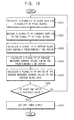
- FIG. 18 is a flow chart illustrating another example method of protecting a display device from burning in accordance with example embodiments.
- a burning protection circuit calculates a corresponding plurality of block data for the pixel blocks based on pixel data for a plurality of pixels (S510).
- the burning protection circuit generates a plurality of measured current values by measuring a corresponding plurality of currents respectively supplied to the pixel blocks through the power supply lines (S520).
- the burning protection circuit generates a plurality of average block data by respectively averaging pluralities of corresponding individual block data during a set or predetermined time period (S530), generates a corresponding plurality of average measured current values by respectively averaging pluralities of individual measured current values for the pixel blocks during the set or predetermined time period (S540), and calculates a corresponding plurality of average ratios of the average measured current values to the corresponding average block data (S550).
- the set or predetermined time period corresponds to one frame, or two or more frames.
- the burning protection circuit determines whether an overcurrent occurs by comparing the respective average ratios of the average measured current values to the corresponding average block data with a set or predetermined threshold value (S560). For example, the burning protection circuit may decide that the overcurrent does not occur if all the average ratios of the average measured current values to the corresponding average block data are less than or equal to a set or predetermined threshold value (S560: NO), and may decide that the overcurrent occurs if at least one of the average ratios of the average measured current values to the corresponding average block data exceeds the set or predetermined threshold value (S560: YES).
- the burning protection circuit cuts off the power supplied to the pixel blocks or the display device to protect the display device from burning (S570).
- FIG. 19 is a block diagram illustrating an electronic device 5000 including a display device 5040 in accordance with example embodiments.
- the electronic device 5000 includes a processor 5010 and the display device 5040.
- the electronic device 5000 further includes a memory device 5020, an input/output device 5030, a modem 5050, and a power supply 5060.
- the processor 5010 performs specific calculations or tasks.
- the processor 5010 may be a system-on-chip (SOC), an application processor, a media processor, a microprocessor, a central process unit (CPU), a digital signal processor, or the like.
- the processor 5010 may be coupled to the memory device 5020 via an address bus, a control bus, and/or a data bus.
- the memory device 5020 may be implemented by a dynamic random access memory (DRAM), a mobile DRAM, a static random access memory (SRAM), a phase change random access memory (PRAM), a resistance random access memory (RRAM), a nano floating gate memory (NFGM), a polymer random access memory (PoRAM), a magnetic random access memory (MRAM), a ferroelectric random access memory (FRAM), etc.
- DRAM dynamic random access memory
- SRAM static random access memory
- PRAM phase change random access memory
- RRAM resistance random access memory
- NFGM nano floating gate memory
- PoRAM polymer random access memory
- MRAM magnetic random access memory
- FRAM ferroelectric random access memory
- the processor 5010 may be coupled to an extension bus, such as a peripheral component interconnect (PCI) bus.
- the processor 5010 may control the input/output device 5030 including an input device, such as a keyboard, a mouse, a keypad, etc., and an output device, such as a printer, a speaker, etc., via the extension bus.
- the processor 5010 may be further coupled to the display device 5040.
- the display device 5040 accurately determines whether an overcurrent occurs based on a plurality of ratios of a plurality of measured current values to a corresponding plurality of block data, and thus protects the electronic device 5000 from burning.
- the processor 5010 may control a storage device, such as a solid state drive, a hard disk drive, a CD-ROM, etc., via the extension bus.
- the modem 5050 may perform wired or wireless communications with an external device.
- the power supply 5060 may supply power to the electronic device 5000.
- the electronic device 5000 may further include an application chipset, a camera image processor (CIS), etc.
- the electronic device 5000 may be any electronic device including the display device 5040, such as a digital television (TV), a 3D TV, a personal computer (PC), a home appliance, a laptop computer, a tablet computer, a cellular phone, a smart phone, a personal digital assistant (PDA), a portable multimedia player (PMP), a digital camera, a music player, a portable game console, a navigation device, etc.
- the display device 5040 such as a digital television (TV), a 3D TV, a personal computer (PC), a home appliance, a laptop computer, a tablet computer, a cellular phone, a smart phone, a personal digital assistant (PDA), a portable multimedia player (PMP), a digital camera, a music player, a portable game console, a navigation device, etc.
Landscapes
- Engineering & Computer Science (AREA)
- Theoretical Computer Science (AREA)
- Physics & Mathematics (AREA)
- General Physics & Mathematics (AREA)
- Computer Hardware Design (AREA)
- General Engineering & Computer Science (AREA)
- Control Of El Displays (AREA)
- Control Of Indicators Other Than Cathode Ray Tubes (AREA)
Abstract
Description
- The present invention relates to a burning protein circuit of a display device, and methods of protecting display devices from burning.
- Recently, various flat panel display devices having reduced weight and volume have been developed. Flat panel display devices include liquid crystal display (LCD) devices, field emission display (FED) devices, plasma display panels (PDPs), organic light emitting display devices, etc. Flat panel display devices may use relatively high currents compared to other electronic devices. Accordingly, when cracks occur in display panels, or power supply voltage lines are abnormally shorted, the flat panel display devices may be vulnerable to burning or catching fire caused by overcurrents.
- The present invention provides for a burning protection circuit of a display device capable of reducing or preventing burning of the display device, and a method of protecting a display device from burning.
- According to the present invention, a burning protection circuit of a display device is provided. The display device includes a plurality of pixel blocks. Each of the pixel blocks includes a plurality of pixels. The pixel blocks are respectively supplied with power through a plurality of power supply lines. The burning protection circuit includes: a plurality of current measuring units configured to respectively generate a plurality of measured current values by respectively measuring a plurality of currents respectively supplied to the pixel blocks through the power supply lines; and a control unit configured to respectively generate a plurality of block data for the pixel blocks based on pixel data for the pixels of corresponding ones of the pixel blocks, and determine whether an overcurrent occurs based on a plurality of ratios of the measured current values to corresponding ones of the block data.
- The control unit may be further configured to determine that the overcurrent occurs when at least one of the ratios exceeds a threshold value.
- The control unit may be further configured to cut off the power supplied to the pixel blocks when the control unit determines that the overcurrent occurs.
- Each of the current measuring units may be further configured to generate a plurality of individual measured current values by measuring a plurality of individual currents supplied to a corresponding one of the pixel blocks through a corresponding one of the power supply lines during a time period. The control unit may be further configured to generate a plurality of individual block data for each pixel block of the pixel blocks based on the pixel data for the pixels of the pixel block during the time period, generate a plurality of average block data by respectively averaging the individual block data for the pixel blocks, generate a plurality of average measured current values by respectively averaging the individual measured current values for the pixel blocks, and determine whether the overcurrent occurs based on a plurality of average ratios of the average measured current values to corresponding ones of the average block data.
- The time period may correspond to one frame.
- Each of the current measuring units may include: a current sensing device configured to sense a corresponding one of the currents flowing through a corresponding one of the power supply lines, and generate a voltage corresponding to the corresponding one of the currents; and a converter configured to convert the voltage generated by the current sensing device into a corresponding one of the measured current values.
- The current sensing device may include a Hall device or a sense resistor.
- The control unit may include: a block data calculating unit configured to respectively generate the block data for the pixel blocks based on the pixel data for the pixels of corresponding ones of the pixel blocks; and an overcurrent determining unit configured to receive the measured current values from the current measuring units, receive the block data from the block data calculating unit; generate the ratios; and determine whether the overcurrent occurs by comparing each of the ratios with a threshold value.
- The control unit may include: a block data calculating unit configured to generate a plurality of individual block data for each pixel block of the pixel blocks based on the pixel data for the pixels of the pixel block during a time period, and generate a plurality of average block data by respectively averaging the individual block data for the pixel blocks; an average current calculating unit configured to receive a plurality of individual measured current values for the time period for each of the pixel blocks from corresponding ones of the current measuring units, and generate a plurality of average measured current values by respectively averaging the individual measured current values for the pixel blocks; and an overcurrent determining unit configured to receive the average measured current values from the average current calculating unit, receive the average block data from the block data calculating unit, generate a plurality of average ratios of the average measured current values to corresponding ones of the average block data, and determine whether the overcurrent occurs by comparing each of the average ratios with a threshold value.
- The power supply lines may include a corresponding plurality of high power supply lines and a corresponding plurality of low power supply lines. The current measuring units may be further configured to respectively measure the currents respectively supplied to the pixel blocks through the high power supply lines.
- The power supply lines may include a corresponding plurality of high power supply lines and a corresponding plurality of low power supply lines. The current measuring units may be further configured to respectively measure the currents respectively supplied to the pixel blocks through the low power supply lines.
- The power supply lines may include a corresponding plurality of high power supply lines and a corresponding plurality of low power supply lines. The currents may include a corresponding plurality of high power currents and a corresponding plurality of low power currents. The current measuring units may be further configured to respectively measure the high power currents respectively supplied to the pixel blocks through the high power supply lines and to respectively measure the low power currents respectively supplied to the pixel blocks through the low power supply lines.
- According to another embodiment of the present invention, a display device is provided. The display device includes: a display panel including a plurality of pixel blocks, each of the pixel blocks including a plurality of pixels; a power supply unit configured to supply power to the pixel blocks through a corresponding plurality of power supply lines; and a burning protection circuit. The burning protection circuit is configured to generate a plurality of block data for the pixel blocks based on pixel data for the pixels of corresponding ones of the pixels, generate a plurality of measured current values by respectively measuring a plurality of currents respectively supplied to the pixel blocks through the power supply lines, and determine whether an overcurrent occurs based on a plurality of ratios of the measured current values to corresponding ones of the block data.
- The burning protection circuit may be further configured to determine that the overcurrent occurs when at least one of the ratios exceeds a threshold value.
- The burning protection circuit may be further configured to control the power supply unit to cut off the power supplied to the pixel blocks when the burning protection circuit determines that the overcurrent occurs.
- The display panel may include a power supply voltage line coupled to the power supply lines and corresponding to all of the pixel blocks. The burning protection circuit may include a plurality of current measuring units configured to respectively measure the currents supplied to the pixel blocks through the power supply voltage line from the power supply lines.
- The display panel may include a plurality of power supply voltage lines respectively coupled to the power supply lines and respectively corresponding to the pixel blocks. The burning protection circuit may include a plurality of current measuring units configured to respectively measure the currents respectively supplied to the pixel blocks through the power supply voltage lines from the power supply lines.
- According to yet another embodiment of the present invention, a method of protecting a display device from burning is provided. The display device includes a plurality of pixel blocks. Each of the pixel blocks includes a plurality of pixels. The pixel blocks are respectively supplied with power through a plurality of power supply lines. The method includes respectively generating a plurality of block data for the pixel blocks based on pixel data for the pixels of corresponding ones of the pixel blocks, generating a plurality of measured current values by respectively measuring a plurality of currents respectively supplied to the pixel blocks through the power supply lines, and determining whether an overcurrent occurs based on a plurality of ratios of the measured current values to corresponding ones of the block data.
- The determining of whether the overcurrent occurs may include determining that the overcurrent occurs when at least one of the ratios exceeds a threshold value.
- The method may further include cutting off the power supplied to the pixel blocks after determining that the overcurrent occurs.
- Embodiments of the present invention may be understood in more detail from the following description taken in conjunction with the accompanying drawings in which:
-
FIG. 1 is a block diagram illustrating a burning protection circuit of a display device in accordance with example embodiments; -
FIG. 2 is a graph illustrating ratios of measured current values to corresponding block data when an overcurrent does not occur; -
FIG. 3 is a graph illustrating ratios of measured current values to corresponding block data when an overcurrent occurs; -
FIG. 4 is a diagram illustrating an example current measuring unit included in a burning protection circuit in accordance with example embodiments; -
FIG. 5 is a diagram illustrating another example current measuring unit included in a burning protection circuit in accordance with example embodiments; -
FIG. 6 is a diagram illustrating an example control unit included in a burning protection circuit in accordance with example embodiments; -
FIG. 7 is a diagram illustrating another example control unit included in a burning protection circuit in accordance with example embodiments; -
FIG. 8 is a block diagram illustrating a display device in accordance with example embodiments; -
FIG. 9 is a diagram illustrating an example high power supply voltage line included in a display device in accordance with example embodiments; -
FIG. 10 is a graph illustrating ratios of measured current values to corresponding block data when an overcurrent occurs in a display device including the high power supply voltage line illustrated inFIG. 9 ; -
FIG. 11 is a diagram illustrating another example high power supply voltage line included in a display device in accordance with example embodiments; -
FIG. 12 is a graph illustrating ratios of measured current values to corresponding block data when an overcurrent occurs in a display device including the high power supply voltage line illustrated inFIG. 11 ; -
FIG. 13 is a block diagram illustrating another display device in accordance with example embodiments; -
FIG. 14 is a diagram illustrating an example low power supply voltage line included in a display device in accordance with example embodiments; -
FIG. 15 is a diagram illustrating another example low power supply voltage line included in a display device in accordance with example embodiments; -
FIG. 16 is a block diagram illustrating yet another display device in accordance with example embodiments; -
FIG. 17 is a flow chart illustrating an example method of protecting a display device from burning in accordance with example embodiments; -
FIG. 18 is a flow chart illustrating another example method of protecting a display device from burning in accordance with example embodiments; and -
FIG. 19 is a block diagram illustrating an electronic device including a display device in accordance with example embodiments. - Example embodiments of the present invention are described more fully hereinafter with reference to the accompanying drawings. Like or similar reference numerals refer to like or similar elements throughout. Herein, the use of the term "may," when describing embodiments of the present invention, refers to "one or more embodiments of the present invention." In addition, the use of alternative language, such as "or," when describing embodiments of the present invention, refers to "one or more embodiments of the present invention" for each corresponding item listed.
-
FIG. 1 is a block diagram illustrating a burningprotection circuit 100 of a display device in accordance with example embodiments,FIG. 2 is a graph illustrating ratios of measured current values to corresponding block data when an overcurrent does not occur, andFIG. 3 is a graph illustrating ratios of measured current values to corresponding block data when an overcurrent occurs. - Referring to
FIG. 1 , the burningprotection circuit 100 of a display device includes a plurality of current measuring units 200-1, 200-2,..., and 200-N respectively disposed at a plurality of power supply lines PSL1, PSL2, ... , and PSLN, and acontrol unit 300 that determines whether to cut off power supply to the display device. - A plurality of pixels included in the display device are grouped into a plurality of pixel blocks BLOCK1, BLOCK2, ... , and BLOCKN that are respectively supplied with power through the power supply lines PSL1, PSL2, ... , and PSLN, and the current measuring units 200-1, 200-2, ... , and 200-N are respectively disposed at the power supply lines PSL1, PSL2, ... , and PSLN coupled to the pixel blocks BLOCK1, BLOCK2,..., and BLOCKN. In some example embodiments, the power supply lines PSL1, PSL2,..., and PSLN may be flexible printed circuit (FPC) lines for supplying power from an external power supply unit to a display panel.
- The current measuring units 200-1, 200-2, ... , and 200-N generate a corresponding plurality of measured current values MCV1, MCV2, ... , and MCVN by measuring a corresponding plurality of currents respectively supplied to the pixel blocks BLOCK1, BLOCK2,..., and BLOCKN through the power supply lines PSL1, PSL2,..., and PSLN. In some example embodiments, each of the current measuring units 200-1, 200-2,..., and 200-N include a current sensing device for sensing a current flowing through a corresponding one of the power supply lines PSL1, PSL2, ... , and PSLN.
- For example, the current sensing device may include a Hall device (or Hall sensor), a sense resistor, or the like. In some example embodiments, the power supply lines PSL1, PSL2, ... , and PSLN may be high power supply lines, and the current measuring units 200-1, 200-2, ... , and 200-N may measure a corresponding plurality of currents (high power currents) flowing from the high power supply lines to the pixel blocks BLOCK1, BLOCK2,..., and BLOCKN.
- In other example embodiments, the power supply lines PSL1, PSL2,..., and PSLN may be low power supply lines, and the current measuring units 200-1, 200-2, ... , and 200-N may measure a corresponding plurality of currents (low power currents) flowing from the pixel blocks BLOCK1, BLOCK2, ... , and BLOCKN to the low power supply lines. In still other example embodiments, the current measuring units 200-1, 200-2,..., and 200-N may be disposed at high power supply lines and low power supply lines.
- The
control unit 300 receives pixel data DATA for the pixels, and calculates a corresponding plurality of block data for the pixel blocks BLOCK1, BLOCK2, ... , and BLOCKN based on the pixel data DATA. In some example embodiments, each block data may be the sum of the pixel data DATA for the pixels included in the corresponding pixel block. In other example embodiments, each block data may be the average of the pixel data DATA for the pixels included in the corresponding pixel block. In still other example embodiments, each block data may be a normalized value of the sum or the average of the pixel data DATA for the pixels included in the corresponding pixel block. - The
control unit 300 further receives the measured current values MCV1, MCV2, ... , and MCVN for the pixel blocks BLOCK1, BLOCK2, ... , and BLOCKN from the current measuring units 200-1, 200-2, ... , and 200-N, and calculates a corresponding plurality of ratios of the measured current values MCV1, MCV2,..., and MCVN to the corresponding block data. Thecontrol unit 300 determines whether an overcurrent occurs in the display device based on the ratios of the measured current values MCV1, MCV2, ... , and MCVN to the corresponding block data. - For example, the
control unit 300 may decide that the overcurrent does not occur if all of the ratios of the measured current values MCV1, MCV2,..., and MCVN to the corresponding block data are less than or equal to a set or predetermined threshold value, and may decide that the overcurrent occurs if at least one of the ratios of the measured current values MCV1, MCV2,..., and MCVN to the corresponding block data exceeds the set or predetermined threshold value. - Since the current supplied to each pixel is proportional (e.g., substantially linearly proportional) to the corresponding pixel data DATA for the pixel, the current supplied to each pixel block is proportional (e.g., substantially linearly proportional) to the corresponding block data for the pixel block. For example, as illustrated in
FIG. 2 , when a crack has not occurred in the display panel, or a line (such as a power supply voltage line) has not been shorted, the respective ratios of the measured current values MCV1, MCV2, ... , and MCVN to the corresponding block data are substantially the same as each other, and less than the set or predetermined threshold value. - However, if a crack occurs in the display panel, or if the power supply voltage line is shorted, the current supplied to the pixel block where the crack occurs is drastically increased. For example, as illustrated in
FIG. 3 , if a crack occurs in a second pixel block, the ratio of the measured current value MCV2 of the second pixel block to the corresponding block data of the second pixel block is greater than the ratios of other pixel blocks, and exceeds the set or predetermined threshold value TVAL. - If at least one of the ratios of the measured current values MCV1, MCV2, ... , and MCVN to the corresponding block data exceeds the set or predetermined threshold value TVAL, the
control unit 300 may decide that, for example, a crack in the display device or a short in the power supply voltage line has occurred, and may cut off the power supplied to the pixel blocks BLOCK1, BLOCK2, ... , and BLOCKN or the display device. For example, thecontrol unit 300 may control a power supply unit to cut off the power supply to the display device by applying a power-off signal SOFF to the power supply unit. - In some example embodiments, the
control unit 300 calculates the block data corresponding to one frame, and determines whether the overcurrent occurs based on the ratios of the measured current values MCV1, MCV2, ... , and MCVN to the corresponding block data corresponding to one frame. In other example embodiments, thecontrol unit 300 generates a plurality of average block data by respectively averaging pluralities of individual block data for the pixel blocks BLOCK1, BLOCK2, ... , and BLOCKN corresponding to two or more frames, generates a plurality of average measured current values by respectively averaging pluralities of individual measured current values from the current measuring units 200-1, 200-2,..., and 200-N during the two or more frames, and determines that the overcurrent occurs based on a plurality of average ratios of the average measured current values to the corresponding average block data. - In some example embodiments, the
control unit 300 is implemented with a microcontroller, a field programmable gate array (FPGA), an application specific integrated circuit (ASIC), or the like. In other example embodiments, at least a portion of thecontrol unit 300 is included in a timing controller of the display device. - A comparable burning protection circuit determines whether an overcurrent occurs by measuring a current supplied to a display panel during a non-emission period of the display device. Thus, when a display device is driven without a non-emission period, for example when the display device is driven with a progressive emission digital driving method, the comparable burning protection circuit cannot detect the overcurrent.
- However, as described above, the burning
protection circuit 100 of the display device according to the present invention determines whether the overcurrent occurs based on the ratios of the measured current values MCV1, MCV2,..., and MCVN to the corresponding block data. Thus, even if the display device is driven without a non-emission period, or for example even if the display device is driven with a progressive emission with simultaneous scan (PESS) method, the burningprotection circuit 100 according to example embodiments detects the overcurrent and protects the display device from burning. -
FIG. 4 is a diagram illustrating an examplecurrent measuring unit 200a included in a burning protection circuit in accordance with example embodiments. - Referring to
FIG. 4 , thecurrent measuring unit 200a includes aHall device 210a (such as a Hall sensor) as a current sensing device that senses a current flowing through a power supply line PSL, and aconverter 250a. TheHall device 210a generates a sense voltage VS corresponding to an intensity of a magnetic field generated by a current flowing through the power supply line PSL. In some example embodiments, the power supply line PSL is a high power supply line, and theHall device 210a generates the sense voltage VS corresponding to a current IELVDD flowing from the high power supply line to a pixel block. In other example embodiments, the power supply line PSL is a low power supply line, and theHall device 210a generates the sense voltage VS corresponding to a current IELVSS flowing from the pixel block to the low power supply line. - The
converter 250a converts the sense voltage VS generated by theHall device 210a into a measured current value MCV, and provides the measured current value MCV to a control unit. Thus, the control unit receives the measured current value MCV that is a measured value of the current IELVDD flowing from the high power supply line to the pixel block or of the current IELVSS flowing from the pixel block to the low power supply line. - In some example embodiments, the
converter 250a is an analog-to-digital converter 250a that converts the analog sense voltage VS output from theHall device 210a into a digital measured current value MCV. The analog-to-digital converter 250a may be included in thecurrent measuring unit 200a, or may be shared by two or morecurrent measuring units 200a. In other example embodiments, theconverter 250a may be implemented with a microcontroller, a voltage-to-frequency (VF) converter, or the like. In some example embodiments, theconverter 250a may be located inside the control unit. - The
current measuring unit 200a generates the measured current value MCV by sampling the current supplied to the pixel block at least once during a set or predetermined time period. For example, the measured current value MCV may be a sampled value generated by sampling the current once during the set or predetermined time period, or may be the sum or the average of sampled values (e.g., a plurality of individual measured current values) generated by sampling the current two or more times (e.g., a plurality of individual currents) during the set or predetermined time period. - In some example embodiments, the
current measuring unit 200a further includes an amplifier between theHall device 210a and theconverter 250a. The amplifier amplifies the sense voltage VS generated by theHall device 210a. -
FIG. 5 is a diagram illustrating another examplecurrent measuring unit 200b included in a burning protection circuit in accordance with example embodiments. - Referring to
FIG. 5 , thecurrent measuring unit 200b includes asense resistor 210b as a current sensing device that senses a current flowing through a power supply line PSL, anamplifier 230b, and aconverter 250b. - The
sense resistor 210b is disposed at the power supply line PSL, and generates a sense voltage VS corresponding to a current flowing through the power supply line PSL. Thesense resistor 210b has a low resistance such that a voltage or a current supplied to a pixel block through the power supply line PSL is not substantially affected by thesense resistor 210b. In some example embodiments, the power supply line PSL is a high power supply line, and thesense resistor 210b generates the sense voltage VS corresponding to a current IELVDD flowing from the high power supply line to the pixel block. In other example embodiments, the power supply line PSL is a low power supply line, and thesense resistor 210b generates the sense voltage VS corresponding to a current IELVSS flowing from the pixel block to the low power supply line. - The
amplifier 230b generates an amplified sense voltage AVS by amplifying the sense voltage VS generated by thesense resistor 210b. In some example embodiments, theamplifier 230b may be a differential amplifier as illustrated inFIG. 5 . In other example embodiments, theamplifier 230b may be a single ended amplifier. AlthoughFIG. 5 illustrates an example where thecurrent measuring unit 200b includes theamplifier 230b, in some example embodiments, eachcurrent measuring unit 200b may be implemented without theamplifier 230b. - The
converter 250b converts the amplified sense voltage AVS output from theamplifier 230b into a measured current value MCV, and provides the measured current value MCV to a control unit. Thus, the control unit receives the measured current value MCV that is a measured value of the current IELVDD flowing from the high power supply line to the pixel block or the current IELVSS flowing from the pixel block to the low power supply line. - In some example embodiments, the
converter 250b is an analog-to-digital converter 250b that converts the analog amplified sense voltage AVS output from theamplifier 230b into a digital measured current value MCV. The analog-to-digital converter 250b may be included in thecurrent measuring unit 200b, or may be shared by two or more current measuringunits 200b. In other example embodiments, theconverter 250b may be implemented with a microcontroller, a voltage-to-frequency (VF) converter, or the like. In some example embodiments, theconverter 250b may be located inside the control unit. - The
current measuring unit 200b generates the measured current value MCV by sampling the current supplied to the pixel block at least once during a set or predetermined time period. For example, the measured current value MCV may be a sampled value generated by sampling the current once during the set or predetermined time period, or may be the sum or the average of sampled values (e.g., a plurality of individual measured current values) generated by sampling the current two or more times (e.g., a plurality of individual currents) during the set or predetermined time period. -
FIG. 6 is a diagram illustrating anexample control unit 300a included in a burning protection circuit in accordance with example embodiments. - Referring to
FIG. 6 , thecontrol unit 300a of a burning protection circuit includes a blockdata calculating unit 310a and anovercurrent determining unit 350a. - The block
data calculating unit 310a receives pixel data DATA for a plurality of pixels included in a display device from a host device, and generates (e.g., calculates) a plurality of block data BD1, BD2, ... , and BDN for a corresponding plurality of pixel blocks BLOCK1, BLOCK2, ... , and BLOCKN based on the pixel data DATA for the pixels. In some example embodiments, each of the block data BD1, BD2,..., and BDN is the sum of the pixel data DATA for the pixels included in a corresponding one of the pixel blocks BLOCK1, BLOCK2, ... , and BLOCKN. In other example embodiments, each of the block data BD1, BD2,..., and BDN is the average of the pixel data DATA for the pixels included in the corresponding one of the pixel blocks BLOCK1, BLOCK2,..., and BLOCKN. In still other example embodiments, each of the block data BD1, BD2, ... , and BDN is a normalized value of the sum or the average of the pixel data DATA for the pixels included in the corresponding one of the pixel blocks BLOCK1, BLOCK2,..., and BLOCKN. - The
overcurrent determining unit 350a respectively receives a plurality of measured current values MCV1, MCV2, ... , and MCVN for the pixel blocks BLOCK1, BLOCK2, ... , and BLOCKN from a corresponding plurality of current measuring units. The measured current values MCV1, MCV2,..., and MCVN are measured values of a plurality of currents respectively supplied to the pixel blocks BLOCK1, BLOCK2,..., and BLOCKN. Each of the measured current values MCV1, MCV2, ... , and MCVN are generated by sampling a current supplied to a corresponding one of the pixel blocks BLOCK1, BLOCK2,..., and BLOCKN at least once during a set or predetermined time period. In some example embodiments, the set or predetermined time period corresponds to at least one frame. - The
overcurrent determining unit 350a further receives the block data BD1, BD2, ... , and BDN for the corresponding plurality of pixel blocks BLOCK1, - BLOCK2, ... , and BLOCKN from the block
data calculating unit 310a, and calculates a plurality of ratios of the measured current values MCV1, MCV2, ... , and MCVN to the corresponding block data BD1, BD2, ... , and BDN. Since a current supplied to each pixel is proportional (e.g., substantially linearly proportional) to a corresponding pixel data DATA for the pixel, a current supplied to each pixel block is proportional (e.g., substantially linearly proportional) to a corresponding block data for the pixel block. Thus, when a crack has not occurred in the display panel, or a line (such as a power supply voltage line) has not been shorted, the respective ratios of the measured current values MCV1, MCV2, ... , and MCVN to the corresponding block data BD1, BD2, ... , and BDN are substantially the same as each other. - The
overcurrent determining unit 350a determines whether an overcurrent occurs by comparing the ratios of the measured current values MCV1, MCV2, ... , and MCVN to the corresponding block data BD1, BD2, ... , and BDN with a set or predetermined threshold value. For example, theovercurrent determining unit 350a may decide that the overcurrent does not occur if all of the ratios of the measured current values MCV1, MCV2, ... , and MCVN to the corresponding block data BD1, BD2, ... , and BDN are less than or equal to the set or predetermined threshold value, and may decide that the overcurrent occurs if at least one of the ratios of the measured current values MCV1, MCV2, ... , and MCVN to the corresponding block data BD1, BD2, ... , and BDN exceeds the set or predetermined threshold value. When it is decided that the overcurrent occurs, theovercurrent determining unit 350a applies a power-off signal SOFF to a power supply unit to cut off the power supply to the display device. - In some example embodiments, while the display device operates, the burning protection circuit including the
control unit 300a performs the overcurrent determination operation continuously (for example, at each and every frame) or non-continuously (for example, once during a set or predetermined number of frames) - In some example embodiments, the
control unit 300a is implemented with a microcontroller, a field programmable gate array (FPGA), an application specific integrated circuit (ASIC), or the like. In other example embodiments, at least a portion of thecontrol unit 300a is included in a timing controller of the display device. For example, the blockdata calculating unit 310a may be implemented inside the timing controller. - As described above, the burning protection circuit including the
control unit 300a according to example embodiments determines whether the overcurrent occurs based on the ratios of the measured current values MCV1, MCV2,..., and MCVN to the corresponding block data BD1, BD2, ... , and BDN, and thus accurately detects the overcurrent even if the display device is driven without a non-emission period. -
FIG. 7 is a diagram illustrating anotherexample control unit 300b included in a burning protection circuit in accordance with example embodiments. - Referring to
FIG. 7 , thecontrol unit 300b of a burning protection circuit includes a blockdata calculating unit 310b, an average current calculatingunit 330b, and anovercurrent determining unit 350b. The blockdata calculating unit 310b receives pixel data DATA for a plurality of pixels included in a display device from a host device, and calculates a plurality of block data for a corresponding plurality of pixel blocks BLOCK1, BLOCK2,..., and BLOCKN based on the pixel data DATA for the pixels. The blockdata calculating unit 310b calculates the block data at each frame during a set or predetermined time period. - In some example embodiments, the block
data calculating unit 310b generates a plurality of average block data ABD1, ABD2,..., and ABDN by respectively averaging a plurality of individual block data for each of the pixel blocks BLOCK1, BLOCK2,..., and BLOCKN during the set or predetermined time period, and provides the average block data ABD1, ABD2,..., and ABDN to theovercurrent determining unit 350b. According to example embodiments, the set or predetermined time period may correspond to one frame, or may correspond to two or more frames. - In other example embodiments, the block
data calculating unit 310b respectively accumulates the individual block data for each of the pixel blocks BLOCK1, BLOCK2, ... , and BLOCKN during the set or predetermined time period, and provides theovercurrent determining unit 350b with the accumulated block data or average or normalized values of the accumulated block data. - The average current calculating
unit 330b receives a plurality of measured current values MCV1, MCV2, ... , and MCVN for the corresponding pixel blocks BLOCK1, BLOCK2, ... , and BLOCKN from a corresponding plurality of current measuring units during the set or predetermined time period. In some example embodiments, the average current calculatingunit 330b generates a plurality of average measured current values AMCV1, AMCV2, ... , and AMCVN by respectively averaging a plurality of individual measured current values for each of the pixel blocks BLOCK1, BLOCK2,..., and BLOCKN during the set or predetermined time period. According to example embodiments, the set or predetermined time period may correspond to one frame, or may correspond to two or more frames. - Thus, the average measured current values AMCV1, AMCV2, ... , and AMCVN may be average values of the corresponding pluralities of individual measured current values that are sampled during one frame, or may be average values of the corresponding pluralities of individual measured current values that are sampled during two or more frames. In other example embodiments, the average current calculating
unit 330b respectively accumulates the individual measured current values for each of the pixel blocks BLOCK1, BLOCK2,..., and BLOCKN during the set or predetermined time period, and provides theovercurrent determining unit 350b with the accumulated measured current values or average or normalized values of the measured current values. - The
overcurrent determining unit 350b receives the average block data ABD1, ABD2, ... , and ABDN from the blockdata calculating unit 310b, receives the average measured current values AMCV1, AMCV2, ... , and AMCVN from the average current calculatingunit 330b, and calculates a corresponding plurality of ratios (or average ratios) of the average measured current values AMCV1, AMCV2, ... , and AMCVN to the corresponding average block data ABD1, ABD2, ... , and ABDN. In other example embodiments, theovercurrent determining unit 350b receives the accumulated block data from the blockdata calculating unit 310b, receives the accumulated measured current values from the average current calculatingunit 330b, and calculates a corresponding plurality of ratios of the accumulated measured current values to the corresponding accumulated block data. - The
overcurrent determining unit 350b determines whether an overcurrent occurs by comparing the average ratios of the average measured current values AMCV1, AMCV2, ... , and AMCVN to the corresponding average block data ABD1, ABD2, ... , and ABDN with a set or predetermined threshold value. - For example, the
overcurrent determining unit 350b may decide that the overcurrent does not occur if all of the average ratios of the average measured current values AMCV1, AMCV2, ... , and AMCVN to the corresponding average block data ABD1, ABD2, ... , and ABDN are less than or equal to the set or predetermined threshold value, and may decide that the overcurrent occurs if at least one of the average ratios of the average measured current values AMCV1, AMCV2, ... , and AMCVN to the corresponding average block data ABD1, ABD2,..., and ABDN exceeds the set or predetermined threshold value. When it is decided that the overcurrent occurs, theovercurrent determining unit 350b applies a power-off signal SOFF to a power supply unit to cut off power supply to the display device. - As described above, the burning protection circuit including the
control unit 300b according to example embodiments determines whether the overcurrent occurs based on the average ratios of the average measured current values AMCV1, AMCV2, ... , and AMCVN to the corresponding average block data ABD1, ABD2,..., and ABDN, and thus accurately detects the overcurrent even if the display device is driven without the non-emission period. - Further, the burning protection circuit including the
control unit 300b according to example embodiments uses the average measured current values AMCV1, AMCV2, ... , and AMCVN that are average values of the corresponding pluralities of individual measured current values during two or more frames, and the corresponding average block data ABD1, ABD2, ... , and ABDN that are average values of the corresponding pluralities of individual block data during two or more frames to determine whether the overcurrent occurs, and thus may more accurately detect the overcurrent. -
FIG. 8 is a block diagram illustrating adisplay device 1000 in accordance with example embodiments. - Referring to
FIG. 8 , thedisplay device 1000 includes adisplay panel 1400 including a plurality ofpixel blocks power supply unit 1800, and a burningprotection circuit 1100. In some example embodiments, thedisplay device 1000 further includes ascan driver 1500, asource driver 1600, atiming controller 1700, or the like. - The
display panel 1400 includes a plurality of pixels that are arranged in a matrix having a plurality of rows and a plurality of columns. The pixels are grouped into the pixel blocks 1410, 1420, 1430, 1440, 1450, 1460, 1470, and 1480 that are respectively supplied with power through a corresponding plurality of high power supply lines PSL1, PSL2, PSL3, PSL4, PSL5, PSL6, PSL7, and PSL8, and a plurality (e.g., a corresponding plurality) of low power supply lines (see, e.g., the power lines connecting low power source voltage ELVSS to each of the pixel blocks 1410, 1420, 1430, 1440, 1450, 1460, 1470, and 1480 inFIG. 8 ). - In some example embodiments, the high power supply lines PSL1, PSL2, PSL3, PSL4, PSL5, PSL6, PSL7, and PSL8 and the low power supply lines areflexible printed circuit (FPC) lines for supplying power from the
power supply unit 1800 to thedisplay panel 1400. In some example embodiments, thedisplay panel 1400 is an organic light emitting display (OLED) panel. In other example embodiments, thedisplay panel 1400 is a liquid crystal display (LCD) panel, a plasma display panel (PDP), or the like. - The
scan driver 1500 and thesource driver 1600 are controlled by thetiming controller 1700 to drive thedisplay panel 1400. For example, thescan driver 1500 turns on or off thin film transistors (TFTs) formed in thedisplay panel 1400. Thesource driver 1600 applies data voltages to the pixels based on data provided from thetiming controller 1700. - The
timing controller 1700 receives pixel data DATA for the pixels and controls signals from a host device. For example, the control signals may include a vertical synchronization signal (VSYNC), a horizontal synchronization signal (HSYNC), a clock signal (CLK), and a data enable signal (DE). Based on the pixel data DATA and the control signals, thetiming controller 1700 generates the data provided to thesource driver 1600 and control signals provided to thescan driver 1500 and thesource driver 1600. - The
power supply unit 1800 respectively supplies power to the pixel blocks 1410, 1420, 1430, 1440, 1450, 1460, 1470, and 1480 through the high power supply lines PSL1, PSL2, PSL3, PSL4, PSL5, PSL6, PSL7, and PSL8 and the low power supply lines. Thepower supply unit 1800 provides a high power supply voltage ELVDD to the pixel blocks 1410, 1420, 1430, 1440, 1450, 1460, 1470, and 1480 through the high power supply lines PSL1, PSL2, PSL3, PSL4, PSL5, PSL6, PSL7, and PSL8, respectively, and provides a low power supply voltage ELVSS to the pixel blocks 1410, 1420, 1430, 1440, 1450, 1460, 1470, and 1480 through the low power supply lines, respectively. - The burning
protection circuit 1100 detects an overcurrent (or an occurrence of the overcurrent), and cuts off the power supplied to the pixel blocks 1410, 1420, 1430, 1440, 1450, 1460, 1470, and 1480 when the overcurrent (or the occurrence of the overcurrent) is detected. The burningprotection circuit 1100 includes a plurality of current measuring units 1200-1, 1200-2, 1200-3, 1200-4, 1200-5, 1200-6, 1200-7, and 1200-8 (also respectively labeled CMU1, CMU2, CMU3, CMU4, CMU5, CMU6, CMU7, and CMU8), and acontrol unit 1300. - The current measuring units 1200-1, 1200-2, 1200-3, 1200-4, 1200-5, 1200-6, 1200-7, and 1200-8 generate a plurality of measured current values MCV1, MCV2, MCV3, MCV4, MCV5, MCV6, MCV7, and MCV8 by measuring a corresponding plurality of currents I1, I2, I3, I4, I5, I6, I7, and I8 supplied to the corresponding pixel blocks 1410, 1420, 1430, 1440, 1450, 1460, 1470, and 1480. In some example embodiments, the current measuring units 1200-1, 1200-2, 1200-3, 1200-4, 1200-5, 1200-6, 1200-7, and 1200-8 are respectively disposed at the high power supply lines PSL1, PSL2, PSL3, PSL4, PSL5, PSL6, PSL7, and PSL8, and the currents I1, 12, I3, I4, 15, 16, I7, and I8 respectively flowing from the high power supply lines PSL1, PSL2, PSL3, PSL4, PSL5, PSL6, PSL7, and PSL8 to the pixel blocks 1410, 1420, 1430, 1440, 1450, 1460, 1470, and 1480 are measured.
- The
control unit 1300 determines whether the overcurrent occurs based on the pixel data DATA for the pixels and the measured current values MCV1, MCV2, MCV3, MCV4, MCV5, MCV6, MCV7, and MCV8. In some example embodiments, thecontrol unit 1300 includes a blockdata calculating unit 1310 that respectively calculates a plurality of block data BD1, BD2,..., BD8 for the corresponding pixel blocks 1410, 1420, 1430, 1440, 1450, 1460, 1470, and 1480 based on the pixel data DATA. In some example embodiments, the blockdata calculating unit 1310 is located inside thecontrol unit 1300. In other example embodiments, the blockdata calculating unit 1310 is located outside thecontrol unit 1300. - The
control unit 1300 further includes anovercurrent determining unit 1350 that receives the block data BD1, BD2, ... , BD8 from the blockdata calculating unit 1310, receives the measured current values MCV1, MCV2, MCV3, MCV4, MCV5, MCV6, MCV7, and MCV8 from the current measuring units 1200-1, 1200-2, 1200-3, 1200-4, 1200-5, 1200-6, 1200-7, and 1200-8, and calculates a plurality of ratios of the measured current values MCV1, MCV2, MCV3, MCV4, MCV5, MCV6, MCV7, and MCV8 to the corresponding block data BD1, BD2, ... , BD8. Theovercurrent determining unit 1350 determines whether the overcurrent occurs based on the ratios of the measured current values MCV1, MCV2, MCV3, MCV4, MCV5, MCV6, MCV7, and MCV8 to the corresponding block data BD1, BD2, ... , BD8. - In some example embodiments, the
overcurrent determining unit 1350 decides that the overcurrent occurs if at least one of the ratios of the measured current values MCV1, MCV2, MCV3, MCV4, MCV5, MCV6, MCV7, and MCV8 to the corresponding block data BD1, BD2,..., BD8 exceeds a set or predetermined threshold value. When it is decided that the overcurrent occurs, theovercurrent determining unit 1350 applies a power-off signal SOFF to thepower supply unit 1800 to cut off the power supply to thedisplay device 1000. Accordingly, a burn or a fire may be prevented in thedisplay device 1000 even if a crack occurs in thedisplay panel 1400, or a line (e.g., a power supply line) is abnormally shorted. - As described above, the
display device 1000 according to example embodiments determines whether the overcurrent occurs based on the ratios of the measured current values MCV1, MCV2, MCV3, MCV4, MCV5, MCV6, MCV7, and MCV8 to the corresponding block data BD1, BD2, ... , BD8, thereby accurately detecting the overcurrent and securely protecting thedisplay device 1000 from burning even if thedisplay device 1000 is driven without a non-emission period (e.g., by a PESS method). -
FIG. 9 is a diagram illustrating an example high power supply voltage line included in a display device in accordance with example embodiments, andFIG. 10 is a graph illustrating ratios of measured current values to corresponding block data when an overcurrent occurs in a display device including the high power supply voltage line illustrated inFIG. 9 . - Referring to
FIG. 9 , the display panel includes adisplay panel 1400a that includes an integrated high power supply voltage line HPSVL having a mesh structure that is shared by a plurality of pixel blocks PB1, PB2, PB3, PB4, PB5, PB6, PB7, and PB8. The high power supply voltage line HPSVL supplies respective pixels included in the pixel blocks PB1, PB2, PB3, PB4, PB5, PB6, PB7, and PB8 with a high power supply voltage ELVDD provided from a corresponding plurality of high power supply lines PSL1, PSL2, PSL3, PSL4, PSL5, PSL6, PSL7, and PSL8. In some example embodiments, the high power supply voltage line HPSVL includes a plurality of main power supply voltage lines and a plurality of sub-power supply voltage lines. The main power supply voltage lines and the sub-power supply voltage lines may be coupled to each other via a plurality of contacts, or may be integrally formed. - The high power supply voltage line HPSVL is coupled to the high power supply lines PSL1, PSL2, PSL3, PSL4, PSL5, PSL6, PSL7, and PSL8, and receives the high power supply voltage ELVDD through the high power supply lines PSL1, PSL2, PSL3, PSL4, PSL5, PSL6, PSL7, and PSL8. The high power supply voltage line HPSVL is further coupled to all pixels included in the
display panel 1400a, and provides the high power supply voltage ELVDD to all the pixels included in thedisplay panel 1400a. That is, the high power supply voltage line HPSVL may be a single or integrated power supply voltage line corresponding to all the pixel blocks PB1, PB2, PB3, PB4, PB5, PB6, PB7, and PB8. - A plurality of current measuring units 1200-1, 1200-2, 1200-3, 1200-4, 1200-5, 1200-6, 1200-7, and 1200-8 (also respectively labeled CMU1, CMU2, CMU3, CMU4, CMU5, CMU6, CMU7, and CMU8), and a
control unit 1300 are respectively disposed at the high power supply lines PSL1, PSL2, PSL3, PSL4, PSL5, PSL6, PSL7, and PSL8, and measure a corresponding plurality of currents I1, 12, I3, 14, I5, I6, I7, and I8 supplied from the high power supply lines PSL1, PSL2, PSL3, PSL4, PSL5, PSL6, PSL7, and PSL8 to the single high power supply voltage line HPSVL. - When a crack occurs in one of the pixel blocks PB1, PB2, PB3, PB4, PB5, PB6, PB7, and PB8, the currents I1, I2, I3, I4, 15, I6, I7, and I8 supplied from the corresponding high power supply lines PSL1, PSL2, PSL3, PSL4, PSL5, PSL6, PSL7, and PSL8 to the single high power supply voltage line HPSVL are increased, and, in particular, the current supplied from the high power supply line corresponding to the pixel block having the crack may be greatly increased.
- For example, when a crack occurs in the second pixel block PB2, the current I2 supplied through the high power supply line PSL2 corresponding to the second pixel block PB2 is greatly increased as illustrated in
FIG. 10 . In this case, a ratio of a measured value of the current I2 to block data for the second pixel block PB2 is higher than a set or predetermined threshold value TVAL, and a burning protection circuit according to example embodiments cut off power supply to a corresponding display device. -
FIG. 11 is a diagram illustrating another example high power supply voltage line included in a display device in accordance with example embodiments, andFIG. 12 is a graph illustrating ratios of measured current values to corresponding block data when an overcurrent occurs in a display device including the high power supply voltage line illustrated inFIG. 11 . - Referring to
FIG. 11 , adisplay panel 1400b includes a plurality of high power supply voltage lines HPSVL1, HPSVL2, HPSVL3, HPSVL4, HPSVL5, HPSVL6, HPSVL7, and HPSVL8 that supply a corresponding plurality of pixel blocks PB1, PB2, PB3, PB4, PB5, PB6, PB7, and PB8 with a corresponding plurality of high power supply voltages ELVDD1, ELVDD2, ELVDD3, ELVDD4, ELVDD5, ELVDD6, ELVDD7, and ELVDD8 through a corresponding plurality of high power supply lines PSL1, PSL2, PSL3, PSL4, PSL5, PSL6, PSL7, and PSL8. - In some example embodiments, each of the high power supply voltage lines HPSVL1, HPSVL2, HPSVL3, HPSVL4, HPSVL5, HPSVL6, HPSVL7, and HPSVL8 include a plurality of main power supply voltage lines and a plurality of sub-power supply voltage lines. The main power supply voltage lines and the sub-power supply voltage lines may be coupled to each other via a plurality of contacts, or may be integrally formed.
- The high power supply voltage lines HPSVL1, HPSVL2, HPSVL3, HPSVL4, HPSVL5, HPSVL6, HPSVL7, and HPSVL8 are respectively coupled to the high power supply lines PSL1, PSL2, PSL3, PSL4, PSL5, PSL6, PSL7, and PSL8, and respectively receive the high power supply voltages ELVDD1, ELVDD2, ELVDD3, ELVDD4, ELVDD5, ELVDD6, ELVDD7, and ELVDD8 through the high power supply lines PSL1, PSL2, PSL3, PSL4, PSL5, PSL6, PSL7, and PSL8. The high power supply voltages ELVDD1, ELVDD2, ELVDD3, ELVDD4, ELVDD5, ELVDD6, ELVDD7, and ELVDD8 have substantially the same voltage level.
- Each of the high power supply voltage lines HPSVL1, HPSVL2, HPSVL3, HPSVL4, HPSVL5, HPSVL6, HPSVL7, and HPSVL8 are coupled to all pixels included in a corresponding one of the pixel blocks PB1, PB2, PB3, PB4, PB5, PB6, PB7, and PB8, and provide a corresponding one of the high power supply voltages ELVDD1, ELVDD2, ELVDD3, ELVDD4, ELVDD5, ELVDD6, ELVDD7, and ELVDD8 to all the pixels included in the corresponding one of the pixel blocks PB1, PB2, PB3, PB4, PB5, PB6, PB7, and PB8. That is, the high power supply voltage lines HPSVL1, HPSVL2, HPSVL3, HPSVL4, HPSVL5, HPSVL6, HPSVL7, and HPSVL8 respectively correspond to the pixel blocks PB1, PB2, PB3, PB4, PB5, PB6, PB7, and PB8.
- A plurality of current measuring units 1200-1, 1200-2, 1200-3, 1200-4, 1200-5, 1200-6, 1200-7, and 1200-8 (also respectively labeled CMU1, CMU2, CMU3, CMU4, CMU5, CMU6, CMU7, and CMU8), and a
control unit 1300 are respectively disposed at the high power supply lines PSL1, PSL2, PSL3, PSL4, PSL5, PSL6, PSL7, and PSL8, and measure a corresponding plurality of currents I1, I2, I3, I4, I5, 16, 17, and I8 respectively supplied from the high power supply lines PSL1, PSL2, PSL3, PSL4, PSL5, PSL6, PSL7, and PSL8 to the high power supply voltage lines HPSVL1, HPSVL2, HPSVL3, HPSVL4, HPSVL5, HPSVL6, HPSVL7, and HPSVL8. - When a crack occurs in one of the pixel blocks PB1, PB2, PB3, PB4, PB5, PB6, PB7, and PB8, the current supplied from the high power supply line corresponding to the pixel block having the crack may be greatly increased. For example, when a crack occurs in the second pixel block PB2, the current I2 supplied through the high power supply line PSL2 corresponding to the second pixel block PB2 may be greatly increased as illustrated in
FIG. 12 . In this case, a ratio of a measured value of the current I2 to block data for the second pixel block PB2 may be higher than a set or predetermined threshold value TVAL, and a burning protection circuit according to example embodiments may cut off power supply to a corresponding display device. -
FIG. 13 is a block diagram illustrating anotherdisplay device 2000 in accordance with example embodiments,FIG. 14 is a diagram illustrating an example low power supply voltage line included in a display device in accordance with example embodiments, andFIG. 15 is a diagram illustrating another example low power supply voltage line included in a display device in accordance with example embodiments. - Referring to
FIG. 13 , thedisplay device 2000 includes adisplay panel 2400 including a plurality ofpixel blocks power supply unit 2800, and a burningprotection circuit 2100. Thedisplay device 2000 ofFIG. 13 may have substantially the same configuration as thedisplay device 1000 ofFIG. 8 , except that a plurality of current measuring units 2200-1, 2200-2, 2200-3, 2200-4, 2200-5, 2200-6, 2200-7, and 2200-8 (also respectively labeled CMU1, CMU2, CMU3, CMU4, CMU5, CMU6, CMU7, and CMU8) are respectively disposed at a corresponding plurality of low power supply lines PSL1, PSL2, PSL3, PSL4, PSL5, PSL6, PSL7, and PSL8. - The
display panel 2400 includes a plurality of pixels that are arranged in a matrix having a plurality of rows and a plurality of columns. The pixels are grouped into the pixel blocks 2410, 2420, 2430, 2440, 2450, 2460, 2470, and 2480 that are respectively supplied with power through a plurality of high power supply lines (see, e.g., the power lines connecting high power source voltage ELVDD to each of the pixel blocks 2410, 2420, 2430, 2440, 2450, 2460, 2470, and 2480 inFIG. 13 ) and a plurality of low power supply lines PSL1, PSL2, PSL3, PSL4, PSL5, PSL6, PSL7, and PSL8. - The
power supply unit 2800 provides a high power supply voltage ELVDD to the pixel blocks 2410, 2420, 2430, 2440, 2450, 2460, 2470, and 2480 through the corresponding high power supply lines, and provides a low power supply voltage ELVSS to the pixel blocks 2410, 2420, 2430, 2440, 2450, 2460, 2470, and 2480 through the corresponding low power supply lines PSL1, PSL2, PSL3, PSL4, PSL5, PSL6, PSL7, and PSL8. - The burning
protection circuit 2100 detects an overcurrent (or an occurrence of the overcurrent), and cuts off the power supply to thedisplay device 2000 when the overcurrent (or the occurrence of the overcurrent) is detected. The burningprotection circuit 2100 includes the plurality of current measuring units 2200-1, 2200-2, 2200-3, 2200-4, 2200-5, 2200-6, 2200-7, and 2200-8, and acontrol unit 2300. - The current measuring units 2200-1, 2200-2, 2200-3, 2200-4, 2200-5, 2200-6, 2200-7, and 2200-8 are respectively disposed at the low power supply lines PSL1, PSL2, PSL3, PSL4, PSL5, PSL6, PSL7, and PSL8, and measure a corresponding plurality of currents I1, 12, I3, 14, 15, 16, I7, and I8 respectively flowing from the pixel blocks 2410, 2420, 2430, 2440, 2450, 2460, 2470, and 2480 to the low power supply lines PSL1, PSL2, PSL3, PSL4, PSL5, PSL6, PSL7, and PSL8.
- In some example embodiments, as illustrated in
FIG. 14 , thedisplay panel 2400a includes a low power supply voltage line LPSVL that is shared by a plurality of pixel blocks PB1, PB2, PB3, PB4, PB5, PB6, PB7, and PB8. The low power supply voltage line LPSVL supplies respective pixels included in the pixel blocks PB1, PB2, PB3, PB4, PB5, PB6, PB7, and PB8 with a low power supply voltage ELVSS provided from the corresponding low power supply lines PSL1, PSL2, PSL3, PSL4, PSL5, PSL6, PSL7, and PSL8. - That is, the low power supply voltage line LPSVL may be a single or integrated power supply voltage line corresponding to all the pixel blocks PB1, PB2, PB3, PB4, PB5, PB6, PB7, and PB8. For example, the low power supply voltage line LPSVL may be a transparent or reflective electrode that covers the entire surface of the
display panel 2400a. The current measuring units 2200-1, 2200-2, 2200-3, 2200-4, 2200-5, 2200-6, 2200-7, and 2200-8 (also respectively labeled CMU1, CMU2, CMU3, CMU4, CMU5, CMU6, CMU7, and CMU8) measure the corresponding currents I1, I2, I3, I4, I5, I6, I7, and I8 flowing from the integrated low power supply voltage line LPSVL to the low power supply lines PSL1, PSL2, PSL3, PSL4, PSL5, PSL6, PSL7, and PSL8, respectively. - In other example embodiments, as illustrated in
FIG. 15 , thedisplay panel 2400b includes a plurality of low power supply voltage lines LPSVL1, LPSVL2, LPSVL3, LPSVL4, LPSVL5, LPSVL6, LPSVL7, and LPSVL8 that supply a corresponding plurality of pixel blocks PB1, PB2, PB3, PB4, PB5, PB6, PB7, and PB8 with a corresponding plurality of low power supply voltages ELVSS1, ELVSS2, ELVSS3, ELVSS4, ELVSS5, ELVSS6, ELVSS7, and ELVSS8 through a plurality of low power supply lines PSL1, PSL2, PSL3, PSL4, PSL5, PSL6, PSL7, and PSL8, respectively. That is, the low power supply voltage lines LPSVL1, LPSVL2, LPSVL3, LPSVL4, LPSVL5, LPSVL6, LPSVL7, and LPSVL8 respectively correspond to the pixel blocks PB1, PB2, PB3, PB4, PB5, PB6, PB7, and PB8. - For example, each of the low power supply voltage lines LPSVL1, LPSVL2, LPSVL3, LPSVL4, LPSVL5, LPSVL6, LPSVL7, and LPSVL8 may be a transparent or reflective electrode that covers the entire surface of a corresponding one of the pixel blocks PB1, PB2, PB3, PB4, PB5, PB6, PB7, and PB8. The current measuring units 2200-1, 2200-2, 2200-3, 2200-4, 2200-5, 2200-6, 2200-7, and 2200-8 (also respectively labeled CMU1, CMU2, CMU3, CMU4, CMU5, CMU6, CMU7, and CMU8) measure the corresponding currents I1, 12, I3, I4, 15, I6, I7, and I8 flowing from the low power supply voltage lines LPSVL1, LPSVL2, LPSVL3, LPSVL4, LPSVL5, LPSVL6, LPSVL7, and LPSVL8 to the low power supply lines PSL1, PSL2, PSL3, PSL4, PSL5, PSL6, PSL7, and PSL8, respectively.
- Referring back to
FIG. 13 , thecontrol unit 2300 calculates a plurality of block data for the corresponding pixel blocks 2410, 2420, 2430, 2440, 2450, 2460, 2470, and 2480 based on pixel data DATA for the pixels, calculates a plurality of ratios of the measured current values to the corresponding block data, and determines whether an overcurrent occurs based on the ratios of the measured current values to the corresponding block data. When the overcurrent is decided to occur, thecontrol unit 2300 applies a power-off signal SOFF to thepower supply unit 2800 to cut off the power supply to thedisplay device 2000. Accordingly, a burn or a fire may be prevented in thedisplay device 2000 even if a crack occurs in thedisplay panel 2400, or a line (e.g., a power supply line) is abnormally shorted. - As described above, the
display device 2000 according to example embodiments determines whether the overcurrent occurs based on the ratios of the measured current values to the corresponding block data, thereby accurately detecting the overcurrent and securely protecting thedisplay device 2000 from burning even if thedisplay device 2000 is driven without a non-emission period (e.g., by a PESS method). -
FIG. 16 is a block diagram illustrating yet anotherdisplay device 3000 in accordance with example embodiments. - Referring to
FIG. 16 , thedisplay device 3000 includes adisplay panel 3400 including a plurality ofpixel blocks power supply unit 3800, and a burningprotection circuit 3100. Thedisplay device 3000 ofFIG. 16 may have substantially the same configuration as thedisplay device 1000 ofFIG. 8 , except that a plurality of first current measuring units 3200-11, 3200-12, 3200-13, 3200-14, 3200-15, 3200-16, 3200-17, and 3200-18 (also respectively labeled CMU11, CMU12, CMU13, CMU14, CMU15, CMU16, CMU17, and CMU18) are respectively disposed at a plurality of high power supply lines PSL11, PSL12, PSL13, PSL14, PSL15, PSL16, PSL17, and PSL18, and a plurality of second current measuring units 3200-21, 3200-22, 3200-23, 3200-24, 3200-25, 3200-26, 3200-27, and 3200-28 (also respectively labeled CMU21, CMU22, CMU23, CMU24, CMU25, CMU26, CMU27, and CMU28) are respectively disposed at a plurality of low power supply lines PSL21, PSL22, PSL23, PSL24, PSL25, PSL26, PSL27, and PSL28. - The
display panel 3400 includes a plurality of pixels that are arranged in a matrix having a plurality of rows and a plurality of columns. The pixels are grouped into the pixel blocks 3410, 3420, 3430, 3440, 3450, 3460, 3470, and 3480 that are respectively supplied with power through the high power supply lines PSL11, PSL12, PSL13, PSL14, PSL15, PSL16, PSL17, and PSL18 and the low power supply lines PSL21, PSL22, PSL23, PSL24, PSL25, PSL26, PSL27, and PSL28. - The
power supply unit 3800 provides a high power supply voltage ELVDD to the pixel blocks 3410, 3420, 3430, 3440, 3450, 3460, 3470, and 3480 through the high power supply lines PSL11, PSL12, PSL13, PSL14, PSL15, PSL16, PSL17, and PSL18, respectively, and provides a low power supply voltage ELVSS to the pixel blocks 3410, 3420, 3430, 3440, 3450, 3460, 3470, and 3480 through the low power supply lines PSL21, PSL22, PSL23, PSL24, PSL25, PSL26, PSL27, and PSL28, respectively. - The burning
protection circuit 3100 detects an overcurrent (or an occurrence of the overcurrent), and cuts off the power supply to thedisplay device 3000 when the overcurrent (or the occurrence of the overcurrent) is detected. The burningprotection circuit 3100 includes the first current measuring units 3200-11, 3200-12, 3200-13, 3200-14, 3200-15, 3200-16, 3200-17, and 3200-18 respectively coupled to the high power supply lines PSL11, PSL12, PSL13, PSL14, PSL15, PSL16, PSL17, and PSL18, the second current measuring units 3200-21, 3200-22, 3200-23, 3200-24, 3200-25, 3200-26, 3200-27, and 3200-28 respectively coupled to the low power supply lines PSL21, PSL22, PSL23, PSL24, PSL25, PSL26, PSL27, and PSL28, and acontrol unit 3300. - The first current measuring units 3200-11, 3200-12, 3200-13, 3200-14, 3200-15, 3200-16, 3200-17, and 3200-18 are respectively disposed at the high power supply lines PSL11, PSL12, PSL13, PSL14, PSL15, PSL16, PSL17, and PSL18, and measure a corresponding plurality of first currents I11, I12, 113, I14, I15, 116, 117, and I18 (e.g., high power currents) respectively flowing from the high power supply lines PSL11, PSL12, PSL13, PSL14, PSL15, PSL16, PSL17, and PSL18 to the corresponding pixel blocks 3410, 3420, 3430, 3440, 3450, 3460, 3470, and 3480.
- The second current measuring units 3200-21, 3200-22, 3200-23, 3200-24, 3200-25, 3200-26, 3200-27, and 3200-28 are respectively disposed at the low power supply lines PSL21, PSL22, PSL23, PSL24, PSL25, PSL26, PSL27, and PSL28, and measure a corresponding plurality of second currents I21, I22, I23, I24, I25, I26, I27, and I28 (e.g., low power currents) respectively flowing from the pixel blocks 3410, 3420, 3430, 3440, 3450, 3460, 3470, and 3480 to the corresponding low power supply lines PSL21, PSL22, PSL23, PSL24, PSL25, PSL26, PSL27, and PSL28.
- The
control unit 3300 calculates a plurality of block data for the corresponding pixel blocks 3410, 3420, 3430, 3440, 3450, 3460, 3470, and 3480 based on pixel data DATA for the pixels, calculates a plurality of first ratios of measured values of the first currents I11, I12, 113, 114, 115, I16, I17, and 118 to the corresponding block data, calculates a plurality of second ratios of measured values of the second currents I21, I22, I23, I24, I25, I26, I27, and I28 to the corresponding block data, and determines whether an overcurrent occurs based on the first ratios and the second ratios. When the overcurrent is decided to occur, thecontrol unit 3300 applies a power-off signal SOFF to thepower supply unit 3800 to cut off the power supply to thedisplay device 3000. Accordingly, a burn or a fire may be prevented in thedisplay device 3000 even if a crack occurs in thedisplay panel 3400, or a line is abnormally shorted. - As described above, the
display device 3000 according to example embodiments determines whether the overcurrent occurs based on the ratios of the measured current values to the corresponding block data, thereby accurately detecting the overcurrent and securely protecting thedisplay device 3000 from burning even if thedisplay device 3000 is driven without a non-emission period (e.g., by a PESS method). -
FIG. 17 is a flow chart illustrating an example method of protecting a display device from burning in accordance with example embodiments. - Referring to
FIG. 17 , in a display device including a plurality of pixel blocks respectively supplied with power through a plurality of corresponding power supply lines, a burning protection circuit calculates a corresponding plurality of block data for the pixel blocks based on pixel data for a plurality of pixels (S410). For example, each block data may be the sum, the average, or a normalized value of the pixel data for the pixels included in a corresponding pixel block. - The burning protection circuit generates a plurality of measured current values by measuring a corresponding plurality of currents respectively supplied to the pixel blocks through the power supply lines (S430). For example, the burning protection circuit measures a plurality of first currents flowing from a corresponding plurality of high power supply lines to the corresponding pixel blocks, a plurality of second currents flowing from the corresponding pixel blocks to a corresponding plurality of low power supply lines, or both of the first currents and the second currents.
- The burning protection circuit calculates a plurality of ratios of the measured current values to the corresponding block data, and determines whether an overcurrent occurs based on the ratios of the measured current values to the corresponding block data (S450). In some example embodiments, the burning protection circuit decides that the overcurrent occurs if at least one of the ratios of the measured current values to the corresponding block data exceeds a set or predetermined threshold value. When the occurrence of the overcurrent is detected, the burning protection circuit cuts off the power supplied to the pixel blocks or the display device.
- As described above, in the method of protecting the display device from burning according to example embodiments, the overcurrent is detected based on the ratios of the measured current values to the corresponding block data, and thus, even if the display device is driven without the non-emission period, the overcurrent may be accurately detected.
-
FIG. 18 is a flow chart illustrating another example method of protecting a display device from burning in accordance with example embodiments. - Referring to
FIG. 18 , in a display device including a plurality of pixel blocks respectively supplied with power through a plurality of corresponding power supply lines, a burning protection circuit calculates a corresponding plurality of block data for the pixel blocks based on pixel data for a plurality of pixels (S510). The burning protection circuit generates a plurality of measured current values by measuring a corresponding plurality of currents respectively supplied to the pixel blocks through the power supply lines (S520). - The burning protection circuit generates a plurality of average block data by respectively averaging pluralities of corresponding individual block data during a set or predetermined time period (S530), generates a corresponding plurality of average measured current values by respectively averaging pluralities of individual measured current values for the pixel blocks during the set or predetermined time period (S540), and calculates a corresponding plurality of average ratios of the average measured current values to the corresponding average block data (S550). In some example embodiments, the set or predetermined time period corresponds to one frame, or two or more frames.
- The burning protection circuit determines whether an overcurrent occurs by comparing the respective average ratios of the average measured current values to the corresponding average block data with a set or predetermined threshold value (S560). For example, the burning protection circuit may decide that the overcurrent does not occur if all the average ratios of the average measured current values to the corresponding average block data are less than or equal to a set or predetermined threshold value (S560: NO), and may decide that the overcurrent occurs if at least one of the average ratios of the average measured current values to the corresponding average block data exceeds the set or predetermined threshold value (S560: YES).
- When the overcurrent is decided to occur, the burning protection circuit cuts off the power supplied to the pixel blocks or the display device to protect the display device from burning (S570).
-
FIG. 19 is a block diagram illustrating anelectronic device 5000 including adisplay device 5040 in accordance with example embodiments. - Referring to
FIG. 19 , theelectronic device 5000 includes aprocessor 5010 and thedisplay device 5040. In some example embodiments, theelectronic device 5000 further includes amemory device 5020, an input/output device 5030, amodem 5050, and apower supply 5060. - The
processor 5010 performs specific calculations or tasks. For example, theprocessor 5010 may be a system-on-chip (SOC), an application processor, a media processor, a microprocessor, a central process unit (CPU), a digital signal processor, or the like. Theprocessor 5010 may be coupled to thememory device 5020 via an address bus, a control bus, and/or a data bus. For example, thememory device 5020 may be implemented by a dynamic random access memory (DRAM), a mobile DRAM, a static random access memory (SRAM), a phase change random access memory (PRAM), a resistance random access memory (RRAM), a nano floating gate memory (NFGM), a polymer random access memory (PoRAM), a magnetic random access memory (MRAM), a ferroelectric random access memory (FRAM), etc. - Further, the
processor 5010 may be coupled to an extension bus, such as a peripheral component interconnect (PCI) bus. Theprocessor 5010 may control the input/output device 5030 including an input device, such as a keyboard, a mouse, a keypad, etc., and an output device, such as a printer, a speaker, etc., via the extension bus. Theprocessor 5010 may be further coupled to thedisplay device 5040. Thedisplay device 5040 accurately determines whether an overcurrent occurs based on a plurality of ratios of a plurality of measured current values to a corresponding plurality of block data, and thus protects theelectronic device 5000 from burning. - Further, the
processor 5010 may control a storage device, such as a solid state drive, a hard disk drive, a CD-ROM, etc., via the extension bus. Themodem 5050 may perform wired or wireless communications with an external device. Thepower supply 5060 may supply power to theelectronic device 5000. In some example embodiments, theelectronic device 5000 may further include an application chipset, a camera image processor (CIS), etc. - According to example embodiments, the
electronic device 5000 may be any electronic device including thedisplay device 5040, such as a digital television (TV), a 3D TV, a personal computer (PC), a home appliance, a laptop computer, a tablet computer, a cellular phone, a smart phone, a personal digital assistant (PDA), a portable multimedia player (PMP), a digital camera, a music player, a portable game console, a navigation device, etc. - The foregoing is illustrative of example embodiments of the present invention, and is not to be construed as limiting thereof. Although a few example embodiments have been described, those skilled in the art will readily appreciate that many modifications are possible in the example embodiments without materially departing from the novel teachings and features of the present invention. Accordingly, all such modifications are intended to be included within the scope of the present invention as defined in the claims.
- In the claims, means-plus-function clauses are intended to cover the structures described herein as performing the recited function and not only structural equivalents but also equivalent structures. Therefore, it is to be understood that the foregoing is illustrative of example embodiments of the present invention, and the present invention is not to be construed as limited to the specific embodiments disclosed, and that modifications to the disclosed example embodiments, as well as other example embodiments, are intended to be included within the scope of the present invention. The present invention is defined by the following claims.
Claims (15)
- A burning protection circuit 100 of a display device comprising a plurality of pixel blocks, each of the pixel blocks comprising a plurality of pixels, the pixel blocks being respectively supplied with power through a plurality of power supply lines, the burning protection circuit comprising:a plurality of current measuring units (200-1, 200-2, 200-N), each configured to generate a measured current value by measuring a current supplied to the respective pixel block through the respective power supply line; anda control unit (300) configured to:respectively generate a plurality of block data for the pixel blocks based on pixel data for the pixels of corresponding ones of the pixel blocks; anddetermine whether an overcurrent occurs based on a plurality of ratios of the measured current values to corresponding ones of the block data.
- The burning protection circuit of claim 1, wherein the control unit (300) is further configured to determine that the overcurrent occurs when at least one of the ratios exceeds a threshold value.
- The burning protection circuit of claim 1 or 2, wherein the control unit (300) is further configured to cut off the power supplied to the pixel blocks when the control unit determines that the overcurrent occurs.
- The burning protection circuit of any one of the preceding claims, wherein
each of the current measuring units (200-1, 200-2, 200-N) is further configured to generate a plurality of individual measured current values by measuring a plurality of individual currents supplied to a corresponding one of the pixel blocks through a corresponding one of the power supply lines during a time period, and
the control unit is further configured to:generate a plurality of individual block data for each pixel block of the pixel blocks based on the pixel data for the pixels of the pixel block during the time period;generate a plurality of average block data by respectively averaging the individual block data for the pixel blocks;generate a plurality of average measured current values by respectively averaging the individual measured current values for the pixel blocks; anddetermine whether the overcurrent occurs based on a plurality of average ratios of the average measured current values to corresponding ones of the average block data. - The burning protection circuit of claim 4, wherein the time period corresponds to one frame.
- The burning protection circuit of any one of the preceding claims, wherein each of the current measuring units (200-1, 200-2, 200-N) comprises:a current sensing device (210a, 210b) configured to:sense a corresponding one of the currents flowing through a corresponding one of the power supply lines; andgenerate a voltage corresponding to the corresponding one of the currents; anda converter (250a, 250b) configured to convert the voltage generated by the current sensing device (210a, 210b) into a corresponding one of the measured current values.
- The burning protection circuit of claim 6, wherein the current sensing device comprises a Hall device (210a) or a sense resistor (210b).
- The burning protection circuit of any one of the preceding claims, wherein the control unit (300a) comprises:a block data calculating unit (310a) configured to respectively generate the block data for the pixel blocks based on the pixel data for the pixels of corresponding ones of the pixel blocks; andan overcurrent determining unit (350a) configured to:receive the measured current values from the current measuring units (200-1, 200-2, 200-N);receive the block data from the block data calculating unit (310a);generate the ratios; anddetermine whether the overcurrent occurs by comparing each of the ratios with a threshold value.
- The burning protection circuit of any one of claims 1 to 7, wherein the control unit comprises:a block data calculating unit (310b) configured to:generate a plurality of individual block data for each pixel block of the pixel blocks based on the pixel data for the pixels of the pixel block during a time period; andgenerate a plurality of average block data by respectively averaging the individual block data for the pixel blocks;an average current calculating unit (330b) configured to:receive a plurality of individual measured current values for the time period for each of the pixel blocks from corresponding ones of the current measuring units; andgenerate a plurality of average measured current values by respectively averaging the individual measured current values for the pixel blocks; andan overcurrent determining unit (350b) configured to:receive the average measured current values from the average current calculating unit (330b);receive the average block data from the block data calculating unit (310b);generate a plurality of average ratios of the average measured current values to corresponding ones of the average block data; anddetermine whether the overcurrent occurs by comparing each of the average ratios with a threshold value.
- The burning protection circuit of any one of the preceding claims,
wherein the power supply lines comprise a corresponding plurality of high power supply lines and a corresponding plurality of low power supply lines, and
wherein the current measuring units (1200-1, 1200-2, 1200-N) are further configured to respectively measure the currents respectively supplied to the pixel blocks through the high power supply lines. - The burning protection circuit of any one of claims 1 to 9,
wherein the power supply lines comprise a corresponding plurality of high power supply lines and a corresponding plurality of low power supply lines, and
wherein the current measuring units are further configured to respectively measure the currents respectively supplied to the pixel blocks through the low power supply lines. - The burning protection circuit of any one of claims 1 to 9,
wherein the power supply lines comprise a corresponding plurality of high power supply lines and a corresponding plurality of low power supply lines,
wherein the currents comprise a corresponding plurality of high power currents and a corresponding plurality of low power currents, and
wherein the current measuring units are further configured to respectively measure the high power currents respectively supplied to the pixel blocks through the high power supply lines and to respectively measure the low power currents respectively supplied to the pixel blocks through the low power supply lines. - A method of protecting a display device from burning, the display device comprising a plurality of pixel blocks, each of the pixel blocks comprising a plurality of pixels, the pixel blocks being respectively supplied with power through a plurality of power supply lines, the method comprising:respectively generating a plurality of block data for the pixel blocks based on pixel data for the pixels of corresponding ones of the pixel blocks;generating a plurality of measured current values by respectively measuring a plurality of currents respectively supplied to the pixel blocks through the power supply lines; anddetermining whether an overcurrent occurs based on a plurality of ratios of the measured current values to corresponding ones of the block data.
- The method of claim 13, wherein the determining of whether the overcurrent occurs comprises:determining that the overcurrent occurs when at least one of the ratios exceeds a threshold value.
- The method of claim 13 or 14, further comprising:cutting off the power supplied to the pixel blocks after determining that the overcurrent occurs.
Applications Claiming Priority (1)
| Application Number | Priority Date | Filing Date | Title |
|---|---|---|---|
| KR1020140016505A KR102174856B1 (en) | 2014-02-13 | 2014-02-13 | Burning protection circuit of a display device, display device, and method of protecting a display device from burning |
Publications (2)
| Publication Number | Publication Date |
|---|---|
| EP2908308A1 true EP2908308A1 (en) | 2015-08-19 |
| EP2908308B1 EP2908308B1 (en) | 2017-05-10 |
Family
ID=51893915
Family Applications (1)
| Application Number | Title | Priority Date | Filing Date |
|---|---|---|---|
| EP14193040.4A Active EP2908308B1 (en) | 2014-02-13 | 2014-11-13 | Burning protection circuit and method of protecting a display device from burning |
Country Status (4)
| Country | Link |
|---|---|
| US (1) | US9722410B2 (en) |
| EP (1) | EP2908308B1 (en) |
| KR (1) | KR102174856B1 (en) |
| CN (1) | CN104852347B (en) |
Families Citing this family (19)
| Publication number | Priority date | Publication date | Assignee | Title |
|---|---|---|---|---|
| US10607542B2 (en) | 2013-12-31 | 2020-03-31 | Kunshan New Flat Panel Display Technology Center Co., Ltd. | Pixel circuit, pixel, and AMOLED display device comprising pixel and driving method thereof |
| CN104751777B (en) * | 2013-12-31 | 2017-10-17 | 昆山工研院新型平板显示技术中心有限公司 | Image element circuit, pixel and AMOLED display device and its driving method including the pixel |
| CN104036721B (en) * | 2014-05-15 | 2017-01-18 | 京东方科技集团股份有限公司 | Organic-light-emitting-diode display panel, and driving method and display device thereof |
| CN105304050B (en) * | 2015-11-20 | 2017-07-25 | 深圳市华星光电技术有限公司 | A kind of current foldback circuit and over-current protection method |
| KR102409924B1 (en) * | 2015-11-23 | 2022-06-20 | 삼성디스플레이 주식회사 | Display device and driving mehtod thereof |
| KR102559370B1 (en) * | 2015-12-30 | 2023-07-26 | 삼성디스플레이 주식회사 | Crack detector and method for driving crack detector |
| CN105448261B (en) * | 2015-12-31 | 2018-05-18 | 深圳市华星光电技术有限公司 | Liquid crystal display |
| KR102518922B1 (en) | 2016-01-21 | 2023-04-07 | 삼성디스플레이 주식회사 | Display device and method of driving the same |
| KR102388662B1 (en) * | 2017-11-24 | 2022-04-20 | 엘지디스플레이 주식회사 | Electroluminescence display and driving method thereof |
| CN108010497A (en) * | 2017-11-27 | 2018-05-08 | 深圳市华星光电技术有限公司 | A kind of liquid crystal display and its over-current protection method |
| KR102817921B1 (en) * | 2019-12-30 | 2025-06-09 | 삼성디스플레이 주식회사 | Display device and driving method thereof |
| KR102743340B1 (en) * | 2020-02-19 | 2024-12-18 | 삼성디스플레이 주식회사 | Displya device |
| KR102801929B1 (en) * | 2020-05-19 | 2025-05-07 | 삼성디스플레이 주식회사 | Display device and luminance profile measurement method |
| KR102842816B1 (en) * | 2020-07-02 | 2025-08-06 | 엘지디스플레이 주식회사 | Display device, and driving circuit |
| KR102925991B1 (en) | 2021-12-13 | 2026-02-12 | 삼성디스플레이 주식회사 | Display device and method of driving display device |
| KR20230123556A (en) | 2022-02-16 | 2023-08-24 | 삼성디스플레이 주식회사 | Pixel of a display device, and display device |
| KR20230136775A (en) | 2022-03-17 | 2023-09-27 | 삼성디스플레이 주식회사 | Display device |
| KR20230154374A (en) | 2022-04-29 | 2023-11-08 | 삼성디스플레이 주식회사 | Display module and display module testing method |
| CN115472110A (en) * | 2022-09-20 | 2022-12-13 | 深圳创维-Rgb电子有限公司 | Display screen dark spot detection method, device, intelligent terminal and readable storage medium |
Citations (7)
| Publication number | Priority date | Publication date | Assignee | Title |
|---|---|---|---|---|
| US5829263A (en) * | 1996-08-31 | 1998-11-03 | Daewoo Electronics Co., Ltd. | Method for controlling water supply of automatic ice maker in refrigerator and water supply device employing the same |
| US20030063081A1 (en) * | 1997-03-12 | 2003-04-03 | Seiko Epson Corporation | Pixel circuit, display apparatus and electronic apparatus equipped with current driving type light-emitting device |
| US20060238943A1 (en) * | 2005-04-20 | 2006-10-26 | Hiroki Awakura | Display device and method for driving a display device |
| US20100277513A1 (en) * | 2009-04-29 | 2010-11-04 | Seungchan Byun | Organic light emitting diode display and driving method |
| US20110298396A1 (en) * | 2001-02-08 | 2011-12-08 | Semiconductor Energy Laboratory Co., Ltd. | Light Emitting Device and Electronic Equipment Using the Same |
| US20120293562A1 (en) * | 2011-05-18 | 2012-11-22 | Sung-Cheon Park | Dc-dc converter, display device including the same and method of controlling a driving voltage |
| EP2637159A1 (en) * | 2012-03-06 | 2013-09-11 | Samsung Display Co., Ltd. | Organic light emitting display and method of driving the same |
Family Cites Families (8)
| Publication number | Priority date | Publication date | Assignee | Title |
|---|---|---|---|---|
| US6509032B1 (en) * | 1991-08-28 | 2003-01-21 | Mcmaster University | Cationic amphiphiles |
| US7274363B2 (en) | 2001-12-28 | 2007-09-25 | Pioneer Corporation | Panel display driving device and driving method |
| KR100590241B1 (en) | 2004-11-01 | 2006-06-19 | 삼성에스디아이 주식회사 | Organic light emitting display device with overcurrent cutoff |
| KR200381681Y1 (en) | 2005-01-06 | 2005-04-14 | 주식회사 나래나노텍 | Safety Device of Power supply device for Electro Luminescence emitting element |
| KR101984003B1 (en) | 2012-02-21 | 2019-05-31 | 주성엔지니어링(주) | A light emitting device |
| KR101829398B1 (en) | 2011-06-30 | 2018-02-20 | 삼성디스플레이 주식회사 | Organic Light Emitting Display and Driving Method Thereof |
| KR20130062658A (en) | 2011-12-05 | 2013-06-13 | 주식회사 포스코 | Apparatus and method for measuring oxide layer thickness of steel plate |
| KR102046565B1 (en) | 2013-05-31 | 2019-11-20 | 삼성디스플레이 주식회사 | Display device and method for driving the same |
-
2014
- 2014-02-13 KR KR1020140016505A patent/KR102174856B1/en active Active
- 2014-10-30 US US14/529,104 patent/US9722410B2/en active Active
- 2014-11-13 EP EP14193040.4A patent/EP2908308B1/en active Active
- 2014-12-23 CN CN201410809638.XA patent/CN104852347B/en active Active
Patent Citations (7)
| Publication number | Priority date | Publication date | Assignee | Title |
|---|---|---|---|---|
| US5829263A (en) * | 1996-08-31 | 1998-11-03 | Daewoo Electronics Co., Ltd. | Method for controlling water supply of automatic ice maker in refrigerator and water supply device employing the same |
| US20030063081A1 (en) * | 1997-03-12 | 2003-04-03 | Seiko Epson Corporation | Pixel circuit, display apparatus and electronic apparatus equipped with current driving type light-emitting device |
| US20110298396A1 (en) * | 2001-02-08 | 2011-12-08 | Semiconductor Energy Laboratory Co., Ltd. | Light Emitting Device and Electronic Equipment Using the Same |
| US20060238943A1 (en) * | 2005-04-20 | 2006-10-26 | Hiroki Awakura | Display device and method for driving a display device |
| US20100277513A1 (en) * | 2009-04-29 | 2010-11-04 | Seungchan Byun | Organic light emitting diode display and driving method |
| US20120293562A1 (en) * | 2011-05-18 | 2012-11-22 | Sung-Cheon Park | Dc-dc converter, display device including the same and method of controlling a driving voltage |
| EP2637159A1 (en) * | 2012-03-06 | 2013-09-11 | Samsung Display Co., Ltd. | Organic light emitting display and method of driving the same |
Also Published As
| Publication number | Publication date |
|---|---|
| CN104852347B (en) | 2019-03-29 |
| EP2908308B1 (en) | 2017-05-10 |
| CN104852347A (en) | 2015-08-19 |
| KR102174856B1 (en) | 2020-11-06 |
| KR20150095987A (en) | 2015-08-24 |
| US9722410B2 (en) | 2017-08-01 |
| US20150229117A1 (en) | 2015-08-13 |
Similar Documents
| Publication | Publication Date | Title |
|---|---|---|
| EP2908308B1 (en) | Burning protection circuit and method of protecting a display device from burning | |
| KR101860739B1 (en) | Supply voltage converter, display device including the same and method of controlling driving voltage | |
| TWI570688B (en) | Organic light-emitting display apparatus and method of providing power therein | |
| US10267866B2 (en) | Crack detector and method of driving crack detector | |
| KR102370379B1 (en) | Organic light emitting dislay device | |
| US9298288B2 (en) | Driving apparatus of display panel and display device including the same | |
| CN107705751B (en) | Organic Light Emitting Display Device | |
| CN106205477B (en) | Electroluminescent display for adaptive voltage control and driving method thereof | |
| KR102229371B1 (en) | Loading effect control unit and organic light emitting display device having the same | |
| KR20160095231A (en) | Display device and electronic device having the same | |
| US20160027381A1 (en) | Organic light-emitting diode display and method of driving the same | |
| US9558693B2 (en) | Display devices and electronic devices having the same | |
| US20150348463A1 (en) | Pixel circuit and organic light-emitting diode display including the same | |
| KR102568160B1 (en) | Image processing device and display device having the same | |
| CN106205471A (en) | Time schedule controller and have its OLED display and drive this display method | |
| KR102279397B1 (en) | Organic light emitting display device and driving method thereof | |
| CN105741767B (en) | A kind of adjusting method of brightness, regulating device and terminal | |
| US20160025791A1 (en) | Overcurrent detecting circuit and leakage current detecting circuit | |
| KR20170032509A (en) | Display device and electronic device having the same | |
| KR20160028621A (en) | Current sensing device of display panel and organic light emitting display device having the same | |
| US12536940B2 (en) | Display device, controller and current sensing integrated circuit | |
| KR20160033816A (en) | Timing controller, organic light emitting display device having the same, and method for driving the organic light emitting display device | |
| KR102333798B1 (en) | Organic light emitting display device and driving method thereof | |
| US10002570B2 (en) | Electronic display driving scheme systems and methods | |
| JP2013195631A (en) | Driver circuit of capacitive display panel |
Legal Events
| Date | Code | Title | Description |
|---|---|---|---|
| PUAI | Public reference made under article 153(3) epc to a published international application that has entered the european phase |
Free format text: ORIGINAL CODE: 0009012 |
|
| AK | Designated contracting states |
Kind code of ref document: A1 Designated state(s): AL AT BE BG CH CY CZ DE DK EE ES FI FR GB GR HR HU IE IS IT LI LT LU LV MC MK MT NL NO PL PT RO RS SE SI SK SM TR |
|
| AX | Request for extension of the european patent |
Extension state: BA ME |
|
| RIN1 | Information on inventor provided before grant (corrected) |
Inventor name: KIM, DO-IK |
|
| RAP1 | Party data changed (applicant data changed or rights of an application transferred) |
Owner name: SAMSUNG DISPLAY CO., LTD. |
|
| 17P | Request for examination filed |
Effective date: 20160204 |
|
| RBV | Designated contracting states (corrected) |
Designated state(s): AL AT BE BG CH CY CZ DE DK EE ES FI FR GB GR HR HU IE IS IT LI LT LU LV MC MK MT NL NO PL PT RO RS SE SI SK SM TR |
|
| 17Q | First examination report despatched |
Effective date: 20160609 |
|
| GRAP | Despatch of communication of intention to grant a patent |
Free format text: ORIGINAL CODE: EPIDOSNIGR1 |
|
| INTG | Intention to grant announced |
Effective date: 20161124 |
|
| GRAS | Grant fee paid |
Free format text: ORIGINAL CODE: EPIDOSNIGR3 |
|
| GRAA | (expected) grant |
Free format text: ORIGINAL CODE: 0009210 |
|
| AK | Designated contracting states |
Kind code of ref document: B1 Designated state(s): AL AT BE BG CH CY CZ DE DK EE ES FI FR GB GR HR HU IE IS IT LI LT LU LV MC MK MT NL NO PL PT RO RS SE SI SK SM TR |
|
| REG | Reference to a national code |
Ref country code: GB Ref legal event code: FG4D |
|
| REG | Reference to a national code |
Ref country code: AT Ref legal event code: REF Ref document number: 893085 Country of ref document: AT Kind code of ref document: T Effective date: 20170515 Ref country code: CH Ref legal event code: EP |
|
| REG | Reference to a national code |
Ref country code: IE Ref legal event code: FG4D |
|
| REG | Reference to a national code |
Ref country code: DE Ref legal event code: R096 Ref document number: 602014009610 Country of ref document: DE |
|
| REG | Reference to a national code |
Ref country code: NL Ref legal event code: MP Effective date: 20170510 |
|
| REG | Reference to a national code |
Ref country code: LT Ref legal event code: MG4D |
|
| REG | Reference to a national code |
Ref country code: AT Ref legal event code: MK05 Ref document number: 893085 Country of ref document: AT Kind code of ref document: T Effective date: 20170510 |
|
| PG25 | Lapsed in a contracting state [announced via postgrant information from national office to epo] |
Ref country code: GR Free format text: LAPSE BECAUSE OF FAILURE TO SUBMIT A TRANSLATION OF THE DESCRIPTION OR TO PAY THE FEE WITHIN THE PRESCRIBED TIME-LIMIT Effective date: 20170811 Ref country code: FI Free format text: LAPSE BECAUSE OF FAILURE TO SUBMIT A TRANSLATION OF THE DESCRIPTION OR TO PAY THE FEE WITHIN THE PRESCRIBED TIME-LIMIT Effective date: 20170510 Ref country code: LT Free format text: LAPSE BECAUSE OF FAILURE TO SUBMIT A TRANSLATION OF THE DESCRIPTION OR TO PAY THE FEE WITHIN THE PRESCRIBED TIME-LIMIT Effective date: 20170510 Ref country code: ES Free format text: LAPSE BECAUSE OF FAILURE TO SUBMIT A TRANSLATION OF THE DESCRIPTION OR TO PAY THE FEE WITHIN THE PRESCRIBED TIME-LIMIT Effective date: 20170510 Ref country code: AT Free format text: LAPSE BECAUSE OF FAILURE TO SUBMIT A TRANSLATION OF THE DESCRIPTION OR TO PAY THE FEE WITHIN THE PRESCRIBED TIME-LIMIT Effective date: 20170510 Ref country code: HR Free format text: LAPSE BECAUSE OF FAILURE TO SUBMIT A TRANSLATION OF THE DESCRIPTION OR TO PAY THE FEE WITHIN THE PRESCRIBED TIME-LIMIT Effective date: 20170510 Ref country code: NO Free format text: LAPSE BECAUSE OF FAILURE TO SUBMIT A TRANSLATION OF THE DESCRIPTION OR TO PAY THE FEE WITHIN THE PRESCRIBED TIME-LIMIT Effective date: 20170810 |
|
| PG25 | Lapsed in a contracting state [announced via postgrant information from national office to epo] |
Ref country code: LV Free format text: LAPSE BECAUSE OF FAILURE TO SUBMIT A TRANSLATION OF THE DESCRIPTION OR TO PAY THE FEE WITHIN THE PRESCRIBED TIME-LIMIT Effective date: 20170510 Ref country code: IS Free format text: LAPSE BECAUSE OF FAILURE TO SUBMIT A TRANSLATION OF THE DESCRIPTION OR TO PAY THE FEE WITHIN THE PRESCRIBED TIME-LIMIT Effective date: 20170910 Ref country code: BG Free format text: LAPSE BECAUSE OF FAILURE TO SUBMIT A TRANSLATION OF THE DESCRIPTION OR TO PAY THE FEE WITHIN THE PRESCRIBED TIME-LIMIT Effective date: 20170810 Ref country code: NL Free format text: LAPSE BECAUSE OF FAILURE TO SUBMIT A TRANSLATION OF THE DESCRIPTION OR TO PAY THE FEE WITHIN THE PRESCRIBED TIME-LIMIT Effective date: 20170510 Ref country code: PL Free format text: LAPSE BECAUSE OF FAILURE TO SUBMIT A TRANSLATION OF THE DESCRIPTION OR TO PAY THE FEE WITHIN THE PRESCRIBED TIME-LIMIT Effective date: 20170510 Ref country code: SE Free format text: LAPSE BECAUSE OF FAILURE TO SUBMIT A TRANSLATION OF THE DESCRIPTION OR TO PAY THE FEE WITHIN THE PRESCRIBED TIME-LIMIT Effective date: 20170510 Ref country code: RS Free format text: LAPSE BECAUSE OF FAILURE TO SUBMIT A TRANSLATION OF THE DESCRIPTION OR TO PAY THE FEE WITHIN THE PRESCRIBED TIME-LIMIT Effective date: 20170510 |
|
| PG25 | Lapsed in a contracting state [announced via postgrant information from national office to epo] |
Ref country code: DK Free format text: LAPSE BECAUSE OF FAILURE TO SUBMIT A TRANSLATION OF THE DESCRIPTION OR TO PAY THE FEE WITHIN THE PRESCRIBED TIME-LIMIT Effective date: 20170510 Ref country code: EE Free format text: LAPSE BECAUSE OF FAILURE TO SUBMIT A TRANSLATION OF THE DESCRIPTION OR TO PAY THE FEE WITHIN THE PRESCRIBED TIME-LIMIT Effective date: 20170510 Ref country code: CZ Free format text: LAPSE BECAUSE OF FAILURE TO SUBMIT A TRANSLATION OF THE DESCRIPTION OR TO PAY THE FEE WITHIN THE PRESCRIBED TIME-LIMIT Effective date: 20170510 Ref country code: SK Free format text: LAPSE BECAUSE OF FAILURE TO SUBMIT A TRANSLATION OF THE DESCRIPTION OR TO PAY THE FEE WITHIN THE PRESCRIBED TIME-LIMIT Effective date: 20170510 Ref country code: RO Free format text: LAPSE BECAUSE OF FAILURE TO SUBMIT A TRANSLATION OF THE DESCRIPTION OR TO PAY THE FEE WITHIN THE PRESCRIBED TIME-LIMIT Effective date: 20170510 |
|
| REG | Reference to a national code |
Ref country code: DE Ref legal event code: R097 Ref document number: 602014009610 Country of ref document: DE |
|
| PG25 | Lapsed in a contracting state [announced via postgrant information from national office to epo] |
Ref country code: IT Free format text: LAPSE BECAUSE OF FAILURE TO SUBMIT A TRANSLATION OF THE DESCRIPTION OR TO PAY THE FEE WITHIN THE PRESCRIBED TIME-LIMIT Effective date: 20170510 Ref country code: SM Free format text: LAPSE BECAUSE OF FAILURE TO SUBMIT A TRANSLATION OF THE DESCRIPTION OR TO PAY THE FEE WITHIN THE PRESCRIBED TIME-LIMIT Effective date: 20170510 |
|
| PLBE | No opposition filed within time limit |
Free format text: ORIGINAL CODE: 0009261 |
|
| STAA | Information on the status of an ep patent application or granted ep patent |
Free format text: STATUS: NO OPPOSITION FILED WITHIN TIME LIMIT |
|
| 26N | No opposition filed |
Effective date: 20180213 |
|
| PG25 | Lapsed in a contracting state [announced via postgrant information from national office to epo] |
Ref country code: SI Free format text: LAPSE BECAUSE OF FAILURE TO SUBMIT A TRANSLATION OF THE DESCRIPTION OR TO PAY THE FEE WITHIN THE PRESCRIBED TIME-LIMIT Effective date: 20170510 |
|
| PG25 | Lapsed in a contracting state [announced via postgrant information from national office to epo] |
Ref country code: MC Free format text: LAPSE BECAUSE OF FAILURE TO SUBMIT A TRANSLATION OF THE DESCRIPTION OR TO PAY THE FEE WITHIN THE PRESCRIBED TIME-LIMIT Effective date: 20170510 |
|
| PG25 | Lapsed in a contracting state [announced via postgrant information from national office to epo] |
Ref country code: CH Free format text: LAPSE BECAUSE OF NON-PAYMENT OF DUE FEES Effective date: 20171130 Ref country code: LI Free format text: LAPSE BECAUSE OF NON-PAYMENT OF DUE FEES Effective date: 20171130 |
|
| PG25 | Lapsed in a contracting state [announced via postgrant information from national office to epo] |
Ref country code: LU Free format text: LAPSE BECAUSE OF NON-PAYMENT OF DUE FEES Effective date: 20171113 |
|
| REG | Reference to a national code |
Ref country code: FR Ref legal event code: ST Effective date: 20180731 Ref country code: BE Ref legal event code: MM Effective date: 20171130 |
|
| REG | Reference to a national code |
Ref country code: IE Ref legal event code: MM4A |
|
| PG25 | Lapsed in a contracting state [announced via postgrant information from national office to epo] |
Ref country code: MT Free format text: LAPSE BECAUSE OF NON-PAYMENT OF DUE FEES Effective date: 20171113 |
|
| PG25 | Lapsed in a contracting state [announced via postgrant information from national office to epo] |
Ref country code: IE Free format text: LAPSE BECAUSE OF NON-PAYMENT OF DUE FEES Effective date: 20171113 Ref country code: FR Free format text: LAPSE BECAUSE OF NON-PAYMENT OF DUE FEES Effective date: 20171130 |
|
| PG25 | Lapsed in a contracting state [announced via postgrant information from national office to epo] |
Ref country code: BE Free format text: LAPSE BECAUSE OF NON-PAYMENT OF DUE FEES Effective date: 20171130 |
|
| PG25 | Lapsed in a contracting state [announced via postgrant information from national office to epo] |
Ref country code: HU Free format text: LAPSE BECAUSE OF FAILURE TO SUBMIT A TRANSLATION OF THE DESCRIPTION OR TO PAY THE FEE WITHIN THE PRESCRIBED TIME-LIMIT; INVALID AB INITIO Effective date: 20141113 |
|
| GBPC | Gb: european patent ceased through non-payment of renewal fee |
Effective date: 20181113 |
|
| PG25 | Lapsed in a contracting state [announced via postgrant information from national office to epo] |
Ref country code: CY Free format text: LAPSE BECAUSE OF FAILURE TO SUBMIT A TRANSLATION OF THE DESCRIPTION OR TO PAY THE FEE WITHIN THE PRESCRIBED TIME-LIMIT Effective date: 20170510 |
|
| PG25 | Lapsed in a contracting state [announced via postgrant information from national office to epo] |
Ref country code: MK Free format text: LAPSE BECAUSE OF FAILURE TO SUBMIT A TRANSLATION OF THE DESCRIPTION OR TO PAY THE FEE WITHIN THE PRESCRIBED TIME-LIMIT Effective date: 20170510 |
|
| PG25 | Lapsed in a contracting state [announced via postgrant information from national office to epo] |
Ref country code: GB Free format text: LAPSE BECAUSE OF NON-PAYMENT OF DUE FEES Effective date: 20181113 |
|
| PG25 | Lapsed in a contracting state [announced via postgrant information from national office to epo] |
Ref country code: TR Free format text: LAPSE BECAUSE OF FAILURE TO SUBMIT A TRANSLATION OF THE DESCRIPTION OR TO PAY THE FEE WITHIN THE PRESCRIBED TIME-LIMIT Effective date: 20170510 |
|
| PG25 | Lapsed in a contracting state [announced via postgrant information from national office to epo] |
Ref country code: PT Free format text: LAPSE BECAUSE OF FAILURE TO SUBMIT A TRANSLATION OF THE DESCRIPTION OR TO PAY THE FEE WITHIN THE PRESCRIBED TIME-LIMIT Effective date: 20170510 |
|
| PG25 | Lapsed in a contracting state [announced via postgrant information from national office to epo] |
Ref country code: AL Free format text: LAPSE BECAUSE OF FAILURE TO SUBMIT A TRANSLATION OF THE DESCRIPTION OR TO PAY THE FEE WITHIN THE PRESCRIBED TIME-LIMIT Effective date: 20170510 |
|
| P01 | Opt-out of the competence of the unified patent court (upc) registered |
Effective date: 20230515 |
|
| PGFP | Annual fee paid to national office [announced via postgrant information from national office to epo] |
Ref country code: DE Payment date: 20251020 Year of fee payment: 12 |