EP2905611A1 - Semiconductor device with protruding contacts and method of producing such a semiconductor device - Google Patents
Semiconductor device with protruding contacts and method of producing such a semiconductor device Download PDFInfo
- Publication number
- EP2905611A1 EP2905611A1 EP14154132.6A EP14154132A EP2905611A1 EP 2905611 A1 EP2905611 A1 EP 2905611A1 EP 14154132 A EP14154132 A EP 14154132A EP 2905611 A1 EP2905611 A1 EP 2905611A1
- Authority
- EP
- European Patent Office
- Prior art keywords
- dielectric layer
- semiconductor device
- conductors
- electrically conductive
- conductive material
- Prior art date
- Legal status (The legal status is an assumption and is not a legal conclusion. Google has not performed a legal analysis and makes no representation as to the accuracy of the status listed.)
- Granted
Links
Images


Classifications
-
- G—PHYSICS
- G01—MEASURING; TESTING
- G01N—INVESTIGATING OR ANALYSING MATERIALS BY DETERMINING THEIR CHEMICAL OR PHYSICAL PROPERTIES
- G01N27/00—Investigating or analysing materials by the use of electric, electrochemical, or magnetic means
- G01N27/02—Investigating or analysing materials by the use of electric, electrochemical, or magnetic means by investigating impedance
- G01N27/04—Investigating or analysing materials by the use of electric, electrochemical, or magnetic means by investigating impedance by investigating resistance
- G01N27/12—Investigating or analysing materials by the use of electric, electrochemical, or magnetic means by investigating impedance by investigating resistance of a solid body in dependence upon absorption of a fluid; of a solid body in dependence upon reaction with a fluid, for detecting components in the fluid
- G01N27/128—Microapparatus
-
- G—PHYSICS
- G01—MEASURING; TESTING
- G01N—INVESTIGATING OR ANALYSING MATERIALS BY DETERMINING THEIR CHEMICAL OR PHYSICAL PROPERTIES
- G01N27/00—Investigating or analysing materials by the use of electric, electrochemical, or magnetic means
- G01N27/02—Investigating or analysing materials by the use of electric, electrochemical, or magnetic means by investigating impedance
- G01N27/04—Investigating or analysing materials by the use of electric, electrochemical, or magnetic means by investigating impedance by investigating resistance
- G01N27/12—Investigating or analysing materials by the use of electric, electrochemical, or magnetic means by investigating impedance by investigating resistance of a solid body in dependence upon absorption of a fluid; of a solid body in dependence upon reaction with a fluid, for detecting components in the fluid
-
- H—ELECTRICITY
- H10—SEMICONDUCTOR DEVICES; ELECTRIC SOLID-STATE DEVICES NOT OTHERWISE PROVIDED FOR
- H10W—GENERIC PACKAGES, INTERCONNECTIONS, CONNECTORS OR OTHER CONSTRUCTIONAL DETAILS OF DEVICES COVERED BY CLASS H10
- H10W20/00—Interconnections in chips, wafers or substrates
- H10W20/01—Manufacture or treatment
- H10W20/021—Manufacture or treatment of interconnections within wafers or substrates
- H10W20/023—Manufacture or treatment of interconnections within wafers or substrates the interconnections being through-semiconductor vias
-
- H—ELECTRICITY
- H10—SEMICONDUCTOR DEVICES; ELECTRIC SOLID-STATE DEVICES NOT OTHERWISE PROVIDED FOR
- H10W—GENERIC PACKAGES, INTERCONNECTIONS, CONNECTORS OR OTHER CONSTRUCTIONAL DETAILS OF DEVICES COVERED BY CLASS H10
- H10W20/00—Interconnections in chips, wafers or substrates
- H10W20/01—Manufacture or treatment
- H10W20/021—Manufacture or treatment of interconnections within wafers or substrates
- H10W20/023—Manufacture or treatment of interconnections within wafers or substrates the interconnections being through-semiconductor vias
- H10W20/0234—Manufacture or treatment of interconnections within wafers or substrates the interconnections being through-semiconductor vias comprising etching via holes that stop on pads or on electrodes
-
- H—ELECTRICITY
- H10—SEMICONDUCTOR DEVICES; ELECTRIC SOLID-STATE DEVICES NOT OTHERWISE PROVIDED FOR
- H10W—GENERIC PACKAGES, INTERCONNECTIONS, CONNECTORS OR OTHER CONSTRUCTIONAL DETAILS OF DEVICES COVERED BY CLASS H10
- H10W20/00—Interconnections in chips, wafers or substrates
- H10W20/01—Manufacture or treatment
- H10W20/021—Manufacture or treatment of interconnections within wafers or substrates
- H10W20/023—Manufacture or treatment of interconnections within wafers or substrates the interconnections being through-semiconductor vias
- H10W20/0242—Manufacture or treatment of interconnections within wafers or substrates the interconnections being through-semiconductor vias comprising etching via holes from the back sides of the chips, wafers or substrates
-
- H—ELECTRICITY
- H10—SEMICONDUCTOR DEVICES; ELECTRIC SOLID-STATE DEVICES NOT OTHERWISE PROVIDED FOR
- H10W—GENERIC PACKAGES, INTERCONNECTIONS, CONNECTORS OR OTHER CONSTRUCTIONAL DETAILS OF DEVICES COVERED BY CLASS H10
- H10W20/00—Interconnections in chips, wafers or substrates
- H10W20/20—Interconnections within wafers or substrates, e.g. through-silicon vias [TSV]
- H10W20/211—Through-semiconductor vias, e.g. TSVs
- H10W20/213—Cross-sectional shapes or dispositions
- H10W20/2134—TSVs extending from the semiconductor wafer into back-end-of-line layers
-
- H—ELECTRICITY
- H10—SEMICONDUCTOR DEVICES; ELECTRIC SOLID-STATE DEVICES NOT OTHERWISE PROVIDED FOR
- H10W—GENERIC PACKAGES, INTERCONNECTIONS, CONNECTORS OR OTHER CONSTRUCTIONAL DETAILS OF DEVICES COVERED BY CLASS H10
- H10W20/00—Interconnections in chips, wafers or substrates
- H10W20/20—Interconnections within wafers or substrates, e.g. through-silicon vias [TSV]
-
- H—ELECTRICITY
- H10—SEMICONDUCTOR DEVICES; ELECTRIC SOLID-STATE DEVICES NOT OTHERWISE PROVIDED FOR
- H10W—GENERIC PACKAGES, INTERCONNECTIONS, CONNECTORS OR OTHER CONSTRUCTIONAL DETAILS OF DEVICES COVERED BY CLASS H10
- H10W70/00—Package substrates; Interposers; Redistribution layers [RDL]
- H10W70/01—Manufacture or treatment
- H10W70/05—Manufacture or treatment of insulating or insulated package substrates, or of interposers, or of redistribution layers
-
- H—ELECTRICITY
- H10—SEMICONDUCTOR DEVICES; ELECTRIC SOLID-STATE DEVICES NOT OTHERWISE PROVIDED FOR
- H10W—GENERIC PACKAGES, INTERCONNECTIONS, CONNECTORS OR OTHER CONSTRUCTIONAL DETAILS OF DEVICES COVERED BY CLASS H10
- H10W70/00—Package substrates; Interposers; Redistribution layers [RDL]
- H10W70/60—Insulating or insulated package substrates; Interposers; Redistribution layers
-
- H—ELECTRICITY
- H10—SEMICONDUCTOR DEVICES; ELECTRIC SOLID-STATE DEVICES NOT OTHERWISE PROVIDED FOR
- H10W—GENERIC PACKAGES, INTERCONNECTIONS, CONNECTORS OR OTHER CONSTRUCTIONAL DETAILS OF DEVICES COVERED BY CLASS H10
- H10W70/00—Package substrates; Interposers; Redistribution layers [RDL]
- H10W70/60—Insulating or insulated package substrates; Interposers; Redistribution layers
- H10W70/62—Insulating or insulated package substrates; Interposers; Redistribution layers characterised by their interconnections
- H10W70/65—Shapes or dispositions of interconnections
-
- H—ELECTRICITY
- H10—SEMICONDUCTOR DEVICES; ELECTRIC SOLID-STATE DEVICES NOT OTHERWISE PROVIDED FOR
- H10W—GENERIC PACKAGES, INTERCONNECTIONS, CONNECTORS OR OTHER CONSTRUCTIONAL DETAILS OF DEVICES COVERED BY CLASS H10
- H10W72/00—Interconnections or connectors in packages
- H10W72/01—Manufacture or treatment
- H10W72/012—Manufacture or treatment of bump connectors, dummy bumps or thermal bumps
- H10W72/01231—Manufacture or treatment of bump connectors, dummy bumps or thermal bumps using blanket deposition
-
- H—ELECTRICITY
- H10—SEMICONDUCTOR DEVICES; ELECTRIC SOLID-STATE DEVICES NOT OTHERWISE PROVIDED FOR
- H10W—GENERIC PACKAGES, INTERCONNECTIONS, CONNECTORS OR OTHER CONSTRUCTIONAL DETAILS OF DEVICES COVERED BY CLASS H10
- H10W72/00—Interconnections or connectors in packages
- H10W72/01—Manufacture or treatment
- H10W72/012—Manufacture or treatment of bump connectors, dummy bumps or thermal bumps
- H10W72/01251—Changing the shapes of bumps
-
- H—ELECTRICITY
- H10—SEMICONDUCTOR DEVICES; ELECTRIC SOLID-STATE DEVICES NOT OTHERWISE PROVIDED FOR
- H10W—GENERIC PACKAGES, INTERCONNECTIONS, CONNECTORS OR OTHER CONSTRUCTIONAL DETAILS OF DEVICES COVERED BY CLASS H10
- H10W72/00—Interconnections or connectors in packages
- H10W72/01—Manufacture or treatment
- H10W72/012—Manufacture or treatment of bump connectors, dummy bumps or thermal bumps
- H10W72/01251—Changing the shapes of bumps
- H10W72/01253—Changing the shapes of bumps by etching
-
- H—ELECTRICITY
- H10—SEMICONDUCTOR DEVICES; ELECTRIC SOLID-STATE DEVICES NOT OTHERWISE PROVIDED FOR
- H10W—GENERIC PACKAGES, INTERCONNECTIONS, CONNECTORS OR OTHER CONSTRUCTIONAL DETAILS OF DEVICES COVERED BY CLASS H10
- H10W72/00—Interconnections or connectors in packages
- H10W72/01—Manufacture or treatment
- H10W72/012—Manufacture or treatment of bump connectors, dummy bumps or thermal bumps
- H10W72/01251—Changing the shapes of bumps
- H10W72/01255—Changing the shapes of bumps by using masks
-
- H—ELECTRICITY
- H10—SEMICONDUCTOR DEVICES; ELECTRIC SOLID-STATE DEVICES NOT OTHERWISE PROVIDED FOR
- H10W—GENERIC PACKAGES, INTERCONNECTIONS, CONNECTORS OR OTHER CONSTRUCTIONAL DETAILS OF DEVICES COVERED BY CLASS H10
- H10W72/00—Interconnections or connectors in packages
- H10W72/20—Bump connectors, e.g. solder bumps or copper pillars; Dummy bumps; Thermal bumps
- H10W72/231—Shapes
- H10W72/232—Plan-view shape, i.e. in top view
-
- H—ELECTRICITY
- H10—SEMICONDUCTOR DEVICES; ELECTRIC SOLID-STATE DEVICES NOT OTHERWISE PROVIDED FOR
- H10W—GENERIC PACKAGES, INTERCONNECTIONS, CONNECTORS OR OTHER CONSTRUCTIONAL DETAILS OF DEVICES COVERED BY CLASS H10
- H10W72/00—Interconnections or connectors in packages
- H10W72/20—Bump connectors, e.g. solder bumps or copper pillars; Dummy bumps; Thermal bumps
- H10W72/241—Dispositions, e.g. layouts
- H10W72/242—Dispositions, e.g. layouts relative to the surface, e.g. recessed, protruding
-
- H—ELECTRICITY
- H10—SEMICONDUCTOR DEVICES; ELECTRIC SOLID-STATE DEVICES NOT OTHERWISE PROVIDED FOR
- H10W—GENERIC PACKAGES, INTERCONNECTIONS, CONNECTORS OR OTHER CONSTRUCTIONAL DETAILS OF DEVICES COVERED BY CLASS H10
- H10W72/00—Interconnections or connectors in packages
- H10W72/20—Bump connectors, e.g. solder bumps or copper pillars; Dummy bumps; Thermal bumps
- H10W72/241—Dispositions, e.g. layouts
- H10W72/244—Dispositions, e.g. layouts relative to underlying supporting features, e.g. bond pads, RDLs or vias
-
- H—ELECTRICITY
- H10—SEMICONDUCTOR DEVICES; ELECTRIC SOLID-STATE DEVICES NOT OTHERWISE PROVIDED FOR
- H10W—GENERIC PACKAGES, INTERCONNECTIONS, CONNECTORS OR OTHER CONSTRUCTIONAL DETAILS OF DEVICES COVERED BY CLASS H10
- H10W72/00—Interconnections or connectors in packages
- H10W72/20—Bump connectors, e.g. solder bumps or copper pillars; Dummy bumps; Thermal bumps
- H10W72/29—Bond pads specially adapted therefor
-
- H—ELECTRICITY
- H10—SEMICONDUCTOR DEVICES; ELECTRIC SOLID-STATE DEVICES NOT OTHERWISE PROVIDED FOR
- H10W—GENERIC PACKAGES, INTERCONNECTIONS, CONNECTORS OR OTHER CONSTRUCTIONAL DETAILS OF DEVICES COVERED BY CLASS H10
- H10W72/00—Interconnections or connectors in packages
- H10W72/90—Bond pads, in general
- H10W72/921—Structures or relative sizes of bond pads
- H10W72/922—Bond pads being integral with underlying chip-level interconnections
-
- H—ELECTRICITY
- H10—SEMICONDUCTOR DEVICES; ELECTRIC SOLID-STATE DEVICES NOT OTHERWISE PROVIDED FOR
- H10W—GENERIC PACKAGES, INTERCONNECTIONS, CONNECTORS OR OTHER CONSTRUCTIONAL DETAILS OF DEVICES COVERED BY CLASS H10
- H10W72/00—Interconnections or connectors in packages
- H10W72/90—Bond pads, in general
- H10W72/921—Structures or relative sizes of bond pads
- H10W72/923—Bond pads having multiple stacked layers
-
- H—ELECTRICITY
- H10—SEMICONDUCTOR DEVICES; ELECTRIC SOLID-STATE DEVICES NOT OTHERWISE PROVIDED FOR
- H10W—GENERIC PACKAGES, INTERCONNECTIONS, CONNECTORS OR OTHER CONSTRUCTIONAL DETAILS OF DEVICES COVERED BY CLASS H10
- H10W72/00—Interconnections or connectors in packages
- H10W72/90—Bond pads, in general
- H10W72/921—Structures or relative sizes of bond pads
- H10W72/926—Multiple bond pads having different sizes
-
- H—ELECTRICITY
- H10—SEMICONDUCTOR DEVICES; ELECTRIC SOLID-STATE DEVICES NOT OTHERWISE PROVIDED FOR
- H10W—GENERIC PACKAGES, INTERCONNECTIONS, CONNECTORS OR OTHER CONSTRUCTIONAL DETAILS OF DEVICES COVERED BY CLASS H10
- H10W72/00—Interconnections or connectors in packages
- H10W72/90—Bond pads, in general
- H10W72/931—Shapes of bond pads
- H10W72/932—Plan-view shape, i.e. in top view
-
- H—ELECTRICITY
- H10—SEMICONDUCTOR DEVICES; ELECTRIC SOLID-STATE DEVICES NOT OTHERWISE PROVIDED FOR
- H10W—GENERIC PACKAGES, INTERCONNECTIONS, CONNECTORS OR OTHER CONSTRUCTIONAL DETAILS OF DEVICES COVERED BY CLASS H10
- H10W72/00—Interconnections or connectors in packages
- H10W72/90—Bond pads, in general
- H10W72/931—Shapes of bond pads
- H10W72/936—Multiple bond pads having different shapes
-
- H—ELECTRICITY
- H10—SEMICONDUCTOR DEVICES; ELECTRIC SOLID-STATE DEVICES NOT OTHERWISE PROVIDED FOR
- H10W—GENERIC PACKAGES, INTERCONNECTIONS, CONNECTORS OR OTHER CONSTRUCTIONAL DETAILS OF DEVICES COVERED BY CLASS H10
- H10W72/00—Interconnections or connectors in packages
- H10W72/90—Bond pads, in general
- H10W72/941—Dispositions of bond pads
- H10W72/9415—Dispositions of bond pads relative to the surface, e.g. recessed, protruding
-
- H—ELECTRICITY
- H10—SEMICONDUCTOR DEVICES; ELECTRIC SOLID-STATE DEVICES NOT OTHERWISE PROVIDED FOR
- H10W—GENERIC PACKAGES, INTERCONNECTIONS, CONNECTORS OR OTHER CONSTRUCTIONAL DETAILS OF DEVICES COVERED BY CLASS H10
- H10W72/00—Interconnections or connectors in packages
- H10W72/90—Bond pads, in general
- H10W72/941—Dispositions of bond pads
- H10W72/942—Dispositions of bond pads relative to underlying supporting features, e.g. bond pads, RDLs or vias
Definitions
- US 5 767 001 discloses a semiconductor device for three-dimensional integration, which comprises contact pins penetrating a substrate and protruding from a rear surface.
- US 5 910 020 discloses a production method for semiconductor devices by forming a tungsten pillar on a wiring and applying an aluminum alloy to contact top and side surfaces of the tungsten pillar, which extend above a silicon oxide layer.
- the semiconductor device comprises a semiconductor substrate, a dielectric layer on or above the substrate, a wiring comprising electrical conductors arranged in the dielectric layer, and a contact pad formed by one of the conductors.
- a further conductor of electrically conductive material is arranged in the dielectric layer in contact with a further one of the conductors, separate from the contact pad. The further conductor protrudes from the dielectric layer on a far side of the dielectric layer with respect to the substrate.
- An embodiment of the semiconductor device further comprises a passivation layer on the far side of the dielectric layer, and the further electrical conductor also protrudes from the passivation layer.
- the passivation layer and the dielectric layer comprise different materials.
- the dielectric layer may be a silicon oxide like SiO 2 and the passivation layer a silicon nitride like Si 3 N 4 , for instance.
- the further conductor has the shape of an elongate ridge with a longitudinal extension.
- the ridge has a length along its longitudinal extension and a width transverse to its longitudinal extension, the length being at least three times the width.
- the further conductor comprises a plurality of single conductors.
- each of the single conductors has the shape of an elongate ridge with a longitudinal extension, and the longitudinal extensions are parallel to one another.
- the further conductor comprises tungsten or copper.
- the further conductor protrudes by a height in the range from 20 nm to 100 nm.
- a further embodiment comprises a via hole penetrating the semiconductor substrate and a metallization, which is arranged in the via hole and contacts one of the conductors, thus forming a through-substrate via.
- the method comprises forming a wiring of electrical conductors in a dielectric layer on or above a semiconductor substrate, an opening in the dielectric layer to uncover a contact pad, which is formed by one of the conductors, and a further opening in the dielectric layer to uncover an area of a further one of the conductors, separate from the contact pad.
- the further opening is filled with an electrically conductive material, and the dielectric layer is thinned from a side opposite the substrate, so that the electrically conductive material protrudes from the dielectric layer.
- the electrically conductive material is also filled in the opening uncovering the contact pad, and a portion of the electrically conductive material is removed such that a spacer is formed in the opening by a residual portion of the electrically conductive material while the further opening remains at least half filled.
- the further opening is formed by a trench.
- the further opening is formed by a plurality of parallel trenches.
- the electrically conductive material filling the further opening comprises a metal that is different from the electrical conductors.
- Figure 1 is a cross section of an embodiment of the semiconductor device comprising a semiconductor substrate 1, which may be silicon, for instance, a dielectric layer 2 on the semiconductor substrate 1, and a wiring 3 embedded in the dielectric layer 2, which may be a silicon oxide, especially silicon dioxide, for instance.
- the wiring 3 comprises electrical conductors, which may especially be formed by structured metal layers 6 and vertical interconnections 7 like metal plugs, for instance.
- the wiring 3 may be provided for an integrated circuit like a CMOS circuit integrated in the semiconductor substrate 1.
- a contact pad 8 is formed by one of the electrical conductors 4, which may typically belong to an uppermost metallization layer.
- a further one of the electrical conductors 5, which is separate from the contact pad 8, is provided with a further electrical conductor 9, which protrudes from the dielectric layer 2 on the far side with respect to the semiconductor substrate 1.
- the contact pad 8 may be provided in standard fashion with further electrically conductive material like an underbump metallization 18, for instance.
- Figure 2 is a cross section according to Figure 1 and schematically indicates an arrangement of the semiconductor device with a further device, which may especially be a gas sensor, a chemical sensor or a humidity sensor, which may be provided with a gas-sensitive material like SnO 2 or carbon nanotubes.
- Figure 2 shows a parallel arrangement of nanotubes 11 contacting the protruding tips of the further conductor 9, by way of example.
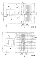
- Figure 3 is a top view of the embodiment according to Figure 1 .
- the location of the cross section shown in Figure 1 is indicated in Figure 3 by the horizontal dash-dotted line.
- Elements shown in Figure 3 that correspond to elements shown in Figure 1 are designated with the same reference numerals.
- the contact pad 8 is formed by the electrical conductor 4, which is partially covered by the dielectric layer 2 and/or the passivation layer 10.
- the outlines of the electrical conductor 4 and the further electrical conductor 5 are shown in Figure 3 by broken lines as hidden contours.
- the positions of the vertical interconnections 17 that are connected to the electrical conductor 4 and the further electrical conductor 5 are also indicated in Figure 3 .
- the further conductor 9 comprises a plurality of single conductors 19, each of which has the shape of an elongate ridge 12 with a longitudinal extension e.
- the longitudinal extensions e may especially be parallel to one another.
- the ridges 12 may all have the same size or may instead have different sizes, as shown in Figure 3 by way of example.
- the length d of a ridge 12, measured along its longitudinal extension e, exceeds its width w typically by a factor of at least three.
- Figure 4 is a top view of the arrangement according to Figure 2 and shows the arrangement of the nanotubes 11 extending across the single conductors 19 forming the further conductor 9.
- the other elements shown in Figure 4 correspond to the elements shown in Figure 3 and are designated with the same reference numerals.
- the parallel arrangement of the ridges 12 forming the single conductors 19 and the transverse parallel arrangement of the nanotubes 11 may be preferred in order to facilitate the connection of the nanotubes 11 with the further conductor 9.
- Figure 5 is a cross section of an intermediate product of the production method.
- the semiconductor substrate 1 is provided with the dielectric layer 2 including the wiring 3.
- Figure 5 does not show the passivation layer 10, which can optionally be applied on the dielectric layer 2 and does not essentially change the method steps.
- An opening 13 is formed in the dielectric layer 2 to uncover a contact pad 8 formed by one of the conductors 4, and a further opening 14 is formed in the dielectric layer 2 to uncover an area of a further one of the conductors 5, separate from the contact pad 8.
- the opening 13 and the further opening 14 can be formed in the same method step, especially by using a mask with windows in the areas where the opening 13 and the further opening 14 are to be formed.
- the further opening 14 may be a plurality of parallel trenches, for example. The length of the trenches is larger than the width of the trenches, typically by a factor of at least three.
- Figure 6 is a cross section according to Figure 5 after the application of an electrically conductive material 15, especially a material comprising a metal like tungsten or copper, which may form an entire layer.
- an electrically conductive material 15 especially a material comprising a metal like tungsten or copper, which may form an entire layer.
- a thin liner which may be TiN, for instance, and is not shown in Figure 6 , may be applied on the entire surface that is to be covered by the electrically conductive material 15.
- the further opening 14 is filled with the electrically conductive material 15, which thus forms the further conductor 9.
- the upper portion of the electrically conductive material 15 covering the upper surface of the dielectric layer 2 (or the passivation layer 10, if such is provided) is then removed.
- This may be effected by etching the electrically conductive material 15 selectively with respect to the dielectric layer 2 (or the passivation layer 10, if such is provided) and/or the liner, in particular by reactive ion etching (RIE).
- RIE reactive ion etching
- the etching step may produce slight depressions in the area of the further opening 14, which however remains at least half filled.
- the upper portion of the electrically conductive material 15 can instead be removed by chemical mechanical polishing (CMP), which yields an essentially planar surface with the further opening 14 remaining completely filled.
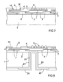
- Figure 7 is a cross section according to Figure 6 after the removal of the upper portion of the electrically conductive material 15 by selectively etching.
- the etching step is preferably performed anisotropically, so that a spacer 16 consisting of a residual portion of the electrically conductive material 15 is produced at the sidewall of the opening 13 above the contact pad 8.
- the dielectric layer 2 (or the passivation layer 10, if such is provided) is then thinned from the surface opposite to the semiconductor substrate 1, until the further conductor 9 protrudes from the dielectric layer 2 sufficiently far, and an embodiment similar to the one shown in Figure 1 is thus obtained.
- the semiconductor device can be produced within a standard CMOS process with only few additional method steps, which are furthermore fully compatible with the standard CMOS process.
- the protruding further conductor 9 facilitates an electrical connection to elements of a further device, especially to elements comprising a gas-sensitive material, like carbon nanotubes, for instance.
- Figure 8 is a cross section of a further embodiment of the semiconductor device comprising a through-substrate via.
- a via hole 20 is etched from the rear side into the semiconductor substrate 1, and a rear contact area of one of the conductors 6 of the wiring 3 is uncovered.
- a further dielectric layer 21 is formed to insulate the semiconductor material.
- a metallization 22 is arranged in the via hole 20 in contact with the rear contact area of the electrical conductor 6 of the wiring 3.
- the metallization 22 can be electrically connected with a further rear contact area 23 on a rear portion of the metallization, which is provided for an external electrical connection.
- a further passivation layer 24, which is opened above the contact area 23, may be applied on the rear side and on the metallization 22 within the via hole 20.
Landscapes
- Chemical & Material Sciences (AREA)
- Chemical Kinetics & Catalysis (AREA)
- Electrochemistry (AREA)
- Physics & Mathematics (AREA)
- Health & Medical Sciences (AREA)
- Life Sciences & Earth Sciences (AREA)
- Analytical Chemistry (AREA)
- Biochemistry (AREA)
- General Health & Medical Sciences (AREA)
- General Physics & Mathematics (AREA)
- Immunology (AREA)
- Pathology (AREA)
- Internal Circuitry In Semiconductor Integrated Circuit Devices (AREA)
Abstract
Description
-
US 5 767 001 discloses a semiconductor device for three-dimensional integration, which comprises contact pins penetrating a substrate and protruding from a rear surface. -
US 5 910 020 discloses a production method for semiconductor devices by forming a tungsten pillar on a wiring and applying an aluminum alloy to contact top and side surfaces of the tungsten pillar, which extend above a silicon oxide layer. - The publication of M.-S. Wang et al.: "Interface Dynamic Behavior Between a Carbon Nanotube and Metal Electrode," in Advanced Materials 22 (2010), pages 93 to 98 describes a contact between individual carbon nanotubes (CNTs) and sharpened tungsten electrodes. The tip-end of the electrode absorbs the source CNT atoms, which then penetrate deep into its body, form a carbide, and finally precipitate as freshly formed graphitic tubular shells encapsulating the electrode.
- It is an object of the present invention to disclose a semiconductor device that facilitates an electrical connection to nanotube structures. It is a further object to disclose a method of producing such a semiconductor device.
- This object is achieved with the semiconductor device according to
claim 1 and with the method of producing a semiconductor device according toclaim 10. Embodiments and variants derive from the dependent claims. - The semiconductor device comprises a semiconductor substrate, a dielectric layer on or above the substrate, a wiring comprising electrical conductors arranged in the dielectric layer, and a contact pad formed by one of the conductors. A further conductor of electrically conductive material is arranged in the dielectric layer in contact with a further one of the conductors, separate from the contact pad. The further conductor protrudes from the dielectric layer on a far side of the dielectric layer with respect to the substrate.
- An embodiment of the semiconductor device further comprises a passivation layer on the far side of the dielectric layer, and the further electrical conductor also protrudes from the passivation layer. The passivation layer and the dielectric layer comprise different materials. In particular, the dielectric layer may be a silicon oxide like SiO2 and the passivation layer a silicon nitride like Si3N4, for instance.
- In a further embodiment the further conductor has the shape of an elongate ridge with a longitudinal extension.
- In a further embodiment the ridge has a length along its longitudinal extension and a width transverse to its longitudinal extension, the length being at least three times the width.
- In a further embodiment the further conductor comprises a plurality of single conductors.
- In a further embodiment each of the single conductors has the shape of an elongate ridge with a longitudinal extension, and the longitudinal extensions are parallel to one another.
- In a further embodiment the further conductor comprises tungsten or copper.
- In a further embodiment the further conductor protrudes by a height in the range from 20 nm to 100 nm.
- A further embodiment comprises a via hole penetrating the semiconductor substrate and a metallization, which is arranged in the via hole and contacts one of the conductors, thus forming a through-substrate via.
- The method comprises forming a wiring of electrical conductors in a dielectric layer on or above a semiconductor substrate, an opening in the dielectric layer to uncover a contact pad, which is formed by one of the conductors, and a further opening in the dielectric layer to uncover an area of a further one of the conductors, separate from the contact pad. The further opening is filled with an electrically conductive material, and the dielectric layer is thinned from a side opposite the substrate, so that the electrically conductive material protrudes from the dielectric layer.
- In a variant of the method, the electrically conductive material is also filled in the opening uncovering the contact pad, and a portion of the electrically conductive material is removed such that a spacer is formed in the opening by a residual portion of the electrically conductive material while the further opening remains at least half filled.
- In a further variant of the method, the further opening is formed by a trench.
- In a further variant of the method, the further opening is formed by a plurality of parallel trenches.
- In a further variant of the method, the electrically conductive material filling the further opening comprises a metal that is different from the electrical conductors.
- The following is a detailed description of examples of the semiconductor device and the production method in conjunction with the appended figures.
- Figure 1
- is a cross section of an embodiment of the semiconductor device.
- Figure 2
- is a cross section according to
Figure 1 including an arrangement of nanotubes. - Figure 3
- is a top view of the embodiment according to
Figure 1 . - Figure 4
- is a top view of the arrangement according to
Figure 2 . - Figure 5
- is a cross section of an intermediate product of the production method.
- Figure 6
- is a cross section according to
Figure 5 after the application of an electrically conductive material. - Figure 7
- is a cross section according to
Figure 6 after a partial removal of the electrically conductive material. - Figure 8
- is a cross section of a further embodiment of the semiconductor device comprising a through-substrate via.
-
Figure 1 is a cross section of an embodiment of the semiconductor device comprising asemiconductor substrate 1, which may be silicon, for instance, adielectric layer 2 on thesemiconductor substrate 1, and a wiring 3 embedded in thedielectric layer 2, which may be a silicon oxide, especially silicon dioxide, for instance. The wiring 3 comprises electrical conductors, which may especially be formed bystructured metal layers 6 andvertical interconnections 7 like metal plugs, for instance. The wiring 3 may be provided for an integrated circuit like a CMOS circuit integrated in thesemiconductor substrate 1. Acontact pad 8 is formed by one of theelectrical conductors 4, which may typically belong to an uppermost metallization layer. - A further one of the
electrical conductors 5, which is separate from thecontact pad 8, is provided with a furtherelectrical conductor 9, which protrudes from thedielectric layer 2 on the far side with respect to thesemiconductor substrate 1. Apassivation layer 10, which can especially be formed from a material different from the material of thedielectric layer 2 and may comprise a silicon nitride like Si3N4, for instance, can be applied on thedielectric layer 2 as shown inFigure 1 . If apassivation layer 10 is present, thefurther conductor 9 also protrudes from thepassivation layer 10. The height h by which thefurther conductor 9 protrudes may be typically in the range from 20 nm to 100 nm. Thecontact pad 8 may be provided in standard fashion with further electrically conductive material like anunderbump metallization 18, for instance. -
Figure 2 is a cross section according toFigure 1 and schematically indicates an arrangement of the semiconductor device with a further device, which may especially be a gas sensor, a chemical sensor or a humidity sensor, which may be provided with a gas-sensitive material like SnO2 or carbon nanotubes.Figure 2 shows a parallel arrangement ofnanotubes 11 contacting the protruding tips of thefurther conductor 9, by way of example. -
Figure 3 is a top view of the embodiment according toFigure 1 . The location of the cross section shown inFigure 1 is indicated inFigure 3 by the horizontal dash-dotted line. Elements shown inFigure 3 that correspond to elements shown inFigure 1 are designated with the same reference numerals. Thecontact pad 8 is formed by theelectrical conductor 4, which is partially covered by thedielectric layer 2 and/or thepassivation layer 10. The outlines of theelectrical conductor 4 and the furtherelectrical conductor 5 are shown inFigure 3 by broken lines as hidden contours. The positions of thevertical interconnections 17 that are connected to theelectrical conductor 4 and the furtherelectrical conductor 5 are also indicated inFigure 3 . In the embodiment according toFigures 1 and3 , thefurther conductor 9 comprises a plurality ofsingle conductors 19, each of which has the shape of anelongate ridge 12 with a longitudinal extension e. The longitudinal extensions e may especially be parallel to one another. Theridges 12 may all have the same size or may instead have different sizes, as shown inFigure 3 by way of example. The length d of aridge 12, measured along its longitudinal extension e, exceeds its width w typically by a factor of at least three. -
Figure 4 is a top view of the arrangement according toFigure 2 and shows the arrangement of thenanotubes 11 extending across thesingle conductors 19 forming thefurther conductor 9. The other elements shown inFigure 4 correspond to the elements shown inFigure 3 and are designated with the same reference numerals. The parallel arrangement of theridges 12 forming thesingle conductors 19 and the transverse parallel arrangement of thenanotubes 11 may be preferred in order to facilitate the connection of thenanotubes 11 with thefurther conductor 9. -
Figure 5 is a cross section of an intermediate product of the production method. Thesemiconductor substrate 1 is provided with thedielectric layer 2 including the wiring 3.Figure 5 does not show thepassivation layer 10, which can optionally be applied on thedielectric layer 2 and does not essentially change the method steps. Anopening 13 is formed in thedielectric layer 2 to uncover acontact pad 8 formed by one of theconductors 4, and afurther opening 14 is formed in thedielectric layer 2 to uncover an area of a further one of theconductors 5, separate from thecontact pad 8. Theopening 13 and thefurther opening 14 can be formed in the same method step, especially by using a mask with windows in the areas where theopening 13 and thefurther opening 14 are to be formed. In particular, thefurther opening 14 may be a plurality of parallel trenches, for example. The length of the trenches is larger than the width of the trenches, typically by a factor of at least three. -
Figure 6 is a cross section according toFigure 5 after the application of an electricallyconductive material 15, especially a material comprising a metal like tungsten or copper, which may form an entire layer. Before the electricallyconductive material 15 is applied, a thin liner, which may be TiN, for instance, and is not shown inFigure 6 , may be applied on the entire surface that is to be covered by the electricallyconductive material 15. Thefurther opening 14 is filled with the electricallyconductive material 15, which thus forms thefurther conductor 9. The upper portion of the electricallyconductive material 15 covering the upper surface of the dielectric layer 2 (or thepassivation layer 10, if such is provided) is then removed. This may be effected by etching the electricallyconductive material 15 selectively with respect to the dielectric layer 2 (or thepassivation layer 10, if such is provided) and/or the liner, in particular by reactive ion etching (RIE). The etching step may produce slight depressions in the area of thefurther opening 14, which however remains at least half filled. The upper portion of the electricallyconductive material 15 can instead be removed by chemical mechanical polishing (CMP), which yields an essentially planar surface with thefurther opening 14 remaining completely filled. -
Figure 7 is a cross section according toFigure 6 after the removal of the upper portion of the electricallyconductive material 15 by selectively etching. The etching step is preferably performed anisotropically, so that aspacer 16 consisting of a residual portion of the electricallyconductive material 15 is produced at the sidewall of theopening 13 above thecontact pad 8. The dielectric layer 2 (or thepassivation layer 10, if such is provided) is then thinned from the surface opposite to thesemiconductor substrate 1, until thefurther conductor 9 protrudes from thedielectric layer 2 sufficiently far, and an embodiment similar to the one shown inFigure 1 is thus obtained. - By the described method the semiconductor device can be produced within a standard CMOS process with only few additional method steps, which are furthermore fully compatible with the standard CMOS process. The protruding
further conductor 9 facilitates an electrical connection to elements of a further device, especially to elements comprising a gas-sensitive material, like carbon nanotubes, for instance. -
Figure 8 is a cross section of a further embodiment of the semiconductor device comprising a through-substrate via. A viahole 20 is etched from the rear side into thesemiconductor substrate 1, and a rear contact area of one of theconductors 6 of the wiring 3 is uncovered. Afurther dielectric layer 21 is formed to insulate the semiconductor material. Ametallization 22 is arranged in the viahole 20 in contact with the rear contact area of theelectrical conductor 6 of the wiring 3. Themetallization 22 can be electrically connected with a furtherrear contact area 23 on a rear portion of the metallization, which is provided for an external electrical connection. Thus an electrical interconnection penetrating thesemiconductor substrate 1 is formed. Afurther passivation layer 24, which is opened above thecontact area 23, may be applied on the rear side and on themetallization 22 within the viahole 20. -
- 1
- semiconductor substrate
- 2
- dielectric layer
- 3
- wiring
- 4
- electrical conductor
- 5
- further electrical conductor
- 6
- metal layer
- 7
- vertical interconnection
- 8
- contact pad
- 9
- further conductor
- 10
- passivation layer
- 11
- nanotube
- 12
- ridge
- 13
- opening
- 14
- further opening
- 15
- electrically conductive material
- 16
- spacer
- 17
- vertical interconnection
- 18
- underbump metallization
- 19
- single conductor
- 20
- via hole
- 21
- further dielectric layer
- 22
- metallization
- 23
- contact area
- 24
- further passivation layer
- d
- length
- e
- longitudinal direction
- h
- height
- w
- width
Claims (14)
- A semiconductor device, comprising:- a semiconductor substrate (1),- a dielectric layer (2) on or above the substrate (1),- a wiring (3) comprising electrical conductors (4, 5, 6, 7) arranged in the dielectric layer (2), and- a contact pad (8) formed by one of the conductors (4), characterized in that- a further conductor (9) of electrically conductive material is arranged in the dielectric layer (2) in contact with a further one of the conductors (5), separate from the contact pad (8), and- the further conductor (9) protrudes from the dielectric layer (2) on a far side of the dielectric layer (2) with respect to the substrate (1).
- The semiconductor device of claim 1, further comprising:a passivation layer (10) on the far side of the dielectric layer (2), the passivation layer (10) and the dielectric layer (2) comprising different materials, the further electrical conductor (9) protruding from the passivation layer (10).
- The semiconductor device of claim 1 or 2, wherein the further conductor (9) has the shape of an elongate ridge (12) with a longitudinal extension (e).
- The semiconductor device of claim 3, wherein the ridge (12) has a length (d) along its longitudinal extension (e) and a width (w) transverse to its longitudinal extension (e), the length (d) being at least three times the width (w).
- The semiconductor device of claim 1 or 2, wherein the further conductor (9) comprises a plurality of single conductors (19).
- The semiconductor device of claim 5, wherein each of the single conductors (19) has the shape of an elongate ridge (12) with a longitudinal extension (e), and the longitudinal extensions (e) are parallel to one another.
- The semiconductor device of one of claims 1 to 6, wherein the further conductor (9) comprises tungsten or copper.
- The semiconductor device of one of claims 1 to 7, wherein the further conductor (9) protrudes by a height (h) in the range from 20 nm to 100 nm.
- The semiconductor device of one of claims 1 to 8, further comprising:- a via hole (20) penetrating the semiconductor substrate (1), and- a metallization (22) arranged in the via hole (20) and contacting one of the conductors (6), thus forming a through-substrate via.
- A method of producing a semiconductor device, comprising:- forming a wiring (3) comprising electrical conductors (4, 5, 6, 7) in a dielectric layer (2) on or above a semiconductor substrate (1), and- forming an opening (13) in the dielectric layer (2) to uncover a contact pad (8) formed by one of the conductors (4),
characterized in that- a further opening (14) is formed in the dielectric layer (2) and an area of a further one of the conductors (5), separate from the contact pad (8), is thus uncovered,- the further opening (14) is filled with an electrically conductive material (15), and- the dielectric layer (2) is thinned from a side opposite the substrate (1), so that the electrically conductive material (15) protrudes from the dielectric layer (2). - The method of claim 10, wherein- the electrically conductive material (15) is also filled in the opening (13) uncovering the contact pad (8), and- a portion of the electrically conductive material (15) is removed such that a spacer (16) is formed in the opening (13) by a residual portion of the electrically conductive material (15) and the further opening (14) remains at least half filled.
- The method of claim 10 or 11, wherein the further opening (14) is formed by a trench.
- The method of claim 10 or 11, wherein the further opening (14) is formed by a plurality of parallel trenches.
- The method of one of claims 10 to 13, wherein the electrically conductive material (15) filling the further opening (14) comprises a metal that is different from the electrical conductors (4, 5, 6, 7).
Priority Applications (4)
| Application Number | Priority Date | Filing Date | Title |
|---|---|---|---|
| EP14154132.6A EP2905611B1 (en) | 2014-02-06 | 2014-02-06 | Method of producing a semiconductor device with protruding contacts |
| CN201580007271.2A CN105980840B (en) | 2014-02-06 | 2015-01-14 | Manufacture the method with the semiconductor devices of projection contacts |
| PCT/EP2015/050592 WO2015117800A1 (en) | 2014-02-06 | 2015-01-14 | Method of producing a semiconductor device with protruding contacts |
| US15/117,175 US9768131B2 (en) | 2014-02-06 | 2015-01-14 | Method of producing a semiconductor device with protruding contacts |
Applications Claiming Priority (1)
| Application Number | Priority Date | Filing Date | Title |
|---|---|---|---|
| EP14154132.6A EP2905611B1 (en) | 2014-02-06 | 2014-02-06 | Method of producing a semiconductor device with protruding contacts |
Publications (2)
| Publication Number | Publication Date |
|---|---|
| EP2905611A1 true EP2905611A1 (en) | 2015-08-12 |
| EP2905611B1 EP2905611B1 (en) | 2018-01-17 |
Family
ID=50064476
Family Applications (1)
| Application Number | Title | Priority Date | Filing Date |
|---|---|---|---|
| EP14154132.6A Active EP2905611B1 (en) | 2014-02-06 | 2014-02-06 | Method of producing a semiconductor device with protruding contacts |
Country Status (4)
| Country | Link |
|---|---|
| US (1) | US9768131B2 (en) |
| EP (1) | EP2905611B1 (en) |
| CN (1) | CN105980840B (en) |
| WO (1) | WO2015117800A1 (en) |
Families Citing this family (2)
| Publication number | Priority date | Publication date | Assignee | Title |
|---|---|---|---|---|
| US20200333284A1 (en) * | 2019-04-18 | 2020-10-22 | Honeywell International Inc. | High surface area electrode for electrochemical sensor |
| US11424198B2 (en) * | 2020-09-01 | 2022-08-23 | Nanya Technology Corporation | Semiconductor device with graphene layers and method for fabricating the same |
Citations (4)
| Publication number | Priority date | Publication date | Assignee | Title |
|---|---|---|---|---|
| US5767001A (en) | 1993-05-05 | 1998-06-16 | Siemens Aktiengesellschaft | Process for producing semiconductor components between which contact is made vertically |
| US5910020A (en) | 1995-12-18 | 1999-06-08 | Nec Corporation | Method for fabricating a semiconductor device having a refractory metal pillar for electrical connection |
| US20090200664A1 (en) * | 2007-12-17 | 2009-08-13 | Tatsuo Migita | Manufacturing method of semiconductor apparatus and semiconductor apparatus |
| EP2554980A1 (en) * | 2011-08-03 | 2013-02-06 | Nxp B.V. | Integrated circuit with sensor and method of manufacturing such an integrated circuit |
Family Cites Families (10)
| Publication number | Priority date | Publication date | Assignee | Title |
|---|---|---|---|---|
| DE2032872B2 (en) * | 1970-07-02 | 1975-03-20 | Siemens Ag, 1000 Berlin Und 8000 Muenchen | Process for the production of soft solderable contacts for the installation of semiconductor components in housings |
| US5055426A (en) | 1990-09-10 | 1991-10-08 | Micron Technology, Inc. | Method for forming a multilevel interconnect structure on a semiconductor wafer |
| DE10307815B3 (en) | 2003-02-24 | 2004-11-11 | Infineon Technologies Ag | Integrated electronic component with specifically created nanotubes in vertical structures and its manufacturing process |
| US6955937B1 (en) | 2004-08-12 | 2005-10-18 | Lsi Logic Corporation | Carbon nanotube memory cell for integrated circuit structure with removable side spacers to permit access to memory cell and process for forming such memory cell |
| US7851348B2 (en) * | 2005-06-14 | 2010-12-14 | Abhay Misra | Routingless chip architecture |
| WO2007105535A1 (en) * | 2006-03-14 | 2007-09-20 | Matsushita Electric Industrial Co., Ltd. | Electronic part mounting structure and its manufacturing method |
| US7863189B2 (en) * | 2007-01-05 | 2011-01-04 | International Business Machines Corporation | Methods for fabricating silicon carriers with conductive through-vias with low stress and low defect density |
| CN101638212A (en) * | 2009-09-08 | 2010-02-03 | 华中科技大学 | Wafer-level vacuum encapsulation wire interconnecting structure of micro electro mechanical system and manufacturing method thereof |
| US8587120B2 (en) * | 2011-06-23 | 2013-11-19 | Stats Chippac, Ltd. | Semiconductor device and method of forming interconnect structure over seed layer on contact pad of semiconductor die without undercutting seed layer beneath interconnect structure |
| US9053989B2 (en) | 2011-09-08 | 2015-06-09 | Taiwan Semiconductor Manufacturing Company, Ltd. | Elongated bump structure in semiconductor device |
-
2014
- 2014-02-06 EP EP14154132.6A patent/EP2905611B1/en active Active
-
2015
- 2015-01-14 WO PCT/EP2015/050592 patent/WO2015117800A1/en not_active Ceased
- 2015-01-14 CN CN201580007271.2A patent/CN105980840B/en active Active
- 2015-01-14 US US15/117,175 patent/US9768131B2/en active Active
Patent Citations (4)
| Publication number | Priority date | Publication date | Assignee | Title |
|---|---|---|---|---|
| US5767001A (en) | 1993-05-05 | 1998-06-16 | Siemens Aktiengesellschaft | Process for producing semiconductor components between which contact is made vertically |
| US5910020A (en) | 1995-12-18 | 1999-06-08 | Nec Corporation | Method for fabricating a semiconductor device having a refractory metal pillar for electrical connection |
| US20090200664A1 (en) * | 2007-12-17 | 2009-08-13 | Tatsuo Migita | Manufacturing method of semiconductor apparatus and semiconductor apparatus |
| EP2554980A1 (en) * | 2011-08-03 | 2013-02-06 | Nxp B.V. | Integrated circuit with sensor and method of manufacturing such an integrated circuit |
Non-Patent Citations (3)
| Title |
|---|
| HELBLING T ET AL: "Sensing NO2 with individual suspended single-walled carbon nanotubes", SENSORS AND ACTUATORS B: CHEMICAL: INTERNATIONAL JOURNAL DEVOTED TO RESEARCH AND DEVELOPMENT OF PHYSICAL AND CHEMICAL TRANSDUCERS, ELSEVIER S.A, CH, vol. 132, no. 2, 16 June 2008 (2008-06-16), pages 491 - 497, XP022707541, ISSN: 0925-4005, [retrieved on 20071126], DOI: 10.1016/J.SNB.2007.11.036 * |
| M.-S. WANG ET AL.: "Interface Dynamic Behavior Between a Carbon Nanotube and Metal Electrode", ADVANCED MATERIALS, vol. 22, 2010, pages 93 - 98 |
| SAMEER SONKUSALE ET AL: "Heterogeneous integration of carbon nanotubes and graphene microassemblies for environmental and breath sensing", DESIGN AUTOMATION CONFERENCE (DAC), 2011 48TH ACM/EDAC/IEEE, IEEE, 5 June 2011 (2011-06-05), pages 723 - 728, XP031927800, ISBN: 978-1-4503-0636-2 * |
Also Published As
| Publication number | Publication date |
|---|---|
| WO2015117800A1 (en) | 2015-08-13 |
| EP2905611B1 (en) | 2018-01-17 |
| US20160351515A1 (en) | 2016-12-01 |
| CN105980840A (en) | 2016-09-28 |
| US9768131B2 (en) | 2017-09-19 |
| CN105980840B (en) | 2019-07-16 |
Similar Documents
| Publication | Publication Date | Title |
|---|---|---|
| DE102012208033B4 (en) | Hybrid integrated component and method for its production | |
| US8710648B2 (en) | Wafer level packaging structure with large contact area and preparation method thereof | |
| US20150380313A1 (en) | Method of forming semiconductor structure with horizontal gate all around structure | |
| US8349674B2 (en) | Forming borderless contact for transistors in a replacement metal gate process | |
| WO2009142982A3 (en) | Metal gate structure and method of manufacturing same | |
| US8987862B2 (en) | Methods of forming semiconductor devices having conductors with different dimensions | |
| JP2008537335A5 (en) | ||
| US9012329B2 (en) | Nanogap in-between noble metals | |
| CN104854694A (en) | Devices, systems, and methods related to forming through-substrate vias with sacrificial plugs | |
| TW201904864A (en) | Stacked elongated nanoshapes of different semiconductor materials and structures that incorporate the nanoshapes | |
| JP6969586B2 (en) | Semiconductor devices and their manufacturing methods | |
| KR20160021559A (en) | Capacitive micromachined ultrasonic transducer having nanopilar structure and method of fabricating the same | |
| CN108695382B (en) | Semiconductor device and method of manufacturing the same | |
| JP2009164481A5 (en) | ||
| CN107683528B (en) | High-density capacitors formed from thin vertical semiconductor structures such as FINFETs | |
| CN105304566B (en) | A kind of semiconductor devices and its manufacturing method, electronic device | |
| US11167982B2 (en) | Semiconductor arrangement and formation thereof | |
| EP2905611B1 (en) | Method of producing a semiconductor device with protruding contacts | |
| EP2693467A1 (en) | A method of producing a semiconductor device having an interconnect through the substrate | |
| US8878314B2 (en) | MEMS package or sensor package with intra-cap electrical via and method thereof | |
| EP2905253A2 (en) | Fluid sensor with backside of sensor die contacting header | |
| US10941033B2 (en) | 3D stack configuration for 6-axis motion sensor | |
| US20170154970A1 (en) | Buried Bus and Related Method | |
| US20160240776A1 (en) | Memory device and method for fabricating the same | |
| CN104253022A (en) | Electric field gap device and manufacturing method |
Legal Events
| Date | Code | Title | Description |
|---|---|---|---|
| PUAI | Public reference made under article 153(3) epc to a published international application that has entered the european phase |
Free format text: ORIGINAL CODE: 0009012 |
|
| AK | Designated contracting states |
Kind code of ref document: A1 Designated state(s): AL AT BE BG CH CY CZ DE DK EE ES FI FR GB GR HR HU IE IS IT LI LT LU LV MC MK MT NL NO PL PT RO RS SE SI SK SM TR |
|
| AX | Request for extension of the european patent |
Extension state: BA ME |
|
| 17P | Request for examination filed |
Effective date: 20160121 |
|
| RBV | Designated contracting states (corrected) |
Designated state(s): AL AT BE BG CH CY CZ DE DK EE ES FI FR GB GR HR HU IE IS IT LI LT LU LV MC MK MT NL NO PL PT RO RS SE SI SK SM TR |
|
| GRAP | Despatch of communication of intention to grant a patent |
Free format text: ORIGINAL CODE: EPIDOSNIGR1 |
|
| INTG | Intention to grant announced |
Effective date: 20170814 |
|
| GRAS | Grant fee paid |
Free format text: ORIGINAL CODE: EPIDOSNIGR3 |
|
| GRAA | (expected) grant |
Free format text: ORIGINAL CODE: 0009210 |
|
| AK | Designated contracting states |
Kind code of ref document: B1 Designated state(s): AL AT BE BG CH CY CZ DE DK EE ES FI FR GB GR HR HU IE IS IT LI LT LU LV MC MK MT NL NO PL PT RO RS SE SI SK SM TR |
|
| REG | Reference to a national code |
Ref country code: GB Ref legal event code: FG4D |
|
| RIN1 | Information on inventor provided before grant (corrected) |
Inventor name: SCHREMS, MARTIN Inventor name: ROHRACHER, KARL Inventor name: KRAFT, JOCHEN |
|
| REG | Reference to a national code |
Ref country code: CH Ref legal event code: EP |
|
| REG | Reference to a national code |
Ref country code: IE Ref legal event code: FG4D |
|
| REG | Reference to a national code |
Ref country code: AT Ref legal event code: REF Ref document number: 964761 Country of ref document: AT Kind code of ref document: T Effective date: 20180215 |
|
| REG | Reference to a national code |
Ref country code: DE Ref legal event code: R096 Ref document number: 602014019960 Country of ref document: DE |
|
| REG | Reference to a national code |
Ref country code: FR Ref legal event code: PLFP Year of fee payment: 5 |
|
| REG | Reference to a national code |
Ref country code: NL Ref legal event code: MP Effective date: 20180117 |
|
| REG | Reference to a national code |
Ref country code: LT Ref legal event code: MG4D |
|
| REG | Reference to a national code |
Ref country code: AT Ref legal event code: MK05 Ref document number: 964761 Country of ref document: AT Kind code of ref document: T Effective date: 20180117 |
|
| PG25 | Lapsed in a contracting state [announced via postgrant information from national office to epo] |
Ref country code: NL Free format text: LAPSE BECAUSE OF FAILURE TO SUBMIT A TRANSLATION OF THE DESCRIPTION OR TO PAY THE FEE WITHIN THE PRESCRIBED TIME-LIMIT Effective date: 20180117 |
|
| PG25 | Lapsed in a contracting state [announced via postgrant information from national office to epo] |
Ref country code: NO Free format text: LAPSE BECAUSE OF FAILURE TO SUBMIT A TRANSLATION OF THE DESCRIPTION OR TO PAY THE FEE WITHIN THE PRESCRIBED TIME-LIMIT Effective date: 20180417 Ref country code: FI Free format text: LAPSE BECAUSE OF FAILURE TO SUBMIT A TRANSLATION OF THE DESCRIPTION OR TO PAY THE FEE WITHIN THE PRESCRIBED TIME-LIMIT Effective date: 20180117 Ref country code: HR Free format text: LAPSE BECAUSE OF FAILURE TO SUBMIT A TRANSLATION OF THE DESCRIPTION OR TO PAY THE FEE WITHIN THE PRESCRIBED TIME-LIMIT Effective date: 20180117 Ref country code: CY Free format text: LAPSE BECAUSE OF FAILURE TO SUBMIT A TRANSLATION OF THE DESCRIPTION OR TO PAY THE FEE WITHIN THE PRESCRIBED TIME-LIMIT Effective date: 20180117 Ref country code: LT Free format text: LAPSE BECAUSE OF FAILURE TO SUBMIT A TRANSLATION OF THE DESCRIPTION OR TO PAY THE FEE WITHIN THE PRESCRIBED TIME-LIMIT Effective date: 20180117 Ref country code: ES Free format text: LAPSE BECAUSE OF FAILURE TO SUBMIT A TRANSLATION OF THE DESCRIPTION OR TO PAY THE FEE WITHIN THE PRESCRIBED TIME-LIMIT Effective date: 20180117 |
|
| PG25 | Lapsed in a contracting state [announced via postgrant information from national office to epo] |
Ref country code: GR Free format text: LAPSE BECAUSE OF FAILURE TO SUBMIT A TRANSLATION OF THE DESCRIPTION OR TO PAY THE FEE WITHIN THE PRESCRIBED TIME-LIMIT Effective date: 20180418 Ref country code: BG Free format text: LAPSE BECAUSE OF FAILURE TO SUBMIT A TRANSLATION OF THE DESCRIPTION OR TO PAY THE FEE WITHIN THE PRESCRIBED TIME-LIMIT Effective date: 20180417 Ref country code: IS Free format text: LAPSE BECAUSE OF FAILURE TO SUBMIT A TRANSLATION OF THE DESCRIPTION OR TO PAY THE FEE WITHIN THE PRESCRIBED TIME-LIMIT Effective date: 20180517 Ref country code: LV Free format text: LAPSE BECAUSE OF FAILURE TO SUBMIT A TRANSLATION OF THE DESCRIPTION OR TO PAY THE FEE WITHIN THE PRESCRIBED TIME-LIMIT Effective date: 20180117 Ref country code: SE Free format text: LAPSE BECAUSE OF FAILURE TO SUBMIT A TRANSLATION OF THE DESCRIPTION OR TO PAY THE FEE WITHIN THE PRESCRIBED TIME-LIMIT Effective date: 20180117 Ref country code: AT Free format text: LAPSE BECAUSE OF FAILURE TO SUBMIT A TRANSLATION OF THE DESCRIPTION OR TO PAY THE FEE WITHIN THE PRESCRIBED TIME-LIMIT Effective date: 20180117 Ref country code: RS Free format text: LAPSE BECAUSE OF FAILURE TO SUBMIT A TRANSLATION OF THE DESCRIPTION OR TO PAY THE FEE WITHIN THE PRESCRIBED TIME-LIMIT Effective date: 20180117 Ref country code: PL Free format text: LAPSE BECAUSE OF FAILURE TO SUBMIT A TRANSLATION OF THE DESCRIPTION OR TO PAY THE FEE WITHIN THE PRESCRIBED TIME-LIMIT Effective date: 20180117 |
|
| REG | Reference to a national code |
Ref country code: CH Ref legal event code: PL |
|
| REG | Reference to a national code |
Ref country code: DE Ref legal event code: R097 Ref document number: 602014019960 Country of ref document: DE |
|
| PG25 | Lapsed in a contracting state [announced via postgrant information from national office to epo] |
Ref country code: RO Free format text: LAPSE BECAUSE OF FAILURE TO SUBMIT A TRANSLATION OF THE DESCRIPTION OR TO PAY THE FEE WITHIN THE PRESCRIBED TIME-LIMIT Effective date: 20180117 Ref country code: EE Free format text: LAPSE BECAUSE OF FAILURE TO SUBMIT A TRANSLATION OF THE DESCRIPTION OR TO PAY THE FEE WITHIN THE PRESCRIBED TIME-LIMIT Effective date: 20180117 Ref country code: IT Free format text: LAPSE BECAUSE OF FAILURE TO SUBMIT A TRANSLATION OF THE DESCRIPTION OR TO PAY THE FEE WITHIN THE PRESCRIBED TIME-LIMIT Effective date: 20180117 Ref country code: MC Free format text: LAPSE BECAUSE OF FAILURE TO SUBMIT A TRANSLATION OF THE DESCRIPTION OR TO PAY THE FEE WITHIN THE PRESCRIBED TIME-LIMIT Effective date: 20180117 Ref country code: AL Free format text: LAPSE BECAUSE OF FAILURE TO SUBMIT A TRANSLATION OF THE DESCRIPTION OR TO PAY THE FEE WITHIN THE PRESCRIBED TIME-LIMIT Effective date: 20180117 |
|
| PLBE | No opposition filed within time limit |
Free format text: ORIGINAL CODE: 0009261 |
|
| STAA | Information on the status of an ep patent application or granted ep patent |
Free format text: STATUS: NO OPPOSITION FILED WITHIN TIME LIMIT |
|
| REG | Reference to a national code |
Ref country code: IE Ref legal event code: MM4A |
|
| REG | Reference to a national code |
Ref country code: BE Ref legal event code: MM Effective date: 20180228 |
|
| PG25 | Lapsed in a contracting state [announced via postgrant information from national office to epo] |
Ref country code: LI Free format text: LAPSE BECAUSE OF NON-PAYMENT OF DUE FEES Effective date: 20180228 Ref country code: CH Free format text: LAPSE BECAUSE OF NON-PAYMENT OF DUE FEES Effective date: 20180228 Ref country code: LU Free format text: LAPSE BECAUSE OF NON-PAYMENT OF DUE FEES Effective date: 20180206 Ref country code: SK Free format text: LAPSE BECAUSE OF FAILURE TO SUBMIT A TRANSLATION OF THE DESCRIPTION OR TO PAY THE FEE WITHIN THE PRESCRIBED TIME-LIMIT Effective date: 20180117 Ref country code: CZ Free format text: LAPSE BECAUSE OF FAILURE TO SUBMIT A TRANSLATION OF THE DESCRIPTION OR TO PAY THE FEE WITHIN THE PRESCRIBED TIME-LIMIT Effective date: 20180117 Ref country code: DK Free format text: LAPSE BECAUSE OF FAILURE TO SUBMIT A TRANSLATION OF THE DESCRIPTION OR TO PAY THE FEE WITHIN THE PRESCRIBED TIME-LIMIT Effective date: 20180117 Ref country code: SM Free format text: LAPSE BECAUSE OF FAILURE TO SUBMIT A TRANSLATION OF THE DESCRIPTION OR TO PAY THE FEE WITHIN THE PRESCRIBED TIME-LIMIT Effective date: 20180117 |
|
| 26N | No opposition filed |
Effective date: 20181018 |
|
| GBPC | Gb: european patent ceased through non-payment of renewal fee |
Effective date: 20180417 |
|
| PG25 | Lapsed in a contracting state [announced via postgrant information from national office to epo] |
Ref country code: IE Free format text: LAPSE BECAUSE OF NON-PAYMENT OF DUE FEES Effective date: 20180206 |
|
| PG25 | Lapsed in a contracting state [announced via postgrant information from national office to epo] |
Ref country code: SI Free format text: LAPSE BECAUSE OF FAILURE TO SUBMIT A TRANSLATION OF THE DESCRIPTION OR TO PAY THE FEE WITHIN THE PRESCRIBED TIME-LIMIT Effective date: 20180117 Ref country code: GB Free format text: LAPSE BECAUSE OF NON-PAYMENT OF DUE FEES Effective date: 20180417 Ref country code: BE Free format text: LAPSE BECAUSE OF NON-PAYMENT OF DUE FEES Effective date: 20180228 |
|
| PG25 | Lapsed in a contracting state [announced via postgrant information from national office to epo] |
Ref country code: MT Free format text: LAPSE BECAUSE OF NON-PAYMENT OF DUE FEES Effective date: 20180206 |
|
| PG25 | Lapsed in a contracting state [announced via postgrant information from national office to epo] |
Ref country code: TR Free format text: LAPSE BECAUSE OF FAILURE TO SUBMIT A TRANSLATION OF THE DESCRIPTION OR TO PAY THE FEE WITHIN THE PRESCRIBED TIME-LIMIT Effective date: 20180117 |
|
| PG25 | Lapsed in a contracting state [announced via postgrant information from national office to epo] |
Ref country code: PT Free format text: LAPSE BECAUSE OF FAILURE TO SUBMIT A TRANSLATION OF THE DESCRIPTION OR TO PAY THE FEE WITHIN THE PRESCRIBED TIME-LIMIT Effective date: 20180117 |
|
| PG25 | Lapsed in a contracting state [announced via postgrant information from national office to epo] |
Ref country code: MK Free format text: LAPSE BECAUSE OF NON-PAYMENT OF DUE FEES Effective date: 20180117 Ref country code: HU Free format text: LAPSE BECAUSE OF FAILURE TO SUBMIT A TRANSLATION OF THE DESCRIPTION OR TO PAY THE FEE WITHIN THE PRESCRIBED TIME-LIMIT; INVALID AB INITIO Effective date: 20140206 |
|
| P01 | Opt-out of the competence of the unified patent court (upc) registered |
Effective date: 20230822 |
|
| PGFP | Annual fee paid to national office [announced via postgrant information from national office to epo] |
Ref country code: DE Payment date: 20260218 Year of fee payment: 13 |
|
| PGFP | Annual fee paid to national office [announced via postgrant information from national office to epo] |
Ref country code: FR Payment date: 20260218 Year of fee payment: 13 |