EP2903255B1 - Videosignalabschlusserkennungsschaltung - Google Patents
Videosignalabschlusserkennungsschaltung Download PDFInfo
- Publication number
- EP2903255B1 EP2903255B1 EP15153508.5A EP15153508A EP2903255B1 EP 2903255 B1 EP2903255 B1 EP 2903255B1 EP 15153508 A EP15153508 A EP 15153508A EP 2903255 B1 EP2903255 B1 EP 2903255B1
- Authority
- EP
- European Patent Office
- Prior art keywords
- video
- video signal
- signal
- receiver
- test voltage
- Prior art date
- Legal status (The legal status is an assumption and is not a legal conclusion. Google has not performed a legal analysis and makes no representation as to the accuracy of the status listed.)
- Active
Links
Images


Classifications
-
- H—ELECTRICITY
- H04—ELECTRIC COMMUNICATION TECHNIQUE
- H04N—PICTORIAL COMMUNICATION, e.g. TELEVISION
- H04N5/00—Details of television systems
- H04N5/222—Studio circuitry; Studio devices; Studio equipment
- H04N5/262—Studio circuits, e.g. for mixing, switching-over, change of character of image, other special effects ; Cameras specially adapted for the electronic generation of special effects
- H04N5/268—Signal distribution or switching
-
- G—PHYSICS
- G06—COMPUTING OR CALCULATING; COUNTING
- G06F—ELECTRIC DIGITAL DATA PROCESSING
- G06F13/00—Interconnection of, or transfer of information or other signals between, memories, input/output devices or central processing units
- G06F13/38—Information transfer, e.g. on bus
- G06F13/40—Bus structure
- G06F13/4063—Device-to-bus coupling
- G06F13/4068—Electrical coupling
- G06F13/4086—Bus impedance matching, e.g. termination
-
- H—ELECTRICITY
- H04—ELECTRIC COMMUNICATION TECHNIQUE
- H04N—PICTORIAL COMMUNICATION, e.g. TELEVISION
- H04N23/00—Cameras or camera modules comprising electronic image sensors; Control thereof
- H04N23/80—Camera processing pipelines; Components thereof
- H04N23/81—Camera processing pipelines; Components thereof for suppressing or minimising disturbance in the image signal generation
-
- H—ELECTRICITY
- H04—ELECTRIC COMMUNICATION TECHNIQUE
- H04N—PICTORIAL COMMUNICATION, e.g. TELEVISION
- H04N9/00—Details of colour television systems
- H04N9/64—Circuits for processing colour signals
- H04N9/642—Multi-standard receivers
-
- H—ELECTRICITY
- H04—ELECTRIC COMMUNICATION TECHNIQUE
- H04N—PICTORIAL COMMUNICATION, e.g. TELEVISION
- H04N5/00—Details of television systems
- H04N5/76—Television signal recording
- H04N5/765—Interface circuits between an apparatus for recording and another apparatus
- H04N5/77—Interface circuits between an apparatus for recording and another apparatus between a recording apparatus and a television camera
Definitions
- the present disclosure relates to video receiver and video driver termination technology, more specifically to video signal input/output.
- a single-ended video receiver may require a single-ended video signal provided by a camera or other video driver to be able to function and display video.
- some receivers require different signal types (e.g. differential) and may not function when a video driver that only outputs a single-ended signal is connected thereto.
- US 2009/0172207 A1 discloses an electronic device having a physical port and a control circuit capable of selectively activating either a single-ended mode circuit or a differential mode circuit, depending on the type of signal received at the port.
- a video signal termination detection system comprising: an input configured to connect to a video driver that produces a video signal having a driver video signal type; an output configured to connect to a video receiver that operates with a receiver video signal type; a detection circuit connected between the input and the output and configured to detect the receiver video signal type of the video receiver and to output a detection signal; characterised in that the system further comprises: a conversion circuit configured to receive the video signal from the video driver and to convert the driver video signal type to that of the receiver if the driver video signal type is different from the receiver video signal type of the video receiver; a video interrupt switch configured to interrupt the video signal; a test voltage supply for supplying a test voltage to the system when the video signal is interrupted by the video interrupt switch, the supplying of a test voltage being controlled by at least one test voltage switch; and a controller configured to control at least one of the video interrupt switch, the test voltage switch, and the conversion circuit based on a detection signal received from the detection circuit.
- the video interrupt switch can be included as part of and/or operative with the detection circuit.
- the controller can include a processor, discrete logic, and/or programmable logic. Further, at least one of the video interrupt switch and the test voltage switch can include a MOSFET operatively connected to switch on or off based on a signal from the controller.
- the system can be implemented into the video driver (e.g. the camera assembly) or the video receiver.
- the signal type can be one of single-ended video signal or a differential-ended video signal.
- a method of detecting and converting a signal type to be received by a video receiver comprising: receiving a video signal; disabling the video signal from reaching the video receiver using a video interrupt switch configured to interrupt the video signal; supplying a test voltage from a test voltage supply to the video receiver while the video signal is disabled, the supplying of a test voltage being controlled by at least one test voltage switch; determining the signal type to be received by the video receiver based on a detection signal received from a detection circuit; and enabling the video signal to reach the video receiver after conforming the video signal to the signal type if the video signal is different than the signal type of the video receiver.
- the disabling step can be done by disabling a video signal amplifier and/or video buffer.
- a method in another embodiment, includes automatically determining a receiver video signal type used by a video receiver and outputting a video signal to the video receiver in conformance with the receiver video signal type of the video receiver.
- the receiver video signal type can be one of single-ended or differential-ended, and the method can further include filtering the video signal for a single video transmission path.
- the method can also further include filtering a single-ended video signal to be usable by a differential-ended termination, and vice-versa.
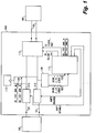
- FIG. 1 an embodiment of system in accordance with the disclosure is shown in Fig. 1 and is designated generally by reference character 100.
- the systems and methods described herein can be used for universal and/or automatic video signal detection and/or conversion for video drivers and video receivers having differing electrical or software requirements.
- a video signal termination detection system 100 includes input lines 101 configured to connect to a video driver 103 that produces a video signal.
- the system 100 can be configured as an adapter that connects separately to the video driver 103.
- the system 100 can be integrated with the video driver 103 as part of a camera or other video signal producing device, and/or integrate with a video receiver/display.
- Output lines 105 can be configured to connect to a video receiver 107 that operates with a particular signal type.
- the video receiver 107 can be configured to receive a single-ended signal, a differential signal, or any other suitable signal type.
- a single-ended signal can be configured to operate with a termination resistance of approximately 75 Ohms (e.g., 75 Ohms to a shared ground reference between the video driver and receiver) on one of the output lines 105, and the other output line 105 may be connected to ground.
- a differential signal can be configured to operate with a termination resistance on each output line 105 to ground or a higher termination resistance between the differential video signal pairs (e.g. about 100 Ohms to 1 Mega-Ohm).
- a detection circuit 109 can be connected between the input 101 and the output 105 and can be configured to detect the signal type that the video receiver 107 is capable of using (e.g. single-ended or differential).
- the detection circuit 109 can output a detection signal to a controller 111 (described in further detail below).
- a conversion circuit 113 can be configured to receive and/or filter the video signal from the video driver 103 and to convert the video signal to the required signal type if the video signal is different than the required signal type. For example, if the video signal that is output by the video driver 103 is configured for driving a single-ended termination, but the video receiver 107 requires a differential termination, the conversion circuit 113 can change the effective circuit to allow the video signal to conform to the requirements of the video receiver 107. In some embodiments, this can be accomplished by converting the effective circuit of the system 100 between a differential circuit and a single-ended circuit using one or more switches and/or by filtering as needed.
- the system 100 can also include at least one video interrupt switch 115 configured to interrupt the video signal.
- the interrupt switches 115 can include and/or be included as part of a video buffer circuit, an amplifier circuit, the detection circuit and/or any other suitable component.
- op-amp 201 is configured to act as a switch by comparing DAC NEG signal with the AMP2_DISABLE signal to output or disable a video signal when the proper disable signal is sent to the op-amp 201.
- AMP2_DISABLE can also be configured to disable the differential video reference signal when a single-ended signal is required by the receiver.
- the interrupt switch 115 can include any suitable electrical, digital, electromechanical, and/or mechanical switch (e.g. FET, MOSFET).
- the system 100 can further include a test voltage supply 117 for supplying a test voltage to the system 100 (e.g., to the receiver 107 to detect the termination of the receiver) when the video signal is interrupted by the video interrupt switch 115.
- the supplying of a test voltage can be controlled by at least one test voltage switch 119.
- the test voltage switch 119 can be any suitable electrical, digital electromechanical, and/or mechanical switch (e.g. FET, MOSFET).
- the test voltage can be any suitable voltage configured to drive the detection circuit 109 such that the detection circuit 109 can determine the required signal type for the receiver 107.
- the controller 111 as described herein can be configured to control at least one of the video interrupt switch 115, the test voltage switch 119, and the conversion circuit 113 based on a detection signal received from the detection circuit 109.
- the detection circuit 109 forms a portion of the controller 111.
- the controller 111 can include one or more processors, programmable logic, discrete logic, and/or any other suitable circuitry or device for processing signals and outputting at least one control signal.
- the controller 111 can include any necessary components to function (e.g. memory, data storage, software, firmware, etc).
- the controller 111 can be configured to automatically temporarily shut off the input video signal, switch on the test voltage, determine the receiver type, convert the effective circuit to the proper effective circuit to function with the receiver, disconnect the test voltage, and reconnect the input video signal to supply the proper video signal to the receiver.
- FIGs. 2A and 2B for a detailed embodiment of a circuit configured to act as a universal video driver - video receiver signal adapter for allowing cooperation between a single-ended signal and a differential signal mismatch.
- a controller similar to that described above is not shown in Figs. 2A and 2B , but can be included and connected to any suitable portion of system 200 (e.g. IN at SE_FLTR_EN1 in Fig. 2B ) to control any suitable component of system 200.
- a method of detecting a signal type to be received by a video receiver can include receiving a video signal, disabling the video signal from reaching the video receiver (e.g., video receiver 107), supplying a test voltage while the video signal is disabled, determining the signal type to be received by the video receiver (e.g., video receiver 107), and enabling the video signal to reach the video receiver (e.g., video receiver 107) after conforming the video signal to the signal type if the video signal is different than the signal type of the video receiver (e.g., video receiver 107).
- the disabling step can be done by disconnecting a video signal amplifier or other suitable component.
- the method can include automatically determining a signal type used by a video receiver (e.g., video receiver 107), and outputting a video signal to the video receiver (e.g., video receiver 107) in conformance with the signal type.
- a video receiver e.g., video receiver 107
- video receiver e.g., video receiver 107
- the methods and systems of the present disclosure provide for universal and/or automatic video signal detection and/or conversion systems/methods for video drivers (e.g., video driver 103) and video receivers (e.g., video receiver 107) having differing electrical and/or software requirements. While the apparatus and methods of the subject disclosure have been shown and described with reference to embodiments, those skilled in the art will readily appreciate that changes and/or modifications may be made thereto without departing from the scope of the subject disclosure as set out in the claims.
Landscapes
- Engineering & Computer Science (AREA)
- General Engineering & Computer Science (AREA)
- Theoretical Computer Science (AREA)
- Multimedia (AREA)
- Signal Processing (AREA)
- Computer Hardware Design (AREA)
- Physics & Mathematics (AREA)
- General Physics & Mathematics (AREA)
- Dc Digital Transmission (AREA)
Claims (12)
- Videosignalabschlusserkennungssystem (100), umfassend:einen Eingang (101), der konfiguriert ist, um an einen Videotreiber (103) angeschlossen zu werden, der ein Videosignal erzeugt, das einen Treibervideosignaltyp aufweist;einen Ausgang (105), der konfiguriert ist, um an einen Videoempfänger (107) angeschlossen zu werden, der mit einem Empfängervideosignaltyp betrieben wird;eine Erkennungsschaltung (109), die zwischen dem Eingang und dem Ausgang angeschlossen ist und konfiguriert ist, um den Empfängervideosignaltyp des Videoempfängers zu erkennen und um ein Erkennungssignal auszugeben;dadurch gekennzeichnet, dass das System ferner Folgendes umfasst:eine Umwandlungsschaltung (113), die konfiguriert ist, um das Videosignal von dem Videotreiber zu empfangen und um den Treibervideosignaltyp in den des Empfängers umzuwandeln, wenn sich der Treibervideosignaltyp von dem Empfängervideosignaltyp des Videoempfängers unterscheidet;einen Videounterbrechungsschalter (115; 201), der konfiguriert ist, um das Videosignal zu unterbrechen;eine Testspannungszufuhr (117) zum Zuführen einer Testspannung zu dem System, wenn das Videosignal durch den Videounterbrechungsschalter unterbrochen wird, wobei das Zuführen einer Testspannung durch zumindest einen Testspannungsschalter (119) gesteuert wird; undeine Steuerung (111), die konfiguriert ist, um zumindest eines von dem Videounterbrechungsschalter, dem Testspannungsschalter und der Umwandlungsschaltung auf Grundlage eines Erkennungssignals, das von der Erkennungsschaltung empfangen wird, zu steuern.
- Videosignalabschlusserkennungssystem nach Anspruch 1, wobei die Steuerung zumindest eines von einem Prozessor, einer diskreten Logik oder einer programmierbaren Logik beinhaltet.
- Videosignalabschlusserkennungssystem nach Anspruch 1, wobei zumindest einer von dem Videounterbrechungsschalter und dem Testspannungsschalter einen MOSFET beinhaltet, der wirkverbunden ist, um auf Grundlage eines Signals von der Steuerung ein- oder ausgeschaltet zu werden.
- Videosignalabschlusserkennungssystem nach einem der vorangehenden Ansprüche, ferner umfassend den Videotreiber.
- Videosignalabschlusserkennungssystem nach einem der vorangehenden Ansprüche, ferner umfassend den Videoempfänger.
- Videosignalabschlusserkennungssystem nach einem der vorangehenden Ansprüche, wobei der Signaltyp eines von einem asymmetrischen Videosignal und einem Differenzvideosignal ist.
- Verfahren zum Erkennung und Umwandeln eines Signaltyps, der durch einen Videoempfänger (107) empfangen werden soll, umfassend:Empfangen eines Videosignals;Deaktivieren des Videosignals, damit dieses nicht den Videoempfänger erreicht, unter Verwendung eines Videounterbrechungsschalters (115; 201), der konfiguriert ist, um das Videosignal zu unterbrechen;Zuführen einer Testspannung von einer Testspannungszufuhr (117) zu dem Videoempfänger, während das Videosignal deaktiviert wird, wobei das Zuführen einer Testspannung durch zumindest einen Testspannungsschalter (119) gesteuert wird;Bestimmen des Signaltyps, der durch den Videoempfänger empfangen werden soll, auf Grundlage eines Erkennungssignals, das von einer Erkennungsschaltung (109) empfangen wird; undAktivieren des Videosignals, damit dieses den Videoempfänger erreicht, nach Anpassen des Videosignals an den Signaltyp, wenn sich das Videosignal von dem Signaltyp des Videoempfängers unterscheidet.
- Verfahren nach Anspruch 7, wobei das Deaktivieren durch Deaktivieren eines Videosignalverstärkers durchgeführt wird.
- Verfahren nach Anspruch 7 oder 8, wobei der Signaltyp einer von einem asymmetrischen und einem Differentialtyp ist.
- Verfahren nach Anspruch 9, ferner umfassend Filtern des Videosignals nach einem einzigen Videoübertragungspfad.
- Verfahren nach einem der Ansprüche 7 bis 10, ferner umfassend Filtern eines asymmetrischen Videosignals, um durch einen Differentialabschluss verwendet werden zu können.
- Verfahren nach einem der Ansprüche 7 bis 10, ferner umfassend Filtern eines Differentialvideosignals, um durch einen asymmetrischen Abschluss verwendet werden zu können.
Applications Claiming Priority (2)
| Application Number | Priority Date | Filing Date | Title |
|---|---|---|---|
| US201461934197P | 2014-01-31 | 2014-01-31 | |
| US14/172,001 US9473710B2 (en) | 2014-01-31 | 2014-02-04 | Video signal termination detection circuit |
Publications (2)
| Publication Number | Publication Date |
|---|---|
| EP2903255A1 EP2903255A1 (de) | 2015-08-05 |
| EP2903255B1 true EP2903255B1 (de) | 2020-08-12 |
Family
ID=52434670
Family Applications (1)
| Application Number | Title | Priority Date | Filing Date |
|---|---|---|---|
| EP15153508.5A Active EP2903255B1 (de) | 2014-01-31 | 2015-02-02 | Videosignalabschlusserkennungsschaltung |
Country Status (3)
| Country | Link |
|---|---|
| US (1) | US9473710B2 (de) |
| EP (1) | EP2903255B1 (de) |
| CA (1) | CA2880057C (de) |
Families Citing this family (1)
| Publication number | Priority date | Publication date | Assignee | Title |
|---|---|---|---|---|
| JP6442836B2 (ja) * | 2014-02-28 | 2018-12-26 | セイコーエプソン株式会社 | 表示装置、および、表示装置の制御方法 |
Citations (1)
| Publication number | Priority date | Publication date | Assignee | Title |
|---|---|---|---|---|
| US6384867B1 (en) * | 1999-05-28 | 2002-05-07 | Alps Electric Co., Ltd. | Video display apparatus capable of displaying video signals of a plurality of types with different specifications |
Family Cites Families (17)
| Publication number | Priority date | Publication date | Assignee | Title |
|---|---|---|---|---|
| US5953057A (en) | 1996-09-03 | 1999-09-14 | Sensormatic Electronics Corporation | Video termination detector with data receiver |
| US6411330B1 (en) | 1998-06-10 | 2002-06-25 | Analog Devices, Inc. | Method and a circuit for detecting the presence of a television or other device on the output of a video digital to analog converter |
| JP4135229B2 (ja) * | 1998-09-29 | 2008-08-20 | ソニー株式会社 | 映像信号の変換装置および変換方法、並びにそれを使用した画像表示装置およびテレビ受信機 |
| JP2001209940A (ja) * | 1999-11-16 | 2001-08-03 | Victor Co Of Japan Ltd | 光ディスク記録再生装置、光ディスク記録再生方法および光ディスク |
| US6384637B1 (en) * | 2000-06-06 | 2002-05-07 | Rambus | Differential amplifier with selectable hysteresis and buffered filter |
| US7617513B2 (en) * | 2005-01-04 | 2009-11-10 | Avocent Huntsville Corporation | Wireless streaming media systems, devices and methods |
| JP4814547B2 (ja) | 2005-05-19 | 2011-11-16 | パナソニック株式会社 | 異常検出装置および映像システム |
| US7633560B1 (en) | 2005-08-30 | 2009-12-15 | American Megatrends, Inc. | System and apparatus for selectively terminating a video signal based on the presence or absence of a terminating device |
| KR101026397B1 (ko) * | 2006-11-16 | 2011-04-07 | 삼성전자주식회사 | 디스플레이장치 및 그 제어방법 |
| US7953162B2 (en) * | 2006-11-17 | 2011-05-31 | Intersil Americas Inc. | Use of differential pair as single-ended data paths to transport low speed data |
| JP5056211B2 (ja) * | 2007-06-29 | 2012-10-24 | ソニー株式会社 | 映像信号変換装置及び映像信号変換方法並びに映像表示装置 |
| DE102007051196B4 (de) | 2007-10-25 | 2011-12-22 | Airbus Operations Gmbh | Vorrichtung zur Bilddarstellung des Flugzeuginnenraumes |
| US7743174B2 (en) | 2007-12-28 | 2010-06-22 | Cisco Technology, Inc. | Dual utilization of a physical port of an electronic device |
| DE102010012591B4 (de) | 2010-03-23 | 2012-04-26 | Lufthansa Technik Ag | Kameraeinheit insbesondere für Überwachung in einem Transportmittel |
| CN201910228U (zh) * | 2010-11-24 | 2011-07-27 | 无锡市雷华科技有限公司 | Pci视频差分转单端卡 |
| US8410814B2 (en) * | 2011-06-16 | 2013-04-02 | Apple Inc. | Receiver circuits for differential and single-ended signals |
| CN202602805U (zh) | 2011-11-30 | 2012-12-12 | 杭州海康威视数字技术股份有限公司 | 可用双绞线传输视频信号的数字硬盘录像机及摄像机 |
-
2014
- 2014-02-04 US US14/172,001 patent/US9473710B2/en active Active
-
2015
- 2015-01-23 CA CA2880057A patent/CA2880057C/en active Active
- 2015-02-02 EP EP15153508.5A patent/EP2903255B1/de active Active
Patent Citations (1)
| Publication number | Priority date | Publication date | Assignee | Title |
|---|---|---|---|---|
| US6384867B1 (en) * | 1999-05-28 | 2002-05-07 | Alps Electric Co., Ltd. | Video display apparatus capable of displaying video signals of a plurality of types with different specifications |
Also Published As
| Publication number | Publication date |
|---|---|
| US9473710B2 (en) | 2016-10-18 |
| CA2880057A1 (en) | 2015-07-31 |
| CA2880057C (en) | 2021-06-29 |
| EP2903255A1 (de) | 2015-08-05 |
| US20150222822A1 (en) | 2015-08-06 |
Similar Documents
| Publication | Publication Date | Title |
|---|---|---|
| US20200313367A1 (en) | Semiconductor device of usb interface and method of operating the same | |
| US8207759B2 (en) | MIPI analog switch for automatic selection of multiple inputs based on clock voltages | |
| US8188764B2 (en) | Efficient electrical hibernate entry and recovery | |
| US8536733B2 (en) | Master and slave power outlet system | |
| US9772675B2 (en) | Power supply system of electronic device | |
| US10579569B2 (en) | Universal serial bus type-C interface circuit and pin bypass method thereof | |
| JP2017097688A (ja) | ポート接続回路、ポート接続制御方法、電子機器 | |
| US20120176163A1 (en) | Driving stage and related driving method | |
| US9438823B2 (en) | Signal input switching circuit, method of controlling signal input switching circuit, and display device | |
| US10289590B2 (en) | Electronic device and method of auto switching linking path giving priority to a priority port | |
| US9779049B2 (en) | Data transfer system and method of controlling the same | |
| US9473710B2 (en) | Video signal termination detection circuit | |
| US20140334112A1 (en) | Motherboard with connector compatible with different interface standards | |
| US8878590B2 (en) | Techniques for switching between AC-coupled connectivity and DC-coupled connectivity | |
| US9804986B2 (en) | Device for switching between communication modes | |
| US20140006811A1 (en) | Power supply circuit for hard disk backplane and server system using same | |
| US9509421B2 (en) | Differential signal transmission circuit, disk array controller, and differential signal transmission cable | |
| CN102693117A (zh) | 接口电路及具有接口电路的电子装置 | |
| US20140239971A1 (en) | Debugging circuit and circuit board using same | |
| JP6823729B2 (ja) | 映像機器および接続判定方法 | |
| US10362175B2 (en) | Network telephone device, external connection card and communication method therefor | |
| US20140201420A1 (en) | Transmission interface system with detection function and method | |
| US9846671B2 (en) | Bidirectional data transmission system | |
| US20120239828A1 (en) | Interface circuit and an electronic device including the same | |
| US9135199B2 (en) | System and method for signal input control and video device thereof |
Legal Events
| Date | Code | Title | Description |
|---|---|---|---|
| PUAI | Public reference made under article 153(3) epc to a published international application that has entered the european phase |
Free format text: ORIGINAL CODE: 0009012 |
|
| 17P | Request for examination filed |
Effective date: 20150202 |
|
| AK | Designated contracting states |
Kind code of ref document: A1 Designated state(s): AL AT BE BG CH CY CZ DE DK EE ES FI FR GB GR HR HU IE IS IT LI LT LU LV MC MK MT NL NO PL PT RO RS SE SI SK SM TR |
|
| AX | Request for extension of the european patent |
Extension state: BA ME |
|
| 17P | Request for examination filed |
Effective date: 20160205 |
|
| RBV | Designated contracting states (corrected) |
Designated state(s): AL AT BE BG CH CY CZ DE DK EE ES FI FR GB GR HR HU IE IS IT LI LT LU LV MC MK MT NL NO PL PT RO RS SE SI SK SM TR |
|
| STAA | Information on the status of an ep patent application or granted ep patent |
Free format text: STATUS: EXAMINATION IS IN PROGRESS |
|
| 17Q | First examination report despatched |
Effective date: 20190621 |
|
| GRAP | Despatch of communication of intention to grant a patent |
Free format text: ORIGINAL CODE: EPIDOSNIGR1 |
|
| STAA | Information on the status of an ep patent application or granted ep patent |
Free format text: STATUS: GRANT OF PATENT IS INTENDED |
|
| INTG | Intention to grant announced |
Effective date: 20200226 |
|
| RIN1 | Information on inventor provided before grant (corrected) |
Inventor name: BARTHOLOMEW, JOHN C. Inventor name: EVANS, NATHAN D. Inventor name: SWENSON, JAMES W. |
|
| GRAS | Grant fee paid |
Free format text: ORIGINAL CODE: EPIDOSNIGR3 |
|
| GRAA | (expected) grant |
Free format text: ORIGINAL CODE: 0009210 |
|
| STAA | Information on the status of an ep patent application or granted ep patent |
Free format text: STATUS: THE PATENT HAS BEEN GRANTED |
|
| AK | Designated contracting states |
Kind code of ref document: B1 Designated state(s): AL AT BE BG CH CY CZ DE DK EE ES FI FR GB GR HR HU IE IS IT LI LT LU LV MC MK MT NL NO PL PT RO RS SE SI SK SM TR |
|
| REG | Reference to a national code |
Ref country code: CH Ref legal event code: EP |
|
| REG | Reference to a national code |
Ref country code: DE Ref legal event code: R096 Ref document number: 602015057243 Country of ref document: DE |
|
| REG | Reference to a national code |
Ref country code: IE Ref legal event code: FG4D |
|
| REG | Reference to a national code |
Ref country code: AT Ref legal event code: REF Ref document number: 1302712 Country of ref document: AT Kind code of ref document: T Effective date: 20200915 |
|
| REG | Reference to a national code |
Ref country code: LT Ref legal event code: MG4D |
|
| REG | Reference to a national code |
Ref country code: NL Ref legal event code: MP Effective date: 20200812 |
|
| PG25 | Lapsed in a contracting state [announced via postgrant information from national office to epo] |
Ref country code: GR Free format text: LAPSE BECAUSE OF FAILURE TO SUBMIT A TRANSLATION OF THE DESCRIPTION OR TO PAY THE FEE WITHIN THE PRESCRIBED TIME-LIMIT Effective date: 20201113 Ref country code: FI Free format text: LAPSE BECAUSE OF FAILURE TO SUBMIT A TRANSLATION OF THE DESCRIPTION OR TO PAY THE FEE WITHIN THE PRESCRIBED TIME-LIMIT Effective date: 20200812 Ref country code: NO Free format text: LAPSE BECAUSE OF FAILURE TO SUBMIT A TRANSLATION OF THE DESCRIPTION OR TO PAY THE FEE WITHIN THE PRESCRIBED TIME-LIMIT Effective date: 20201112 Ref country code: SE Free format text: LAPSE BECAUSE OF FAILURE TO SUBMIT A TRANSLATION OF THE DESCRIPTION OR TO PAY THE FEE WITHIN THE PRESCRIBED TIME-LIMIT Effective date: 20200812 Ref country code: LT Free format text: LAPSE BECAUSE OF FAILURE TO SUBMIT A TRANSLATION OF THE DESCRIPTION OR TO PAY THE FEE WITHIN THE PRESCRIBED TIME-LIMIT Effective date: 20200812 Ref country code: ES Free format text: LAPSE BECAUSE OF FAILURE TO SUBMIT A TRANSLATION OF THE DESCRIPTION OR TO PAY THE FEE WITHIN THE PRESCRIBED TIME-LIMIT Effective date: 20200812 Ref country code: BG Free format text: LAPSE BECAUSE OF FAILURE TO SUBMIT A TRANSLATION OF THE DESCRIPTION OR TO PAY THE FEE WITHIN THE PRESCRIBED TIME-LIMIT Effective date: 20201112 Ref country code: HR Free format text: LAPSE BECAUSE OF FAILURE TO SUBMIT A TRANSLATION OF THE DESCRIPTION OR TO PAY THE FEE WITHIN THE PRESCRIBED TIME-LIMIT Effective date: 20200812 |
|
| REG | Reference to a national code |
Ref country code: AT Ref legal event code: MK05 Ref document number: 1302712 Country of ref document: AT Kind code of ref document: T Effective date: 20200812 |
|
| PG25 | Lapsed in a contracting state [announced via postgrant information from national office to epo] |
Ref country code: IS Free format text: LAPSE BECAUSE OF FAILURE TO SUBMIT A TRANSLATION OF THE DESCRIPTION OR TO PAY THE FEE WITHIN THE PRESCRIBED TIME-LIMIT Effective date: 20201212 Ref country code: PL Free format text: LAPSE BECAUSE OF FAILURE TO SUBMIT A TRANSLATION OF THE DESCRIPTION OR TO PAY THE FEE WITHIN THE PRESCRIBED TIME-LIMIT Effective date: 20200812 Ref country code: NL Free format text: LAPSE BECAUSE OF FAILURE TO SUBMIT A TRANSLATION OF THE DESCRIPTION OR TO PAY THE FEE WITHIN THE PRESCRIBED TIME-LIMIT Effective date: 20200812 Ref country code: LV Free format text: LAPSE BECAUSE OF FAILURE TO SUBMIT A TRANSLATION OF THE DESCRIPTION OR TO PAY THE FEE WITHIN THE PRESCRIBED TIME-LIMIT Effective date: 20200812 Ref country code: RS Free format text: LAPSE BECAUSE OF FAILURE TO SUBMIT A TRANSLATION OF THE DESCRIPTION OR TO PAY THE FEE WITHIN THE PRESCRIBED TIME-LIMIT Effective date: 20200812 |
|
| PG25 | Lapsed in a contracting state [announced via postgrant information from national office to epo] |
Ref country code: EE Free format text: LAPSE BECAUSE OF FAILURE TO SUBMIT A TRANSLATION OF THE DESCRIPTION OR TO PAY THE FEE WITHIN THE PRESCRIBED TIME-LIMIT Effective date: 20200812 Ref country code: RO Free format text: LAPSE BECAUSE OF FAILURE TO SUBMIT A TRANSLATION OF THE DESCRIPTION OR TO PAY THE FEE WITHIN THE PRESCRIBED TIME-LIMIT Effective date: 20200812 Ref country code: SM Free format text: LAPSE BECAUSE OF FAILURE TO SUBMIT A TRANSLATION OF THE DESCRIPTION OR TO PAY THE FEE WITHIN THE PRESCRIBED TIME-LIMIT Effective date: 20200812 Ref country code: DK Free format text: LAPSE BECAUSE OF FAILURE TO SUBMIT A TRANSLATION OF THE DESCRIPTION OR TO PAY THE FEE WITHIN THE PRESCRIBED TIME-LIMIT Effective date: 20200812 Ref country code: CZ Free format text: LAPSE BECAUSE OF FAILURE TO SUBMIT A TRANSLATION OF THE DESCRIPTION OR TO PAY THE FEE WITHIN THE PRESCRIBED TIME-LIMIT Effective date: 20200812 |
|
| REG | Reference to a national code |
Ref country code: DE Ref legal event code: R097 Ref document number: 602015057243 Country of ref document: DE |
|
| PG25 | Lapsed in a contracting state [announced via postgrant information from national office to epo] |
Ref country code: AL Free format text: LAPSE BECAUSE OF FAILURE TO SUBMIT A TRANSLATION OF THE DESCRIPTION OR TO PAY THE FEE WITHIN THE PRESCRIBED TIME-LIMIT Effective date: 20200812 Ref country code: AT Free format text: LAPSE BECAUSE OF FAILURE TO SUBMIT A TRANSLATION OF THE DESCRIPTION OR TO PAY THE FEE WITHIN THE PRESCRIBED TIME-LIMIT Effective date: 20200812 |
|
| PLBE | No opposition filed within time limit |
Free format text: ORIGINAL CODE: 0009261 |
|
| STAA | Information on the status of an ep patent application or granted ep patent |
Free format text: STATUS: NO OPPOSITION FILED WITHIN TIME LIMIT |
|
| PG25 | Lapsed in a contracting state [announced via postgrant information from national office to epo] |
Ref country code: SK Free format text: LAPSE BECAUSE OF FAILURE TO SUBMIT A TRANSLATION OF THE DESCRIPTION OR TO PAY THE FEE WITHIN THE PRESCRIBED TIME-LIMIT Effective date: 20200812 |
|
| 26N | No opposition filed |
Effective date: 20210514 |
|
| PG25 | Lapsed in a contracting state [announced via postgrant information from national office to epo] |
Ref country code: IT Free format text: LAPSE BECAUSE OF FAILURE TO SUBMIT A TRANSLATION OF THE DESCRIPTION OR TO PAY THE FEE WITHIN THE PRESCRIBED TIME-LIMIT Effective date: 20200812 |
|
| PG25 | Lapsed in a contracting state [announced via postgrant information from national office to epo] |
Ref country code: SI Free format text: LAPSE BECAUSE OF FAILURE TO SUBMIT A TRANSLATION OF THE DESCRIPTION OR TO PAY THE FEE WITHIN THE PRESCRIBED TIME-LIMIT Effective date: 20200812 |
|
| PG25 | Lapsed in a contracting state [announced via postgrant information from national office to epo] |
Ref country code: MC Free format text: LAPSE BECAUSE OF FAILURE TO SUBMIT A TRANSLATION OF THE DESCRIPTION OR TO PAY THE FEE WITHIN THE PRESCRIBED TIME-LIMIT Effective date: 20200812 |
|
| REG | Reference to a national code |
Ref country code: BE Ref legal event code: MM Effective date: 20210228 |
|
| PG25 | Lapsed in a contracting state [announced via postgrant information from national office to epo] |
Ref country code: LU Free format text: LAPSE BECAUSE OF NON-PAYMENT OF DUE FEES Effective date: 20210202 Ref country code: LI Free format text: LAPSE BECAUSE OF NON-PAYMENT OF DUE FEES Effective date: 20210228 Ref country code: CH Free format text: LAPSE BECAUSE OF NON-PAYMENT OF DUE FEES Effective date: 20210228 |
|
| PG25 | Lapsed in a contracting state [announced via postgrant information from national office to epo] |
Ref country code: IE Free format text: LAPSE BECAUSE OF NON-PAYMENT OF DUE FEES Effective date: 20210202 |
|
| PG25 | Lapsed in a contracting state [announced via postgrant information from national office to epo] |
Ref country code: BE Free format text: LAPSE BECAUSE OF NON-PAYMENT OF DUE FEES Effective date: 20210228 |
|
| REG | Reference to a national code |
Ref country code: DE Ref legal event code: R079 Ref document number: 602015057243 Country of ref document: DE Free format text: PREVIOUS MAIN CLASS: H04N0005217000 Ipc: H04N0023800000 |
|
| PG25 | Lapsed in a contracting state [announced via postgrant information from national office to epo] |
Ref country code: PT Free format text: LAPSE BECAUSE OF FAILURE TO SUBMIT A TRANSLATION OF THE DESCRIPTION OR TO PAY THE FEE WITHIN THE PRESCRIBED TIME-LIMIT Effective date: 20201214 |
|
| PG25 | Lapsed in a contracting state [announced via postgrant information from national office to epo] |
Ref country code: HU Free format text: LAPSE BECAUSE OF FAILURE TO SUBMIT A TRANSLATION OF THE DESCRIPTION OR TO PAY THE FEE WITHIN THE PRESCRIBED TIME-LIMIT; INVALID AB INITIO Effective date: 20150202 |
|
| PG25 | Lapsed in a contracting state [announced via postgrant information from national office to epo] |
Ref country code: CY Free format text: LAPSE BECAUSE OF FAILURE TO SUBMIT A TRANSLATION OF THE DESCRIPTION OR TO PAY THE FEE WITHIN THE PRESCRIBED TIME-LIMIT Effective date: 20200812 |
|
| PG25 | Lapsed in a contracting state [announced via postgrant information from national office to epo] |
Ref country code: MK Free format text: LAPSE BECAUSE OF FAILURE TO SUBMIT A TRANSLATION OF THE DESCRIPTION OR TO PAY THE FEE WITHIN THE PRESCRIBED TIME-LIMIT Effective date: 20200812 |
|
| PG25 | Lapsed in a contracting state [announced via postgrant information from national office to epo] |
Ref country code: MT Free format text: LAPSE BECAUSE OF FAILURE TO SUBMIT A TRANSLATION OF THE DESCRIPTION OR TO PAY THE FEE WITHIN THE PRESCRIBED TIME-LIMIT Effective date: 20200812 |
|
| PG25 | Lapsed in a contracting state [announced via postgrant information from national office to epo] |
Ref country code: TR Free format text: LAPSE BECAUSE OF FAILURE TO SUBMIT A TRANSLATION OF THE DESCRIPTION OR TO PAY THE FEE WITHIN THE PRESCRIBED TIME-LIMIT Effective date: 20200812 |
|
| P01 | Opt-out of the competence of the unified patent court (upc) registered |
Free format text: CASE NUMBER: UPC_APP_0016738_2903255/2025 Effective date: 20251210 |
|
| PGFP | Annual fee paid to national office [announced via postgrant information from national office to epo] |
Ref country code: GB Payment date: 20260121 Year of fee payment: 12 |
|
| PGFP | Annual fee paid to national office [announced via postgrant information from national office to epo] |
Ref country code: DE Payment date: 20260121 Year of fee payment: 12 |
|
| PGFP | Annual fee paid to national office [announced via postgrant information from national office to epo] |
Ref country code: FR Payment date: 20260121 Year of fee payment: 12 |