EP2901211B1 - Illumination devices using array of reflectors - Google Patents
Illumination devices using array of reflectors Download PDFInfo
- Publication number
- EP2901211B1 EP2901211B1 EP13776983.2A EP13776983A EP2901211B1 EP 2901211 B1 EP2901211 B1 EP 2901211B1 EP 13776983 A EP13776983 A EP 13776983A EP 2901211 B1 EP2901211 B1 EP 2901211B1
- Authority
- EP
- European Patent Office
- Prior art keywords
- light sources
- light
- reflector
- plate
- optical system
- Prior art date
- Legal status (The legal status is an assumption and is not a legal conclusion. Google has not performed a legal analysis and makes no representation as to the accuracy of the status listed.)
- Active
Links
Images





Classifications
-
- F—MECHANICAL ENGINEERING; LIGHTING; HEATING; WEAPONS; BLASTING
- F21—LIGHTING
- F21V—FUNCTIONAL FEATURES OR DETAILS OF LIGHTING DEVICES OR SYSTEMS THEREOF; STRUCTURAL COMBINATIONS OF LIGHTING DEVICES WITH OTHER ARTICLES, NOT OTHERWISE PROVIDED FOR
- F21V7/00—Reflectors for light sources
- F21V7/0083—Array of reflectors for a cluster of light sources, e.g. arrangement of multiple light sources in one plane
-
- G—PHYSICS
- G03—PHOTOGRAPHY; CINEMATOGRAPHY; ANALOGOUS TECHNIQUES USING WAVES OTHER THAN OPTICAL WAVES; ELECTROGRAPHY; HOLOGRAPHY
- G03B—APPARATUS OR ARRANGEMENTS FOR TAKING PHOTOGRAPHS OR FOR PROJECTING OR VIEWING THEM; APPARATUS OR ARRANGEMENTS EMPLOYING ANALOGOUS TECHNIQUES USING WAVES OTHER THAN OPTICAL WAVES; ACCESSORIES THEREFOR
- G03B21/00—Projectors or projection-type viewers; Accessories therefor
- G03B21/14—Details
- G03B21/20—Lamp housings
- G03B21/2006—Lamp housings characterised by the light source
- G03B21/2013—Plural light sources
-
- G—PHYSICS
- G02—OPTICS
- G02B—OPTICAL ELEMENTS, SYSTEMS OR APPARATUS
- G02B17/00—Systems with reflecting surfaces, with or without refracting elements
- G02B17/006—Systems in which light light is reflected on a plurality of parallel surfaces, e.g. louvre mirrors, total internal reflection [TIR] lenses
-
- G—PHYSICS
- G03—PHOTOGRAPHY; CINEMATOGRAPHY; ANALOGOUS TECHNIQUES USING WAVES OTHER THAN OPTICAL WAVES; ELECTROGRAPHY; HOLOGRAPHY
- G03B—APPARATUS OR ARRANGEMENTS FOR TAKING PHOTOGRAPHS OR FOR PROJECTING OR VIEWING THEM; APPARATUS OR ARRANGEMENTS EMPLOYING ANALOGOUS TECHNIQUES USING WAVES OTHER THAN OPTICAL WAVES; ACCESSORIES THEREFOR
- G03B21/00—Projectors or projection-type viewers; Accessories therefor
- G03B21/14—Details
- G03B21/20—Lamp housings
- G03B21/2006—Lamp housings characterised by the light source
- G03B21/2033—LED or laser light sources
-
- G—PHYSICS
- G03—PHOTOGRAPHY; CINEMATOGRAPHY; ANALOGOUS TECHNIQUES USING WAVES OTHER THAN OPTICAL WAVES; ELECTROGRAPHY; HOLOGRAPHY
- G03B—APPARATUS OR ARRANGEMENTS FOR TAKING PHOTOGRAPHS OR FOR PROJECTING OR VIEWING THEM; APPARATUS OR ARRANGEMENTS EMPLOYING ANALOGOUS TECHNIQUES USING WAVES OTHER THAN OPTICAL WAVES; ACCESSORIES THEREFOR
- G03B21/00—Projectors or projection-type viewers; Accessories therefor
- G03B21/14—Details
- G03B21/20—Lamp housings
- G03B21/2066—Reflectors in illumination beam
Definitions
- High-wattage Xenon lamps are often used in projectors for digital cinema, large venues, and for fixed installations. Such projectors typically use Xenon lamps with wattage range of 2-6 kW and have brightness in the range of 10,000-30,000 lumens. High-wattage Xenon lamps have relatively short lifetime, typically in the range of 500-1000 hours.
- UHP Mercury arc lamps are often used in compact and portable projectors for home or office use. Such projectors typically use UHP Mercury arc lamps with wattage range of 120-350 W and have brightness in the range of 1000-5000 lumens. UHP Mercury arc lamps have a typical lifetime of about 2000 hours, which is still relatively short.
- US2012/133903 discloses a light source device including a first and second solid-state light source units disposed opposite to each other, each unit including solid-state light sources; a reflection unit; a condensing part; and a fluorescence emission plate excited with a condensed light beam.
- the light sources in each of the units are arranged two-dimensionally with the optical axes oriented in an x-axis direction.
- Each column of the light sources of the first and the second light source units are arranged alternately in the y-axis direction.
- the reflection unit reflects the light beams from the light source units in the z-axis direction so as to be arranged into a two-dimensional array in a xy plane.
- a density of the reflected light beams in the x-axis direction is higher than that of the arrangement of the light sources in the z-axis direction.
- Light from solid-state light sources are condensed and combined efficiently, with a compact configuration.
- US2009/153752 discloses a digital image projector for increasing brightness includes a first light source; a second light source that is spectrally adjacent to the first light source; a dichroic beamsplitter disposed to direct light of both the first and second light source; a spatial light modulator that receives light from both the first and second light sources; and projection optics for delivering imaging light from the spatial light modulator.
- EP1538832 discloses light path changing members and each light path changing member 2 forms a first light flux by reflecting a half of light flux emitted from a particular area (central area or peripheral area) of light source 1A in one direction using a polarizing beam splitter 20, and forms a second light flux by reflecting the other half of light flux, which has passed through the beam splitter, in the afore-mentioned direction using the first mirror 21.
- each light path changing member transmits a half of a light flux emitted from the other light source 1B and guided by the second mirror 22 in the same direction as that in which the first light flux has been guided using the polarizing beam splitter 20, and superposes the light flux on the aforementioned first light flux, and reflects the other half of light flux, which has been reflected by the beam splitter 20,in the aforementioned direction using the first mirror 21, and superposes the light flux on the second light flux.
- JP2011043703 is said to provide an illuminator capable of yielding bright illuminating light with excellent illumination efficiency.
- the illuminator 10A includes a plurality of laser array light sources 11 having a plurality of semiconductor laser elements 11b emitting a laser beam L having nearly single wavelength in a line in a column direction and installed along the column direction of the plurality of semiconductor laser elements 11b, and a dichroic mirror 12DM (or a total reflection mirror 12M) having a plurality of rectangular mirror parts 12a and 12b corresponding to the number of the plurality of laser array light sources 11 and installed in a state where the plurality of rectangular mirror parts 12a and 12b are orthogonally superposed alternately in a row direction perpendicular to the column direction of the laser array light source 11.
- the illuminator 10A is constituted by opposing the plurality of laser array light sources 11 to positionally differ in the row direction and alternately separate while putting the dichroic mirror 12DM (or the total reflection mirror 12M) in between.
- Embodiments of the present invention provide apparatuses and systems for providing illumination for projectors.
- Two or more sets of reflectors are used to combine light beams emitted by two or more two-dimensional arrays of light sources to provide a combined light beam with high brightness toward a pupil of a projection system.
- Solid state light sources such as diode lasers and LEDs, may be used as light sources at relatively low cost and low powers, and with long lifetime.
- Claim 1 relates to an optical system for providing illumination to a pupil of an imaging device.
- the optical system comprises a first two-dimensional array of first light sources disposed in rows and columns, and a second two-dimensional array of second light sources disposed in rows and columns.
- the second light sources are interleaved with the first light sources in both the column direction and the row direction.
- the optical system further comprises a first set of first reflectors and a second set of second reflectors.
- the first set of first reflectors is disposed as a staggered array such that each first reflector is operable to reflect first light beams provided by a respective row of first light sources toward the pupil of the imaging device.
- the second set of second reflectors is disposed as a staggered array such that each second reflector is operable to reflect second light beams provided by a respective row of second light sources toward the pupil of the imaging device.
- Each second reflector is stacked in front of a corresponding first reflector in the direction toward the pupil and comprises transparent regions operable to transmit the first light beams reflected by a corresponding first reflector.
- Claims 12 and 13 relate to optical devices.
- Embodiments of the present invention can provide apparatuses and systems for providing illumination for projectors with suitable brightness using lasers or other long lifetime light sources. For example, two or more sets of reflectors are used to combine light beams emitted by two or more two-dimensional arrays of light sources to provide a combined light beam with high brightness toward a pupil of a projection system. Solid state light sources, such as diode lasers and LEDs, may be used as light sources at relatively low cost and low power, and with long lifetime.
- FIG. 1 is a cross sectional view of a simplified schematic diagram of a projection system 100 that may utilize embodiments of the present invention.
- Light 102 (represented by a thick arrow) provided by an illumination device 104 proceeds through a condenser lens 110 and a total internal reflection (TIR) prism 130, and is focused onto an imager 120, where the light rays are converted into video information.
- the imager 120 may comprise, for example, a digital micromirror device (DMD), a liquid crystal light valve, or the like, which modulates the amplitude of the light rays in various spatial regions corresponding to various pixels of an image.
- the modulated light rays then pass through a projection lens 140 to form an enlarged image at a display device 150.
- the display device 150 may comprise, for example, a wall, a screen, or the like.
- Embodiments of the present invention provide illumination devices for providing illumination to projection systems, such as the one shown in FIG. 1 .
- FIG. 2A is a partial perspective view of a simplified schematic diagram of an optical system 200 according to an embodiment of the invention.
- the optical system 200 includes a first two-dimensional array 210 of light sources, a second two-dimensional array 220 of light sources, a set of first reflectors 250, and a set of second reflectors 260.
- the first two-dimensional array 210 of light sources comprises a plurality of first light sources 212 disposed on a first plate 214.
- the second two-dimensional array 220 of light sources comprises a plurality of second light sources 222 disposed on a second plate 224.
- FIG. 2B is a cross sectional view of a simplified schematic diagram of the optical system 200 shown in FIG. 2A , along with schematic ray diagrams.
- each first light source 212 is operable to emit a first light beam 202 (denoted by a dotted line) in a direction (e.g., the +x direction) perpendicular to the first plate 214.
- Each second light source 222 is operable to emit a second light beam 204 (denoted by a thin solid line) in a direction (e.g., the +x direction) perpendicular to the second plate 224.
- each first light source 212 or second light source 222 comprises a solid state light-emitting device, such as a diode laser, an LED, or the like.
- Each first light source 212 or second light source 222 may be operable to provide a collimated light beam or non-collimated light beam according to various embodiments.
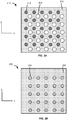
- FIG. 3A is a plan view of a simplified schematic diagram of the first two-dimensional array 210 of light sources according to an embodiment of the invention.
- the first two-dimensional array 210 of light sources comprises a plurality of rows formed of first light sources 212 disposed in a row direction (e.g., the y direction, which is perpendicular to the paper of FIG. 2B ), and a plurality of columns formed of first light sources 212 disposed in a column direction (e.g., the z direction).
- the first two-dimensional array of light sources is disposed on the first plate 214.
- the first plate 214 comprises an array of transparent regions 216.
- the transparent regions 216 are interleaved with the first light sources 212 in both the row direction and the column direction.
- Each transparent region 216 may comprise a hole or a transparent material.
- FIG. 3B is a plan view of a simplified schematic diagram of the second two-dimensional array 220 of light sources according to an embodiment of the invention.
- the second two-dimensional array 220 of light sources comprises a plurality of rows formed of second light sources 222 disposed in a row direction (e.g., the y direction), and a plurality of columns formed of second light sources 222 disposed in a column direction (e.g., the z direction).
- the second two-dimensional array 220 of light sources is disposed on the second plate 224 in the same spatial pattern as that of the array of transparent regions 216 on the first plate 214.
- the second two-dimensional array 220 of light sources is positioned behind the first two-dimensional array 210 of light sources in the +x direction.
- the first plate 214 and the second plate 224 are properly aligned with respect to each other, so that the second light sources 222 on the second plate 224 are directly behind the transparent regions 216 on the first plate 214 in the +x direction.
- the transparent regions 216 in the first plate 214 are operable to transmit the second light beams 204 emitted by the second light sources 222.
- the set of first reflectors 250a-e is disposed as an array in the x direction and is staggered in the z direction, such that the z coordinate of each first reflector 250 is approximately the same as that of a corresponding row of first light sources 212.
- FIG. 4A is a plan view of a simplified schematic diagram of a first reflector 250 according to an embodiment of the invention.
- the first reflector 250 comprises a reflective surface 256 in the shape of a rectangle elongated in the y direction (which is perpendicular to the paper of FIG. 2B ). It should be appreciated that the reflective surface 256 of the first reflector 250 may be characterized by other shapes in some embodiments.
- the first reflector 250 comprises a thin metal strip.
- the first reflector 250 comprises a dielectric plate or prism, with the reflective surface 256 being metallized with visible-light enhanced aluminum deposition, cold-mirror deposition, or other types of high-reflection coating suitable for the purposes.
- each first reflector 250 is positioned such that a normal of the reflective surface 256 of each first reflector 250 is in the x-z plane and is tilted at an angle with respect to the x direction.
- each first reflector 250 is operable to reflect the first light beams 202 emitted by a respective row of first light sources 212 into a direction (e.g., the -z direction) toward a pupil 290 of an imaging device.
- the shaded oval circles 252 in FIG. 4A indicate the footprints of the first light beams 202 emitted by a row of first light sources 212 when the first light beams 202 imping upon a corresponding first reflector 250.
- the angle between the normal of the reflective surface 256 of each first reflector 250 and the x-axis is approximately 45 degrees. In this case, the first light beams 202 are incident on each first reflector at approximately 45-degree angle of incidence. In other embodiments, the angle between the normal of the reflective surface 256 of each first reflector 250 and the x-axis is different from 45 degrees.
- the set of second reflectors 260a-e is also disposed as an array in the x direction.
- the set of second reflectors 260a-e is staggered and disposed in front of the set of first reflectors 250a-e in the z direction, such that z coordinate of each second reflector 260 is approximately the same as that of a corresponding row of second light sources 222.
- FIG. 4B is a plan view of a simplified schematic diagram of a second reflector 260 according to an embodiment of the invention.
- the second reflector 260 comprises a reflective surface 266 in the shape of a rectangle elongated in the y direction (which is perpendicular to the paper of FIG. 2B ). It should be appreciated that the reflective surface 266 of the second reflector 260 may be characterized by other shapes in some embodiments.
- the second reflector 260 comprises a thin metal strip.
- the second reflector 260 comprises a dielectric plate or prism, with the reflective surface 266 being metallized with visible-light enhanced aluminum deposition, cold-mirror deposition, or other types of high-reflection coating suitable for the purposes.
- each second reflector 260 is positioned such that a normal of the reflective surface 266 of each second reflector 260 is in the x-z plane and is tilted at an angle with respect to the x direction.
- each second reflector 260 is operable to reflect the second light beams 204 emitted by a respective row of second light sources 222 into a direction (e.g., the -z direction) toward the pupil 290 of the imaging device.
- the hatched oval circles 262 in FIG. 4B indicate the footprints of the second light beams 204 emitted by a row of second light sources 222 when the second light beams 204 impinge upon a corresponding second reflector 260.
- the angle between the normal of the reflective surface 266 of each second reflector 260 and the x direction is approximately 45 degrees.
- the second light beams 204 are incident on each second reflector 260 at approximately 45-degree angle of incidence.
- the angle between the normal of the reflective surface 266 of each second reflector 260 and the x direction is different from 45 degrees.
- the second reflector 260 comprises a plurality of transparent regions 264 disposed as an array in the y direction (which is perpendicular to the paper of FIG. 2B ) in the spaces between adjacent footprints 262 of the second light beams 204.
- Each transparent region 264 may comprise a hole or a transparent material.
- the set of first reflectors 250 and the set of second reflectors 260 are operable to combine the first light beams 202 emitted by the first light sources 212 and the second light beams 204 emitted by the second light sources into a combined light beam in the direction (e.g., the -z direction) toward the pupil 290.
- FIG. 5A is a plan view of a pupil 290 of an imaging device when it is illuminated by the combined light beam provided by the optical system 200, according to an embodiment of the invention.
- the shaded circles 292 indicate the footprints of the first light beams 202 emitted by the first light sources 212 when they impinge on the pupil 290.
- the hatched circles 294 indicate the footprints of the second light beams 204 emitted by the second light sources 222 when they impinge on the pupil 290. It can be seen that, the first light beams 202 emitted by each row of first light sources 212 and the second light beams 204 emitted by a corresponding row of second light sources 222 are mapped into a single column of light beams (in the y direction in FIG.
- adjacent columns of light beams in the combined light beam are closely spaced with respect to each other, such that the first light beams 202 and the second light beams 204 are compressed into a combined light beam that fills only half side of the pupil 290.
- the optical system 200 affords several advantages.
- First, the first light sources 212 and the second light sources 222 may be arranged on the first plate 214 and the second plate 224, respectively, with relatively large spacings between adjacent rows and columns, while still achieving a compact combined light beam. A relatively sparse arrangement of the light sources on each plate would allow better heat dissipation, thereby improving performance.
- the optical system 200 further comprises a third two-dimensional array 230 of light sources, a fourth two-dimensional array 240 of light sources, a set of third reflectors 270, and a set of fourth reflectors 280.
- the set of third reflectors 270 and the set of fourth reflectors 280 are mirror images of the set of first reflectors 250 and the set of second reflectors 260, respectively, with respect to a y-z plane 205 (which is perpendicular to the paper of FIG. 2B ) that intersects the pupil 290 at approximately a middle line thereof.
- the third two-dimensional array 230 of light sources and the fourth two-dimensional array 240 of light sources are mirror images of the first two-dimensional array 210 of light sources and the second two-dimensional array 220 of light sources, respectively, with respect to the same y-z plane 205.
- the set of third reflectors 270 and the set of fourth reflectors 280 are operable to combine the light beams emitted by the third two-dimensional array 230 of light sources and the fourth two-dimensional array 240 of light sources to form a second combined light beam that would fill the other half side of the pupil 290, as shown in FIG. 5B .
- the optical system 200 may be viewed as comprising two sub-devices that are mirror images of each other: a first sub-device comprising the first two-dimensional array 210 of light sources, the second two-dimensional array 220 of light sources, the set of first reflectors 250, and the set of second reflectors 260, and a second sub-device comprising the third two-dimensional array 230 of light sources, the fourth two-dimensional array 240 of light sources, the set of third reflectors 270, and the set of fourth reflectors 280.
- the optical system 200 may be used to provides a scalable illumination device for a projection system.
- Such an illumination device is scalable in the sense that higher brightness may be achieved by increasing the number of light sources in each of the four arrays 210, 220, 230, and 240 of light sources. Therefore, a high-brightness illumination device may be achieved.
- Such an illumination device has the advantage that four arrays 210, 220, 230, and 240 of light sources mounted on four separate plates are used to provide a combined light beam toward a pupil of an imaging device. As such, the heat load on each plate may be more manageable compared to the case where all light sources are mounted on a single plate. Furthermore, as discussed above, a more compact combined light beam may be achieved than what could be achievable otherwise.
- each of the four arrays 210, 220, 230, and 240 of light sources may be configured such that an outer periphery of the footprints of the combined light beam matches closely to the shape of the pupil 290, as illustrated in the example shown in FIG. 5C .
- the four arrays 210, 220, 230, and 240 of light sources are configured such that the outer periphery the footprints of the combined light beam matches closely the circular shape of the pupil 290. In this manner, the potential waste of light that may fall outside the pupil 290 is avoided. Conversely, under-filling of the pupil 290 may also be avoided.
- the four arrays 210, 220, 230, and 240 of light sources may be configured for other pupil shapes, such as square, rectangle, triangle, and the like.
- FIG. 6 is a cross sectional view of a simplified schematic diagram of an optical system 600, along with schematic ray diagrams, according to another embodiment of the invention.
- the optical system 600 is similar to the optical system 200 shown in FIGS. 2A and 2B , except that the first array of first light sources 612 and the second array of second light sources 622 are mounted on the same plate 614 as a first illumination source 610. Similarly, the third array of third light sources 632 and the fourth array of fourth light sources 642 are mounted on the same plate 634 as a second illumination source 630.
- the optical system also comprises a set of first reflectors 650, a set of second reflectors 660, a set of third reflectors 670, and a set of fourth reflectors 680, arranged in the same manner as in the optical system 200 shown in FIGS. 2A and 2B .
- FIG. 7 is a plan view of a simplified schematic diagram of an illumination source 700 according to an embodiment of the invention, which may be used as the first illumination source 610 and the second illumination source 630.
- the illumination source 700 comprises a first array of first light sources 612 (represented by the dark shaded circles) disposed in rows and columns.
- the illumination source 700 also comprises a second array of second light sources 622 (represented by the hatched circles) disposed in rows and columns.
- the first light sources 612 are interleaved with the second light sources 622 in both the row direction (e.g., the y direction) and the column direction (e.g., the z direction).
- the set of first reflectors 650, the set of the second reflectors 660, the set of third reflectors 670, and the set of fourth reflectors 680 are operable to combine the first light beams 602, the second light beams 604, the third light beams 606, and the fourth light beams 608 emitted by the first light sources 612, the second light sources 622, the third light sources 632, and the fourth light sources 642, respectively, to form a combined light beam toward a pupil 690 of an imaging device.
- the optical system 600 can be less complex.
- the first array of first light sources 612 and the second array of second light sources 622 (or the array of third light sources 632 and the array of fourth light sources 642) are mounted on a single plate instead of two separate plates, no alignment between two plates is necessary. However, the simplicity is achieved at the expense of having higher heat load on the single plate.
- the first light sources 612 and the second light sources 622 are interleaved on a single plate, the spacings between adjacent light sources are smaller compared to the case in the optical system 200 where the first light sources 212 and the second light sources 222 are mounted on two separate plates as shown in FIGS. 3A and 3B . Since each light source may have fixtures that occupy a peripheral area around the light-emitting area of the light source, there may be a physical limit as how compact the light sources can be arranged on the plate.
Landscapes
- Physics & Mathematics (AREA)
- General Physics & Mathematics (AREA)
- Optics & Photonics (AREA)
- Engineering & Computer Science (AREA)
- General Engineering & Computer Science (AREA)
- Non-Portable Lighting Devices Or Systems Thereof (AREA)
- Projection Apparatus (AREA)
Description
- Most high brightness projectors available now use either Xenon lamps or ultra high performance (UHP) Mercury arc lamps. High-wattage Xenon lamps are often used in projectors for digital cinema, large venues, and for fixed installations. Such projectors typically use Xenon lamps with wattage range of 2-6 kW and have brightness in the range of 10,000-30,000 lumens. High-wattage Xenon lamps have relatively short lifetime, typically in the range of 500-1000 hours. UHP Mercury arc lamps are often used in compact and portable projectors for home or office use. Such projectors typically use UHP Mercury arc lamps with wattage range of 120-350 W and have brightness in the range of 1000-5000 lumens. UHP Mercury arc lamps have a typical lifetime of about 2000 hours, which is still relatively short.
- Therefore, it is desirable to have projectors that utilize light sources with much longer lifetimes while still providing suitable brightness.
-
US2012/133903 discloses a light source device including a first and second solid-state light source units disposed opposite to each other, each unit including solid-state light sources; a reflection unit; a condensing part; and a fluorescence emission plate excited with a condensed light beam. The light sources in each of the units are arranged two-dimensionally with the optical axes oriented in an x-axis direction. Each column of the light sources of the first and the second light source units are arranged alternately in the y-axis direction. The reflection unit reflects the light beams from the light source units in the z-axis direction so as to be arranged into a two-dimensional array in a xy plane. A density of the reflected light beams in the x-axis direction is higher than that of the arrangement of the light sources in the z-axis direction. Light from solid-state light sources are condensed and combined efficiently, with a compact configuration. -
US2009/153752 discloses a digital image projector for increasing brightness includes a first light source; a second light source that is spectrally adjacent to the first light source; a dichroic beamsplitter disposed to direct light of both the first and second light source; a spatial light modulator that receives light from both the first and second light sources; and projection optics for delivering imaging light from the spatial light modulator. -
EP1538832 discloses light path changing members and each light path changing member 2 forms a first light flux by reflecting a half of light flux emitted from a particular area (central area or peripheral area) of light source 1A in one direction using a polarizing beam splitter 20, and forms a second light flux by reflecting the other half of light flux, which has passed through the beam splitter, in the afore-mentioned direction using the first mirror 21. Then, each light path changing member transmits a half of a light flux emitted from the other light source 1B and guided by the second mirror 22 in the same direction as that in which the first light flux has been guided using the polarizing beam splitter 20, and superposes the light flux on the aforementioned first light flux, and reflects the other half of light flux, which has been reflected by the beam splitter 20,in the aforementioned direction using the first mirror 21, and superposes the light flux on the second light flux. -
JP2011043703 - Embodiments of the present invention provide apparatuses and systems for providing illumination for projectors. Two or more sets of reflectors are used to combine light beams emitted by two or more two-dimensional arrays of light sources to provide a combined light beam with high brightness toward a pupil of a projection system. Solid state light sources, such as diode lasers and LEDs, may be used as light sources at relatively low cost and low powers, and with long lifetime.
- Claim 1 relates to an optical system for providing illumination to a pupil of an imaging device is provided. The optical system comprises a first two-dimensional array of first light sources disposed in rows and columns, and a second two-dimensional array of second light sources disposed in rows and columns. The second light sources are interleaved with the first light sources in both the column direction and the row direction. The optical system further comprises a first set of first reflectors and a second set of second reflectors. The first set of first reflectors is disposed as a staggered array such that each first reflector is operable to reflect first light beams provided by a respective row of first light sources toward the pupil of the imaging device. The second set of second reflectors is disposed as a staggered array such that each second reflector is operable to reflect second light beams provided by a respective row of second light sources toward the pupil of the imaging device. Each second reflector is stacked in front of a corresponding first reflector in the direction toward the pupil and comprises transparent regions operable to transmit the first light beams reflected by a corresponding first reflector.
- Claims 12 and 13 relate to optical devices.
-
-
FIG. 1 is a cross sectional view of a simplified schematic diagram of a projection system; -
FIG. 2A is a partial perspective view of a simplified schematic diagram of an optical system according to an embodiment of the invention; -
FIG. 2B is a cross sectional view of a simplified schematic diagram of the optical system shown inFIG. 2A , along with schematic ray diagrams; -
FIG. 3A is a plan view of a simplified schematic diagram of a two-dimensional array of light sources usable in the optical system shown inFIGS. 2A and2B , according to an embodiment of the invention; -
FIG. 3B is a plan view of a simplified schematic diagram of another two-dimensional array of light sources usable in the optical system shown inFIGS. 2A and2B , according to an embodiment of the invention;FIG. 4A is a plan view of a simplified schematic diagram of a reflector usable in the optical system shown inFIGS. 2A and2B , according to an embodiment of the invention; -
FIG. 4B a plan view of a simplified schematic diagram of another reflector usable in the optical system shown inFIGS. 2A and2B , according to an embodiment of the invention; -
FIG. 5A is a plan view of a pupil of an imaging device according to an embodiment of the invention; -
FIG. 5B is a plan view of a pupil of an imaging device according to another embodiment of the invention; -
FIG. 5C is a plan view of a pupil of an imaging device according to a further embodiment of the invention; -
FIG. 6 is a cross sectional view of a simplified schematic diagram of an optical system, along with schematic ray diagrams, according to another embodiment of the invention; and -
FIG. 7 is a plan view of a simplified schematic diagram of an illumination source usable in the optical system shown inFIG. 6 , according to an embodiment of the invention. - Most high brightness projectors available now use either Xenon lamps or UHP Mercury arc lamps. High-wattage Xenon lamps and UHP Mercury arc lamps, however, have relatively short lifetime. Therefore, it is desirable to have projectors that utilize light sources with much longer lifetimes while still providing suitable brightness. Embodiments of the present invention can provide apparatuses and systems for providing illumination for projectors with suitable brightness using lasers or other long lifetime light sources. For example, two or more sets of reflectors are used to combine light beams emitted by two or more two-dimensional arrays of light sources to provide a combined light beam with high brightness toward a pupil of a projection system. Solid state light sources, such as diode lasers and LEDs, may be used as light sources at relatively low cost and low power, and with long lifetime.
-
FIG. 1 is a cross sectional view of a simplified schematic diagram of aprojection system 100 that may utilize embodiments of the present invention. Light 102 (represented by a thick arrow) provided by anillumination device 104 proceeds through acondenser lens 110 and a total internal reflection (TIR)prism 130, and is focused onto animager 120, where the light rays are converted into video information. Theimager 120 may comprise, for example, a digital micromirror device (DMD), a liquid crystal light valve, or the like, which modulates the amplitude of the light rays in various spatial regions corresponding to various pixels of an image. The modulated light rays then pass through aprojection lens 140 to form an enlarged image at adisplay device 150. Thedisplay device 150 may comprise, for example, a wall, a screen, or the like. Embodiments of the present invention, as will be described in more detail below, provide illumination devices for providing illumination to projection systems, such as the one shown inFIG. 1 . -
FIG. 2A is a partial perspective view of a simplified schematic diagram of anoptical system 200 according to an embodiment of the invention. Theoptical system 200 includes a first two-dimensional array 210 of light sources, a second two-dimensional array 220 of light sources, a set offirst reflectors 250, and a set ofsecond reflectors 260. The first two-dimensional array 210 of light sources comprises a plurality of firstlight sources 212 disposed on afirst plate 214. The second two-dimensional array 220 of light sources comprises a plurality of secondlight sources 222 disposed on asecond plate 224. -
FIG. 2B is a cross sectional view of a simplified schematic diagram of theoptical system 200 shown inFIG. 2A , along with schematic ray diagrams. As shown, eachfirst light source 212 is operable to emit a first light beam 202 (denoted by a dotted line) in a direction (e.g., the +x direction) perpendicular to thefirst plate 214. Each secondlight source 222 is operable to emit a second light beam 204 (denoted by a thin solid line) in a direction (e.g., the +x direction) perpendicular to thesecond plate 224. In one embodiment, eachfirst light source 212 or secondlight source 222 comprises a solid state light-emitting device, such as a diode laser, an LED, or the like. Each firstlight source 212 or secondlight source 222 may be operable to provide a collimated light beam or non-collimated light beam according to various embodiments. -
FIG. 3A is a plan view of a simplified schematic diagram of the first two-dimensional array 210 of light sources according to an embodiment of the invention. The first two-dimensional array 210 of light sources comprises a plurality of rows formed of firstlight sources 212 disposed in a row direction (e.g., the y direction, which is perpendicular to the paper ofFIG. 2B ), and a plurality of columns formed of firstlight sources 212 disposed in a column direction (e.g., the z direction). The first two-dimensional array of light sources is disposed on thefirst plate 214. - As shown in
FIG. 3A , thefirst plate 214 comprises an array oftransparent regions 216. Thetransparent regions 216 are interleaved with thefirst light sources 212 in both the row direction and the column direction. Eachtransparent region 216 may comprise a hole or a transparent material. -
FIG. 3B is a plan view of a simplified schematic diagram of the second two-dimensional array 220 of light sources according to an embodiment of the invention. The second two-dimensional array 220 of light sources comprises a plurality of rows formed of secondlight sources 222 disposed in a row direction (e.g., the y direction), and a plurality of columns formed of secondlight sources 222 disposed in a column direction (e.g., the z direction). The second two-dimensional array 220 of light sources is disposed on thesecond plate 224 in the same spatial pattern as that of the array oftransparent regions 216 on thefirst plate 214. - As shown in
FIG. 2B , the second two-dimensional array 220 of light sources is positioned behind the first two-dimensional array 210 of light sources in the +x direction. Thefirst plate 214 and thesecond plate 224 are properly aligned with respect to each other, so that the secondlight sources 222 on thesecond plate 224 are directly behind thetransparent regions 216 on thefirst plate 214 in the +x direction. In this manner, thetransparent regions 216 in thefirst plate 214 are operable to transmit the secondlight beams 204 emitted by the secondlight sources 222. - As shown in
FIG. 2B , the set offirst reflectors 250a-e is disposed as an array in the x direction and is staggered in the z direction, such that the z coordinate of eachfirst reflector 250 is approximately the same as that of a corresponding row of firstlight sources 212. -
FIG. 4A is a plan view of a simplified schematic diagram of afirst reflector 250 according to an embodiment of the invention. Thefirst reflector 250 comprises areflective surface 256 in the shape of a rectangle elongated in the y direction (which is perpendicular to the paper ofFIG. 2B ). It should be appreciated that thereflective surface 256 of thefirst reflector 250 may be characterized by other shapes in some embodiments. In one embodiment, thefirst reflector 250 comprises a thin metal strip. In other embodiments, thefirst reflector 250 comprises a dielectric plate or prism, with thereflective surface 256 being metallized with visible-light enhanced aluminum deposition, cold-mirror deposition, or other types of high-reflection coating suitable for the purposes. - As shown in
FIG. 2B , eachfirst reflector 250 is positioned such that a normal of thereflective surface 256 of eachfirst reflector 250 is in the x-z plane and is tilted at an angle with respect to the x direction. As such, eachfirst reflector 250 is operable to reflect the first light beams 202 emitted by a respective row of firstlight sources 212 into a direction (e.g., the -z direction) toward apupil 290 of an imaging device. The shadedoval circles 252 inFIG. 4A indicate the footprints of the first light beams 202 emitted by a row of firstlight sources 212 when thefirst light beams 202 imping upon a correspondingfirst reflector 250. In one embodiment, the angle between the normal of thereflective surface 256 of eachfirst reflector 250 and the x-axis is approximately 45 degrees. In this case, the first light beams 202 are incident on each first reflector at approximately 45-degree angle of incidence. In other embodiments, the angle between the normal of thereflective surface 256 of eachfirst reflector 250 and the x-axis is different from 45 degrees. - As shown in
FIG. 2B , the set ofsecond reflectors 260a-e is also disposed as an array in the x direction. The set ofsecond reflectors 260a-e is staggered and disposed in front of the set offirst reflectors 250a-e in the z direction, such that z coordinate of eachsecond reflector 260 is approximately the same as that of a corresponding row of secondlight sources 222. -
FIG. 4B is a plan view of a simplified schematic diagram of asecond reflector 260 according to an embodiment of the invention. Thesecond reflector 260 comprises areflective surface 266 in the shape of a rectangle elongated in the y direction (which is perpendicular to the paper ofFIG. 2B ). It should be appreciated that thereflective surface 266 of thesecond reflector 260 may be characterized by other shapes in some embodiments. In one embodiment, thesecond reflector 260 comprises a thin metal strip. In other embodiments, thesecond reflector 260 comprises a dielectric plate or prism, with thereflective surface 266 being metallized with visible-light enhanced aluminum deposition, cold-mirror deposition, or other types of high-reflection coating suitable for the purposes. - As shown in
FIG. 2B , eachsecond reflector 260 is positioned such that a normal of thereflective surface 266 of eachsecond reflector 260 is in the x-z plane and is tilted at an angle with respect to the x direction. As such, eachsecond reflector 260 is operable to reflect the secondlight beams 204 emitted by a respective row of secondlight sources 222 into a direction (e.g., the -z direction) toward thepupil 290 of the imaging device. The hatchedoval circles 262 inFIG. 4B indicate the footprints of the secondlight beams 204 emitted by a row of secondlight sources 222 when the secondlight beams 204 impinge upon a correspondingsecond reflector 260. In one embodiment, the angle between the normal of thereflective surface 266 of eachsecond reflector 260 and the x direction is approximately 45 degrees. In this case, the secondlight beams 204 are incident on eachsecond reflector 260 at approximately 45-degree angle of incidence. In other embodiments, the angle between the normal of thereflective surface 266 of eachsecond reflector 260 and the x direction is different from 45 degrees. - As shown in
FIG. 4B , thesecond reflector 260 comprises a plurality oftransparent regions 264 disposed as an array in the y direction (which is perpendicular to the paper ofFIG. 2B ) in the spaces betweenadjacent footprints 262 of the second light beams 204. Eachtransparent region 264 may comprise a hole or a transparent material. When eachsecond reflector 260 is properly aligned with respect to a correspondingfirst reflector 250 in the y direction, thetransparent regions 264 of eachsecond reflector 260 are operable to transmit the first light beams 202 reflected by the correspondingfirst reflector 250. - In the manner described above, the set of
first reflectors 250 and the set ofsecond reflectors 260 are operable to combine the first light beams 202 emitted by thefirst light sources 212 and the secondlight beams 204 emitted by the second light sources into a combined light beam in the direction (e.g., the -z direction) toward thepupil 290. -
FIG. 5A is a plan view of apupil 290 of an imaging device when it is illuminated by the combined light beam provided by theoptical system 200, according to an embodiment of the invention. The shadedcircles 292 indicate the footprints of the first light beams 202 emitted by thefirst light sources 212 when they impinge on thepupil 290. The hatched circles 294 indicate the footprints of the secondlight beams 204 emitted by the secondlight sources 222 when they impinge on thepupil 290. It can be seen that, the first light beams 202 emitted by each row of firstlight sources 212 and the secondlight beams 204 emitted by a corresponding row of secondlight sources 222 are mapped into a single column of light beams (in the y direction inFIG. 5A ) when they impinge on thepupil 290. Furthermore, adjacent columns of light beams in the combined light beam are closely spaced with respect to each other, such that the first light beams 202 and the secondlight beams 204 are compressed into a combined light beam that fills only half side of thepupil 290. - As described above, the
optical system 200 affords several advantages. First, thefirst light sources 212 and the secondlight sources 222 may be arranged on thefirst plate 214 and thesecond plate 224, respectively, with relatively large spacings between adjacent rows and columns, while still achieving a compact combined light beam. A relatively sparse arrangement of the light sources on each plate would allow better heat dissipation, thereby improving performance. Second, since eachlight source light sources optical system 200 can afford a more compact combined light beam than what could be afforded by a single reflector. Third, by having thefirst light sources 212 mounted on one plate and the secondlight sources 222 mounted on another plate, the heat load on each plate is further reduced. - As shown in
FIG. 2B , in one embodiment, theoptical system 200 further comprises a third two-dimensional array 230 of light sources, a fourth two-dimensional array 240 of light sources, a set ofthird reflectors 270, and a set offourth reflectors 280. The set ofthird reflectors 270 and the set offourth reflectors 280 are mirror images of the set offirst reflectors 250 and the set ofsecond reflectors 260, respectively, with respect to a y-z plane 205 (which is perpendicular to the paper ofFIG. 2B ) that intersects thepupil 290 at approximately a middle line thereof. Similarly, the third two-dimensional array 230 of light sources and the fourth two-dimensional array 240 of light sources are mirror images of the first two-dimensional array 210 of light sources and the second two-dimensional array 220 of light sources, respectively, with respect to the samey-z plane 205. Arranged in this manner, the set ofthird reflectors 270 and the set offourth reflectors 280 are operable to combine the light beams emitted by the third two-dimensional array 230 of light sources and the fourth two-dimensional array 240 of light sources to form a second combined light beam that would fill the other half side of thepupil 290, as shown inFIG. 5B . - The
optical system 200 may be viewed as comprising two sub-devices that are mirror images of each other: a first sub-device comprising the first two-dimensional array 210 of light sources, the second two-dimensional array 220 of light sources, the set offirst reflectors 250, and the set ofsecond reflectors 260, and a second sub-device comprising the third two-dimensional array 230 of light sources, the fourth two-dimensional array 240 of light sources, the set ofthird reflectors 270, and the set offourth reflectors 280. - In the manner described above, the
optical system 200 may be used to provides a scalable illumination device for a projection system. Such an illumination device is scalable in the sense that higher brightness may be achieved by increasing the number of light sources in each of the fourarrays arrays - According to some embodiments, each of the four
arrays pupil 290, as illustrated in the example shown inFIG. 5C . Here, the fourarrays pupil 290. In this manner, the potential waste of light that may fall outside thepupil 290 is avoided. Conversely, under-filling of thepupil 290 may also be avoided. In a similar fashion, the fourarrays -
FIG. 6 is a cross sectional view of a simplified schematic diagram of anoptical system 600, along with schematic ray diagrams, according to another embodiment of the invention. Theoptical system 600 is similar to theoptical system 200 shown inFIGS. 2A and2B , except that the first array of firstlight sources 612 and the second array of secondlight sources 622 are mounted on thesame plate 614 as afirst illumination source 610. Similarly, the third array of thirdlight sources 632 and the fourth array of fourthlight sources 642 are mounted on thesame plate 634 as asecond illumination source 630. The optical system also comprises a set of first reflectors 650, a set of second reflectors 660, a set ofthird reflectors 670, and a set offourth reflectors 680, arranged in the same manner as in theoptical system 200 shown inFIGS. 2A and2B . -
FIG. 7 is a plan view of a simplified schematic diagram of anillumination source 700 according to an embodiment of the invention, which may be used as thefirst illumination source 610 and thesecond illumination source 630. Theillumination source 700 comprises a first array of first light sources 612 (represented by the dark shaded circles) disposed in rows and columns. Theillumination source 700 also comprises a second array of second light sources 622 (represented by the hatched circles) disposed in rows and columns. Thefirst light sources 612 are interleaved with the secondlight sources 622 in both the row direction (e.g., the y direction) and the column direction (e.g., the z direction). - In the same manner as in the
optical system 200 shown inFIGS. 2A and2B , the set of first reflectors 650, the set of the second reflectors 660, the set ofthird reflectors 670, and the set offourth reflectors 680 are operable to combine the first light beams 602, the second light beams 604, the thirdlight beams 606, and the fourthlight beams 608 emitted by thefirst light sources 612, the secondlight sources 622, the thirdlight sources 632, and the fourthlight sources 642, respectively, to form a combined light beam toward apupil 690 of an imaging device. - Compared to the
optical system 200 shown inFIGS. 2A and2B , theoptical system 600 can be less complex. For example, because the first array of firstlight sources 612 and the second array of second light sources 622 (or the array of thirdlight sources 632 and the array of fourth light sources 642) are mounted on a single plate instead of two separate plates, no alignment between two plates is necessary. However, the simplicity is achieved at the expense of having higher heat load on the single plate. Also, because thefirst light sources 612 and the secondlight sources 622 are interleaved on a single plate, the spacings between adjacent light sources are smaller compared to the case in theoptical system 200 where thefirst light sources 212 and the secondlight sources 222 are mounted on two separate plates as shown inFIGS. 3A and 3B . Since each light source may have fixtures that occupy a peripheral area around the light-emitting area of the light source, there may be a physical limit as how compact the light sources can be arranged on the plate. - The above description of exemplary embodiments of the invention has been presented for the purposes of illustration and description. It is not intended to be exhaustive or to limit the invention to the precise form described, and many modifications and variations are possible within the scope of the claims. The embodiments were chosen and described in order to best explain the principles of the invention and its practical applications to thereby enable others skilled in the art to best utilize the invention in various embodiments and with various modifications within the scope of the claims as are suited to the particular use contemplated.
Claims (13)
- An optical system (200, 600) for providing illumination to a pupil (290, 690) of an imaging device, the optical system (200, 60) comprising:a first set of first reflectors (250a-d, 650a-d) disposed as an array in a first direction and staggered in a second direction toward the pupil (290, 690), the second direction being orthogonal to the first direction, wherein each first reflector (250a-d, 650a-d) is tilted to reflect one or more first light beams incident in the first direction into the second direction toward the pupil (290, 690); anda second set of second reflectors (260a-d, 660a-d) disposed as an array in the first direction and staggered in the second direction toward the pupil (290, 690), each second reflector (260a-d, 660a-d) comprising one or more transparent regions, wherein each second reflector (260a-d, 660a-d) is tilted to reflect one or more second light beams incident in the first direction into the second direction toward the pupil (290, 690), wherein each second reflector (260a-d, 660a-d) is stacked in front of a corresponding first reflector (250a-d, 650a-d) in the second direction toward the pupil (290, 690), and each second reflector (260a-d, 660a-d) is tilted to transmit the one or more first light beams reflected by the corresponding first reflector (250a-d, 650a-d) through the one or more transparent regions on the second reflector (260a-d, 660a-d), wherein the one or more first light beams and the one or more second light beams are incident from a same side for both the first and second reflectors (250a-d, 650a-d).
- The optical system (200, 600) of claim 1, having a first two-dimensional array (210) of first light sources (212) comprising:a plurality of first rows formed of the first light sources (212) disposed in a third direction; and a plurality of first columns formed of the first light sources (212) disposed in the second direction orthogonal to the third direction,wherein each first light source (212) is operable to provide a first light beam propagating in the first direction orthogonal to the third direction and the second direction; a second two-dimensional array (220) of second light sources (222) comprising:a plurality of second rows formed of the second light sources (222) disposed in the third direction; anda plurality of second columns formed of the second light sources (222) disposed in the second direction,wherein each second light source (222) is operable to provide a second light beam propagating in the first direction,wherein the second rows of second light sources (222) are interleaved with the first rows of first light sources (212) in the second direction, and the second columns of second light sources (222) are interleaved with the first columns of first light sources (212) in the third direction.
- The optical system (200, 600) of claim 2, wherein each first light source (212) is operable to provide a collimated light beam, and each second light source (222) is operable to provide a collimated light beam.
- The optical system (200, 600) of any of claims 1 to 3, wherein each one or more transparent regions on each second reflector (260a-d, 660a-d) comprises a hole or a transparent material.
- The optical system (200, 600) of any of claims 1 to 4, wherein each respective first reflector (250a-d, 650a-d) is positioned such that the one or more first light beams provided by a corresponding first row of first light sources (212) are incident on the respective first reflector (250a-d, 650a-d) at an approximately 45-degree angle of incidence, and each respective second reflector (260a-d, 660a-d) is positioned such that the one or more second light beams provided by a corresponding second row of second light sources (222) are incident on the respective second reflector (260a-d, 660a-d) at an approximately 45-degree angle of incidence.
- The optical system (200, 600) of any of claims 1 to 5, wherein:
the first two-dimensional array of first light sources (212) is mounted on a first plate (214); and the second two-dimensional array (220) of second light sources (222) is mounted on a second plate (224), wherein the first plate (214) is disposed in front of the second plate (224) in the first direction, and the first plate (214) comprises transparent regions operable to transmit the one or more second light beams provided by the second light sources (222). - The optical system (200, 600) of claim 6, wherein each transparent region on the first plate (214) comprises a hole or a transparent material.
- The optical system (600) of any of the claims 1 to 7, further comprising:a third two-dimensional array of third light sources (632) comprising:a plurality of third rows formed of the third light sources (632) disposed in the third direction; and a plurality of third columns formed of the third light sources (632) disposed in the second direction,wherein each third light source (632) is operable to provide a third light beam propagating in a fourth direction opposing the first direction;a fourth two-dimensional array of fourth light sources (642) comprising:a plurality of fourth rows formed of the fourth light sources (642) disposed in the third direction; anda plurality of fourth columns formed of the fourth light sources (642) disposed in the second direction,wherein each fourth light source (642) is operable to provide a light beam propagating in the fourth direction,wherein the fourth rows of fourth light sources (642) are interleaved with the third rows of third light sources (632) in the second direction, and the fourth columns of fourth light sources (642) are interleaved with the third columns of third light sources (632) in the third direction;a third set of third reflectors (670) disposed as an array in the fourth direction and staggered in the second direction, such that each third reflector (670) is tilted to reflect the third light beams provided by a respective third row of third light (632) sources into the second direction toward the pupil (690); anda fourth set of fourth reflectors (680) disposed as an array in the fourth direction and staggered in the second direction, such that each fourth reflector (680) is tilted to reflect the fourth light beams provided by a respective fourth row of fourth light sources (642) into the second direction toward the pupil (690),wherein each fourth reflector (680) is stacked in front of a corresponding third reflector (670) in the second direction toward the pupil (690), and each fourth reflector (680) comprises transparent regions operable to transmit the third light beams reflected by a corresponding third reflector (670).
- The optical system (200, 600) of claim 8, wherein:the first two-dimensional array of first light sources (212) is mounted on a first plate (214);the second two-dimensional array of second light sources (222) is mounted on a second plate (224), wherein the first plate (214) is disposed in front of the second plate (224) in the third direction, and the first plate (214) comprises first transparent regions operable to transmit the second light beams provided by the second light sources (222);the third two-dimensional array (230) of third light sources is mounted on a third plate; and the fourth two-dimensional array (240) of fourth light sources is mounted on a fourth plate, wherein the third plate is disposed in front of the fourth plate in the fourth direction, and the third plate comprises second transparent regions operable to transmit the fourth light beams provided by the fourth light sources.
- The optical system (600) of claim 8, wherein:the first two-dimensional array (610) of first light sources (612) and the second two-dimensional array (610) of second light sources (622) are mounted on a first plate (614); andthe third two-dimensional array (630) of third light sources (632) and the fourth two-dimensional array of fourth light sources (642) are mounted on a second plate (634).
- The optical system (200, 600) of any of claims 1 to 10, wherein each of the one or more first light beams comprises a collimated light beam, and each of the one or more second light beams comprises a collimated light beam.
- An optical device comprising:a first sub-device comprising the optical system of claim 2; anda second sub-device comprising the optical system of claim 2 configured as a mirror image of the first sub-device with respect to a plane orthogonal to the first direction, wherein the second sub-device is positioned next to the first sub-device such that the first sub-device is operable to provide illumination to a first half of the pupil (290, 690), and the second sub-device is operable to provide illumination to a second half of the pupil (290, 690).
- An optical device comprising:a first sub-device comprising the optical system of claim 1; anda second sub-device comprising the optical system of claim 1 configured as a mirror image of the first sub-device with respect to a plane orthogonal to the first direction, wherein the second sub-device is positioned next to the first sub-device such that the first sub-device is operable to provide illumination to a first half of the pupil (290, 690), and the second sub-device is operable to provide illumination to a second half of the pupil (290, 690).
Applications Claiming Priority (2)
| Application Number | Priority Date | Filing Date | Title |
|---|---|---|---|
| US13/627,636 US8998447B2 (en) | 2012-09-26 | 2012-09-26 | Illumination devices using array of reflectors |
| PCT/EP2013/070064 WO2014049051A2 (en) | 2012-09-26 | 2013-09-26 | Illumination devices using array of reflectors |
Publications (2)
| Publication Number | Publication Date |
|---|---|
| EP2901211A2 EP2901211A2 (en) | 2015-08-05 |
| EP2901211B1 true EP2901211B1 (en) | 2021-06-09 |
Family
ID=49378239
Family Applications (1)
| Application Number | Title | Priority Date | Filing Date |
|---|---|---|---|
| EP13776983.2A Active EP2901211B1 (en) | 2012-09-26 | 2013-09-26 | Illumination devices using array of reflectors |
Country Status (5)
| Country | Link |
|---|---|
| US (1) | US8998447B2 (en) |
| EP (1) | EP2901211B1 (en) |
| CN (1) | CN104937488B (en) |
| TW (1) | TWI596418B (en) |
| WO (1) | WO2014049051A2 (en) |
Cited By (1)
| Publication number | Priority date | Publication date | Assignee | Title |
|---|---|---|---|---|
| EP3745203B1 (en) * | 2018-01-25 | 2025-10-15 | Appotronics Corporation Limited | Laser combining apparatus and display device |
Families Citing this family (11)
| Publication number | Priority date | Publication date | Assignee | Title |
|---|---|---|---|---|
| JP6156722B2 (en) * | 2013-02-05 | 2017-07-05 | Zero Lab株式会社 | Array light source, illumination optical system using array light source |
| CN105629644B (en) * | 2014-10-31 | 2019-10-25 | 深圳光峰科技股份有限公司 | Light emitting device and projector having same |
| EP3290783B1 (en) * | 2016-09-04 | 2019-05-15 | Harman Professional Denmark ApS | Light fixture comprising light sources, lenslets and a reto-refector |
| CN106873298A (en) * | 2017-04-11 | 2017-06-20 | 中视迪威激光显示技术有限公司 | Laser source system for laser display and the projector equipment using the system |
| CN106873297A (en) * | 2017-04-11 | 2017-06-20 | 中视迪威激光显示技术有限公司 | Laser source system for laser display and the projector equipment using the system |
| US20190019448A1 (en) * | 2017-07-12 | 2019-01-17 | Oculus Vr, Llc | Redundant microleds of multiple rows for compensation of defective microled |
| CN109782515B (en) * | 2017-11-13 | 2022-06-03 | 深圳光峰科技股份有限公司 | Light source system and projection device using the same |
| WO2022102554A1 (en) * | 2020-11-13 | 2022-05-19 | パナソニックIpマネジメント株式会社 | Light source device and projection-type image display device |
| US20240061249A1 (en) * | 2021-01-08 | 2024-02-22 | Magic Leap, Inc. | Single pupil rgb light source |
| US12085781B2 (en) * | 2021-12-23 | 2024-09-10 | Mloptic Corp. | Complex reflector device to generate arbitrary number of output beams in angular space through same exit pupil |
| CN117806106A (en) * | 2022-09-26 | 2024-04-02 | 中强光电股份有限公司 | Light source components and projection devices |
Family Cites Families (17)
| Publication number | Priority date | Publication date | Assignee | Title |
|---|---|---|---|---|
| US2983183A (en) | 1956-08-23 | 1961-05-09 | Eastman Kodak Co | Beam combining prism |
| US5619284A (en) | 1995-01-17 | 1997-04-08 | Philips Electronics North America Corporation | Beam combiner for LCD projector utilizing a penta-prism |
| DE10327256B4 (en) | 2003-01-27 | 2009-10-01 | Delta Electronics, Inc. | beam combiner |
| JP4514440B2 (en) * | 2003-12-01 | 2010-07-28 | 三洋電機株式会社 | Projection display device |
| US7434945B2 (en) * | 2004-11-10 | 2008-10-14 | Sanyo Electric Co., Ltd. | Illuminating device and projection type video display apparatus |
| TWI347452B (en) | 2006-04-14 | 2011-08-21 | Delta Electronics Inc | Beam combiner and projecting system having the same |
| TWM328592U (en) | 2007-10-03 | 2008-03-11 | Young Optics Inc | Projection apparatus, light source module and beam combiner |
| US20090153752A1 (en) | 2007-12-14 | 2009-06-18 | Silverstein Barry D | Projector using independent multiple wavelength light sources |
| US7959297B2 (en) * | 2008-05-15 | 2011-06-14 | Eastman Kodak Company | Uniform speckle reduced laser projection using spatial and temporal mixing |
| US8235536B2 (en) | 2008-11-06 | 2012-08-07 | Projectiondesign As | High intensity image projector using sectional mirror |
| JP5142970B2 (en) | 2008-12-17 | 2013-02-13 | 三菱電機株式会社 | Light source switching device for video display device |
| US8132919B2 (en) * | 2009-04-30 | 2012-03-13 | Eastman Kodak Company | Digital projector using arrayed light sources |
| JP4711155B2 (en) * | 2009-06-30 | 2011-06-29 | カシオ計算機株式会社 | Light source device and projector |
| WO2011022631A2 (en) * | 2009-08-20 | 2011-02-24 | Light Prescriptions Innovators, Llc | Stepped flow-line concentrators and collimators |
| JP2011043703A (en) | 2009-08-21 | 2011-03-03 | Victor Co Of Japan Ltd | Illuminator and projection type image display device using the illuminator |
| JP5895226B2 (en) | 2010-11-30 | 2016-03-30 | パナソニックIpマネジメント株式会社 | Light source device and projection display device |
| CN102297389A (en) * | 2011-05-16 | 2011-12-28 | 深圳市光峰光电技术有限公司 | Laser array composite light module |
-
2012
- 2012-09-26 US US13/627,636 patent/US8998447B2/en active Active
-
2013
- 2013-09-24 TW TW102134204A patent/TWI596418B/en active
- 2013-09-26 EP EP13776983.2A patent/EP2901211B1/en active Active
- 2013-09-26 CN CN201380061238.9A patent/CN104937488B/en active Active
- 2013-09-26 WO PCT/EP2013/070064 patent/WO2014049051A2/en not_active Ceased
Non-Patent Citations (1)
| Title |
|---|
| None * |
Cited By (1)
| Publication number | Priority date | Publication date | Assignee | Title |
|---|---|---|---|---|
| EP3745203B1 (en) * | 2018-01-25 | 2025-10-15 | Appotronics Corporation Limited | Laser combining apparatus and display device |
Also Published As
| Publication number | Publication date |
|---|---|
| US20140085888A1 (en) | 2014-03-27 |
| TW201423255A (en) | 2014-06-16 |
| EP2901211A2 (en) | 2015-08-05 |
| CN104937488A (en) | 2015-09-23 |
| WO2014049051A3 (en) | 2014-05-30 |
| CN104937488B (en) | 2016-11-23 |
| TWI596418B (en) | 2017-08-21 |
| WO2014049051A2 (en) | 2014-04-03 |
| US8998447B2 (en) | 2015-04-07 |
Similar Documents
| Publication | Publication Date | Title |
|---|---|---|
| US8998447B2 (en) | Illumination devices using array of reflectors | |
| CN102141722B (en) | Projection type image display device | |
| JP5601092B2 (en) | Lighting device and projector | |
| JP5895226B2 (en) | Light source device and projection display device | |
| JP6424828B2 (en) | Light source device and image display device | |
| CN102681310B (en) | Light source device and projector | |
| EP2466375B1 (en) | Light Source Apparatus | |
| US10175566B2 (en) | Light source device, illumination device, and projector | |
| US8905578B2 (en) | Laser array illumination for bright projectors | |
| US7396136B2 (en) | Illumination unit having an LED and image projecting apparatus employing the same | |
| US11156910B2 (en) | Projection display apparatus including a reflection device including reflection regions and transmission regions | |
| US7789517B2 (en) | LED package, display panel, illumination system and projection system employing the same | |
| US20130242268A1 (en) | Lighting optical system and projection display device including the same | |
| JP5928300B2 (en) | Light source unit, light source device, and image display device | |
| JP2014199434A (en) | Light source unit, illumination device, and image projection device | |
| JP2011248327A (en) | Illumination device and projection type display apparatus provided therewith | |
| JP7257599B2 (en) | Light source device and projection type image display device | |
| JP2019078947A (en) | Light source device and projector | |
| US9851631B2 (en) | Light source optical system and projection display apparatus employing the same | |
| JP6696297B2 (en) | Projection device | |
| JP6233442B2 (en) | Light source unit, light source device, and image display device | |
| JP7108901B2 (en) | Lighting device and projection display device | |
| JP6206532B2 (en) | Light source device and image display device | |
| JP2023038813A (en) | Light source device and projection type display | |
| JP2006091232A (en) | Lighting device and projector |
Legal Events
| Date | Code | Title | Description |
|---|---|---|---|
| PUAI | Public reference made under article 153(3) epc to a published international application that has entered the european phase |
Free format text: ORIGINAL CODE: 0009012 |
|
| 17P | Request for examination filed |
Effective date: 20150427 |
|
| AK | Designated contracting states |
Kind code of ref document: A2 Designated state(s): AL AT BE BG CH CY CZ DE DK EE ES FI FR GB GR HR HU IE IS IT LI LT LU LV MC MK MT NL NO PL PT RO RS SE SI SK SM TR |
|
| AX | Request for extension of the european patent |
Extension state: BA ME |
|
| RIN1 | Information on inventor provided before grant (corrected) |
Inventor name: SIMONSEN, TOBBY Inventor name: BJOERNSEN, RONNY Inventor name: OLSEN, KJELL EINAR Inventor name: LEFSAKER, SVERRE Inventor name: SVENSEN, OEYVIND |
|
| DAX | Request for extension of the european patent (deleted) | ||
| STAA | Information on the status of an ep patent application or granted ep patent |
Free format text: STATUS: EXAMINATION IS IN PROGRESS |
|
| 17Q | First examination report despatched |
Effective date: 20190702 |
|
| REG | Reference to a national code |
Ref country code: DE Ref legal event code: R079 Ref document number: 602013077865 Country of ref document: DE Free format text: PREVIOUS MAIN CLASS: G03B0021200000 Ipc: F21V0007000000 |
|
| RIC1 | Information provided on ipc code assigned before grant |
Ipc: G03B 21/20 20060101ALI20200311BHEP Ipc: F21V 7/00 20060101AFI20200311BHEP Ipc: G02B 17/00 20060101ALI20200311BHEP |
|
| GRAP | Despatch of communication of intention to grant a patent |
Free format text: ORIGINAL CODE: EPIDOSNIGR1 |
|
| STAA | Information on the status of an ep patent application or granted ep patent |
Free format text: STATUS: GRANT OF PATENT IS INTENDED |
|
| INTG | Intention to grant announced |
Effective date: 20200506 |
|
| GRAS | Grant fee paid |
Free format text: ORIGINAL CODE: EPIDOSNIGR3 |
|
| GRAJ | Information related to disapproval of communication of intention to grant by the applicant or resumption of examination proceedings by the epo deleted |
Free format text: ORIGINAL CODE: EPIDOSDIGR1 |
|
| GRAL | Information related to payment of fee for publishing/printing deleted |
Free format text: ORIGINAL CODE: EPIDOSDIGR3 |
|
| STAA | Information on the status of an ep patent application or granted ep patent |
Free format text: STATUS: EXAMINATION IS IN PROGRESS |
|
| INTC | Intention to grant announced (deleted) | ||
| GRAP | Despatch of communication of intention to grant a patent |
Free format text: ORIGINAL CODE: EPIDOSNIGR1 |
|
| STAA | Information on the status of an ep patent application or granted ep patent |
Free format text: STATUS: GRANT OF PATENT IS INTENDED |
|
| INTG | Intention to grant announced |
Effective date: 20210112 |
|
| GRAA | (expected) grant |
Free format text: ORIGINAL CODE: 0009210 |
|
| STAA | Information on the status of an ep patent application or granted ep patent |
Free format text: STATUS: THE PATENT HAS BEEN GRANTED |
|
| AK | Designated contracting states |
Kind code of ref document: B1 Designated state(s): AL AT BE BG CH CY CZ DE DK EE ES FI FR GB GR HR HU IE IS IT LI LT LU LV MC MK MT NL NO PL PT RO RS SE SI SK SM TR |
|
| REG | Reference to a national code |
Ref country code: GB Ref legal event code: FG4D |
|
| REG | Reference to a national code |
Ref country code: AT Ref legal event code: REF Ref document number: 1400814 Country of ref document: AT Kind code of ref document: T Effective date: 20210615 Ref country code: CH Ref legal event code: EP |
|
| REG | Reference to a national code |
Ref country code: DE Ref legal event code: R096 Ref document number: 602013077865 Country of ref document: DE |
|
| REG | Reference to a national code |
Ref country code: IE Ref legal event code: FG4D |
|
| REG | Reference to a national code |
Ref country code: NO Ref legal event code: T2 Effective date: 20210609 |
|
| REG | Reference to a national code |
Ref country code: LT Ref legal event code: MG9D |
|
| PG25 | Lapsed in a contracting state [announced via postgrant information from national office to epo] |
Ref country code: HR Free format text: LAPSE BECAUSE OF FAILURE TO SUBMIT A TRANSLATION OF THE DESCRIPTION OR TO PAY THE FEE WITHIN THE PRESCRIBED TIME-LIMIT Effective date: 20210609 Ref country code: FI Free format text: LAPSE BECAUSE OF FAILURE TO SUBMIT A TRANSLATION OF THE DESCRIPTION OR TO PAY THE FEE WITHIN THE PRESCRIBED TIME-LIMIT Effective date: 20210609 Ref country code: LT Free format text: LAPSE BECAUSE OF FAILURE TO SUBMIT A TRANSLATION OF THE DESCRIPTION OR TO PAY THE FEE WITHIN THE PRESCRIBED TIME-LIMIT Effective date: 20210609 Ref country code: BG Free format text: LAPSE BECAUSE OF FAILURE TO SUBMIT A TRANSLATION OF THE DESCRIPTION OR TO PAY THE FEE WITHIN THE PRESCRIBED TIME-LIMIT Effective date: 20210909 |
|
| REG | Reference to a national code |
Ref country code: AT Ref legal event code: MK05 Ref document number: 1400814 Country of ref document: AT Kind code of ref document: T Effective date: 20210609 |
|
| REG | Reference to a national code |
Ref country code: NL Ref legal event code: MP Effective date: 20210609 |
|
| PG25 | Lapsed in a contracting state [announced via postgrant information from national office to epo] |
Ref country code: SE Free format text: LAPSE BECAUSE OF FAILURE TO SUBMIT A TRANSLATION OF THE DESCRIPTION OR TO PAY THE FEE WITHIN THE PRESCRIBED TIME-LIMIT Effective date: 20210609 Ref country code: RS Free format text: LAPSE BECAUSE OF FAILURE TO SUBMIT A TRANSLATION OF THE DESCRIPTION OR TO PAY THE FEE WITHIN THE PRESCRIBED TIME-LIMIT Effective date: 20210609 Ref country code: GR Free format text: LAPSE BECAUSE OF FAILURE TO SUBMIT A TRANSLATION OF THE DESCRIPTION OR TO PAY THE FEE WITHIN THE PRESCRIBED TIME-LIMIT Effective date: 20210910 Ref country code: LV Free format text: LAPSE BECAUSE OF FAILURE TO SUBMIT A TRANSLATION OF THE DESCRIPTION OR TO PAY THE FEE WITHIN THE PRESCRIBED TIME-LIMIT Effective date: 20210609 |
|
| PG25 | Lapsed in a contracting state [announced via postgrant information from national office to epo] |
Ref country code: EE Free format text: LAPSE BECAUSE OF FAILURE TO SUBMIT A TRANSLATION OF THE DESCRIPTION OR TO PAY THE FEE WITHIN THE PRESCRIBED TIME-LIMIT Effective date: 20210609 Ref country code: CZ Free format text: LAPSE BECAUSE OF FAILURE TO SUBMIT A TRANSLATION OF THE DESCRIPTION OR TO PAY THE FEE WITHIN THE PRESCRIBED TIME-LIMIT Effective date: 20210609 Ref country code: SK Free format text: LAPSE BECAUSE OF FAILURE TO SUBMIT A TRANSLATION OF THE DESCRIPTION OR TO PAY THE FEE WITHIN THE PRESCRIBED TIME-LIMIT Effective date: 20210609 Ref country code: SM Free format text: LAPSE BECAUSE OF FAILURE TO SUBMIT A TRANSLATION OF THE DESCRIPTION OR TO PAY THE FEE WITHIN THE PRESCRIBED TIME-LIMIT Effective date: 20210609 Ref country code: PT Free format text: LAPSE BECAUSE OF FAILURE TO SUBMIT A TRANSLATION OF THE DESCRIPTION OR TO PAY THE FEE WITHIN THE PRESCRIBED TIME-LIMIT Effective date: 20211011 Ref country code: RO Free format text: LAPSE BECAUSE OF FAILURE TO SUBMIT A TRANSLATION OF THE DESCRIPTION OR TO PAY THE FEE WITHIN THE PRESCRIBED TIME-LIMIT Effective date: 20210609 Ref country code: NL Free format text: LAPSE BECAUSE OF FAILURE TO SUBMIT A TRANSLATION OF THE DESCRIPTION OR TO PAY THE FEE WITHIN THE PRESCRIBED TIME-LIMIT Effective date: 20210609 Ref country code: ES Free format text: LAPSE BECAUSE OF FAILURE TO SUBMIT A TRANSLATION OF THE DESCRIPTION OR TO PAY THE FEE WITHIN THE PRESCRIBED TIME-LIMIT Effective date: 20210609 Ref country code: AT Free format text: LAPSE BECAUSE OF FAILURE TO SUBMIT A TRANSLATION OF THE DESCRIPTION OR TO PAY THE FEE WITHIN THE PRESCRIBED TIME-LIMIT Effective date: 20210609 |
|
| PG25 | Lapsed in a contracting state [announced via postgrant information from national office to epo] |
Ref country code: PL Free format text: LAPSE BECAUSE OF FAILURE TO SUBMIT A TRANSLATION OF THE DESCRIPTION OR TO PAY THE FEE WITHIN THE PRESCRIBED TIME-LIMIT Effective date: 20210609 |
|
| REG | Reference to a national code |
Ref country code: DE Ref legal event code: R097 Ref document number: 602013077865 Country of ref document: DE |
|
| PLBE | No opposition filed within time limit |
Free format text: ORIGINAL CODE: 0009261 |
|
| STAA | Information on the status of an ep patent application or granted ep patent |
Free format text: STATUS: NO OPPOSITION FILED WITHIN TIME LIMIT |
|
| PG25 | Lapsed in a contracting state [announced via postgrant information from national office to epo] |
Ref country code: DK Free format text: LAPSE BECAUSE OF FAILURE TO SUBMIT A TRANSLATION OF THE DESCRIPTION OR TO PAY THE FEE WITHIN THE PRESCRIBED TIME-LIMIT Effective date: 20210609 |
|
| REG | Reference to a national code |
Ref country code: CH Ref legal event code: PL |
|
| 26N | No opposition filed |
Effective date: 20220310 |
|
| PG25 | Lapsed in a contracting state [announced via postgrant information from national office to epo] |
Ref country code: MC Free format text: LAPSE BECAUSE OF FAILURE TO SUBMIT A TRANSLATION OF THE DESCRIPTION OR TO PAY THE FEE WITHIN THE PRESCRIBED TIME-LIMIT Effective date: 20210609 Ref country code: AL Free format text: LAPSE BECAUSE OF FAILURE TO SUBMIT A TRANSLATION OF THE DESCRIPTION OR TO PAY THE FEE WITHIN THE PRESCRIBED TIME-LIMIT Effective date: 20210609 |
|
| PG25 | Lapsed in a contracting state [announced via postgrant information from national office to epo] |
Ref country code: LU Free format text: LAPSE BECAUSE OF NON-PAYMENT OF DUE FEES Effective date: 20210926 Ref country code: IT Free format text: LAPSE BECAUSE OF FAILURE TO SUBMIT A TRANSLATION OF THE DESCRIPTION OR TO PAY THE FEE WITHIN THE PRESCRIBED TIME-LIMIT Effective date: 20210609 Ref country code: IE Free format text: LAPSE BECAUSE OF NON-PAYMENT OF DUE FEES Effective date: 20210926 |
|
| PG25 | Lapsed in a contracting state [announced via postgrant information from national office to epo] |
Ref country code: LI Free format text: LAPSE BECAUSE OF NON-PAYMENT OF DUE FEES Effective date: 20210930 Ref country code: CH Free format text: LAPSE BECAUSE OF NON-PAYMENT OF DUE FEES Effective date: 20210930 |
|
| PG25 | Lapsed in a contracting state [announced via postgrant information from national office to epo] |
Ref country code: HU Free format text: LAPSE BECAUSE OF FAILURE TO SUBMIT A TRANSLATION OF THE DESCRIPTION OR TO PAY THE FEE WITHIN THE PRESCRIBED TIME-LIMIT; INVALID AB INITIO Effective date: 20130926 |
|
| PG25 | Lapsed in a contracting state [announced via postgrant information from national office to epo] |
Ref country code: CY Free format text: LAPSE BECAUSE OF FAILURE TO SUBMIT A TRANSLATION OF THE DESCRIPTION OR TO PAY THE FEE WITHIN THE PRESCRIBED TIME-LIMIT Effective date: 20210609 |
|
| PG25 | Lapsed in a contracting state [announced via postgrant information from national office to epo] |
Ref country code: MK Free format text: LAPSE BECAUSE OF FAILURE TO SUBMIT A TRANSLATION OF THE DESCRIPTION OR TO PAY THE FEE WITHIN THE PRESCRIBED TIME-LIMIT Effective date: 20210609 |
|
| PG25 | Lapsed in a contracting state [announced via postgrant information from national office to epo] |
Ref country code: TR Free format text: LAPSE BECAUSE OF FAILURE TO SUBMIT A TRANSLATION OF THE DESCRIPTION OR TO PAY THE FEE WITHIN THE PRESCRIBED TIME-LIMIT Effective date: 20210609 |
|
| PG25 | Lapsed in a contracting state [announced via postgrant information from national office to epo] |
Ref country code: MT Free format text: LAPSE BECAUSE OF FAILURE TO SUBMIT A TRANSLATION OF THE DESCRIPTION OR TO PAY THE FEE WITHIN THE PRESCRIBED TIME-LIMIT Effective date: 20210609 |
|
| PGFP | Annual fee paid to national office [announced via postgrant information from national office to epo] |
Ref country code: DE Payment date: 20250919 Year of fee payment: 13 |
|
| PGFP | Annual fee paid to national office [announced via postgrant information from national office to epo] |
Ref country code: NO Payment date: 20250919 Year of fee payment: 13 |
|
| PGFP | Annual fee paid to national office [announced via postgrant information from national office to epo] |
Ref country code: BE Payment date: 20250919 Year of fee payment: 13 Ref country code: GB Payment date: 20250923 Year of fee payment: 13 |
|
| PGFP | Annual fee paid to national office [announced via postgrant information from national office to epo] |
Ref country code: FR Payment date: 20250926 Year of fee payment: 13 |