EP2899869A1 - System and method of power conversion - Google Patents
System and method of power conversion Download PDFInfo
- Publication number
- EP2899869A1 EP2899869A1 EP15152206.7A EP15152206A EP2899869A1 EP 2899869 A1 EP2899869 A1 EP 2899869A1 EP 15152206 A EP15152206 A EP 15152206A EP 2899869 A1 EP2899869 A1 EP 2899869A1
- Authority
- EP
- European Patent Office
- Prior art keywords
- voltage
- power
- levels
- voltage level
- rail
- Prior art date
- Legal status (The legal status is an assumption and is not a legal conclusion. Google has not performed a legal analysis and makes no representation as to the accuracy of the status listed.)
- Withdrawn
Links
- 238000000034 method Methods 0.000 title claims abstract description 19
- 238000006243 chemical reaction Methods 0.000 title abstract description 4
- 239000003990 capacitor Substances 0.000 claims description 54
- 230000008878 coupling Effects 0.000 claims 2
- 238000010168 coupling process Methods 0.000 claims 2
- 238000005859 coupling reaction Methods 0.000 claims 2
- 230000001419 dependent effect Effects 0.000 claims 1
- 238000007599 discharging Methods 0.000 claims 1
- 230000001939 inductive effect Effects 0.000 claims 1
- 239000000126 substance Substances 0.000 claims 1
- 230000003213 activating effect Effects 0.000 description 42
- 230000007274 generation of a signal involved in cell-cell signaling Effects 0.000 description 27
- 238000004519 manufacturing process Methods 0.000 description 5
- 238000010248 power generation Methods 0.000 description 5
- 238000001914 filtration Methods 0.000 description 3
- 230000004913 activation Effects 0.000 description 2
- 230000008901 benefit Effects 0.000 description 2
- 238000013461 design Methods 0.000 description 2
- 238000011161 development Methods 0.000 description 2
- 238000010586 diagram Methods 0.000 description 2
- 238000005259 measurement Methods 0.000 description 2
- 230000005669 field effect Effects 0.000 description 1
- 230000005055 memory storage Effects 0.000 description 1
- 230000007935 neutral effect Effects 0.000 description 1
- 230000003287 optical effect Effects 0.000 description 1
- 238000012545 processing Methods 0.000 description 1
- 239000004065 semiconductor Substances 0.000 description 1
Images


Classifications
-
- H—ELECTRICITY
- H02—GENERATION; CONVERSION OR DISTRIBUTION OF ELECTRIC POWER
- H02M—APPARATUS FOR CONVERSION BETWEEN AC AND AC, BETWEEN AC AND DC, OR BETWEEN DC AND DC, AND FOR USE WITH MAINS OR SIMILAR POWER SUPPLY SYSTEMS; CONVERSION OF DC OR AC INPUT POWER INTO SURGE OUTPUT POWER; CONTROL OR REGULATION THEREOF
- H02M1/00—Details of apparatus for conversion
- H02M1/08—Circuits specially adapted for the generation of control voltages for semiconductor devices incorporated in static converters
- H02M1/088—Circuits specially adapted for the generation of control voltages for semiconductor devices incorporated in static converters for the simultaneous control of series or parallel connected semiconductor devices
-
- H—ELECTRICITY
- H02—GENERATION; CONVERSION OR DISTRIBUTION OF ELECTRIC POWER
- H02M—APPARATUS FOR CONVERSION BETWEEN AC AND AC, BETWEEN AC AND DC, OR BETWEEN DC AND DC, AND FOR USE WITH MAINS OR SIMILAR POWER SUPPLY SYSTEMS; CONVERSION OF DC OR AC INPUT POWER INTO SURGE OUTPUT POWER; CONTROL OR REGULATION THEREOF
- H02M7/00—Conversion of AC power input into DC power output; Conversion of DC power input into AC power output
- H02M7/42—Conversion of DC power input into AC power output without possibility of reversal
- H02M7/44—Conversion of DC power input into AC power output without possibility of reversal by static converters
- H02M7/48—Conversion of DC power input into AC power output without possibility of reversal by static converters using discharge tubes with control electrode or semiconductor devices with control electrode
- H02M7/483—Converters with outputs that each can have more than two voltages levels
- H02M7/487—Neutral point clamped inverters
-
- H—ELECTRICITY
- H02—GENERATION; CONVERSION OR DISTRIBUTION OF ELECTRIC POWER
- H02M—APPARATUS FOR CONVERSION BETWEEN AC AND AC, BETWEEN AC AND DC, OR BETWEEN DC AND DC, AND FOR USE WITH MAINS OR SIMILAR POWER SUPPLY SYSTEMS; CONVERSION OF DC OR AC INPUT POWER INTO SURGE OUTPUT POWER; CONTROL OR REGULATION THEREOF
- H02M5/00—Conversion of AC power input into AC power output, e.g. for change of voltage, for change of frequency, for change of number of phases
- H02M5/02—Conversion of AC power input into AC power output, e.g. for change of voltage, for change of frequency, for change of number of phases without intermediate conversion into DC
- H02M5/04—Conversion of AC power input into AC power output, e.g. for change of voltage, for change of frequency, for change of number of phases without intermediate conversion into DC by static converters
- H02M5/22—Conversion of AC power input into AC power output, e.g. for change of voltage, for change of frequency, for change of number of phases without intermediate conversion into DC by static converters using discharge tubes with control electrode or semiconductor devices with control electrode
- H02M5/275—Conversion of AC power input into AC power output, e.g. for change of voltage, for change of frequency, for change of number of phases without intermediate conversion into DC by static converters using discharge tubes with control electrode or semiconductor devices with control electrode using devices of a triode or transistor type requiring continuous application of a control signal
- H02M5/297—Conversion of AC power input into AC power output, e.g. for change of voltage, for change of frequency, for change of number of phases without intermediate conversion into DC by static converters using discharge tubes with control electrode or semiconductor devices with control electrode using devices of a triode or transistor type requiring continuous application of a control signal for conversion of frequency
-
- H—ELECTRICITY
- H02—GENERATION; CONVERSION OR DISTRIBUTION OF ELECTRIC POWER
- H02M—APPARATUS FOR CONVERSION BETWEEN AC AND AC, BETWEEN AC AND DC, OR BETWEEN DC AND DC, AND FOR USE WITH MAINS OR SIMILAR POWER SUPPLY SYSTEMS; CONVERSION OF DC OR AC INPUT POWER INTO SURGE OUTPUT POWER; CONTROL OR REGULATION THEREOF
- H02M7/00—Conversion of AC power input into DC power output; Conversion of DC power input into AC power output
- H02M7/42—Conversion of DC power input into AC power output without possibility of reversal
- H02M7/44—Conversion of DC power input into AC power output without possibility of reversal by static converters
- H02M7/48—Conversion of DC power input into AC power output without possibility of reversal by static converters using discharge tubes with control electrode or semiconductor devices with control electrode
- H02M7/53—Conversion of DC power input into AC power output without possibility of reversal by static converters using discharge tubes with control electrode or semiconductor devices with control electrode using devices of a triode or transistor type requiring continuous application of a control signal
- H02M7/537—Conversion of DC power input into AC power output without possibility of reversal by static converters using discharge tubes with control electrode or semiconductor devices with control electrode using devices of a triode or transistor type requiring continuous application of a control signal using semiconductor devices only, e.g. single switched pulse inverters
-
- H—ELECTRICITY
- H02—GENERATION; CONVERSION OR DISTRIBUTION OF ELECTRIC POWER
- H02P—CONTROL OR REGULATION OF ELECTRIC MOTORS, ELECTRIC GENERATORS OR DYNAMO-ELECTRIC CONVERTERS; CONTROLLING TRANSFORMERS, REACTORS OR CHOKE COILS
- H02P27/00—Arrangements or methods for the control of AC motors characterised by the kind of supply voltage
- H02P27/04—Arrangements or methods for the control of AC motors characterised by the kind of supply voltage using variable-frequency supply voltage, e.g. inverter or converter supply voltage
Definitions
- the subject matter disclosed herein relates to power converters.
- Power converters may be used to create a variable frequency used to drive various electrical devices (e.g., AC motor) using a generated AC signal. Some driven electrical devices use high quality (e.g., high resolution) output waveforms from low, medium, or high voltages.
- the resolution of the AC signal may be determined by the number of levels that the power converter can produce. For example, power converters may produce AC signals with three or more available power levels (e.g., low, intermediate, high). Each additional power level adds greater resolution, but additional power levels may also increase complexity of the power converter.
- a system for converting power includes multiple power supplies coupled in series between a first rail and a second rail.
- the system also includes a first spanning reactor inductor coupled between the first rail and an output node.
- the first spanning reactor inductor is tied to a first voltage level via the first rail.
- the system also includes a second spanning reactor inductor coupled between the second rail and the output node.
- the second spanning reactor inductor is tied to a second voltage level via the second rail, and the first and second spanning reactor inductors utilize a circulating current to generate a third voltage level
- a system for converting power includes an output node and a first spanning reactor inductor coupled between the output node and a first voltage rail.
- the first spanning reactor inductor has a voltage level that is tied to a voltage level of the first rail.
- the system also includes a second spanning reactor inductor coupled between the output node and a second voltage rail.
- the second spanning reactor inductor has a voltage level tied to a voltage level of the second voltage rail.
- the first and second spanning reactor inductors split the voltage levels of the first and second voltage rail to generate an output voltage at the output node.
- the system also includes one or more modular signal generation units.
- Each modular generation unit includes a first power supply having a first anode and a first cathode and a second power supply having a second anode and a second cathode.
- the second anode is coupled to the first cathode.
- the modular signal generation unit also includes a first channel located at a first side of the first and second power supplies. Moreover, the first channel is configured to control the voltage level of the first rail and includes a first switch-diode pair parallel to the first power supply and a second switch-diode pair parallel to the second power supply.
- the modular signal generation unit also includes a second channel located at an opposite side of the first and second power supplies from the first channel. The second channel is configured to control the voltage level of the second rail and includes a third switch-diode pair parallel to the first power supply and a fourth switch-diode pair parallel to the second power supply.
- method for converting power includes generating a plurality of power levels approximately equal to multiples of one or more power supply voltage levels.
- the method also includes generating one or more intermediate power levels between levels of the plurality of power levels via spanning reactor inductors. Furthermore, the method includes generating an output signal using the generated plurality of power levels and the one or more intermediate levels.
- this disclosure relates to a power converter that includes a simple method of achieving high voltage, low distortion power converters.
- the power converters are capable of variable frequencies using a small footprint is available while providing a cheaper and smaller power generation system than is possible using magnetic components.
- the scalable nature of power generators of the power converters enable a variety of power levels to increase efficiency of power generation by reducing the amount of filtration used to filter the output signal to achieve a machine voltage. A closer match between the machine voltage and output signal reduces current divergence and reduces a switching rate frequency used thereby reducing switching loss and reducing the use of snubbers.
- power switches used in some power converters are used with higher voltage ratings (e.g., 3300V).
- the spanning reactor inductors used in the power converters balance the DC link voltages and filter the voltage output to increase the number of DC link voltage levels without increasing voltage stress of the switches.
- switches with lower voltage ratings e.g., up to 1700V
- a power converter may be capable of conducting more current than a power converter using power switches with higher voltage ratings (e.g., 3300V or higher).
- the power converter may be manufactured more cheaply than a power converter using more expensive higher power switches (e.g., switches rated for 4500V or higher).
- the power converter may be implemented without complicated transformers or additional switches thereby reducing complexity and costs for manufacture of the power converter.
- the power converter resolution may be modular through increasing the number of levels by stacking four-level modules or adding additional capacitor levels, thereby increasing flexibility of use of the power converter.
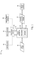
- FIG. 1 illustrates a drive system 10 that includes a power converter 12 that receives an input power 14 and produces a variable frequency power 16 to drive a driven device 18 (e.g., such as an AC electric motor).
- the power converter 12 may convert power from direct current (DC) to alternating current (AC).
- the power converter 12 converts power from an input AC signal (e.g., input power 14) and produces a different AC signal output (e.g., variable frequency power 16).
- the power converter 12 may convert the AC input signal to a desired variable frequency power 16 AC signal using a DC link.
- the power converter 12 may receive additional inputs 20 used to control or influence the conversion, such as selecting a desired waveform for the variable frequency power 16.
- the additional inputs 20 may include user inputs received from input device(s) 22 such as a human machine interface (HMI) such as a keyboard, touch screen, mouse, or other suitable interface for receiving inputs from a user for controlling power conversion.
- HMI human machine interface
- some embodiments of the power converter 12 may receive additional inputs 20 from one or more controllers 24 outside the power converter 12, such as a controller 24 used to control an industrial automation system containing the driven device 18.
- the power converter 12 may receive additional inputs 20 from one or more measurement device(s) 26.
- the measurement devices 26 may measure operation of the driven device 18 and/or conditions that may affect the driven device 18.
- the power converter 12 may include a processor 28 and memory 30.
- the processor 28 may include a central processing unit of a computing device, an application-specific instruction-set processor (ASIC), a digital signal processor, or some other suitable processor,
- the processor 28 may be used to control switches in relation to various conditions (e.g., additional inputs 20) and in the operation manners discussed below.
- the memory 30 may include a non-transitory, computer-readable medium that stores instructions for use by the processor 28.
- the memory 30 may be volatile (e.g., RAM, DRAM, SRAM) or non-volatile semi-conductor memory (e.g., ROM, EEPROM, etc.), tape, magnetic disks, optical discs (e.g., CD, DVD, etc.), or other non-transitory, computer-readable memory storage devices suitable for storing information for the power converter 12.
- volatile e.g., RAM, DRAM, SRAM
- non-volatile semi-conductor memory e.g., ROM, EEPROM, etc.
- tape e.g., magnetic disks, optical discs (e.g., CD, DVD, etc.)
- magnetic disks e.g., CD, DVD, etc.
- optical discs e.g., CD, DVD, etc.
- other non-transitory, computer-readable memory storage devices suitable for storing information for the power converter 12.
- FIG. 2 illustrates a signal generation portion 40 of the power converter 12 that is capable of producing an AC signal having a five-level or nine-level resolution.
- graph 42 of FIG. 3 illustrates a possible five-level AC signal 44 with five available power levels 46, 48, 50, 52, and 54, collectively referred to as power levels 46-54.
- the power levels 46-54 may approximately correspond to voltages between positive and negative voltages of double the voltage across each of the capacitors.
- power level 46 may be approximately equal to a negative voltage of two times the voltage across one capacitor.
- power level 48 may be approximately equal to a negative voltage of one times the voltage across one capacitor.
- Power level 50 may correspond to a neutral voltage (e.g., ground).
- the power level 52 may be approximately equal to a positive voltage of one times the voltage across one capacitor
- the power level 54 may be approximately equal to a positive voltage of two times the voltage across one capacitor.
- Power levels 46-54 to achieve five-level resolution that enables the creation of AC signal 44 that more closely emulates a sine wave than lower-resolution (e.g., two, three, or four-level signals).
- AC signals that more closely emulate a sine wave use less filtering to produce an AC signal that can be used by a driven device (e.g., driven device 18).
- the signal generation portion 40 may generate a nine-level AC signal, such as the AC signal 56 illustrated in graph 58 of FIG. 4 by using intermediate voltage levels to create voltage levels corresponding to half-step increments each corresponding to half a voltage across a capacitor.
- the power levels 60, 62, 64, 66, 68, 70, 72, 74, and 76 each corresponds to an incremental step representing a change in voltage by one-half of a voltage difference across each capacitor.
- power level 76 corresponds to approximately 2*X volts
- power level 74 corresponds to approximately 1.5X volts
- power level 72 corresponds to approximately X volts
- power level 70 corresponds to approximately X/2 volts
- power level 68 corresponds to approximately 0V.
- power level 66 corresponds to approximately negative X/2 volts
- power level 64 corresponds to approximately negative X volts
- power level 62 corresponds to approximately negative 1.5X volts
- power level 60 corresponds to negative 2*X volts.
- the signal generation portion 40 includes four DC link capacitors 80, 82, 84, and 86, collectively referred to as 80-86.
- Each of the capacitors 80-86 represents a voltage source between adjacent nodes of input voltage nodes 88, 90, 92, 94, and 96, collectively referred to as input voltage nodes 88-96.
- the capacitors 80-86 may be dedicated power supplies, such as DC power supplies, batteries, or other sources capable of generating a voltage difference between respective adjacent nodes 88-96.
- the capacitors 80-86 are connected in series such that an anode of each capacitor couples to a cathode of an adjacent capacitor. Accordingly, a voltage potential of the sum of the voltages of the capacitors 80-86 exists between a lower rail 98 and an upper rail 100.
- the signal generation portion 40 also includes a left portion 102 and the right portion 104.
- the signal generation portion 40 includes eight power switches 104, 106, 108, 110, 112, 114, 116, and 118, collectively referred to as power switches 104-118.
- one or more of the power switches 104-118 may be insulated-gate bipolar transistors (IGBT), field-effect transistors (FET), or other transistor types suitable for converting alternating connections between the capacitors 80-86 and the lower rail 98 and/or the upper rail.
- one or more of the power switches 104-118 may be a suitable thyristor, such as a gateturn off thyristor (GTO) or an integrated gate-commutated thyristor (IGCT).
- GTO gateturn off thyristor
- IGCT integrated gate-commutated thyristor
- the signal generation portion 40 also includes anti-parallel diodes 120, 122, 124, 126, 128, 130, 132, and 134, collectively referenced as diodes 120-134 each connected in anti-parallel to a respective power switch 104-118 in a switch-diode pair, such as the switch-diode pair 136.
- Each diode 120-134 acts as a clamping diode. In other words, the diodes 120-134 may reduce/eliminate a sudden voltage spike when one or more of the power switches 104-118 are toggled.
- the left portion 102 includes four switch-diode pairs (e.g., switch-diode pair 136) coupled in series between the lower rail 98 and the upper rail 96.
- the right portion 104 includes four other switch-diode pairs coupled in series between the lower rail 98 and the upper rail 96.
- the signal generation portion 40 also includes interconnection diodes 138, 140, 142, 144, 146, 148, 150, and 152, collectively referred to as diodes 138-152.
- Each interconnection diode 138-152 couples an anode and/or cathode of the capacitors 80-86 to one or more switch-diode pairs.
- the diode 138 couples the switches 104 and 106 and the diodes 120 and 122 to the anode of capacitor 86 and the cathode of capacitor 84 via node 154.
- the diode 140 couples the switches 106 and 108 and the diodes 122 and 124 to the anode of capacitor 84 and the cathode of the capacitor 82 via node 156.
- the diode the 142 couples the switches 108 and 110 and the diodes 124 and 126 to the anode of capacitor 82 and the cathode of capacitor 84 via node 158.
- the diode 144 couples the switch 110 and the diode 126 to the anode of capacitor 80 via the node 160 using the lower rail 98.
- the diode 146 couples the switch 112 and the diode 128 to the cathode of the capacitor 86 via node 162 using the upper rail 100.
- the diode 148 couples the switches 112 and 114 and the diodes 128 and 130 to the cathode of the capacitor 84 and the anode of the capacitor 86.
- the diode 150 couples the switches 114 and 116 and the diodes 130 and 132 to the cathode of the capacitor 82 and the anode of capacitor 84, and the diode 152 couples the switches 116 and 118 and the diodes 132 and 134 to the anode of the capacitor 82 and the cathode of the capacitor 80 via node 168.
- the diodes 138-152 may have different voltage ratings. For example, in some embodiments, diodes located closer in proximity to the upper rail 100 have a higher voltage rating than diodes located closer in proximity to the lower rail 98.
- diodes 144 and 152 may have voltage ratings of greater than 1000V (e.g., 1700V) while diodes 142 and 150 have voltage ratings of greater than 2000V (e.g., 3400V) and diodes 140 and 148 have voltage ratings of greater than 3000V (e.g., 5100V) and diodes 138 and 146 have voltage ratings of greater than 4000V (e.g., 6800V).
- one or more of the diodes may include diodes having lower voltage ratings coupled in series.
- a single diode type (e.g., having a voltage rating of 1700V) may be used for various voltage ratings by placing multiples of the diodes in series (e.g., two in series for 3400V, three in series for 5100V, four in series for 6800V, etc.).
- the signal generation portion 40 also includes an upper spanning reactor inductor 170 and a lower spanning reactor inductor 172.
- the upper spanning reactor inductor 170 is connected between an output node 174 and the upper rail 100.
- the lower spanning reactor inductor 172 connected between the output node 174 and the lower rail 98.
- These spanning reactor inductors 156 and 158 cause a circulating current to split voltage between the spanning reactor inductors 156 and 158 to enable the signal generation portion 40 to generate nine levels of resolution by outputting voltages at a half of a voltage across each capacitor 80-86.
- the signal generation portion 40 may operate using a nine-level operation mode or a five level operation mode.
- the switches may be operated (e.g., using the processor 28) to produce a five-level AC signal, such as AC signal 44 of FIG. 3 .
- switches 104, 106, 108, and 110 are activated while switches 112, 114, 116, and 118 are inactive.
- switches 106, 108, 110, and 112 are activated while switches 104, 114, 116, and 118 are inactive.
- switches 108, 110, 112, and 114 are activated while switches 104, 106, 116, and 118 are inactive.
- switches 110, 112, 113, and 116 are activated while switches 104, 106, 108, and 118 are deactivated.
- switches 112, 114, 116, and 118 are activated while switches 104, 106, 108, and 110 are off.
- the signal generation portion 40 may generate an AC signal such as the AC signal 44.
- the upper and lower spanning reactor inductors 170 and 172 are tied to approximately equal voltages thereby generating a voltage at the output node 174 approximately equal to the voltage exposed to each spanning reactor inductor 170 and 172.
- half step intervals may be used (e.g., the voltage levels 74, 70, 66, and 62 of FIG. 4 ).
- the spanning reactor inductors 170 and 172 may be driven to split voltages between the spanning reactor inductors 170 and 172.
- switches 104, 106, 108, 110, and 112 may be activated while switches 114, 116, 118, and 120 are off.
- the activation of switches 104, 106, 108, and 100 ties the lower spanning reactor inductor 172 to a voltage of 2X volts via the lower rail 98, where X is the voltage across each of the capacitors in volts.
- the activation of switch 112 ties the upper spanning reactor inductor 170 to a voltage of 1X volts via the upper rail 100.
- the spanning reactor inductors 170 and 172 share their voltages using a circulating current thereby causing a voltage at the output node 174 to be an average of the voltages of the inductors, such as 1.5X volts.
- the upper spanning reactor inductor 170 may be tied to a voltage of 0 volts and the lower spanning reactor inductor 172 to a voltage of 1X volts.
- the upper spanning reactor inductor 170 may be tied to 0 volts via the upper rail 100 by activating switches 112 and 114 while switches 116 and 118 are inactive, and the lower spanning reactor inductor 172 may be tied to 1X volts by activating switches 106, 108, and 110 while switch 104 remains inactive.
- the spanning reactor inductors 170 and 172 share their voltages using a circulating current thereby causing a voltage at the output node 174 to be an average of the voltages of the inductors at 0.5X volts.
- the upper spanning reactor inductor 170 may be tied to a voltage of -1X while the lower spanning reactor inductor 172 may be tied to a voltage of 0 volts.
- the upper spanning reactor inductor 170 is tied to -1X volts by activating switches 112, 114, and 116 while switch 118 remains inactive
- the lower spanning reactor inductor 170 is tied to 0 volts by activating switches 108 and 110 while switches 104 and 106 remain inactive.
- the spanning reactor inductors 170 and 172 share their voltages using a circulating current thereby causing a voltage at the output node 174 to be an average of the voltages of the inductors at - 0.5X volts.
- the upper spanning reactor inductor 170 may be tied to a voltage of -2X volts while the lower spanning reactor inductor 172 may be tied to a voltage of -1X volts.
- the upper spanning reactor inductor 170 may be tied to a voltage of -2X volts by activating switches 112, 114, 116, and 118, and the lower spanning reactor inductor 172 may be tied to a voltage of -1X volts by activating switch 110 while switches 104, 106, and 108 remain inactive.
- the spanning reactor inductors 170 and 172 share their voltages using a circulating current thereby causing a voltage at the output node 174 to be an average of the voltages of the inductors at -1.5X volts.
- portion 176 may be removed, such that the diodes 120, 122, 128, 130, 138, 140, 146 and 148, the switches 104, 106, 112, and 114, and the capacitors 86 and 86 are removed. Instead, the capacitor 82 would couple to the node 96; the diode 124 and the switch 108 would couple to the upper rail 100; and the diode 150 would couple to the upper rail 100.
- the signal generation portion 40 may be modular and be adjusted to a desired amount of power level resolution or a desired usage of power supplies (e.g., DC link capacitors).
- power supplies e.g., DC link capacitors.
- the signal generation portion 40 may balance voltages between the capacitors 80-86.
- the capacitors 80-86 may be recharged using various routing patterns for some voltage levels. For example, when the power level 62 is produced while load current is leaving the AC node 174, two possible configurations may be deployed. Either switches 110-118 may be activated to achieve the power level 62 or the switches 112-116 may be activated to achieve the same power level 62. Accordingly, by shifting which capacitors 80-86 are supplying the voltage, voltages may be balanced between the capacitors.
- voltage level 64 may be achieved by using one of the following configurations: activating switches 108, 110, and 112-116; activating switches 110 and 112-116; or activating switches 112 and 114.
- voltage level 66 may be achieved by choosing one of the following configurations: activating switches 106-110 and 112-118; activating switches 108, 110, and 112-116; activating switches 110, 112, and 114; and activating switch 112.
- voltage level 68 may be achieved by choosing one of the following configurations: activating switches 104-118; activating switches 106-116; activating switches 108-114; activating switches 110 and 112; and activating no switches.
- voltage level 70 may be achieved by choosing one of the following configurations: activating switches 104-116; activating switches 106-114; activating switches 108-112; and activating switch 110.
- activating switches 104-114 activating switches 106-112; and activating switches 108 and 110.
- voltage level 74 while current is exiting the AC node 174 one of the following configurations may be chosen: activating switches 104-112; and activating switches 106-110.
- Voltage levels 60 and 76 may be achieved using the configurations discussed above.
- each voltage level has an opposite polarity voltage level that is produced when the current is exiting/entering the AC node 174.
- voltage levels 62, 66, 70, and 74 may not be produced regardless of load current direction. Additionally, when the circulation current is discontinuous, voltage levels may be achieved using only one side of the signal generation portion.
- voltage level 60 when load current is exiting the AC node 174, voltage level 60 may be achieved by activating no switches, voltage level 64 by activating switch 110, voltage level 68 by activating switches 108 and 110, voltage level 72 by activating switches 106-110, and voltage level 76 by activating switches 104-110.
- voltage level 60 when load current is entering the AC node 174, voltage level 60 may be achieve by activating switches 112-118, voltage level 64 by activating switches 112-116, voltage level 68 by activating switches 112 and 114, voltage level 72 by activating switch 112, and voltage level 76 by activating no switches.
- the voltage level 60 may be achieved by activating switches 112-118, voltage level 64 by activating switches 110-116, voltage level 68 by activating switches 108-112, voltage level 72 by activating switches 106-112, and voltage level 76 by activating switches switches 104-110.
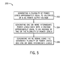
- FIG. 5 is a flow chart diagram view of a process 200 for providing a variable frequency signal from DC power supplies, such as the signal generation portion 40.
- the process 200 includes generating a plurality of power levels approximate equal to multiples of a DC power supply voltage (block 202), where the DC power supply voltage is a voltage that occurs across each power supply of the system used to generate the variable frequency signal. For example, if the power supplies of the system each generates a voltage X, in certain embodiments, the plurality of power levels may include 0, 1X, 2X, 3X, or more volts (of any polarity).
- the process 200 also includes generating one or more intermediate power levels each with a voltage approximately equal to an average of two of the plurality of power levels (block 204) using spanning reactor inductors that generate a circulating voltage within the signal generation portion 40 to average the voltages tied to each spanning reactor inductor to generate an output voltage therebetween. For example, if the plurality of power levels included a voltage level at 1X volts and a voltage level at 2X volts, the one or more intermediate power levels may include. The process 200 also includes using the plurality of power levels and the one or more intermediate power levels to generate a variable frequency signal (e.g., the AC signal 58).
- a variable frequency signal e.g., the AC signal 58
- the scalable nature of the power generation portion 40 enables a variety of power levels to increase efficiency of power generation by reducing the amount of filtration used to filter the output signal to achieve the machine voltage. A closer match between the machine voltage and output signal reduces current divergence and reduces a switching rate frequency used thereby reducing switching loss and reducing the use of snubbers.
- the spanning reactors balance the DC link voltages and filter the voltage output to increase the number of DC link voltage levels without increasing voltage stress of the switches.
- the switches 104-110 and 112-118 may generally undergo less voltage than is output.
- the switches 104-110 and 112-118 may only be used to block voltages approximately equal to a voltage across a single capacitor.
- a switch with a lower voltage rating e.g., up to 1700V.
- a power converter may be capable of conducting more current than a power converter using power switches with higher voltage ratings (e.g., 3300V or higher).
- the power converter may be manufactured more cheaply than a power converter using more expensive higher power switches (e.g., switches rated for 4500V or higher).
- the power converter may be implemented without complicated transformers or additional switches thereby reducing complexity and costs for manufacture of the power converter.
- the power converter resolution may be somewhat modular increasing the number of levels by stacking four-level modules or adding additional capacitor levels, thereby increasing flexibility of use of the power converter.
Landscapes
- Engineering & Computer Science (AREA)
- Power Engineering (AREA)
- Inverter Devices (AREA)
Abstract
Systems and methods for power conversion are disclosed. The systems and methods use generation of a plurality of power levels approximately equal to multiples of one or more power supply voltage levels along with generation of one or more intermediate power levels between levels of the plurality of power levels via spanning reactor inductors (70,72). Furthermore, the method includes generating an output signal using the generated plurality of power levels and the one or more intermediate levels.
Description
- The subject matter disclosed herein relates to power converters.
- Power converters may be used to create a variable frequency used to drive various electrical devices (e.g., AC motor) using a generated AC signal. Some driven electrical devices use high quality (e.g., high resolution) output waveforms from low, medium, or high voltages. The resolution of the AC signal may be determined by the number of levels that the power converter can produce. For example, power converters may produce AC signals with three or more available power levels (e.g., low, intermediate, high). Each additional power level adds greater resolution, but additional power levels may also increase complexity of the power converter.
- Certain embodiments commensurate in scope with the originally claimed invention are summarized below. These embodiments are not intended to limit the scope of the claimed invention, but rather these embodiments are intended only to provide a brief summary of possible forms of the invention. Indeed, the invention may encompass a variety of forms that may be similar to or different from the embodiments set forth below.
- In a first embodiment, a system for converting power includes multiple power supplies coupled in series between a first rail and a second rail. The system also includes a first spanning reactor inductor coupled between the first rail and an output node. The first spanning reactor inductor is tied to a first voltage level via the first rail. Furthermore, the system also includes a second spanning reactor inductor coupled between the second rail and the output node. The second spanning reactor inductor is tied to a second voltage level via the second rail, and the first and second spanning reactor inductors utilize a circulating current to generate a third voltage level In a second embodiment, a system for converting power includes an output node and a first spanning reactor inductor coupled between the output node and a first voltage rail. The first spanning reactor inductor has a voltage level that is tied to a voltage level of the first rail. The system also includes a second spanning reactor inductor coupled between the output node and a second voltage rail. The second spanning reactor inductor has a voltage level tied to a voltage level of the second voltage rail. The first and second spanning reactor inductors split the voltage levels of the first and second voltage rail to generate an output voltage at the output node. The system also includes one or more modular signal generation units. Each modular generation unit includes a first power supply having a first anode and a first cathode and a second power supply having a second anode and a second cathode. The second anode is coupled to the first cathode. The modular signal generation unit also includes a first channel located at a first side of the first and second power supplies. Moreover, the first channel is configured to control the voltage level of the first rail and includes a first switch-diode pair parallel to the first power supply and a second switch-diode pair parallel to the second power supply. The modular signal generation unit also includes a second channel located at an opposite side of the first and second power supplies from the first channel. The second channel is configured to control the voltage level of the second rail and includes a third switch-diode pair parallel to the first power supply and a fourth switch-diode pair parallel to the second power supply.
- In a third embodiment, method for converting power includes generating a plurality of power levels approximately equal to multiples of one or more power supply voltage levels. The method also includes generating one or more intermediate power levels between levels of the plurality of power levels via spanning reactor inductors. Furthermore, the method includes generating an output signal using the generated plurality of power levels and the one or more intermediate levels.
- These and other features, aspects, and advantages of the present invention will become better understood when the following detailed description is read with reference to the accompanying drawings in which like characters represent like parts throughout the drawings, wherein:
-
FIG. 1 is a perspective view of an embodiment of a electrical drive system having a power converter; -
FIG. 2 is a schematic diagram of an embodiment of a signal generation portion of the power converter ofFIG. 1 ; -
FIG. 3 is a graphical view of an embodiment of an output signal of the signal generation portion ofFIG. 2 having five levels of resolution; -
FIG. 4 is a graphical view of an embodiment of an output signal of the signal generation portion ofFIG. 2 having nine levels of resolution; and -
FIG. 5 is a process for converting power using the power converter ofFIG. 1 . - One or more specific embodiments of the present invention will be described below. In an effort to provide a concise description of these embodiments, all features of an actual implementation may not be described in the specification. It should be appreciated that in the development of any such actual implementation, as in any engineering or design project, numerous implementation-specific decisions must be made to achieve the developers' specific goals, such as compliance with system-related and business-related constraints, which may vary from one implementation to another. Moreover, it should be appreciated that such a development effort might be complex and time consuming, but would nevertheless be a routine undertaking of design, fabrication, and manufacture for those of ordinary skill having the benefit of this disclosure.
- When introducing elements of various embodiments of the present invention, the articles "a," "an," "the," and "said" are intended to mean that there are one or more of the elements. The terms "comprising," "including," and "having" are intended to be inclusive and mean that there may be additional elements other than the listed elements.
- As will be discussed below, this disclosure relates to a power converter that includes a simple method of achieving high voltage, low distortion power converters. The power converters are capable of variable frequencies using a small footprint is available while providing a cheaper and smaller power generation system than is possible using magnetic components. Furthermore, the scalable nature of power generators of the power converters enable a variety of power levels to increase efficiency of power generation by reducing the amount of filtration used to filter the output signal to achieve a machine voltage. A closer match between the machine voltage and output signal reduces current divergence and reduces a switching rate frequency used thereby reducing switching loss and reducing the use of snubbers.
- Also, due to the amount of power used in some power converters, power switches used in some power converters are used with higher voltage ratings (e.g., 3300V). However, in the signal generation portion discussed below, the spanning reactor inductors used in the power converters balance the DC link voltages and filter the voltage output to increase the number of DC link voltage levels without increasing voltage stress of the switches. By using switches with lower voltage ratings (e.g., up to 1700V), a power converter may be capable of conducting more current than a power converter using power switches with higher voltage ratings (e.g., 3300V or higher). Furthermore, the power converter may be manufactured more cheaply than a power converter using more expensive higher power switches (e.g., switches rated for 4500V or higher). Moreover, the power converter may be implemented without complicated transformers or additional switches thereby reducing complexity and costs for manufacture of the power converter. Furthermore, the power converter resolution may be modular through increasing the number of levels by stacking four-level modules or adding additional capacitor levels, thereby increasing flexibility of use of the power converter.
-
FIG. 1 illustrates adrive system 10 that includes apower converter 12 that receives aninput power 14 and produces avariable frequency power 16 to drive a driven device 18 (e.g., such as an AC electric motor). In some embodiments, thepower converter 12 may convert power from direct current (DC) to alternating current (AC). In other embodiments, thepower converter 12 converts power from an input AC signal (e.g., input power 14) and produces a different AC signal output (e.g., variable frequency power 16). For example, thepower converter 12 may convert the AC input signal to a desiredvariable frequency power 16 AC signal using a DC link. - In some embodiments, the
power converter 12 may receiveadditional inputs 20 used to control or influence the conversion, such as selecting a desired waveform for thevariable frequency power 16. In some embodiments, theadditional inputs 20 may include user inputs received from input device(s) 22 such as a human machine interface (HMI) such as a keyboard, touch screen, mouse, or other suitable interface for receiving inputs from a user for controlling power conversion. Additionally or alternatively, some embodiments of thepower converter 12 may receiveadditional inputs 20 from one ormore controllers 24 outside thepower converter 12, such as acontroller 24 used to control an industrial automation system containing the drivendevice 18. Furthermore, in some embodiments, thepower converter 12 may receiveadditional inputs 20 from one or more measurement device(s) 26. For example, in certain embodiments, themeasurement devices 26 may measure operation of the drivendevice 18 and/or conditions that may affect the drivendevice 18. - In certain embodiments, the
power converter 12 may include aprocessor 28 andmemory 30. In such embodiments, theprocessor 28 may include a central processing unit of a computing device, an application-specific instruction-set processor (ASIC), a digital signal processor, or some other suitable processor, In certain embodiments, theprocessor 28 may be used to control switches in relation to various conditions (e.g., additional inputs 20) and in the operation manners discussed below. Thememory 30 may include a non-transitory, computer-readable medium that stores instructions for use by theprocessor 28. In some embodiments, thememory 30 may be volatile (e.g., RAM, DRAM, SRAM) or non-volatile semi-conductor memory (e.g., ROM, EEPROM, etc.), tape, magnetic disks, optical discs (e.g., CD, DVD, etc.), or other non-transitory, computer-readable memory storage devices suitable for storing information for thepower converter 12. -
FIG. 2 illustrates asignal generation portion 40 of thepower converter 12 that is capable of producing an AC signal having a five-level or nine-level resolution. For example,graph 42 ofFIG. 3 illustrates a possible five-level AC signal 44 with fiveavailable power levels power level 46 may be approximately equal to a negative voltage of two times the voltage across one capacitor. Similarly,power level 48 may be approximately equal to a negative voltage of one times the voltage across onecapacitor. Power level 50 may correspond to a neutral voltage (e.g., ground). Likewise, thepower level 52 may be approximately equal to a positive voltage of one times the voltage across one capacitor, and the power level 54 may be approximately equal to a positive voltage of two times the voltage across one capacitor. Power levels 46-54 to achieve five-level resolution that enables the creation ofAC signal 44 that more closely emulates a sine wave than lower-resolution (e.g., two, three, or four-level signals). AC signals that more closely emulate a sine wave use less filtering to produce an AC signal that can be used by a driven device (e.g., driven device 18). - In addition to the five-
level AC signal 44, thesignal generation portion 40 may generate a nine-level AC signal, such as theAC signal 56 illustrated ingraph 58 ofFIG. 4 by using intermediate voltage levels to create voltage levels corresponding to half-step increments each corresponding to half a voltage across a capacitor. In some embodiments, thepower levels power level 76 corresponds to approximately 2*X volts, power level 74 corresponds to approximately 1.5X volts,power level 72 corresponds to approximately X volts,power level 70 corresponds to approximately X/2 volts, andpower level 68 corresponds to approximately 0V. Similarly,power level 66 corresponds to approximately negative X/2 volts,power level 64 corresponds to approximately negative X volts,power level 62 corresponds to approximately negative 1.5X volts, andpower level 60 corresponds to negative 2*X volts. - Returning to
FIG. 2 , thesignal generation portion 40 includes fourDC link capacitors input voltage nodes lower rail 98 and anupper rail 100. Thesignal generation portion 40 also includes aleft portion 102 and theright portion 104. - The
signal generation portion 40 includes eightpower switches lower rail 98 and/or the upper rail. In certain embodiments, one or more of the power switches 104-118 may be a suitable thyristor, such as a gateturn off thyristor (GTO) or an integrated gate-commutated thyristor (IGCT). Thesignal generation portion 40 also includesanti-parallel diodes diode pair 136. Each diode 120-134 acts as a clamping diode. In other words, the diodes 120-134 may reduce/eliminate a sudden voltage spike when one or more of the power switches 104-118 are toggled. Theleft portion 102 includes four switch-diode pairs (e.g., switch-diode pair 136) coupled in series between thelower rail 98 and theupper rail 96. Similarly, theright portion 104 includes four other switch-diode pairs coupled in series between thelower rail 98 and theupper rail 96. - The
signal generation portion 40 also includesinterconnection diodes diode 138 couples theswitches diodes capacitor 86 and the cathode ofcapacitor 84 vianode 154. Similarly, thediode 140 couples theswitches diodes capacitor 84 and the cathode of thecapacitor 82 vianode 156. Likewise, the diode the 142 couples theswitches diodes capacitor 82 and the cathode ofcapacitor 84 vianode 158. Moreover, thediode 144 couples theswitch 110 and thediode 126 to the anode ofcapacitor 80 via thenode 160 using thelower rail 98. In theright portion 104, thediode 146 couples theswitch 112 and thediode 128 to the cathode of thecapacitor 86 vianode 162 using theupper rail 100. Similarly, thediode 148 couples theswitches diodes capacitor 84 and the anode of thecapacitor 86. Thediode 150 couples theswitches diodes capacitor 82 and the anode ofcapacitor 84, and thediode 152 couples theswitches diodes capacitor 82 and the cathode of thecapacitor 80 vianode 168. - In some embodiments, as discussed below, the diodes 138-152 may have different voltage ratings. For example, in some embodiments, diodes located closer in proximity to the
upper rail 100 have a higher voltage rating than diodes located closer in proximity to thelower rail 98. For example, in certain embodiments with the capacitors 80-86 having a voltage capacity of 1000V,diodes diodes diodes diodes - The
signal generation portion 40 also includes an upper spanningreactor inductor 170 and a lower spanningreactor inductor 172. The upper spanningreactor inductor 170 is connected between anoutput node 174 and theupper rail 100. Similarly, the lower spanningreactor inductor 172 connected between theoutput node 174 and thelower rail 98. These spanningreactor inductors reactor inductors signal generation portion 40 to generate nine levels of resolution by outputting voltages at a half of a voltage across each capacitor 80-86. - Using the switches 104-118 and/or the spanning
reactor inductors signal generation portion 40 may operate using a nine-level operation mode or a five level operation mode. During five-level operation the switches may be operated (e.g., using the processor 28) to produce a five-level AC signal, such asAC signal 44 ofFIG. 3 . For example, to generate the voltage level 54, switches 104, 106, 108, and 110 are activated whileswitches voltage level 52, switches 106, 108, 110, and 112 are activated whileswitches voltage level 50, switches 108, 110, 112, and 114 are activated whileswitches voltage level 48switches switches voltage level 46, switches 112, 114, 116, and 118 are activated whileswitches signal generation portion 40 may generate an AC signal such as theAC signal 44. In such embodiments, the upper and lower spanningreactor inductors output node 174 approximately equal to the voltage exposed to each spanningreactor inductor - If additional resolution is desired, half step intervals may be used (e.g., the
voltage levels FIG. 4 ). To achieve such intervals, the spanningreactor inductors reactor inductors switches switches reactor inductor 172 to a voltage of 2X volts via thelower rail 98, where X is the voltage across each of the capacitors in volts. The activation ofswitch 112 ties the upper spanningreactor inductor 170 to a voltage of 1X volts via theupper rail 100. The spanningreactor inductors output node 174 to be an average of the voltages of the inductors, such as 1.5X volts. Similarly, to achieve thevoltage level 50 of 0.5X volts, the upper spanningreactor inductor 170 may be tied to a voltage of 0 volts and the lower spanningreactor inductor 172 to a voltage of 1X volts. In certain embodiments, the upper spanningreactor inductor 170 may be tied to 0 volts via theupper rail 100 by activatingswitches switches reactor inductor 172 may be tied to 1X volts by activatingswitches switch 104 remains inactive. The spanningreactor inductors output node 174 to be an average of the voltages of the inductors at 0.5X volts. To achieve avoltage level 66 of -0.5X volts, the upper spanningreactor inductor 170 may be tied to a voltage of -1X while the lower spanningreactor inductor 172 may be tied to a voltage of 0 volts. In some embodiments, the upper spanningreactor inductor 170 is tied to -1X volts by activatingswitches switch 118 remains inactive, and the lower spanningreactor inductor 170 is tied to 0 volts by activatingswitches switches reactor inductors output node 174 to be an average of the voltages of the inductors at - 0.5X volts. To achieve thevoltage level 62 of -1.5X volts, the upper spanningreactor inductor 170 may be tied to a voltage of -2X volts while the lower spanningreactor inductor 172 may be tied to a voltage of -1X volts. In some embodiments, the upper spanningreactor inductor 170 may be tied to a voltage of -2X volts by activatingswitches reactor inductor 172 may be tied to a voltage of -1X volts by activatingswitch 110 whileswitches reactor inductors output node 174 to be an average of the voltages of the inductors at -1.5X volts. - Although the foregoing discussion specifically discusses the creation of a nine-
level AC signal 58 using four sources, some embodiments may use different numbers of power supplies and available levels by adding/subtracting two switch-diode pairs and diodes along with capacitors. For example, to modify thesignal generation portion 40 to generate a five level signal using two capacitors,portion 176 may be removed, such that thediodes switches capacitors capacitor 82 would couple to thenode 96; thediode 124 and theswitch 108 would couple to theupper rail 100; and thediode 150 would couple to theupper rail 100. To modify the signal generation portion to generate a thirteen level signal using six capacitors, another section may be added to thesignal generation portion 40 that is similar to theportion 176 and inserted between theportion 176 and theupper rail 100. Thus, thesignal generation portion 40 may be modular and be adjusted to a desired amount of power level resolution or a desired usage of power supplies (e.g., DC link capacitors). In other words, using the above-described system allows for the production of a variable frequency signal with a number of available power levels that is one more than twice the number of power supplies (e.g., batteries, capacitors, etc.) used. Accordingly, the number of available levels of resolution may be found using the following equation:
, where nL is the number of available levels and nS is the number of sources used to generating the variable frequency signal. - Returning to
FIG. 2 , in some embodiments, thesignal generation portion 40 may balance voltages between the capacitors 80-86. In certain embodiments, the capacitors 80-86 may be recharged using various routing patterns for some voltage levels. For example, when thepower level 62 is produced while load current is leaving theAC node 174, two possible configurations may be deployed. Either switches 110-118 may be activated to achieve thepower level 62 or the switches 112-116 may be activated to achieve thesame power level 62. Accordingly, by shifting which capacitors 80-86 are supplying the voltage, voltages may be balanced between the capacitors. Similarly, while current is exiting theAC node 174,voltage level 64 may be achieved by using one of the following configurations: activatingswitches switches 110 and 112-116; or activatingswitches AC node 174,voltage level 66 may be achieved by choosing one of the following configurations: activating switches 106-110 and 112-118; activatingswitches switches switch 112. Likewise, while current is exiting theAC node 174,voltage level 68 may be achieved by choosing one of the following configurations: activating switches 104-118; activating switches 106-116; activating switches 108-114; activatingswitches AC node 174,voltage level 70 may be achieved by choosing one of the following configurations: activating switches 104-116; activating switches 106-114; activating switches 108-112; and activatingswitch 110. To achievevoltage level 72 while current is exiting theAC node 174 one of the following configurations may be chosen: activating switches 104-114; activating switches 106-112; and activatingswitches AC node 174 one of the following configurations may be chosen: activating switches 104-112; and activating switches 106-110.Voltage levels - When load current is entering the
AC node 174 the configurations produce opposite polarity voltage levels. For example, if current is entering theAC node 174, the configurations discussed above regardingvoltage level 62 would instead produce voltage level 74. In other words, each voltage level has an opposite polarity voltage level that is produced when the current is exiting/entering theAC node 174. Furthermore, in some embodiments, when a circulating current is discontinuous thevoltage levels AC node 174,voltage level 60 may be achieved by activating no switches,voltage level 64 by activatingswitch 110,voltage level 68 by activatingswitches voltage level 72 by activating switches 106-110, andvoltage level 76 by activating switches 104-110. Likewise, when load current is entering theAC node 174,voltage level 60 may be achieve by activating switches 112-118,voltage level 64 by activating switches 112-116,voltage level 68 by activatingswitches voltage level 72 by activatingswitch 112, andvoltage level 76 by activating no switches. If the load current is indeterminate and the circulating current is discontinuous, thevoltage level 60 may be achieved by activating switches 112-118,voltage level 64 by activating switches 110-116,voltage level 68 by activating switches 108-112,voltage level 72 by activating switches 106-112, andvoltage level 76 by activating switches switches 104-110. -
FIG. 5 is a flow chart diagram view of aprocess 200 for providing a variable frequency signal from DC power supplies, such as thesignal generation portion 40. Theprocess 200 includes generating a plurality of power levels approximate equal to multiples of a DC power supply voltage (block 202), where the DC power supply voltage is a voltage that occurs across each power supply of the system used to generate the variable frequency signal. For example, if the power supplies of the system each generates a voltage X, in certain embodiments, the plurality of power levels may include 0, 1X, 2X, 3X, or more volts (of any polarity). Theprocess 200 also includes generating one or more intermediate power levels each with a voltage approximately equal to an average of two of the plurality of power levels (block 204) using spanning reactor inductors that generate a circulating voltage within thesignal generation portion 40 to average the voltages tied to each spanning reactor inductor to generate an output voltage therebetween. For example, if the plurality of power levels included a voltage level at 1X volts and a voltage level at 2X volts, the one or more intermediate power levels may include. Theprocess 200 also includes using the plurality of power levels and the one or more intermediate power levels to generate a variable frequency signal (e.g., the AC signal 58). - By using the above-described switching topology and method, a simple method of achieving high voltage, low distortion power converters capable of variable frequencies using a small footprint is available while providing a cheaper and smaller power generation system than is possible using magnetic components. Furthermore, the scalable nature of the
power generation portion 40 enables a variety of power levels to increase efficiency of power generation by reducing the amount of filtration used to filter the output signal to achieve the machine voltage. A closer match between the machine voltage and output signal reduces current divergence and reduces a switching rate frequency used thereby reducing switching loss and reducing the use of snubbers. - Also, due to the amount of power used in some power converters, power switches are used with higher voltage ratings (e.g., 3300V). However, in the
signal generation portion 40 discussed above, the spanning reactors balance the DC link voltages and filter the voltage output to increase the number of DC link voltage levels without increasing voltage stress of the switches. For example, the switches 104-110 and 112-118 (and their respective anti-parallel diodes) may generally undergo less voltage than is output. For example, in some embodiments, the switches 104-110 and 112-118 (and their respective anti-parallel diodes) may only be used to block voltages approximately equal to a voltage across a single capacitor. By reducing the amount of voltage that a switch blocks, a switch with a lower voltage rating (e.g., up to 1700V). By using switches with lower voltage ratings (e.g., up to 1700V), a power converter may be capable of conducting more current than a power converter using power switches with higher voltage ratings (e.g., 3300V or higher). Furthermore, the power converter may be manufactured more cheaply than a power converter using more expensive higher power switches (e.g., switches rated for 4500V or higher). Moreover, the power converter may be implemented without complicated transformers or additional switches thereby reducing complexity and costs for manufacture of the power converter. Furthermore, the power converter resolution may be somewhat modular increasing the number of levels by stacking four-level modules or adding additional capacitor levels, thereby increasing flexibility of use of the power converter. - This written description uses examples to disclose the invention, including the best mode, and also to enable any person skilled in the art to practice the invention, including making and using any devices or systems and performing any incorporated methods. The patentable scope of the invention is defined by the claims, and may include other examples that occur to those skilled in the art. Such other examples are intended to be within the scope of the claims if they have structural elements that do not differ from the literal language of the claims, or if they include equivalent structural elements with insubstantial differences from the literal language of the claims.
Claims (13)
- A system for converting power comprising:a plurality of power supplies (80-86) coupled in series between a first rail (100) and a second rail (90);a first spanning reactor inductor (170) coupled between the first rail (100) and an output node (174), wherein the first spanning reactor inductor (170) is tied to a first voltage level via the first rail (100); anda second spanning reactor inductor (172) coupled between the second rail (90) and the output node (174), wherein the second spanning reactor inductor (172) is tied to a second voltage level via the second rail (90), wherein the first and second spanning reactor inductors (170,172) utilize a circulating current to generate a third voltage level.
- The system of claim 1, comprising:a first portion comprising:a first plurality of switch-diode pairs (112-118,128-134) configured to couple the first rail (100) to the first voltage level (54); anda first plurality of interconnecting diodes (146-152) each coupling one or more of the first plurality of switch-diode pairs (112-118,128-134) to a respective power supply of the plurality of power supplies (80-86); anda second portion (102) comprising:a second plurality of switch-diode pairs (104-110,120-152) configured to couple the second rail (90) to the second voltage level (52); anda first plurality of interconnecting diodes (138-152) each coupling one or more of the first plurality of switch-diode pairs (104-110,120-126) to a respective power supply of the plurality of power supplies (80-86), wherein the first portion (102) and the second portion are substantially symmetrical about the plurality of power supplies (80-86).
- The system of claim 1 or 2, wherein the first voltage level comprises a first multiple of a supply voltage provided by each of the plurality of power supplies 80-86), and the second voltage level comprises a second multiple of the supply voltage.
- The system of claim 3, wherein the first voltage level is different than the second voltage level, wherein the third voltage level is between multiples of the supply voltage.
- The system of claim 4, wherein the third voltage level comprises a non-integer multiple of the supply voltage.
- The system of any preceding claim, wherein the third voltage level is an average of the first voltage and the second voltage.
- The system of any of claims 2 to 6, wherein the first and second plurality of switch-diode pairs (112-118,128-134) comprise insulated-gate bipolar transistors (IGBTs), integrated gate-commutated thyristors (IGCTs), gate-turn off thyristors (GTOs) as a switch of each switch diode pair, or a combination thereof.
- The system of any preceding claim, wherein the plurality of power supplies (80-86) each comprises capacitors, chemical batteries, or a combination thereof.
- The system of claim 8, when dependent on claim 2, wherein each of the plurality of power supplies (80-86) each comprises DC link capacitors, wherein the first and second portions are configured to provide one or more configurations for each desired output voltage, wherein the one or more configurations for each desired output voltage allows capacitor balancing between the DC link capacitors (80-86) by varying which of the DC link capacitors are discharging or charging.
- The system of any preceding claim, wherein the first and second spanning reactor inductors (170,172) are configured to generate an output signal with a number of available levels of resolution.
- A method (200) for converting power comprising:generating (202) a plurality of power levels (46-54,60-76) approximately equal to multiples of one or more power supply voltage levels;generating (204) one or more intermediate power levels between levels of the plurality of power levels (46-54,60-76) via spanning reactor inductors (70,72); andgenerating an output signal (58) using the generated plurality of power levels (46-54,60-76) and the one or more intermediate levels.
- The method of claim 11, wherein generating the one or more intermediate power levels comprises inducing a circulating current using the spanning reactor inductors (70,72) to average two or more power levels of the plurality of power levels.
- The method of claim 11 or 12, comprising driving an AC motor using the output signal.
Applications Claiming Priority (1)
| Application Number | Priority Date | Filing Date | Title |
|---|---|---|---|
| US14/163,649 US20150214830A1 (en) | 2014-01-24 | 2014-01-24 | System and method of power conversion |
Publications (1)
| Publication Number | Publication Date |
|---|---|
| EP2899869A1 true EP2899869A1 (en) | 2015-07-29 |
Family
ID=52391847
Family Applications (1)
| Application Number | Title | Priority Date | Filing Date |
|---|---|---|---|
| EP15152206.7A Withdrawn EP2899869A1 (en) | 2014-01-24 | 2015-01-22 | System and method of power conversion |
Country Status (3)
| Country | Link |
|---|---|
| US (1) | US20150214830A1 (en) |
| EP (1) | EP2899869A1 (en) |
| CN (1) | CN104811066A (en) |
Cited By (2)
| Publication number | Priority date | Publication date | Assignee | Title |
|---|---|---|---|---|
| GB2571721A (en) * | 2018-03-05 | 2019-09-11 | Ge Aviat Systems Ltd | AC power source |
| US11142332B2 (en) | 2018-07-13 | 2021-10-12 | Ge Aviation Systems Limited | Power supply and method having series-arranged units |
Families Citing this family (2)
| Publication number | Priority date | Publication date | Assignee | Title |
|---|---|---|---|---|
| US10615727B2 (en) * | 2018-08-27 | 2020-04-07 | General Electric Company | Dynamic brake circuit assembly for a wind turbine |
| CN113824335B (en) * | 2021-09-18 | 2023-11-07 | 厦门大学 | Single-phase Z-source boost type variable-frequency alternating current-alternating current converter |
Citations (3)
| Publication number | Priority date | Publication date | Assignee | Title |
|---|---|---|---|---|
| US20060044857A1 (en) * | 2004-08-25 | 2006-03-02 | Lemak Thomas A | Transformerless multi-level power converter |
| WO2011124260A1 (en) * | 2010-04-08 | 2011-10-13 | Areva T&D Uk Limited | Modularised converter for hvdc and statcom |
| JP2012044839A (en) * | 2010-08-23 | 2012-03-01 | Tokyo Institute Of Technology | Power converter |
Family Cites Families (6)
| Publication number | Priority date | Publication date | Assignee | Title |
|---|---|---|---|---|
| EP0838855B1 (en) * | 1991-09-20 | 2004-11-24 | Hitachi, Ltd. | Semiconductor module |
| US7285876B1 (en) * | 2006-05-01 | 2007-10-23 | Raytheon Company | Regenerative gate drive circuit for power MOSFET |
| JP2007325480A (en) * | 2006-06-05 | 2007-12-13 | National Institute Of Advanced Industrial & Technology | Power integrated circuit |
| US7986535B2 (en) * | 2007-07-17 | 2011-07-26 | Raytheon Company | Methods and apparatus for a cascade converter using series resonant cells with zero voltage switching |
| US8582331B2 (en) * | 2009-07-20 | 2013-11-12 | Vincotech Holdings S.à.r.l. | Inverter topologies usable with reactive power |
| WO2012040257A1 (en) * | 2010-09-21 | 2012-03-29 | Curtiss-Wright Electro-Mechanical Corporation | Two terminal multilevel converter |
-
2014
- 2014-01-24 US US14/163,649 patent/US20150214830A1/en not_active Abandoned
-
2015
- 2015-01-22 EP EP15152206.7A patent/EP2899869A1/en not_active Withdrawn
- 2015-01-23 CN CN201510034471.9A patent/CN104811066A/en active Pending
Patent Citations (3)
| Publication number | Priority date | Publication date | Assignee | Title |
|---|---|---|---|---|
| US20060044857A1 (en) * | 2004-08-25 | 2006-03-02 | Lemak Thomas A | Transformerless multi-level power converter |
| WO2011124260A1 (en) * | 2010-04-08 | 2011-10-13 | Areva T&D Uk Limited | Modularised converter for hvdc and statcom |
| JP2012044839A (en) * | 2010-08-23 | 2012-03-01 | Tokyo Institute Of Technology | Power converter |
Cited By (4)
| Publication number | Priority date | Publication date | Assignee | Title |
|---|---|---|---|---|
| GB2571721A (en) * | 2018-03-05 | 2019-09-11 | Ge Aviat Systems Ltd | AC power source |
| GB2571721B (en) * | 2018-03-05 | 2021-01-20 | Ge Aviat Systems Ltd | AC power source |
| US10958075B2 (en) | 2018-03-05 | 2021-03-23 | Ge Aviation Systems Limited | AC power source |
| US11142332B2 (en) | 2018-07-13 | 2021-10-12 | Ge Aviation Systems Limited | Power supply and method having series-arranged units |
Also Published As
| Publication number | Publication date |
|---|---|
| CN104811066A (en) | 2015-07-29 |
| US20150214830A1 (en) | 2015-07-30 |
Similar Documents
| Publication | Publication Date | Title |
|---|---|---|
| JP6123219B2 (en) | Multi-level power converter | |
| US9231492B2 (en) | System and method of power conversion | |
| US20170163171A1 (en) | Apparatus and method for controlling asymmetric modular multilevel converter | |
| JP6232944B2 (en) | Multi-level power converter | |
| US11011997B2 (en) | Pulse width modulation control for a multilevel converter | |
| KR101980691B1 (en) | Synthetic test circuit for valve test of hvdc | |
| WO2011120970A1 (en) | Multilevel inverter | |
| US20170194877A1 (en) | Hybrid multilevel inverter | |
| EP2899869A1 (en) | System and method of power conversion | |
| Karasani et al. | A modified switched-diode topology for cascaded multilevel inverters | |
| Schmitt et al. | A high current, high frequency modular multiphase multilevel converter for power hardware-in-the-loop emulation | |
| Devi et al. | Comparative study on different five level inverter topologies | |
| JP4643117B2 (en) | Multi-cell energy converter | |
| Yarlagadda et al. | A modified seven level cascaded H bridge inverter | |
| Sarbanzadeh et al. | A new sub-multilevel inverter with reduced number of components | |
| Kucka et al. | Control for quasi two-level PWM operation of modular multilevel converter | |
| Ibrahim et al. | Comparative analysis of PWM techniques for three level diode clamped voltage source inverter | |
| JP5724486B2 (en) | Multi-level power converter | |
| Thakre et al. | Symmetrical and asymmetrical multilevel inverter using less number of switches | |
| Kadri et al. | Comparison between the most popular structures of multilevel inverters and the packed U cell structure | |
| Renani et al. | Performance evaluation of multicarrier PWM methods for cascaded H-bridge multilevel inverter | |
| US20140300195A1 (en) | Power converter capable of outputting a plurality of different levels of voltages | |
| JP6428859B1 (en) | Multi-level power converter | |
| Das et al. | Multilevel converter topology suitable for separate and variable magnitude of DC sources | |
| Thakre et al. | Design and implementation of symmetric and asymmetric structure for multilevel inverter |
Legal Events
| Date | Code | Title | Description |
|---|---|---|---|
| PUAI | Public reference made under article 153(3) epc to a published international application that has entered the european phase |
Free format text: ORIGINAL CODE: 0009012 |
|
| 17P | Request for examination filed |
Effective date: 20150122 |
|
| AK | Designated contracting states |
Kind code of ref document: A1 Designated state(s): AL AT BE BG CH CY CZ DE DK EE ES FI FR GB GR HR HU IE IS IT LI LT LU LV MC MK MT NL NO PL PT RO RS SE SI SK SM TR |
|
| AX | Request for extension of the european patent |
Extension state: BA ME |
|
| STAA | Information on the status of an ep patent application or granted ep patent |
Free format text: STATUS: THE APPLICATION IS DEEMED TO BE WITHDRAWN |
|
| 18D | Application deemed to be withdrawn |
Effective date: 20160130 |