EP2899760A1 - Semiconductor device for optical applications and method of producing such a semiconductor device - Google Patents
Semiconductor device for optical applications and method of producing such a semiconductor device Download PDFInfo
- Publication number
- EP2899760A1 EP2899760A1 EP14152688.9A EP14152688A EP2899760A1 EP 2899760 A1 EP2899760 A1 EP 2899760A1 EP 14152688 A EP14152688 A EP 14152688A EP 2899760 A1 EP2899760 A1 EP 2899760A1
- Authority
- EP
- European Patent Office
- Prior art keywords
- layer
- filter
- sensor
- semiconductor body
- substrate
- Prior art date
- Legal status (The legal status is an assumption and is not a legal conclusion. Google has not performed a legal analysis and makes no representation as to the accuracy of the status listed.)
- Granted
Links
Images




Classifications
-
- H—ELECTRICITY
- H10—SEMICONDUCTOR DEVICES; ELECTRIC SOLID-STATE DEVICES NOT OTHERWISE PROVIDED FOR
- H10F—INORGANIC SEMICONDUCTOR DEVICES SENSITIVE TO INFRARED RADIATION, LIGHT, ELECTROMAGNETIC RADIATION OF SHORTER WAVELENGTH OR CORPUSCULAR RADIATION
- H10F39/00—Integrated devices, or assemblies of multiple devices, comprising at least one element covered by group H10F30/00, e.g. radiation detectors comprising photodiode arrays
- H10F39/80—Constructional details of image sensors
- H10F39/806—Optical elements or arrangements associated with the image sensors
-
- H—ELECTRICITY
- H10—SEMICONDUCTOR DEVICES; ELECTRIC SOLID-STATE DEVICES NOT OTHERWISE PROVIDED FOR
- H10F—INORGANIC SEMICONDUCTOR DEVICES SENSITIVE TO INFRARED RADIATION, LIGHT, ELECTROMAGNETIC RADIATION OF SHORTER WAVELENGTH OR CORPUSCULAR RADIATION
- H10F39/00—Integrated devices, or assemblies of multiple devices, comprising at least one element covered by group H10F30/00, e.g. radiation detectors comprising photodiode arrays
- H10F39/011—Manufacture or treatment of image sensors covered by group H10F39/12
- H10F39/026—Wafer-level processing
-
- H—ELECTRICITY
- H10—SEMICONDUCTOR DEVICES; ELECTRIC SOLID-STATE DEVICES NOT OTHERWISE PROVIDED FOR
- H10F—INORGANIC SEMICONDUCTOR DEVICES SENSITIVE TO INFRARED RADIATION, LIGHT, ELECTROMAGNETIC RADIATION OF SHORTER WAVELENGTH OR CORPUSCULAR RADIATION
- H10F39/00—Integrated devices, or assemblies of multiple devices, comprising at least one element covered by group H10F30/00, e.g. radiation detectors comprising photodiode arrays
- H10F39/80—Constructional details of image sensors
- H10F39/811—Interconnections
-
- H—ELECTRICITY
- H10—SEMICONDUCTOR DEVICES; ELECTRIC SOLID-STATE DEVICES NOT OTHERWISE PROVIDED FOR
- H10W—GENERIC PACKAGES, INTERCONNECTIONS, CONNECTORS OR OTHER CONSTRUCTIONAL DETAILS OF DEVICES COVERED BY CLASS H10
- H10W20/00—Interconnections in chips, wafers or substrates
- H10W20/01—Manufacture or treatment
- H10W20/021—Manufacture or treatment of interconnections within wafers or substrates
- H10W20/023—Manufacture or treatment of interconnections within wafers or substrates the interconnections being through-semiconductor vias
- H10W20/0234—Manufacture or treatment of interconnections within wafers or substrates the interconnections being through-semiconductor vias comprising etching via holes that stop on pads or on electrodes
-
- H—ELECTRICITY
- H10—SEMICONDUCTOR DEVICES; ELECTRIC SOLID-STATE DEVICES NOT OTHERWISE PROVIDED FOR
- H10W—GENERIC PACKAGES, INTERCONNECTIONS, CONNECTORS OR OTHER CONSTRUCTIONAL DETAILS OF DEVICES COVERED BY CLASS H10
- H10W20/00—Interconnections in chips, wafers or substrates
- H10W20/01—Manufacture or treatment
- H10W20/021—Manufacture or treatment of interconnections within wafers or substrates
- H10W20/023—Manufacture or treatment of interconnections within wafers or substrates the interconnections being through-semiconductor vias
- H10W20/0242—Manufacture or treatment of interconnections within wafers or substrates the interconnections being through-semiconductor vias comprising etching via holes from the back sides of the chips, wafers or substrates
-
- H—ELECTRICITY
- H10—SEMICONDUCTOR DEVICES; ELECTRIC SOLID-STATE DEVICES NOT OTHERWISE PROVIDED FOR
- H10W—GENERIC PACKAGES, INTERCONNECTIONS, CONNECTORS OR OTHER CONSTRUCTIONAL DETAILS OF DEVICES COVERED BY CLASS H10
- H10W20/00—Interconnections in chips, wafers or substrates
- H10W20/20—Interconnections within wafers or substrates, e.g. through-silicon vias [TSV]
-
- H—ELECTRICITY
- H10—SEMICONDUCTOR DEVICES; ELECTRIC SOLID-STATE DEVICES NOT OTHERWISE PROVIDED FOR
- H10W—GENERIC PACKAGES, INTERCONNECTIONS, CONNECTORS OR OTHER CONSTRUCTIONAL DETAILS OF DEVICES COVERED BY CLASS H10
- H10W20/00—Interconnections in chips, wafers or substrates
- H10W20/20—Interconnections within wafers or substrates, e.g. through-silicon vias [TSV]
- H10W20/211—Through-semiconductor vias, e.g. TSVs
- H10W20/216—Through-semiconductor vias, e.g. TSVs characterised by dielectric material at least partially filling the via holes, e.g. covering the through-semiconductor vias in the via holes
Definitions
- US 2007/249095 A1 discloses a semiconductor package including an infrared filter bonded to a wafer.
- a suitable infrared filter layer is applied on a glass sheet having the same dimensions as the wafer.
- the glass sheet is bonded to the wafer with the filter layer facing towards the wafer, which is subsequently thinned.
- the resulting total thickness of the wafer and the filter is not greater than the initial thickness of the wafer.
- Via holes are formed through the wafer from the side opposite the filter to contact pad electrodes that are located between the wafer and the filter.
- DE 102009004725 A1 describes stacked semiconductor devices with a bond layer including a buried contact pad, which is connected with a metal layer on the upper surface of one of the wafers by means of a metallization in a through-wafer via.
- the contact pad and the surface metal layer can be connected with a metal plane of a wiring or with a contact pad that is provided for a connection with a further semiconductor device.
- the semiconductor device comprises a semiconductor substrate with a main surface, a sensor arranged in the substrate at the main surface, a filter arranged above the sensor, and a through-substrate via penetrating the substrate outside the sensor.
- a frame layer is arranged above the main surface above the through-substrate via. The frame layer does not cover the filter, which is on a level with the frame layer.
- the frame layer may be a silicon layer.
- the sensor may be an optical sensor
- the filter may be an optical filter, especially an interference filter, which may especially be used as an ultraviolet and/or infrared cut-off filter, a photopic filter, a colour filter, a band pass filter or any combination thereof.
- inventions comprise a dielectric layer on the main surface, the filter and the frame layer being arranged on the dielectric layer.
- Further embodiments comprise a metal layer arranged in the dielectric layer, a contact area of the metal layer between the through-substrate via and the frame layer, and a metal layer of the through-substrate via contacting the contact area.
- Further embodiments comprise a passivation layer arranged in the dielectric layer.
- the passivation layer comprises a material different from the dielectric layer and an opening between the sensor and the filter.
- the method of producing a semiconductor device comprises arranging a sensor at a main surface of a semiconductor substrate, arranging a filter above the sensor, and forming a through-substrate via penetrating the substrate outside the sensor.
- a semiconductor body is applied above the main surface and then partially removed at least in an area above the sensor. A portion of the semiconductor body remains above the through-substrate via.
- the semiconductor body is provided with a recess and applied with the recess facing the sensor.
- the semiconductor body is thinned from a side opposite the substrate, until the recess is reached and the area above the sensor is thus uncovered.
- the filter is arranged above the sensor before the semiconductor body is applied, and the semiconductor body is applied with the recess facing the sensor such that the filter is accomodated in the recess.
- the filter is arranged above the sensor after the semiconductor body has partially been removed.
- a mask is applied after applying and before partially removing the semiconductor body.
- the mask is open in the area above the sensor and used for partially removing the semiconductor body by etching, the portion remaining above the through-substrate via being covered by the mask.
- a sacrificial layer is applied on the portion of the semiconductor body remaining above the through-substrate via, a filter layer is applied on the sacrificial layer and the area above the sensor, and the sacrificial layer is removed together with a portion of the filter layer, so that a remaining portion of the filter layer forms the filter.
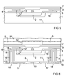
- Figure 1 is a cross section of an embodiment of the semiconductor device.
- a semiconductor substrate 1 comprising a main surface 10 and a back side 11 opposite the main surface 10 is penetrated by a through-substrate via 4, which electrically connects a contact area 16 of a metal layer 12, which is arranged above the main surface 10, with a contact pad 17 of a metal layer 15, which is arranged in the via hole 14 and on the back side 11.
- a sensor 2 especially an optical sensor like a photodetector, is arranged in the substrate 1 at the main surface 10.
- a filter 3 is arranged above the main surface 10 and above the sensor 2.
- the filter 3 may be formed by a single layer or by a layer sequence comprising two or more layers of different materials.
- a layer sequence may especially be provided as an interference filter.
- the substrate 1 may further comprise an integrated circuit, especially an integrated circuit for the operation of the sensor 2 and/or for the evaluation of measurements performed with the sensor 2, like a CMOS circuit, for instance.
- the metal layer 12 may be part of a wiring of the integrated circuit and may be embedded in a dielectric layer 6, 7, which may be silicon dioxide, for instance, and which serves as an intermetal dielectric.
- the structured metallization layers of the wiring may be interconnected by vertical interconnections 13, which can be formed by metal plugs, for instance.
- the passivation layer 9 may be a silicon nitride, for instance.
- the passivation layer 9 is preferably provided with an opening 20 above the sensor 2 to prevent the incident radiation from being adversely affected by the material of the passivation layer 9. In particular, variations of the intensity of the incoming light, which depend on the wavelength and may be caused by the material of the passivation layer 9, are thus avoided.
- the frame layer 5 may encompass the filter 3, but this is not necessarily the case.
- the frame layer 5 may instead be confined to a region above the through-substrate via 4. Thus the thin membrane formed at the bottom of the through-substrate via 4 by the dielectric layer 6, 7 and the metal layer 12 comprising the contact area 16 can be reinforced by the frame layer 5.
- a further dielectric layer 8 may be provided to insulate the metal layer 15 of the through-substrate via 4 from the semiconductor material of the substrate 1.
- the passivation layer 19 is open above the contact pads 17, where solder balls 18 or similar contacts may be placed for external electrical connection.
- the volume of the via hole 14 that is not filled with the metal layer 15 can be left open, or it can be filled with further electrically conductive material and/or with a dielectric material, especially the material of the passivation layer 19.
- Figure 2 is a cross section of a further embodiment of the semiconductor device.
- the elements of the embodiment according to Figure 2 that are similar to corresponding elements of the embodiment according to Figure 1 are designated with the same reference numerals.
- the embodiment according to Figure 2 does not comprise a gap between the filter 3 and the frame layer 5.
- the filter 3 and the frame layer 5 are arranged on the same plane formed by the upper surface of the dielectric layer 6, 7.
- Figure 3 shows a cross section of the semiconductor substrate 1, which may be a CMOS wafer at a stage after processing of the integrated circuitry, for instance.
- the CMOS wafer is provided with a plurality of sensors 2 and appertaining integrated circuits, each being provided for a single semiconductor chip.
- a corresponding plurality of through-substrate vias is produced for an electrical connection of the terminals.
- the production process will be described in conjunction with one sensor 2, one appertaining filter 3 and a through-substrate via 4 by way of example.
- An additional dielectric layer 7, which may be a silicon oxide, for instance, may be deposited on the passivation layer 9. The surface is then planarised, preferably by CMP (chemical mechanical polishing), so that a spatial variation of its level above the substrate 1 may only occur within a sufficiently small range of at most 10 nm.
- CMP chemical mechanical polishing
- the filter 3 can be produced by forming a patterned lift-off mask, which may be a resist, for instance, then sputtering or evaporating suitable filter layers, and subsequently performing a wet-chemical lift-off step to remove the lift-off mask and, together with the mask, the portion of the filter layers that are applied on the lift-off mask.
- the filter 3 can be formed by applying an entire layer or layer sequence on the planarized surface and removing the filter layer or layer sequence from areas outside the area above the sensor 2.
- the step 27 indicated in Figure 3 may be formed in the upper dielectric layer 7 at the edge of the filter 3.
- the step 27 does not adversely affect the performance of the device. If the passivation layer 9 is provided with an appropriate opening 20, only material of the dielectric layer 6, 7 is present between the sensor 2 and the filter 3.
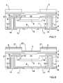
- Figure 4 is a cross section according to Figure 3 for a further intermediate product obtained after the application of a semiconductor body 24 on the upper surface of the dielectric layer 6, 7.
- the semiconductor body 24 may be silicon, for instance.
- the semiconductor body 24 comprises a recess 22, which can be formed by etching the surface of the semiconductor body 24, for instance.
- the semiconductor body 24 is arranged with the recess 22 facing the sensor 2, so that the filter 3 is accomodated in the recess 22.
- the semiconductor body 24 may especially be a structured handling wafer, which is bonded to the CMOS wafer or substrate 1 comprising the sensor 2, and the arrangement may be facilitated by an optical alignment of structured patterns on the surfaces of both wafers.
- the dielectric layer 6, 7 may serve as a bonding layer.
- the diameter of the CMOS wafer is preferably about 0.5 mm smaller than the diameter of the handling wafer to ensure that the edge of the CMOS wafer is not damaged during subsequent process steps.
- the semiconductor body 24 may have a thickness of typically about 725 ⁇ m, for example.
- the recess 22 may have a depth of typically about 40 ⁇ m, for example.
- the CMOS wafer is preferably thinned from the back side 11 by grinding and polishing to a thickness of 200 ⁇ m or less.
- the semiconductor body 24 serves as a handling wafer and improves the mechanical stability of the thinned substrate 1 during the subsequent production of the through-substrate via 4.
- a suitable process for producing the through-substrate via 4 begins with a formation of structures on the back side 11 in order to aid an alignment with structures already present at the main surface 10.
- a masked etching step is performed from the back side 11 to produce a via hole 14 penetrating the substrate 1.
- the dielectric layer 8 can be formed by a deposition of a dielectric material, by an oxidation of the surface of the semiconductor material or by an insulating implantation into the semiconductor material, for example.
- a silicon oxide covering the side wall of the via hole 14 may be deposited, and an anisotropic spacer etching step subsequently performed may uncover the contact area 16 at the bottom of the via hole 14 while leaving the side wall of the via hole 14 coated with the oxide.
- a barrier layer which may comprise titanium nitride or tantalum nitride, for instance, is deposited on the side wall of the via hole 14, and a metal layer, which may be tungsten, for example, is deposited on the barrier layer.
- the tungsten layer is then anisotropically etched, so that the side wall of the via hole 14 remains covered with tungsten.
- a suitable metal like aluminum is then sputtered on the back side 11. An area where the tungsten layer and the aluminum layer overlap ensures a low-ohmic connection between the tungsten and aluminum layers.
- the metal layer 15 is produced, which comprises a portion located within the via hole 14 and a portion located on the back side 11.
- the metal layer 15 may instead be formed from one entire layer, which is deposited both inside and outside the via hole 14.
- the metal layer 15 is preferably structured on the back side 11, so that contact pads 17 are provided.
- the remaining volume of the via hole 14 may be filled with an electrically conductive material like copper or with a dielectric.
- the process steps forming the through-substrate via 4 can generally be performed according to the prior art cited above.
- the semiconductor body 24 is ground from the side opposite the substrate 1. This process step may be facilitated if a grinding foil is laminated above the back side 11, especially on the passivation layer 19. The use of such a foil is known per se, and the foil is not shown in Figure 4 .
- the semiconductor body 24 is thinned at least until the recess 22 is reached and thus opened without causing damage to the filter 3.
- the residual thickness of the semiconductor body 24 may be typically about 20 ⁇ m, for example.
- the position of the upper surface of the thinned semiconductor body 24 is indicated in Figure 3 by the horizontal broken line.
- the remaining portion of the semiconductor body 24 forms the frame layer 5, which covers and reinforces a device area including the bottom of the through-substrate via 4. Thereby formation of cracks in the thin membrane formed by the layers remaining above the through-substrate via 4 is reliably prevented.
- the filter is not formed before the semiconductor body 24 is applied.
- Figure 5 is a cross section according to Figure 3 , which represents a process stage at the end of the CMOS process. Corresponding elements are designated with the same reference numerals.
- the planar upper dielectric layer 7 is not yet provided with any filter layer.
- Figure 6 is a cross section according to Figure 5 for a further intermediate product obtained after the application of a semiconductor body 24, which comprises a recess 22, on the upper surface of the dielectric layer 6, 7.
- the semiconductor body 24 may be silicon, for instance.
- the semiconductor body 24 is arranged with the recess 22 facing the sensor 2.
- the semiconductor body 24 may especially be a structured handling wafer, which is bonded to the CMOS wafer, and the dielectric layer 6, 7 may serve as a bonding layer.
- the diameter of the CMOS wafer is preferably about 0.5 mm smaller than the diameter of the handling wafer to ensure that the edge of the CMOS wafer is not damaged during subsequent process steps.
- the semiconductor body 24 may have a thickness of typically about 725 ⁇ m, and the recess 22 may have a depth of typically about 40 ⁇ m, for example.
- the thinning of the substrate 1 and the formation of the through-substrate via 4 may then take place as described above. Then the semiconductor body 24 is ground from the side opposite the substrate 1 at least until the recess 22 is reached and opened.
- the location of the upper surface of the thinned semiconductor body 24 is indicated in Figure 6 by the horizontal broken line. The remaining portion of the semiconductor body 24 forms the frame layer 5.
- Figure 7 is a cross section according to Figure 6 for a further intermediate product obtained after the semiconductor body 24 has been thinned from the side opposite the substrate 1 until the recess 22 is opened and an area of the dielectric layer 7 above the sensor 2 is exposed.
- the frame layer 5 covers the area of the through-substrate via 4.
- Figure 8 is a cross section according to Figure 7 after the application of a sacrificial layer 21 on the frame layer 5.
- the sacrificial layer 21 may be a dry film resist, for instance.
- the sacrificial layer 21 is preferably confined to the surface of the frame layer 5, but a small overlap of the sacrificial layer 21 into the opening of the frame layer 5 above the sensor 2 does no harm.
- an entire filter layer or sequence of filter layers 23 is applied, especially by sputtering, for example. Because of the step formed by the perimeter of the opening in the frame layer 5 and the restricted conformity of the edge coverage obtained by the sputtering process, the filter layer or sequence of filter layers 23 may not perfectly cover the perimeter of the opening that is present in the frame layer 5.
- the sacrificial layer 21 and the portion of the filter layer or sequence of filter layers 23 that is applied on the sacrificial layer 21 are removed by a lift-off process, in particular by a wet-chemical lift-off process.
- the remaining portion of the filter layer or sequence of filter layers 23 forms the filter 3 above the sensor 2.
- Figure 9 is a cross section according to Figure 6 for a further variant of the production method using a semiconductor body 25 without recess.
- the semiconductor body 25 may be an unstructured handling wafer, for instance.
- the back side 11 of the substrate 1 is temporarily bonded to a handling wafer 26.
- the passivation layer 19 may be used as a bonding layer, as shown in Figure 9 , or a dedicated bonding layer of silicon oxide, for instance, may be applied.
- the semiconductor body 25 is ground and polished to a thickness of typically about 20 ⁇ m as described above. The location of the upper surface of the thinned semiconductor body 25 is indicated in Figure 9 by the horizontal broken line.
- Figure 10 is a cross section according to Figure 9 after the semiconductor body 25 has been thinned.
- a mask 28 that is open in the area above the sensor 2 is applied on the surface of the remaining portion of the semiconductor body 25.
- the mask 28 may be a resist, which can be patterned by an infrared alignment step, for example.
- the mask 28 is then used for partially removing the semiconductor body 25 by etching, in particular by a dry chemical etching step having a high selectivity to the material of the dielectric layer 6, 7, which may be silicon oxide, for example.
- the portion of the semiconductor body 25 that is covered by the mask 28 remains as the frame layer 5 and covers at least the area above the through-substrate via 4.
- the mask 28 is removed, so that an intermediate product similar to the one shown in Figure 7 is obtained.
- the filter 3 is formed by further method steps according to the method steps described above in conjunction with Figure 8 .
- the handling wafer 26 is removed, and the embodiment according to Figure 2 is thus obtained.
- Further method steps that may be applied similarly for all embodiments described may include coating the contact pads 27 with nickel and gold by an electroless deposition to form an under-bump metallization, and attaching solder balls 18 to the under-bump metallization with a thermal reflow effected subsequently.
- the sawing of the wafer into single chips can be done with a dual-cut process, for example. The wafer is first sawn from the main surface 10, the CMOS side, without severing the substrate 1, and then completely cut from the back side 11.
- the application of the frame layer 5 described provides a highly reliable chip scale package especially for optical applications including interconnections formed by through-substrate vias.
- the method of producing the semiconductor device is compatible with a standard CMOS process. With this method it is possible to manufacture very thin chip scale packages, whose height is typically smaller than about 270 ⁇ m, hence substantially smaller than the height of semiconductor devices for optical applications according to the prior art. This offers considerable advantages in system integration, especially for consumer products.
- the reliability and mechanical stability of the membranes formed at the bottom of the through-substrate vias are substantially improved.
Landscapes
- Solid State Image Pick-Up Elements (AREA)
- Internal Circuitry In Semiconductor Integrated Circuit Devices (AREA)
- Light Receiving Elements (AREA)
Abstract
Description
-
US 2007/249095 A1 discloses a semiconductor package including an infrared filter bonded to a wafer. A suitable infrared filter layer is applied on a glass sheet having the same dimensions as the wafer. The glass sheet is bonded to the wafer with the filter layer facing towards the wafer, which is subsequently thinned. The resulting total thickness of the wafer and the filter is not greater than the initial thickness of the wafer. Via holes are formed through the wafer from the side opposite the filter to contact pad electrodes that are located between the wafer and the filter. -
DE 102009004725 A1 describes stacked semiconductor devices with a bond layer including a buried contact pad, which is connected with a metal layer on the upper surface of one of the wafers by means of a metallization in a through-wafer via. The contact pad and the surface metal layer can be connected with a metal plane of a wiring or with a contact pad that is provided for a connection with a further semiconductor device. - The formation of through-silicon vias in a semiconductor substrate is described in
US 8,378,496 B2 ,WO 2010/006916 A1 andWO 2011/039167 A1 . - Production methods using temporary bonding are described in
US 2005/0173064 A1 ,US 2009/0218560 A1 ,DE 10156465 C1 andWO 2013/056936 A1 . - It is an object of the present invention to disclose a highly reliable semiconductor chip scale package for optical applications and a method of producing such a semiconductor chip scale package.
- This object is achieved with the semiconductor device according to
claim 1 and with the method of producing a semiconductor device according toclaim 7. Embodiments and variants derive from the dependent claims. - The semiconductor device comprises a semiconductor substrate with a main surface, a sensor arranged in the substrate at the main surface, a filter arranged above the sensor, and a through-substrate via penetrating the substrate outside the sensor. A frame layer is arranged above the main surface above the through-substrate via. The frame layer does not cover the filter, which is on a level with the frame layer.
- In particular, the frame layer may be a silicon layer. The sensor may be an optical sensor, and the filter may be an optical filter, especially an interference filter, which may especially be used as an ultraviolet and/or infrared cut-off filter, a photopic filter, a colour filter, a band pass filter or any combination thereof.
- Further embodiments comprise a dielectric layer on the main surface, the filter and the frame layer being arranged on the dielectric layer.
- Further embodiments comprise a metal layer arranged in the dielectric layer, a contact area of the metal layer between the through-substrate via and the frame layer, and a metal layer of the through-substrate via contacting the contact area.
- Further embodiments comprise a passivation layer arranged in the dielectric layer. The passivation layer comprises a material different from the dielectric layer and an opening between the sensor and the filter.
- The method of producing a semiconductor device comprises arranging a sensor at a main surface of a semiconductor substrate, arranging a filter above the sensor, and forming a through-substrate via penetrating the substrate outside the sensor. A semiconductor body is applied above the main surface and then partially removed at least in an area above the sensor. A portion of the semiconductor body remains above the through-substrate via.
- In a variant of the method, the semiconductor body is provided with a recess and applied with the recess facing the sensor. The semiconductor body is thinned from a side opposite the substrate, until the recess is reached and the area above the sensor is thus uncovered.
- In a further variant of the method, the filter is arranged above the sensor before the semiconductor body is applied, and the semiconductor body is applied with the recess facing the sensor such that the filter is accomodated in the recess.
- In a further variant of the method, the filter is arranged above the sensor after the semiconductor body has partially been removed.
- In a further variant of the method, a mask is applied after applying and before partially removing the semiconductor body. The mask is open in the area above the sensor and used for partially removing the semiconductor body by etching, the portion remaining above the through-substrate via being covered by the mask.
- In a further variant of the method, a sacrificial layer is applied on the portion of the semiconductor body remaining above the through-substrate via, a filter layer is applied on the sacrificial layer and the area above the sensor, and the sacrificial layer is removed together with a portion of the filter layer, so that a remaining portion of the filter layer forms the filter.
- The following is a detailed description of examples of the semiconductor device and the production method in conjunction with the appended figures.
- Figure 1
- is a cross section of an embodiment of the semiconductor device.
- Figure 2
- is a cross section of a further embodiment of the semiconductor device.
- Figure 3
- is a cross section of an intermediate product of a variant of the production method.
- Figure 4
- is a cross section according to
Figure 3 after the formation of through-substrate vias. - Figure 5
- is a cross section of an intermediate product of a further variant of the production method.
- Figure 6
- is a cross section according to
Figure 5 after the formation of through-substrate vias. - Figure 7
- is a cross section according to
Figure 6 after the frame layer has been formed. - Figure 8
- is a cross section according to
Figure 7 after the application of filter layers. - Figure 9
- is a cross section according to
Figure 6 for a further variant of the production method. - Figure 10
- is a cross section according to
Figure 9 after the application of a mask to form the frame layer. -
Figure 1 is a cross section of an embodiment of the semiconductor device. Asemiconductor substrate 1 comprising amain surface 10 and aback side 11 opposite themain surface 10 is penetrated by a through-substrate via 4, which electrically connects acontact area 16 of ametal layer 12, which is arranged above themain surface 10, with acontact pad 17 of ametal layer 15, which is arranged in thevia hole 14 and on theback side 11. Asensor 2, especially an optical sensor like a photodetector, is arranged in thesubstrate 1 at themain surface 10. Afilter 3 is arranged above themain surface 10 and above thesensor 2. Thefilter 3 may be formed by a single layer or by a layer sequence comprising two or more layers of different materials. A layer sequence may especially be provided as an interference filter. - The
substrate 1 may further comprise an integrated circuit, especially an integrated circuit for the operation of thesensor 2 and/or for the evaluation of measurements performed with thesensor 2, like a CMOS circuit, for instance. Themetal layer 12 may be part of a wiring of the integrated circuit and may be embedded in adielectric layer vertical interconnections 13, which can be formed by metal plugs, for instance. - A
passivation layer 9, which comprises a material that is different from the dielectric material of thedielectric layer metal layers 12 of the wiring, especially between the intermetaldielectric layer 6 and an upper portion of thedielectric layer 7. If thedielectric layer passivation layer 9 may be a silicon nitride, for instance. Thepassivation layer 9 is preferably provided with an opening 20 above thesensor 2 to prevent the incident radiation from being adversely affected by the material of thepassivation layer 9. In particular, variations of the intensity of the incoming light, which depend on the wavelength and may be caused by the material of thepassivation layer 9, are thus avoided. - A
frame layer 5, which may be silicon, for example, is arranged on thedielectric layer filter 3. A small gap may be present between thefilter 3 and theframe layer 5. This is indicated inFigure 1 . Theframe layer 5 may encompass thefilter 3, but this is not necessarily the case. Theframe layer 5 may instead be confined to a region above the through-substrate via 4. Thus the thin membrane formed at the bottom of the through-substrate via 4 by thedielectric layer metal layer 12 comprising thecontact area 16 can be reinforced by theframe layer 5. - On the
back side 11, afurther dielectric layer 8 may be provided to insulate themetal layer 15 of the through-substrate via 4 from the semiconductor material of thesubstrate 1. Apassivation layer 19, which may comprise a silicon oxide and/or a silicon nitride, for instance, may be provided to cover theback side 11. Thepassivation layer 19 is open above thecontact pads 17, wheresolder balls 18 or similar contacts may be placed for external electrical connection. The volume of the viahole 14 that is not filled with themetal layer 15 can be left open, or it can be filled with further electrically conductive material and/or with a dielectric material, especially the material of thepassivation layer 19. -
Figure 2 is a cross section of a further embodiment of the semiconductor device. The elements of the embodiment according toFigure 2 that are similar to corresponding elements of the embodiment according toFigure 1 are designated with the same reference numerals. The embodiment according toFigure 2 does not comprise a gap between thefilter 3 and theframe layer 5. Furthermore, thefilter 3 and theframe layer 5 are arranged on the same plane formed by the upper surface of thedielectric layer - Methods of producing the semiconductor device will be described in the following in conjunction with
Figures 3 to 10 , which show cross sections of intermediate products. The elements that are similar to corresponding elements of the embodiments according toFigures 1 and 2 are designated with the same reference numerals. -
Figure 3 shows a cross section of thesemiconductor substrate 1, which may be a CMOS wafer at a stage after processing of the integrated circuitry, for instance. In the desired chip scale package, the CMOS wafer is provided with a plurality ofsensors 2 and appertaining integrated circuits, each being provided for a single semiconductor chip. A corresponding plurality of through-substrate vias is produced for an electrical connection of the terminals. The production process will be described in conjunction with onesensor 2, one appertainingfilter 3 and a through-substrate via 4 by way of example. - A
passivation layer 9, which may comprise silicon nitride, for instance, may be provided on thedielectric layer 6 of the wiring. Such apassivation layer 9 is preferably opened above thesensor 2, in particular by masked plasma etching, for instance. An additionaldielectric layer 7, which may be a silicon oxide, for instance, may be deposited on thepassivation layer 9. The surface is then planarised, preferably by CMP (chemical mechanical polishing), so that a spatial variation of its level above thesubstrate 1 may only occur within a sufficiently small range of at most 10 nm. - The
filter 3, which may be formed by structured interference filter layers, for instance, is applied on the planarised surface above the area of thesensor 2. In particular, thefilter 3 can be produced by forming a patterned lift-off mask, which may be a resist, for instance, then sputtering or evaporating suitable filter layers, and subsequently performing a wet-chemical lift-off step to remove the lift-off mask and, together with the mask, the portion of the filter layers that are applied on the lift-off mask. Instead, thefilter 3 can be formed by applying an entire layer or layer sequence on the planarized surface and removing the filter layer or layer sequence from areas outside the area above thesensor 2. If the filter layer or layer sequence is etched, thestep 27 indicated inFigure 3 may be formed in theupper dielectric layer 7 at the edge of thefilter 3. Thestep 27 does not adversely affect the performance of the device. If thepassivation layer 9 is provided with anappropriate opening 20, only material of thedielectric layer sensor 2 and thefilter 3. -
Figure 4 is a cross section according toFigure 3 for a further intermediate product obtained after the application of asemiconductor body 24 on the upper surface of thedielectric layer semiconductor body 24 may be silicon, for instance. In this variant of the method, thesemiconductor body 24 comprises arecess 22, which can be formed by etching the surface of thesemiconductor body 24, for instance. Thesemiconductor body 24 is arranged with therecess 22 facing thesensor 2, so that thefilter 3 is accomodated in therecess 22. Thesemiconductor body 24 may especially be a structured handling wafer, which is bonded to the CMOS wafer orsubstrate 1 comprising thesensor 2, and the arrangement may be facilitated by an optical alignment of structured patterns on the surfaces of both wafers. Thedielectric layer semiconductor body 24 may have a thickness of typically about 725 µm, for example. Therecess 22 may have a depth of typically about 40 µm, for example. - The CMOS wafer is preferably thinned from the
back side 11 by grinding and polishing to a thickness of 200 µm or less. Thesemiconductor body 24 serves as a handling wafer and improves the mechanical stability of the thinnedsubstrate 1 during the subsequent production of the through-substrate via 4. - A suitable process for producing the through-substrate via 4 begins with a formation of structures on the
back side 11 in order to aid an alignment with structures already present at themain surface 10. In accordance with these structures, a masked etching step is performed from theback side 11 to produce a viahole 14 penetrating thesubstrate 1. Thedielectric layer 8 can be formed by a deposition of a dielectric material, by an oxidation of the surface of the semiconductor material or by an insulating implantation into the semiconductor material, for example. In particular, a silicon oxide covering the side wall of the viahole 14 may be deposited, and an anisotropic spacer etching step subsequently performed may uncover thecontact area 16 at the bottom of the viahole 14 while leaving the side wall of the viahole 14 coated with the oxide. - Then a barrier layer, which may comprise titanium nitride or tantalum nitride, for instance, is deposited on the side wall of the via
hole 14, and a metal layer, which may be tungsten, for example, is deposited on the barrier layer. The tungsten layer is then anisotropically etched, so that the side wall of the viahole 14 remains covered with tungsten. A suitable metal like aluminum is then sputtered on theback side 11. An area where the tungsten layer and the aluminum layer overlap ensures a low-ohmic connection between the tungsten and aluminum layers. Thus themetal layer 15 is produced, which comprises a portion located within the viahole 14 and a portion located on theback side 11. Themetal layer 15 may instead be formed from one entire layer, which is deposited both inside and outside the viahole 14. Themetal layer 15 is preferably structured on theback side 11, so thatcontact pads 17 are provided. - The remaining volume of the via
hole 14 may be filled with an electrically conductive material like copper or with a dielectric. Apassivation layer 19, which may comprise silicon oxide and/or silicon nitride, can be applied and opened above thecontact pads 17. In the embodiment shown inFigure 4 , thepassivation layer 19 is also applied on themetal layer 15 inside the viahole 14. The process steps forming the through-substrate via 4 can generally be performed according to the prior art cited above. - After the formation of the through-substrate via 4 and the structuring of the
metal layer 15 on theback side 11, thesemiconductor body 24 is ground from the side opposite thesubstrate 1. This process step may be facilitated if a grinding foil is laminated above theback side 11, especially on thepassivation layer 19. The use of such a foil is known per se, and the foil is not shown inFigure 4 . Thesemiconductor body 24 is thinned at least until therecess 22 is reached and thus opened without causing damage to thefilter 3. The residual thickness of thesemiconductor body 24 may be typically about 20 µm, for example. The position of the upper surface of the thinnedsemiconductor body 24 is indicated inFigure 3 by the horizontal broken line. - The remaining portion of the
semiconductor body 24 forms theframe layer 5, which covers and reinforces a device area including the bottom of the through-substrate via 4. Thereby formation of cracks in the thin membrane formed by the layers remaining above the through-substrate via 4 is reliably prevented. After the application of solder balls on thecontact pads 17, the embodiment according toFigure 1 is obtained. - In a further variant of the method, the filter is not formed before the
semiconductor body 24 is applied.Figure 5 is a cross section according toFigure 3 , which represents a process stage at the end of the CMOS process. Corresponding elements are designated with the same reference numerals. In the intermediate product shown inFigure 5 , the planarupper dielectric layer 7 is not yet provided with any filter layer. -
Figure 6 is a cross section according toFigure 5 for a further intermediate product obtained after the application of asemiconductor body 24, which comprises arecess 22, on the upper surface of thedielectric layer semiconductor body 24 may be silicon, for instance. As in the variant of the method previously described, thesemiconductor body 24 is arranged with therecess 22 facing thesensor 2. Thesemiconductor body 24 may especially be a structured handling wafer, which is bonded to the CMOS wafer, and thedielectric layer semiconductor body 24 may have a thickness of typically about 725 µm, and therecess 22 may have a depth of typically about 40 µm, for example. The thinning of thesubstrate 1 and the formation of the through-substrate via 4 may then take place as described above. Then thesemiconductor body 24 is ground from the side opposite thesubstrate 1 at least until therecess 22 is reached and opened. The location of the upper surface of the thinnedsemiconductor body 24 is indicated inFigure 6 by the horizontal broken line. The remaining portion of thesemiconductor body 24 forms theframe layer 5. -
Figure 7 is a cross section according toFigure 6 for a further intermediate product obtained after thesemiconductor body 24 has been thinned from the side opposite thesubstrate 1 until therecess 22 is opened and an area of thedielectric layer 7 above thesensor 2 is exposed. Theframe layer 5 covers the area of the through-substrate via 4. -
Figure 8 is a cross section according toFigure 7 after the application of asacrificial layer 21 on theframe layer 5. Thesacrificial layer 21 may be a dry film resist, for instance. Thesacrificial layer 21 is preferably confined to the surface of theframe layer 5, but a small overlap of thesacrificial layer 21 into the opening of theframe layer 5 above thesensor 2 does no harm. Then an entire filter layer or sequence of filter layers 23 is applied, especially by sputtering, for example. Because of the step formed by the perimeter of the opening in theframe layer 5 and the restricted conformity of the edge coverage obtained by the sputtering process, the filter layer or sequence of filter layers 23 may not perfectly cover the perimeter of the opening that is present in theframe layer 5. In a subsequent step, thesacrificial layer 21 and the portion of the filter layer or sequence of filter layers 23 that is applied on thesacrificial layer 21 are removed by a lift-off process, in particular by a wet-chemical lift-off process. The remaining portion of the filter layer or sequence of filter layers 23 forms thefilter 3 above thesensor 2. After the application of solder balls on thecontact pads 17, the embodiment according toFigure 2 is obtained. -
Figure 9 is a cross section according toFigure 6 for a further variant of the production method using asemiconductor body 25 without recess. Thesemiconductor body 25 may be an unstructured handling wafer, for instance. After the formation of the through-substrate via 4, theback side 11 of thesubstrate 1 is temporarily bonded to a handlingwafer 26. For this purpose, thepassivation layer 19 may be used as a bonding layer, as shown inFigure 9 , or a dedicated bonding layer of silicon oxide, for instance, may be applied. Thesemiconductor body 25 is ground and polished to a thickness of typically about 20 µm as described above. The location of the upper surface of the thinnedsemiconductor body 25 is indicated inFigure 9 by the horizontal broken line. -
Figure 10 is a cross section according toFigure 9 after thesemiconductor body 25 has been thinned. Amask 28 that is open in the area above thesensor 2 is applied on the surface of the remaining portion of thesemiconductor body 25. Themask 28 may be a resist, which can be patterned by an infrared alignment step, for example. Themask 28 is then used for partially removing thesemiconductor body 25 by etching, in particular by a dry chemical etching step having a high selectivity to the material of thedielectric layer semiconductor body 25 that is covered by themask 28 remains as theframe layer 5 and covers at least the area above the through-substrate via 4. Themask 28 is removed, so that an intermediate product similar to the one shown inFigure 7 is obtained. Then thefilter 3 is formed by further method steps according to the method steps described above in conjunction withFigure 8 . The handlingwafer 26 is removed, and the embodiment according toFigure 2 is thus obtained. - Further method steps that may be applied similarly for all embodiments described may include coating the
contact pads 27 with nickel and gold by an electroless deposition to form an under-bump metallization, and attachingsolder balls 18 to the under-bump metallization with a thermal reflow effected subsequently. The sawing of the wafer into single chips can be done with a dual-cut process, for example. The wafer is first sawn from themain surface 10, the CMOS side, without severing thesubstrate 1, and then completely cut from theback side 11. - The application of the
frame layer 5 described provides a highly reliable chip scale package especially for optical applications including interconnections formed by through-substrate vias. The method of producing the semiconductor device is compatible with a standard CMOS process. With this method it is possible to manufacture very thin chip scale packages, whose height is typically smaller than about 270 µm, hence substantially smaller than the height of semiconductor devices for optical applications according to the prior art. This offers considerable advantages in system integration, especially for consumer products. The reliability and mechanical stability of the membranes formed at the bottom of the through-substrate vias are substantially improved. -
- 1
- semiconductor substrate
- 2
- sensor
- 3
- filter
- 4
- through-substrate via
- 5
- frame layer
- 6
- dielectric layer
- 7
- dielectric layer
- 8
- dielectric layer
- 9
- passivation layer
- 10
- main surface
- 11
- back side
- 12
- metal layer
- 13
- interconnection
- 14
- via hole
- 15
- metal layer
- 16
- contact area
- 17
- contact pad
- 18
- solder ball
- 19
- passivation layer
- 20
- opening
- 21
- sacrificial layer
- 22
- recess
- 23
- filter layer
- 24
- semiconductor body with recess
- 25
- semiconductor body without recess
- 26
- handling wafer
- 27
- step
- 28
- mask
Claims (12)
- A semiconductor device, comprising:- a semiconductor substrate (1) with a main surface (10),- a sensor (2) arranged in the substrate (1) at the main surface (10),- a filter (3) arranged above the sensor (2), and- a through-substrate via (4) penetrating the substrate (1) outside the sensor (2),
characterized in that- a frame layer (5) is arranged above the main surface (10) above the through-substrate via (4),- the frame layer (5) does not cover the filter (3), and- the filter (3) is on a level with the frame layer (5). - The semiconductor device of claim 1, wherein the frame layer (5) is a silicon layer.
- The semiconductor device of claim 1 or 2, further comprising:a dielectric layer (6, 7) on the main surface (10), the filter (3) and the frame layer (5) being arranged on the dielectric layer (6, 7).
- The semiconductor device of claim 3, further comprising:a metal layer (12) arranged in the dielectric layer (6, 7),a contact area (16) of the metal layer (12) between the through-substrate via (4) and the frame layer (5), anda metal layer (15) of the through-substrate via (4) contacting the contact area (16).
- The semiconductor device of claim 3 or 4, further comprising:a passivation layer (9) arranged in the dielectric layer (6, 7), comprising a material different from the dielectric layer (6, 7), and comprising an opening (20) between the sensor (2) and the filter (3).
- The semiconductor device of one of claims 1 to 5, wherein the sensor (2) is an optical sensor and the filter (3) is an optical filter.
- A method of producing a semiconductor device, comprising:- arranging a sensor (2) at a main surface (10) of a semiconductor substrate (1),- arranging a filter (3) above the sensor (2), and- forming a through-substrate via (4) penetrating the substrate (1) outside the sensor (2),
characterized in that- a semiconductor body (24, 25) is applied above the main surface (10), and- the semiconductor body (24, 25) is partially removed at least in an area above the sensor (2), a portion (5) of the semiconductor body (24, 25) remaining above the through-substrate via (4). - The method of claim 7, further comprising:- providing the semiconductor body (24) with a recess (22),- applying the semiconductor body (24) with the recess (22) facing the sensor (2), and- thinning the semiconductor body (24) from a side opposite the substrate (1) until the recess (22) is reached and the area above the sensor (2) is uncovered.
- The method of claim 8, further comprising:- arranging the filter (3) above the sensor (2) before the semiconductor body (24) is applied, and- applying the semiconductor body (24) with the recess (22) facing the sensor (2) such that the filter (3) is accomodated in the recess (22).
- The method of claim 7, wherein the filter (3) is arranged above the sensor (2) after the semiconductor body (24, 25) has partially been removed.
- The method of claim 10, further comprising:- after applying and before partially removing the semiconductor body (25), applying a mask (28) that is open in the area above the sensor (2), and- using the mask (28) for partially removing the semiconductor body (25) by etching, the portion (5) remaining above the through-substrate via (4) being covered by the mask (28).
- The method of claim 10 or 11, further comprising:- applying a sacrificial layer (21) on the portion (5) of the semiconductor body (25) remaining above the through-substrate via (4),- applying a filter layer (23) on the sacrificial layer (21) and the area above the sensor (2), and- removing the sacrificial layer (21) together with a portion of the filter layer (23), a remaining portion of the filter layer (23) forming the filter (3).
Priority Applications (4)
| Application Number | Priority Date | Filing Date | Title |
|---|---|---|---|
| EP14152688.9A EP2899760B1 (en) | 2014-01-27 | 2014-01-27 | Semiconductor device for optical applications and method of producing such a semiconductor device |
| US15/114,387 US10084004B2 (en) | 2014-01-27 | 2015-01-14 | Semiconductor device for optical applications and method of producing such a semiconductor device |
| PCT/EP2015/050587 WO2015110332A1 (en) | 2014-01-27 | 2015-01-14 | Semiconductor device for optical applications and method of producing such a semiconductor device |
| CN201580004240.1A CN105900247B (en) | 2014-01-27 | 2015-01-14 | Semiconductor device for optical applications and method of manufacturing such semiconductor device |
Applications Claiming Priority (1)
| Application Number | Priority Date | Filing Date | Title |
|---|---|---|---|
| EP14152688.9A EP2899760B1 (en) | 2014-01-27 | 2014-01-27 | Semiconductor device for optical applications and method of producing such a semiconductor device |
Publications (2)
| Publication Number | Publication Date |
|---|---|
| EP2899760A1 true EP2899760A1 (en) | 2015-07-29 |
| EP2899760B1 EP2899760B1 (en) | 2018-08-29 |
Family
ID=50002574
Family Applications (1)
| Application Number | Title | Priority Date | Filing Date |
|---|---|---|---|
| EP14152688.9A Active EP2899760B1 (en) | 2014-01-27 | 2014-01-27 | Semiconductor device for optical applications and method of producing such a semiconductor device |
Country Status (4)
| Country | Link |
|---|---|
| US (1) | US10084004B2 (en) |
| EP (1) | EP2899760B1 (en) |
| CN (1) | CN105900247B (en) |
| WO (1) | WO2015110332A1 (en) |
Families Citing this family (5)
| Publication number | Priority date | Publication date | Assignee | Title |
|---|---|---|---|---|
| CN106793931A (en) * | 2014-10-10 | 2017-05-31 | 奥林巴斯株式会社 | Light supply apparatus |
| EP3301072B1 (en) * | 2016-09-30 | 2024-02-21 | Sciosense B.V. | Semiconductor device and method for forming a semiconductor device |
| KR102399356B1 (en) * | 2017-03-10 | 2022-05-19 | 삼성전자주식회사 | Substrate, method of sawing substrate, and semiconductor device |
| US12426391B2 (en) * | 2021-04-30 | 2025-09-23 | Spectricity | Hyperspectral filter structure and method of manufacture |
| DE102024200633A1 (en) | 2024-01-24 | 2025-07-24 | Fraunhofer-Gesellschaft zur Förderung der angewandten Forschung eingetragener Verein | Vertical wiring of a semiconductor device |
Citations (3)
| Publication number | Priority date | Publication date | Assignee | Title |
|---|---|---|---|---|
| US20060035415A1 (en) * | 2004-08-16 | 2006-02-16 | Wood Alan G | Frame structure and semiconductor attach process for use therewith for fabrication of image sensor packages and the like, and resulting packages |
| US20110221018A1 (en) * | 2010-03-15 | 2011-09-15 | Xunqing Shi | Electronic Device Package and Methods of Manufacturing an Electronic Device Package |
| US20120091515A1 (en) * | 2010-10-13 | 2012-04-19 | Samsung Electronics Co., Ltd. | Semiconductor Devices Having Backside Illuminated Image Sensors |
Family Cites Families (14)
| Publication number | Priority date | Publication date | Assignee | Title |
|---|---|---|---|---|
| DE10156465C1 (en) | 2001-11-16 | 2003-07-10 | Infineon Technologies Ag | Bonded assembly of two wafers is formed using wafer recessed to make penetrations, and results in highly temperature-stable, detachable connection |
| JP2006135272A (en) | 2003-12-01 | 2006-05-25 | Tokyo Ohka Kogyo Co Ltd | Substrate support plate and support plate peeling method |
| KR20060087273A (en) | 2005-01-28 | 2006-08-02 | 삼성전기주식회사 | Semiconductor package and manufacturing method |
| US7964926B2 (en) * | 2005-02-02 | 2011-06-21 | Samsung Electronics Co., Ltd. | Image sensing devices including image sensor chips, image sensor package modules employing the image sensing devices, electronic products employing the image sensor package modules, and methods of fabricating the same |
| DE102007034306B3 (en) | 2007-07-24 | 2009-04-02 | Austriamicrosystems Ag | Semiconductor substrate with via and method for producing a semiconductor substrate with via |
| DE112009000140B4 (en) | 2008-01-24 | 2022-06-15 | Brewer Science, Inc. | Method for reversibly attaching a device wafer to a supporting substrate and an article obtained therefrom |
| DE102008033395B3 (en) | 2008-07-16 | 2010-02-04 | Austriamicrosystems Ag | Method for producing a semiconductor component and semiconductor component |
| DE102009004725A1 (en) | 2009-01-15 | 2010-07-29 | Austriamicrosystems Ag | Through-hole semiconductor circuit and method of manufacturing vertically integrated circuits |
| JP2011009645A (en) * | 2009-06-29 | 2011-01-13 | Toshiba Corp | Semiconductor device and method of manufacturing the same |
| KR20110003696A (en) * | 2009-07-06 | 2011-01-13 | 삼성전자주식회사 | Optical filter array for single chip stereoscopic image sensor and manufacturing method thereof |
| EP2306506B1 (en) | 2009-10-01 | 2013-07-31 | ams AG | Method of producing a semiconductor device having a through-wafer interconnect |
| DE102011116409B3 (en) | 2011-10-19 | 2013-03-07 | Austriamicrosystems Ag | Method for producing thin semiconductor components |
| US9324756B2 (en) * | 2012-07-25 | 2016-04-26 | Taiwan Semiconductor Manufacturing Company, Ltd. | CIS chips and methods for forming the same |
| JP2015032663A (en) * | 2013-08-01 | 2015-02-16 | 株式会社東芝 | Solid-state imaging device |
-
2014
- 2014-01-27 EP EP14152688.9A patent/EP2899760B1/en active Active
-
2015
- 2015-01-14 CN CN201580004240.1A patent/CN105900247B/en active Active
- 2015-01-14 WO PCT/EP2015/050587 patent/WO2015110332A1/en not_active Ceased
- 2015-01-14 US US15/114,387 patent/US10084004B2/en active Active
Patent Citations (3)
| Publication number | Priority date | Publication date | Assignee | Title |
|---|---|---|---|---|
| US20060035415A1 (en) * | 2004-08-16 | 2006-02-16 | Wood Alan G | Frame structure and semiconductor attach process for use therewith for fabrication of image sensor packages and the like, and resulting packages |
| US20110221018A1 (en) * | 2010-03-15 | 2011-09-15 | Xunqing Shi | Electronic Device Package and Methods of Manufacturing an Electronic Device Package |
| US20120091515A1 (en) * | 2010-10-13 | 2012-04-19 | Samsung Electronics Co., Ltd. | Semiconductor Devices Having Backside Illuminated Image Sensors |
Also Published As
| Publication number | Publication date |
|---|---|
| US20160343757A1 (en) | 2016-11-24 |
| CN105900247A (en) | 2016-08-24 |
| US10084004B2 (en) | 2018-09-25 |
| CN105900247B (en) | 2017-08-25 |
| EP2899760B1 (en) | 2018-08-29 |
| WO2015110332A1 (en) | 2015-07-30 |
Similar Documents
| Publication | Publication Date | Title |
|---|---|---|
| US10157811B2 (en) | Chip package and method for forming the same | |
| US10056419B2 (en) | Chip package having chip connected to sensing device with redistribution layer in insulator layer | |
| US10153237B2 (en) | Chip package and method for forming the same | |
| US8552565B2 (en) | Chip package and method for forming the same | |
| US11107848B2 (en) | Semiconductor device for detection of radiation and method of producing a semiconductor device for detection of radiation | |
| US9379072B2 (en) | Chip package and method for forming the same | |
| TWI628784B (en) | Stress release image sensor package structure and method | |
| US10109663B2 (en) | Chip package and method for forming the same | |
| US20160221819A1 (en) | Mems-cmos device that minimizes outgassing and methods of manufacture | |
| US10140498B2 (en) | Wafer-level packaging sensing device and method for forming the same | |
| US10084004B2 (en) | Semiconductor device for optical applications and method of producing such a semiconductor device | |
| US20170186712A1 (en) | Chip package and method for forming the same | |
| US9865526B2 (en) | Chip package and method for forming the same | |
| US20170053848A1 (en) | Sensing module and method for forming the same | |
| CN103579266A (en) | CIS chips and methods for forming same | |
| US20160325984A1 (en) | Chip scale package | |
| HK1234529A1 (en) | Stress released image sensor package structure and method | |
| HK1234529A (en) | Stress released image sensor package structure and method |
Legal Events
| Date | Code | Title | Description |
|---|---|---|---|
| PUAI | Public reference made under article 153(3) epc to a published international application that has entered the european phase |
Free format text: ORIGINAL CODE: 0009012 |
|
| 17P | Request for examination filed |
Effective date: 20140127 |
|
| AK | Designated contracting states |
Kind code of ref document: A1 Designated state(s): AL AT BE BG CH CY CZ DE DK EE ES FI FR GB GR HR HU IE IS IT LI LT LU LV MC MK MT NL NO PL PT RO RS SE SI SK SM TR |
|
| AX | Request for extension of the european patent |
Extension state: BA ME |
|
| 17P | Request for examination filed |
Effective date: 20151216 |
|
| RBV | Designated contracting states (corrected) |
Designated state(s): AL AT BE BG CH CY CZ DE DK EE ES FI FR GB GR HR HU IE IS IT LI LT LU LV MC MK MT NL NO PL PT RO RS SE SI SK SM TR |
|
| GRAP | Despatch of communication of intention to grant a patent |
Free format text: ORIGINAL CODE: EPIDOSNIGR1 |
|
| STAA | Information on the status of an ep patent application or granted ep patent |
Free format text: STATUS: GRANT OF PATENT IS INTENDED |
|
| RIC1 | Information provided on ipc code assigned before grant |
Ipc: H01L 27/146 20060101ALI20180201BHEP Ipc: H01L 31/0216 20140101ALI20180201BHEP Ipc: H01L 31/0203 20140101AFI20180201BHEP Ipc: H01L 23/48 20060101ALI20180201BHEP |
|
| INTG | Intention to grant announced |
Effective date: 20180307 |
|
| GRAS | Grant fee paid |
Free format text: ORIGINAL CODE: EPIDOSNIGR3 |
|
| GRAA | (expected) grant |
Free format text: ORIGINAL CODE: 0009210 |
|
| STAA | Information on the status of an ep patent application or granted ep patent |
Free format text: STATUS: THE PATENT HAS BEEN GRANTED |
|
| RAP1 | Party data changed (applicant data changed or rights of an application transferred) |
Owner name: AMS AG |
|
| AK | Designated contracting states |
Kind code of ref document: B1 Designated state(s): AL AT BE BG CH CY CZ DE DK EE ES FI FR GB GR HR HU IE IS IT LI LT LU LV MC MK MT NL NO PL PT RO RS SE SI SK SM TR |
|
| REG | Reference to a national code |
Ref country code: GB Ref legal event code: FG4D |
|
| REG | Reference to a national code |
Ref country code: CH Ref legal event code: EP |
|
| REG | Reference to a national code |
Ref country code: AT Ref legal event code: REF Ref document number: 1036168 Country of ref document: AT Kind code of ref document: T Effective date: 20180915 |
|
| REG | Reference to a national code |
Ref country code: IE Ref legal event code: FG4D |
|
| REG | Reference to a national code |
Ref country code: DE Ref legal event code: R096 Ref document number: 602014031182 Country of ref document: DE |
|
| RAP2 | Party data changed (patent owner data changed or rights of a patent transferred) |
Owner name: AMS AG |
|
| REG | Reference to a national code |
Ref country code: NL Ref legal event code: MP Effective date: 20180829 |
|
| REG | Reference to a national code |
Ref country code: LT Ref legal event code: MG4D |
|
| PG25 | Lapsed in a contracting state [announced via postgrant information from national office to epo] |
Ref country code: FI Free format text: LAPSE BECAUSE OF FAILURE TO SUBMIT A TRANSLATION OF THE DESCRIPTION OR TO PAY THE FEE WITHIN THE PRESCRIBED TIME-LIMIT Effective date: 20180829 Ref country code: RS Free format text: LAPSE BECAUSE OF FAILURE TO SUBMIT A TRANSLATION OF THE DESCRIPTION OR TO PAY THE FEE WITHIN THE PRESCRIBED TIME-LIMIT Effective date: 20180829 Ref country code: IS Free format text: LAPSE BECAUSE OF FAILURE TO SUBMIT A TRANSLATION OF THE DESCRIPTION OR TO PAY THE FEE WITHIN THE PRESCRIBED TIME-LIMIT Effective date: 20181229 Ref country code: SE Free format text: LAPSE BECAUSE OF FAILURE TO SUBMIT A TRANSLATION OF THE DESCRIPTION OR TO PAY THE FEE WITHIN THE PRESCRIBED TIME-LIMIT Effective date: 20180829 Ref country code: NO Free format text: LAPSE BECAUSE OF FAILURE TO SUBMIT A TRANSLATION OF THE DESCRIPTION OR TO PAY THE FEE WITHIN THE PRESCRIBED TIME-LIMIT Effective date: 20181129 Ref country code: NL Free format text: LAPSE BECAUSE OF FAILURE TO SUBMIT A TRANSLATION OF THE DESCRIPTION OR TO PAY THE FEE WITHIN THE PRESCRIBED TIME-LIMIT Effective date: 20180829 Ref country code: BG Free format text: LAPSE BECAUSE OF FAILURE TO SUBMIT A TRANSLATION OF THE DESCRIPTION OR TO PAY THE FEE WITHIN THE PRESCRIBED TIME-LIMIT Effective date: 20181129 Ref country code: GR Free format text: LAPSE BECAUSE OF FAILURE TO SUBMIT A TRANSLATION OF THE DESCRIPTION OR TO PAY THE FEE WITHIN THE PRESCRIBED TIME-LIMIT Effective date: 20181130 Ref country code: LT Free format text: LAPSE BECAUSE OF FAILURE TO SUBMIT A TRANSLATION OF THE DESCRIPTION OR TO PAY THE FEE WITHIN THE PRESCRIBED TIME-LIMIT Effective date: 20180829 |
|
| REG | Reference to a national code |
Ref country code: AT Ref legal event code: MK05 Ref document number: 1036168 Country of ref document: AT Kind code of ref document: T Effective date: 20180829 |
|
| PG25 | Lapsed in a contracting state [announced via postgrant information from national office to epo] |
Ref country code: HR Free format text: LAPSE BECAUSE OF FAILURE TO SUBMIT A TRANSLATION OF THE DESCRIPTION OR TO PAY THE FEE WITHIN THE PRESCRIBED TIME-LIMIT Effective date: 20180829 Ref country code: LV Free format text: LAPSE BECAUSE OF FAILURE TO SUBMIT A TRANSLATION OF THE DESCRIPTION OR TO PAY THE FEE WITHIN THE PRESCRIBED TIME-LIMIT Effective date: 20180829 Ref country code: AL Free format text: LAPSE BECAUSE OF FAILURE TO SUBMIT A TRANSLATION OF THE DESCRIPTION OR TO PAY THE FEE WITHIN THE PRESCRIBED TIME-LIMIT Effective date: 20180829 |
|
| PG25 | Lapsed in a contracting state [announced via postgrant information from national office to epo] |
Ref country code: RO Free format text: LAPSE BECAUSE OF FAILURE TO SUBMIT A TRANSLATION OF THE DESCRIPTION OR TO PAY THE FEE WITHIN THE PRESCRIBED TIME-LIMIT Effective date: 20180829 Ref country code: CZ Free format text: LAPSE BECAUSE OF FAILURE TO SUBMIT A TRANSLATION OF THE DESCRIPTION OR TO PAY THE FEE WITHIN THE PRESCRIBED TIME-LIMIT Effective date: 20180829 Ref country code: ES Free format text: LAPSE BECAUSE OF FAILURE TO SUBMIT A TRANSLATION OF THE DESCRIPTION OR TO PAY THE FEE WITHIN THE PRESCRIBED TIME-LIMIT Effective date: 20180829 Ref country code: PL Free format text: LAPSE BECAUSE OF FAILURE TO SUBMIT A TRANSLATION OF THE DESCRIPTION OR TO PAY THE FEE WITHIN THE PRESCRIBED TIME-LIMIT Effective date: 20180829 Ref country code: EE Free format text: LAPSE BECAUSE OF FAILURE TO SUBMIT A TRANSLATION OF THE DESCRIPTION OR TO PAY THE FEE WITHIN THE PRESCRIBED TIME-LIMIT Effective date: 20180829 Ref country code: IT Free format text: LAPSE BECAUSE OF FAILURE TO SUBMIT A TRANSLATION OF THE DESCRIPTION OR TO PAY THE FEE WITHIN THE PRESCRIBED TIME-LIMIT Effective date: 20180829 Ref country code: AT Free format text: LAPSE BECAUSE OF FAILURE TO SUBMIT A TRANSLATION OF THE DESCRIPTION OR TO PAY THE FEE WITHIN THE PRESCRIBED TIME-LIMIT Effective date: 20180829 |
|
| PG25 | Lapsed in a contracting state [announced via postgrant information from national office to epo] |
Ref country code: SM Free format text: LAPSE BECAUSE OF FAILURE TO SUBMIT A TRANSLATION OF THE DESCRIPTION OR TO PAY THE FEE WITHIN THE PRESCRIBED TIME-LIMIT Effective date: 20180829 Ref country code: DK Free format text: LAPSE BECAUSE OF FAILURE TO SUBMIT A TRANSLATION OF THE DESCRIPTION OR TO PAY THE FEE WITHIN THE PRESCRIBED TIME-LIMIT Effective date: 20180829 Ref country code: SK Free format text: LAPSE BECAUSE OF FAILURE TO SUBMIT A TRANSLATION OF THE DESCRIPTION OR TO PAY THE FEE WITHIN THE PRESCRIBED TIME-LIMIT Effective date: 20180829 |
|
| REG | Reference to a national code |
Ref country code: DE Ref legal event code: R097 Ref document number: 602014031182 Country of ref document: DE |
|
| PLBE | No opposition filed within time limit |
Free format text: ORIGINAL CODE: 0009261 |
|
| STAA | Information on the status of an ep patent application or granted ep patent |
Free format text: STATUS: NO OPPOSITION FILED WITHIN TIME LIMIT |
|
| 26N | No opposition filed |
Effective date: 20190531 |
|
| PG25 | Lapsed in a contracting state [announced via postgrant information from national office to epo] |
Ref country code: SI Free format text: LAPSE BECAUSE OF FAILURE TO SUBMIT A TRANSLATION OF THE DESCRIPTION OR TO PAY THE FEE WITHIN THE PRESCRIBED TIME-LIMIT Effective date: 20180829 Ref country code: MC Free format text: LAPSE BECAUSE OF FAILURE TO SUBMIT A TRANSLATION OF THE DESCRIPTION OR TO PAY THE FEE WITHIN THE PRESCRIBED TIME-LIMIT Effective date: 20180829 |
|
| REG | Reference to a national code |
Ref country code: CH Ref legal event code: PL |
|
| GBPC | Gb: european patent ceased through non-payment of renewal fee |
Effective date: 20190127 |
|
| PG25 | Lapsed in a contracting state [announced via postgrant information from national office to epo] |
Ref country code: LU Free format text: LAPSE BECAUSE OF NON-PAYMENT OF DUE FEES Effective date: 20190127 |
|
| REG | Reference to a national code |
Ref country code: BE Ref legal event code: MM Effective date: 20190131 |
|
| REG | Reference to a national code |
Ref country code: IE Ref legal event code: MM4A |
|
| PG25 | Lapsed in a contracting state [announced via postgrant information from national office to epo] |
Ref country code: FR Free format text: LAPSE BECAUSE OF NON-PAYMENT OF DUE FEES Effective date: 20190131 |
|
| PG25 | Lapsed in a contracting state [announced via postgrant information from national office to epo] |
Ref country code: BE Free format text: LAPSE BECAUSE OF NON-PAYMENT OF DUE FEES Effective date: 20190131 |
|
| PG25 | Lapsed in a contracting state [announced via postgrant information from national office to epo] |
Ref country code: LI Free format text: LAPSE BECAUSE OF NON-PAYMENT OF DUE FEES Effective date: 20190131 Ref country code: CH Free format text: LAPSE BECAUSE OF NON-PAYMENT OF DUE FEES Effective date: 20190131 Ref country code: GB Free format text: LAPSE BECAUSE OF NON-PAYMENT OF DUE FEES Effective date: 20190127 |
|
| PG25 | Lapsed in a contracting state [announced via postgrant information from national office to epo] |
Ref country code: IE Free format text: LAPSE BECAUSE OF NON-PAYMENT OF DUE FEES Effective date: 20190127 |
|
| PG25 | Lapsed in a contracting state [announced via postgrant information from national office to epo] |
Ref country code: TR Free format text: LAPSE BECAUSE OF FAILURE TO SUBMIT A TRANSLATION OF THE DESCRIPTION OR TO PAY THE FEE WITHIN THE PRESCRIBED TIME-LIMIT Effective date: 20180829 |
|
| PG25 | Lapsed in a contracting state [announced via postgrant information from national office to epo] |
Ref country code: MT Free format text: LAPSE BECAUSE OF NON-PAYMENT OF DUE FEES Effective date: 20190127 Ref country code: PT Free format text: LAPSE BECAUSE OF FAILURE TO SUBMIT A TRANSLATION OF THE DESCRIPTION OR TO PAY THE FEE WITHIN THE PRESCRIBED TIME-LIMIT Effective date: 20181229 |
|
| PG25 | Lapsed in a contracting state [announced via postgrant information from national office to epo] |
Ref country code: CY Free format text: LAPSE BECAUSE OF FAILURE TO SUBMIT A TRANSLATION OF THE DESCRIPTION OR TO PAY THE FEE WITHIN THE PRESCRIBED TIME-LIMIT Effective date: 20180829 |
|
| PG25 | Lapsed in a contracting state [announced via postgrant information from national office to epo] |
Ref country code: HU Free format text: LAPSE BECAUSE OF FAILURE TO SUBMIT A TRANSLATION OF THE DESCRIPTION OR TO PAY THE FEE WITHIN THE PRESCRIBED TIME-LIMIT; INVALID AB INITIO Effective date: 20140127 |
|
| PG25 | Lapsed in a contracting state [announced via postgrant information from national office to epo] |
Ref country code: MK Free format text: LAPSE BECAUSE OF FAILURE TO SUBMIT A TRANSLATION OF THE DESCRIPTION OR TO PAY THE FEE WITHIN THE PRESCRIBED TIME-LIMIT Effective date: 20180829 |
|
| P01 | Opt-out of the competence of the unified patent court (upc) registered |
Effective date: 20230822 |
|
| REG | Reference to a national code |
Ref country code: DE Ref legal event code: R079 Ref document number: 602014031182 Country of ref document: DE Free format text: PREVIOUS MAIN CLASS: H01L0031020300 Ipc: H10F0077500000 |
|
| PGFP | Annual fee paid to national office [announced via postgrant information from national office to epo] |
Ref country code: DE Payment date: 20260121 Year of fee payment: 13 |