EP2894489A1 - Sensor device - Google Patents
Sensor device Download PDFInfo
- Publication number
- EP2894489A1 EP2894489A1 EP14000112.4A EP14000112A EP2894489A1 EP 2894489 A1 EP2894489 A1 EP 2894489A1 EP 14000112 A EP14000112 A EP 14000112A EP 2894489 A1 EP2894489 A1 EP 2894489A1
- Authority
- EP
- European Patent Office
- Prior art keywords
- housing
- sensor device
- semiconductor body
- main extension
- housings
- Prior art date
- Legal status (The legal status is an assumption and is not a legal conclusion. Google has not performed a legal analysis and makes no representation as to the accuracy of the status listed.)
- Granted
Links
Images


Classifications
-
- G—PHYSICS
- G01—MEASURING; TESTING
- G01R—MEASURING ELECTRIC VARIABLES; MEASURING MAGNETIC VARIABLES
- G01R33/00—Arrangements or instruments for measuring magnetic variables
- G01R33/02—Measuring direction or magnitude of magnetic fields or magnetic flux
- G01R33/06—Measuring direction or magnitude of magnetic fields or magnetic flux using galvano-magnetic devices
- G01R33/07—Hall effect devices
- G01R33/077—Vertical Hall-effect devices
-
- G—PHYSICS
- G01—MEASURING; TESTING
- G01R—MEASURING ELECTRIC VARIABLES; MEASURING MAGNETIC VARIABLES
- G01R33/00—Arrangements or instruments for measuring magnetic variables
- G01R33/0047—Housings or packaging of magnetic sensors ; Holders
-
- G—PHYSICS
- G01—MEASURING; TESTING
- G01R—MEASURING ELECTRIC VARIABLES; MEASURING MAGNETIC VARIABLES
- G01R33/00—Arrangements or instruments for measuring magnetic variables
- G01R33/0094—Sensor arrays
-
- G—PHYSICS
- G01—MEASURING; TESTING
- G01R—MEASURING ELECTRIC VARIABLES; MEASURING MAGNETIC VARIABLES
- G01R33/00—Arrangements or instruments for measuring magnetic variables
- G01R33/02—Measuring direction or magnitude of magnetic fields or magnetic flux
- G01R33/06—Measuring direction or magnitude of magnetic fields or magnetic flux using galvano-magnetic devices
- G01R33/09—Magnetoresistive devices
Definitions
- the invention relates to a sensor device according to the preamble of claim 1.
- DE 10 2010 030 801 A1 discloses integrated sensors, particularly Hall sensors, which are used, inter alia, for determining rotation angles for drive shafts. Furthermore, US 5644 473 and JP 3-32050 disclose stackable housings for IC.
- the object of the invention is to provide a device that refines the state of the art.
- a sensor device having a first housing with a bottom side and a top side and a face side and a back side and a first side surface and a second side surface, whereby the face side and the back side and the two side surfaces are arranged between the top side and the bottom side and whereby in the first housing a first semiconductor body with a top surface and a back surface is provided, and a first metal substrate is formed, with a front side and a back side, and whereby a plurality of preferably metallic terminal contacts are provided for electrical contacting of a magnetic field first sensor monolithically integrated with the first semiconductor body, and whereby in each case a section of the plurality of terminal contacts penetrates the first housing on the face side, and whereby the first semiconductor body is arranged with the back surface on the front side of the first metal substrate, and the first magnetic field sensor is formed on the top surface of the first semiconductor body , and wherein the first magnetic field sensor comprises a first main extension plane, whereby said first main extension plane is arranged
- metal substrate is generally called as leadframe and metallic terminal contacts as parts of the leadframe are also named as pins, whereas terminal contact on the surface of the semiconductor body are called generally as pads.
- the terminal contact of the leadframe that is the pin penetrates the housing of the sensors.
- An advantage of the device of the invention is that the sensor device by means of joining of two individual similar or identical housings, whereby each of the two housings has a fully functional, electrically connected sensor, is provided more or less as an individual housing module.
- a further advantage is that the module has two sensors identical within the process variation during production.
- the module-like sensor device has a high failure safety.
- the reliability of the product can be increased substantially and the downtime costs reduced in that, for example, in case of a malfunction of one of the two sensors one can fall back on the measured values of the other sensor.
- a replacement of the entire sensor device can be avoided or be performed in association with a regular maintenance interval.
- a further advantage is that, because of the high degree of integration and the small outer dimensions of the module or the sensor device, nearly in all application cases identical ambient parameters act on both sensors; i.e., depending on the type of sensors, for example, the temperature or the strength of the magnetic field can be determined in duplicate with the sensor device at the location of the sensor device. Further, the average of the measured values of the two sensors can be determined and measurement inaccuracy can be reduced hereby.
- the first main extension plane overlaps completely with the second main extension plane.
- the surface normal of said first main extension plane is arranged at the same point as the surface normal of the second main extension plane.
- first housing and the second housing have substantially or exactly the same the same outer dimensions.
- the outer dimensions of the first housing preferably do not differ from the outer dimensions of the second housing or differ at most preferably exclusively by the formations for a joining.
- catches and/or recesses are formed on the first housing and/or on the second housing in order to join the first housing with the second housing simply and cost-effectively.
- fixing means are provided, whereby the fixing means are formed rod-shaped and each of the fixing means has a catch at a head end or at both head ends, so that one of the fixing means is formed clamp-like.
- the fixing means separately, so that the first housing is connected force-fittingly to the second housing by means of the clamp-shaped fixing means.
- the one or more fixing means are in one piece to the first housing and/or to the second housing.
- Tests have shown that it is advantageous on the bottom side of the first housing and on the bottom side of the second housing to form a rectangular recess and a rectangular formation or notch, whereby the two formations are spaced apart.
- the rectangular notch receives the rectangular recess form-fittingly, so that after joining of the two housings to the module on the outer side of the module no fixing means project and/or no gap forms between the two housings.
- the two housings on the top side each have a stepped formation, whereby the thickness of the two housings in a first region of the step is smaller than the thickness in a second region of the step. It is preferred here that the second region abuts the face side of the particular housing.
- the two housings have a stepped formation along the first side surface and/or along the second side surface, whereby the width in the first region of the step is smaller than the width in the second region of the step.
- the stepped formations are formed on the first housing and on the second housing in each case at the same position on the top side as on the side surface, so that the outer dimensions of the two housings, i.e., the thickness as well as the width, are smaller in the first region than in the second region.
- the first housing and the second housing on the face side each have five terminal contacts, whereby in each case two terminal contacts are formed substantially shorter than the three other terminal contacts. It is preferred to form all terminal contacts in a single plane and to arrange each of the two shorter terminal contacts between two longer terminal contacts. Tests have shown that preferably signals for a so-called final test are present or are applied at the two middle terminal contacts. Such terminal contacts are generally obsolete after the final test.
- the first magnetic field sensor and/or the second magnetic field sensor are made as a Hall sensor, particularly as a Hall plate. It is preferred that the Hall plate is a vertical Hall plate. In a embodiment the main extension surface of the Hall plate is orthogonal to the top surface of the semiconductor
- FIG. 1 shows a view of a first embodiment of the invention of a sensor device 10 formed as a module, having a first housing 20 and a second housing 220. It is understood that the outer dimensions of first housing 20 are preferably substantially identical, most preferably exactly identical to the outer dimensions of second housing 220. In the present case, two housings 20 and 220 are joined to form the module.
- First housing 20 has a bottom side 25 and a top side 30.
- a face side 35 and a back side 40 and a first side surface 45 and a second side surface 50 are arranged between top side 30 and bottom side 25.
- second housing 220 has a bottom side 225 and a top side 230.
- a face side 235 and a back side 240 and a first side surface 245 and a second side surface 250 are arranged between top side 230 and bottom side 225.
- back side 40 of first housing 20 is connected force-fittingly to back side 240 of second housing 220 to form a module.
- Stepped formations 400 are formed in each case on top side 30 of first housing 20 and on top side 230 of second housing 220 and on both side surfaces 45 and 50 of first housing 20 and on both side surfaces 245 and 250 of second housing 220.
- the module has larger outer dimensions on the face sides 35 of first housing 20 or on face side 235 of second housing 220 than on the two back sides 40 and 240.
- a first sensor 120 (not shown) is integrated into first housing 20.
- First housing 20 is preferably made as IC housing.
- a total of five first terminal contacts 130, 132, 134, 136, and 138 penetrate first housing 20 on face side 35, whereby in each case a section of the five first terminal contacts 130, 132, 134, 136, and 138 is formed outside housing 20 and another section of the five first terminal contacts 130, 132, 134, 136, and 138 (not shown) is formed within first housing 20 and are partially molded in.
- the five first terminal contacts 130, 132, 134, 136, and 138 are preferably arranged precisely in one plane, whereby the distance between two directly adjacent terminal contacts 130, 132, 134, 136, and 138 is the same in each case.
- a second sensor 320 (not shown) is integrated into second housing 220.
- First housing 220 is preferably made as IC housing.
- a total of five seconds terminal contacts 330, 332, 334, 336, and 338 penetrate first housing 220 on face side 235, whereby in each case a section of the five second terminal contacts 330, 332, 334, 336, and 338 is formed outside housing 220 and another section of the five second terminal contacts 330, 332, 334, 336, and 338 (not shown) is formed within second housing 220 and are partially molded in.
- the five second terminal contacts 330, 332, 334, 336, and 338 are preferably arranged precisely in one plane, whereby the distance between two directly adjacent second terminal contacts 330, 332, 334, 336, and 338 is the same in each case. It should be noted that terminal contacts 130, 132, 134, 136, and 138 or 330, 332, 334, 336, and 338 are also called pins.
- First housing 20 and second housing 220 are connected force-fittingly to one another by a fixing means, whereby the bottom side of first housing 20 is joined form-fittingly to the bottom side of second housing 220 and is formed form-fittingly in the shape of a stack and the plurality of terminal contacts 130, 132, 134, 136, and 138 or 330, 332, 334, 336, and 338 of the two housings 20 and 220 point in the same direction.
- Preferred fixing means are adhesives.
- a first semiconductor body 100 having a top surface 105 and a back surface 110, is arranged on a first metal substrate 115, whereby metal substrate 115 is also called a lead frame.
- Metal substrate 115 has a front side 117 and a back side 119.
- Semiconductor body 100 is connected force-fittingly to back area 110 on front side 117.
- First sensor 120 is arranged as a monolithic part of semiconductor body 100 on top surface 105, whereby first sensor 120 is preferably made as a Hall sensor, most preferably as a Hall plate.
- a plurality of first bonding surfaces 180 are arranged on top surface 105 of first semiconductor body 100.
- the first bonding surfaces 180 are electrically connected by first bonding wires 185 to first terminal contacts 130, 132, 134, 136, and 138.
- first terminal contacts 130, 132, 134, 136, and 138 are electrically connected to first semiconductor body 100 and/or to first metal substrate 115. In the present case, all five first terminal contacts 130, 132, 134, 136, and 138 are equally long.
- first integrated circuit on top surface 105 of semiconductor body 100.
- first sensor 120 can be supplied with an operating current and tap off a first sensor voltage and continue processing.
- second semiconductor body 300 is arranged on second metal substrate 315, whereby the second monolithically integrated sensor 320 is arranged on top surface 305 of second semiconductor body 300.
- second metal substrate 315 has a front side 317 and a back side 319 and second semiconductor body 300 a top surface 305 and a back surface 310.
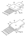
- first housing 20 A perspective view of first housing 20 is shown in the illustration of FIG. 3a and a perspective view of the second housing as a second part of sensor device 10 is shown in FIG. 1 in an unconnected state in FIG. 3b . Only the differences from the illustration in FIG. 1 will be explained below.
- a rectangular depression 440 is formed as a first formation at the edge to first side surface 45 and a second rectangular recess 445 (not shown) is formed as a second formation on the opposite edge to second side surface 50.
- a first rectangular depression 640 is formed at the edge to first side surface 245 and a second rectangular recess 645 on the opposite edge to second side surface 250.
- Rectangular depression 440 and rectangular recess 445 have dimensions substantially inverse to one another inverse, so that during joining of first housing 20 to second housing 220 a positive fit arises between the formations on the two housings 20 and 220.
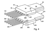
- first housing 20 and second housing 220 a perspective view of first housing 20 and second housing 220 is shown immediately before joining to sensor device 10, illustrated with the drawing documents of FIG. 1 . Only the differences relative to the illustration of the previous figures will be explained below. Rectangular elevations and depressions 440, 445, 640, and 645, arranged on the respective bottom sides 25 and 225 of first housing 20 and of second housing 220, during the joining process engage form-fittingly in one another and form a centering aid, so that the two housings 20 and 220 are positioned precisely one over the other.
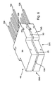
- FIG. 5 a perspective view of a second embodiment of the first housing and second housing are shown in which top side of the first housing is joined to the bottom side of the second housing. Only the differences relative to the illustration of the previous figures will be explained below.
- Rectangular elevations and depressions 740, 745, 840, and 845 arranged on the respective bottom sides 25 and 225 of first housing 20 and of second housing 220.
- rectangular depressions 940 and 945 are arranged on the respective top sides 30 and 230.
- the rectangular elevations 740 and 745 engage form-fittingly with the rectangular depressions 940 and 945 and form a centering aid, so that the two housings 20 and 220 are positioned precisely one over the other.
- Stepped formations 400 are formed in each case only on both side surfaces 45 and 50 of first housing 20 and on both side surfaces 245 and 250 of second housing 220.
- the module has larger outer dimensions on the face sides 35 of first housing 20 and on face side 235 of second housing 220 than on the two back sides 40 and 240. Because of, the first housing 20 and a second housing 220 are joined in a top side bottom side manner the five first terminal contacts 130, 132, 134, 136, and 138 of the first housing 20 and the five second terminal contacts 330, 332, 334, 336, and 338 of the second housing 220 are arranged accordantly. As an advantage both ICs are connectable crossing-free and both sensor signals 120 and 220 are in-phase.
- FIG. 6 a perspective view of a second embodiment of the first housing and second housing are shown in which the bottom side of the first housing is joined to the bottom side of the second housing. Only the differences relative to the illustration of the previous figures will be explained below.
- the rectangular elevations 740 and 745 engage form-fittingly with the rectangular depressions 840 and 845 and form a centering aid, so that the two housings 20 and 220 are positioned precisely one over the other. Because of, the first housing 20 and a second housing 220 are joined in a bottom side bottom side manner the five first terminal contacts 130, 132, 134, 136, and 138 of the first housing 20 runs counter to the five second terminal contacts 330, 332, 334, 336, and 338 of the second housing 220. As a result, both ICs are stacked such that the sensor signal 120 and 220 of both sensors comes to signal with an opposite signs to each other.
- the two housings also have an outer rectangular form and the respective terminal contacts are formed on the respective top side of the two housings.
- Other housing shapes can also be readily joined.
Landscapes
- Physics & Mathematics (AREA)
- Condensed Matter Physics & Semiconductors (AREA)
- General Physics & Mathematics (AREA)
- Measuring Magnetic Variables (AREA)
- Hall/Mr Elements (AREA)
Abstract
Description
- The invention relates to a sensor device according to the preamble of claim 1.
-
DE 10 2010 030 801 A1 discloses integrated sensors, particularly Hall sensors, which are used, inter alia, for determining rotation angles for drive shafts. Furthermore,US 5644 473 andJP 3-32050 - On this background, the object of the invention is to provide a device that refines the state of the art.
- The object is attained by a sensor device with the features of claim 1. Advantageous embodiments of the invention are the subject matter of the dependent claims.
- According to the subject matter of the invention, a sensor device is provided, having a first housing with a bottom side and a top side and a face side and a back side and a first side surface and a second side surface, whereby the face side and the back side and the two side surfaces are arranged between the top side and the bottom side and whereby in the first housing a first semiconductor body with a top surface and a back surface is provided, and a first metal substrate is formed, with a front side and a back side, and whereby a plurality of preferably metallic terminal contacts are provided for electrical contacting of a magnetic field first sensor monolithically integrated with the first semiconductor body, and whereby in each case a section of the plurality of terminal contacts penetrates the first housing on the face side, and whereby the first semiconductor body is arranged with the back surface on the front side of the first metal substrate, and the first magnetic field sensor is formed on the top surface of the first semiconductor body , and wherein the first magnetic field sensor comprises a first main extension plane, whereby said first main extension plane is arranged parallel to the top surface of the first semiconductor body, and further a second housing with a bottom side and a top side and a face side and a back side and a first side surface and a second side surface is provided, whereby the face side and the back side and the two side surfaces are arranged between the top side and the bottom side, and whereby in the second housing a second semiconductor body with a top surface and a back surface is provided, and a second metal substrate is formed, and the second semiconductor body has a front side and a back side and a plurality of metallic terminal contacts, and the metallic terminal contacts are provided for electrical contacting of a second magnetic field sensor monolithically integrated with the second semiconductor body, whereby in each case a section of the plurality of terminal contacts penetrates the second housing on the face side, and whereby the second semiconductor body is arranged with the back surface on the front side of the second metal substrate, and the second magnetic field sensor is formed on the top surface of the second semiconductor body, and wherein the second magnetic field sensor comprises a second main extension plane, whereby said second main extension plane is arranged parallel to the top surface of the second semiconductor body and whereby the two housings form a module, and to form the module the two housings are connected form-fittingly to one another in the shape of a stack by a fixing means in a way in which the bottom side of the first housing is joined preferably form-fittingly to the bottom side of the second housing or in a way in which top side of the first housing is joined to the bottom side of the second housing, and the plurality of terminal contacts of the two housings point in the same direction or the plurality of terminal contacts of the two housings penetrate the housing on the same respective outer side, and wherein the surface normal of said first main extension plane is arranged in parallel to the surface normal of said second main extension plane and wherein in a perspective view alongside to the surface normal of the first main extension first said first main extension plane overlaps with said second main extension plane, so that the divergence in flux strength of an inhomogeneous magnetic field is reduced between first magnetic field sensor and second magnetic field sensor. It should be emphasized that metal substrate is generally called as leadframe and metallic terminal contacts as parts of the leadframe are also named as pins, whereas terminal contact on the surface of the semiconductor body are called generally as pads. In other words, the terminal contact of the leadframe that is the pin penetrates the housing of the sensors.
- An advantage of the device of the invention is that the sensor device by means of joining of two individual similar or identical housings, whereby each of the two housings has a fully functional, electrically connected sensor, is provided more or less as an individual housing module. A further advantage is that the module has two sensors identical within the process variation during production. As a result, the module-like sensor device has a high failure safety. In particular, in safety-related applications and in applications in which the sensor device is not readily accessible, by means of the increased failure safety the reliability of the product can be increased substantially and the downtime costs reduced in that, for example, in case of a malfunction of one of the two sensors one can fall back on the measured values of the other sensor. A replacement of the entire sensor device can be avoided or be performed in association with a regular maintenance interval. A further advantage is that, because of the high degree of integration and the small outer dimensions of the module or the sensor device, nearly in all application cases identical ambient parameters act on both sensors; i.e., depending on the type of sensors, for example, the temperature or the strength of the magnetic field can be determined in duplicate with the sensor device at the location of the sensor device. Further, the average of the measured values of the two sensors can be determined and measurement inaccuracy can be reduced hereby.
- In a first embodiment the first main extension plane overlaps completely with the second main extension plane. In particular, the surface normal of said first main extension plane is arranged at the same point as the surface normal of the second main extension plane.
- In another embodiment, the first housing and the second housing have substantially or exactly the same the same outer dimensions. In particular, the outer dimensions of the first housing preferably do not differ from the outer dimensions of the second housing or differ at most preferably exclusively by the formations for a joining. In another preferred embodiment, catches and/or recesses are formed on the first housing and/or on the second housing in order to join the first housing with the second housing simply and cost-effectively. In another embodiment, fixing means are provided, whereby the fixing means are formed rod-shaped and each of the fixing means has a catch at a head end or at both head ends, so that one of the fixing means is formed clamp-like. It is preferred to form the fixing means separately, so that the first housing is connected force-fittingly to the second housing by means of the clamp-shaped fixing means. In another embodiment, it is preferable to provide recesses on both housings, so that in the joined state the fixing means and/or at least the catches of the fixing means are integrated into the housing and form a positive fit. It is preferred furthermore to form a planar housing exterior side after attachment of the fixing means. In an embodiment, it is preferred to form the clamp-shaped fixing means separately, i.e., not integrally with the housing. It is preferred furthermore to provide two spaced-apart fixing means along the first side and along the second side.
- In another embodiment, the one or more fixing means are in one piece to the first housing and/or to the second housing. Tests have shown that it is advantageous on the bottom side of the first housing and on the bottom side of the second housing to form a rectangular recess and a rectangular formation or notch, whereby the two formations are spaced apart. Preferably during the joining of the first housing to the second housing the rectangular notch receives the rectangular recess form-fittingly, so that after joining of the two housings to the module on the outer side of the module no fixing means project and/or no gap forms between the two housings. It is advantageous furthermore to coat the bottom side of the first housing and/or the bottom side of the second housing with a glue-like fixing means, so that after the joining a force-fitting bond forms between the two housings.
- In another embodiment, the two housings on the top side each have a stepped formation, whereby the thickness of the two housings in a first region of the step is smaller than the thickness in a second region of the step. It is preferred here that the second region abuts the face side of the particular housing.
- In another embodiment, the two housings have a stepped formation along the first side surface and/or along the second side surface, whereby the width in the first region of the step is smaller than the width in the second region of the step.
- In a preferred embodiment, the stepped formations are formed on the first housing and on the second housing in each case at the same position on the top side as on the side surface, so that the outer dimensions of the two housings, i.e., the thickness as well as the width, are smaller in the first region than in the second region.
- In another embodiment, the first housing and the second housing on the face side each have five terminal contacts, whereby in each case two terminal contacts are formed substantially shorter than the three other terminal contacts. It is preferred to form all terminal contacts in a single plane and to arrange each of the two shorter terminal contacts between two longer terminal contacts. Tests have shown that preferably signals for a so-called final test are present or are applied at the two middle terminal contacts. Such terminal contacts are generally obsolete after the final test.
- In another embodiment, the first magnetic field sensor and/or the second magnetic field sensor are made as a Hall sensor, particularly as a Hall plate. It is preferred that the Hall plate is a vertical Hall plate. In a embodiment the main extension surface of the Hall plate is orthogonal to the top surface of the semiconductor
- The invention will be described in greater detail below with reference to the drawings. In this respect, similar parts are labeled with identical designations. The illustrated embodiments are highly schematized; i.e., the distances and lateral and vertical extension are not to scale and, if not otherwise indicated, also do not have any derivable geometric relation to one another. In the drawing:
- FIG. 1
- shows a view of a first embodiment of the invention of a sensor device as a module;
- FIG. 2
- shows a perspective view of a part, not within the housing, of the sensor device of
FIG. 1 ; - FIG. 3a
- shows a perspective view of a first embodiment of a first housing as a first part of the sensor device illustrated in
FIG. 1 ; - FIG. 3b
- shows a perspective view of a first embodiment of a second housing as a second part of the sensor device illustrated in
FIG. 1 ; - FIG. 4
- shows a perspective view of the first housing and the second housing illustrated in
FIG. 3a and inFIG. 3b immediately before joining, - FIG. 5
- shows a perspective view of a second embodiment of the first housing and second housing in which top side of the first housing is joined to the bottom side of the second housing,
- FIG. 6
- shows a perspective view of a second embodiment of the first housing and second housing in which the bottom side of the first housing is joined to the bottom side of the second housing.
- The illustration in
FIG. 1 shows a view of a first embodiment of the invention of asensor device 10 formed as a module, having afirst housing 20 and asecond housing 220. It is understood that the outer dimensions offirst housing 20 are preferably substantially identical, most preferably exactly identical to the outer dimensions ofsecond housing 220. In the present case, twohousings -
First housing 20 has abottom side 25 and atop side 30. Aface side 35 and aback side 40 and afirst side surface 45 and asecond side surface 50 are arranged betweentop side 30 andbottom side 25. Further,second housing 220 has abottom side 225 and atop side 230. Aface side 235 and a back side 240 and afirst side surface 245 and asecond side surface 250 are arranged betweentop side 230 andbottom side 225. In the present case, backside 40 offirst housing 20 is connected force-fittingly to back side 240 ofsecond housing 220 to form a module. - Stepped
formations 400 are formed in each case ontop side 30 offirst housing 20 and ontop side 230 ofsecond housing 220 and on both side surfaces 45 and 50 offirst housing 20 and on both side surfaces 245 and 250 ofsecond housing 220. As a result, the module has larger outer dimensions on the face sides 35 offirst housing 20 or onface side 235 ofsecond housing 220 than on the two back sides 40 and 240. - A first sensor 120 (not shown) is integrated into
first housing 20.First housing 20 is preferably made as IC housing. A total of five firstterminal contacts first housing 20 onface side 35, whereby in each case a section of the five firstterminal contacts housing 20 and another section of the five firstterminal contacts first housing 20 and are partially molded in. The five firstterminal contacts terminal contacts - A second sensor 320 (not shown) is integrated into
second housing 220.First housing 220 is preferably made as IC housing. A total of five secondsterminal contacts first housing 220 onface side 235, whereby in each case a section of the five secondterminal contacts housing 220 and another section of the five secondterminal contacts second housing 220 and are partially molded in. The five secondterminal contacts terminal contacts terminal contacts -
First housing 20 andsecond housing 220 are connected force-fittingly to one another by a fixing means, whereby the bottom side offirst housing 20 is joined form-fittingly to the bottom side ofsecond housing 220 and is formed form-fittingly in the shape of a stack and the plurality ofterminal contacts housings - A perspective view of a part of the structure, surrounded by
first housing 20 ofsensor device 10, is shown in the illustration ofFIG. 2 . Only the differences from the illustration inFIG. 1 will be explained below. Afirst semiconductor body 100, having atop surface 105 and a back surface 110, is arranged on afirst metal substrate 115, wherebymetal substrate 115 is also called a lead frame.Metal substrate 115 has a front side 117 and a back side 119.Semiconductor body 100 is connected force-fittingly to back area 110 on front side 117. -
First sensor 120 is arranged as a monolithic part ofsemiconductor body 100 ontop surface 105, wherebyfirst sensor 120 is preferably made as a Hall sensor, most preferably as a Hall plate. A plurality of first bonding surfaces 180, so-called pads, are arranged ontop surface 105 offirst semiconductor body 100. The first bonding surfaces 180 are electrically connected byfirst bonding wires 185 to firstterminal contacts terminal contacts first semiconductor body 100 and/or tofirst metal substrate 115. In the present case, all five firstterminal contacts - In an embodiment that is not shown, it is preferred to form a first integrated circuit on
top surface 105 ofsemiconductor body 100. In this way,first sensor 120 can be supplied with an operating current and tap off a first sensor voltage and continue processing. - It should be noted that the internal structure of the part, surrounded by
second housing 220, ofsensor device 10 is identical to the structure surrounded byfirst housing 20. For example, second semiconductor body 300 is arranged on second metal substrate 315, whereby the second monolithically integrated sensor 320 is arranged on top surface 305 of second semiconductor body 300. Furthermore, second metal substrate 315 has a front side 317 and a back side 319 and second semiconductor body 300 a top surface 305 and a back surface 310. - A perspective view of
first housing 20 is shown in the illustration ofFIG. 3a and a perspective view of the second housing as a second part ofsensor device 10 is shown inFIG. 1 in an unconnected state inFIG. 3b . Only the differences from the illustration inFIG. 1 will be explained below. Onbottom side 25 offirst housing 20, arectangular depression 440 is formed as a first formation at the edge tofirst side surface 45 and a second rectangular recess 445 (not shown) is formed as a second formation on the opposite edge tosecond side surface 50. - Accordingly, on
bottom side 225 of second housing 220 a firstrectangular depression 640 is formed at the edge tofirst side surface 245 and a secondrectangular recess 645 on the opposite edge tosecond side surface 250. -
Rectangular depression 440 andrectangular recess 445 have dimensions substantially inverse to one another inverse, so that during joining offirst housing 20 to second housing 220 a positive fit arises between the formations on the twohousings - In the illustration of
FIG. 4 , a perspective view offirst housing 20 andsecond housing 220 is shown immediately before joining tosensor device 10, illustrated with the drawing documents ofFIG. 1 . Only the differences relative to the illustration of the previous figures will be explained below. Rectangular elevations anddepressions first housing 20 and ofsecond housing 220, during the joining process engage form-fittingly in one another and form a centering aid, so that the twohousings - In the illustration of
FIG. 5 , a perspective view of a second embodiment of the first housing and second housing are shown in which top side of the first housing is joined to the bottom side of the second housing. Only the differences relative to the illustration of the previous figures will be explained below. Rectangular elevations anddepressions first housing 20 and ofsecond housing 220. On the respectivetop sides rectangular depressions 940 and 945 are arranged. During the joining process therectangular elevations rectangular depressions 940 and 945 and form a centering aid, so that the twohousings formations 400 are formed in each case only on both side surfaces 45 and 50 offirst housing 20 and on both side surfaces 245 and 250 ofsecond housing 220. As a result, the module has larger outer dimensions on the face sides 35 offirst housing 20 and onface side 235 ofsecond housing 220 than on the two back sides 40 and 240. Because of, thefirst housing 20 and asecond housing 220 are joined in a top side bottom side manner the five firstterminal contacts first housing 20 and the five secondterminal contacts second housing 220 are arranged accordantly. As an advantage both ICs are connectable crossing-free and both sensor signals 120 and 220 are in-phase. - In the illustration of
FIG. 6 , a perspective view of a second embodiment of the first housing and second housing are shown in which the bottom side of the first housing is joined to the bottom side of the second housing. Only the differences relative to the illustration of the previous figures will be explained below. - During the joining process the
rectangular elevations rectangular depressions housings first housing 20 and asecond housing 220 are joined in a bottom side bottom side manner the five firstterminal contacts first housing 20 runs counter to the five secondterminal contacts second housing 220. As a result, both ICs are stacked such that thesensor signal - It should be noted that in an embodiment that is not shown, the two housings also have an outer rectangular form and the respective terminal contacts are formed on the respective top side of the two housings. Other housing shapes can also be readily joined.
-
-
Sensor device 10 -
first housing 20 with
bottom side 25
top side 30
face side 35
backside 40
first side surface 45
second side surface 50 -
first semiconductor body 100top surface 105
back surface 110 -
first metal substrate 115
a front side 117
a back side 119 -
first sensor 120 - first
terminal contacts - first bonding surfaces 180
-
first bonding wires 185 -
second housing 220
bottom side 225
top side 230
face side 235
back side 240
first side surface 245
second side surface 250 - second metal substrate 315
front side 317
back side 319 - second semiconductor body 300
top surface 305
back surface 310 - second sensor 320
- second
terminal contacts - stepped
formations 400 - first
rectangular depression 440 - second
rectangular recess 445 - first
rectangular depression 640 - second
rectangular recess 645 -
rectangular elevations -
rectangular depressions -
rectangular depressions 940, 945
Claims (16)
- A sensor device (10), having
a first housing (20) with a bottom side (25) and a top side (30) and a face side (35) and a back side (40) and a first side surface (45) and a second side surface (50), whereby the face side (35) and the back side (40) and the two side surfaces (45, 50) are arranged between the top side (30) and the bottom side (25), and
a first semiconductor body (100) with a top surface (105) and a back surface (110) is formed in the first housing (20), and
a first metal substrate (115), with a front side (117) and a back side (119), and
a plurality of terminal contacts (130, 132, 134, 136, 138), arranged on the top surface (105) of the semiconductor body (100), for electrical contacting of a first magnetic field sensor (120), monolithically integrated with the first semiconductor body (100), whereby in each case a section of the plurality of terminal contacts 132, 134, 136, 138) penetrates the first housing (20) on the face side (35), and the first semiconductor body (100) is arranged with the back surface (110) on the front side (117) of the first metal substrate (115), and the first magnetic field sensor (120) is formed on the top surface (105) of the first semiconductor body (100), and wherein the first magnetic field sensor comprises a first main extension plane, whereby said first main extension plane is arranged parallel to the top surface (105) of the first semiconductor body (100), and
a second housing (220) with a bottom side (225) and a top side (230) and a face side (235) and a back side (240) and a first side surface (245) and a second side surface (250), whereby the face side (235) and the back side (240) and the two side surfaces (245, 250) are arranged between the top side (230) and the bottom side (235), and
in the second housing (220) a second semiconductor body (300) with a top surface (305) and a back surface (310) are formed, and
a second metal substrate (315), with a front side (317) and a back side (319) and a plurality of second terminal contacts (330, 332, 334, 336, 338) for electrical contacting of a second magnetic field sensor (320), monolithically integrated with
the second semiconductor body (300), whereby in each case a section of the plurality of second terminal contacts (330, 332, 334, 336, 338) penetrates the second housing (220) on the face side (335), and the second semiconductor body (300) is arranged with the back surface (310) on the front side (317) of the second metal substrate (315), and the second magnetic field sensor (320) is formed on the top surface (305) of the second semiconductor body (300), and wherein the second magnetic field sensor comprises a second main extension plane, whereby said second main extension plane is arranged parallel to the top surface (305) of the second semiconductor body (300),
characterized in that
the two housings (20, 220) form a module, whereby the two housings (20, 220) are connected form-fittingly to one another in the shape of a stack by a fixing means- in a way in which the bottom side (25) of the first housing (20) is joined to the bottom side (225) of the second housing (220),- or in a way in which top side (30) of the first housing (20) is joined to the bottom side (225) of the second housing (220),and the plurality of terminal contacts (130, 132, 134, 136, 138, 330, 332, 334, 336, 338) of the two housings (20, 220) point in the same direction or the plurality of terminal contacts (130, 132, 134, 136, 138, 330, 332, 334, 336, 338) of the two housings (20, 220) penetrates the respective housing on the respective same outer side, and wherein the surface normal of said first main extension plane is arranged in parallel to the surface normal of said second main extension plane and wherein in a perspective view alongside to the surface normal of the first main extension first said first main extension plane overlaps with said second main extension plane, so that the divergence in flux strength of an inhomogeneous magnetic field is reduced between first magnetic field sensor and second magnetic field sensor. - The sensor device (10) according to claim 1, characterized in that the first main extension plane overlaps completely with the second main extension plane.
- The sensor device (10) according to claim 1, characterized in that the surface normal of said first main extension plane is arranged at the same point as the surface normal of the second main extension plane.
- The sensor device (10) according to one of the preceding claims, characterized in that the first housing (20) and the second housing (220) have substantially the same or exactly the same outer dimensions.
- The sensor device (10) according to one of the preceding claims characterized in that catches and/or recesses are formed on the first housing (20) and/or on the second housing (220).
- The sensor device (10) according to one of the preceding claims, characterized in that the fixing means are formed rod-shaped and each fixing means has a catch at both head ends.
- The sensor device (10) according to one of the preceding claims, characterized in that two spaced-apart fixing means are provided along the first side surface (45, 245) and along the second side surface (50, 250).
- The sensor device (10) according to one of the preceding claims, characterized in that the catches form a positive fit with the recesses.
- The sensor device (10) according to one of the preceding claims, characterized in that the fixing means are in one piece to the housing (20, 220) on the first housing (20) and/or on the second housing (220) and comprise rectangular elevations (440, 640) and/or rectangular depressions (445, 465).
- The sensor device (10) according to one of the preceding claims, characterized in that the two housings (20, 220) on the top side each have a stepped formation (400) and the thickness in a first region of the step is smaller than the thickness in a second region of the step.
- The sensor device (10) according to claim 10, characterized in that the second region abuts the face side of the two housings (20, 220).
- The sensor device (10) according to one of the preceding claims, characterized in that the two housings (20, 220) have a stepped formation (400) along the first side surfaces (45, 245) and/or along the second side surfaces (50, 250) and the width in the first region of the step is smaller than the width in the second region of the step and abuts the second region on the face side (35, 235) of the two housings (20; 220).
- The sensor device (10) according to one of the preceding claims, characterized in that on the first housing (20) and on the second housing (220) the stepped formation (400) is formed at the same position on the respective top side (30, 230) as on the respective side surface (45, 50, 245, 250), so that the outer dimensions of the two housings (20, 220) are smaller in the first region than in the second region.
- The sensor device (10) according to one of the preceding claims, characterized in that the first magnetic field sensor (20) and/or the second magnetic field sensor (220) are Hall sensors.
- The sensor device (10) according to claim 15, characterized in that the Hall sensor is formed as a vertical Hall plate.
- The sensor device (10) according to claim 16, characterized in that the main extension surface of the Hall plate is orthogonal to the top surface of the semiconductor.
Priority Applications (3)
| Application Number | Priority Date | Filing Date | Title |
|---|---|---|---|
| EP14000112.4A EP2894489B1 (en) | 2014-01-13 | 2014-01-13 | Sensor device |
| JP2014231442A JP6218721B2 (en) | 2014-01-13 | 2014-11-14 | Sensor device |
| US14/595,902 US9632148B2 (en) | 2014-01-13 | 2015-01-13 | Sensor device |
Applications Claiming Priority (1)
| Application Number | Priority Date | Filing Date | Title |
|---|---|---|---|
| EP14000112.4A EP2894489B1 (en) | 2014-01-13 | 2014-01-13 | Sensor device |
Publications (2)
| Publication Number | Publication Date |
|---|---|
| EP2894489A1 true EP2894489A1 (en) | 2015-07-15 |
| EP2894489B1 EP2894489B1 (en) | 2019-03-13 |
Family
ID=49958228
Family Applications (1)
| Application Number | Title | Priority Date | Filing Date |
|---|---|---|---|
| EP14000112.4A Active EP2894489B1 (en) | 2014-01-13 | 2014-01-13 | Sensor device |
Country Status (3)
| Country | Link |
|---|---|
| US (1) | US9632148B2 (en) |
| EP (1) | EP2894489B1 (en) |
| JP (1) | JP6218721B2 (en) |
Cited By (1)
| Publication number | Priority date | Publication date | Assignee | Title |
|---|---|---|---|---|
| EP4163987A4 (en) * | 2020-06-03 | 2024-07-10 | TDK Corporation | MAGNETIC FIELD DETECTOR AND ARRAY OF MAGNETIC FIELD DETECTORS |
Families Citing this family (7)
| Publication number | Priority date | Publication date | Assignee | Title |
|---|---|---|---|---|
| JP2017075790A (en) * | 2015-10-13 | 2017-04-20 | 株式会社東海理化電機製作所 | Magnetic sensor device |
| JP6677080B2 (en) | 2016-05-30 | 2020-04-08 | 株式会社デンソー | Method for manufacturing semiconductor device |
| US10759276B2 (en) | 2016-07-12 | 2020-09-01 | Panasonic Intellectual Property Management Co., Ltd. | Magnetic sensor and detection device using same |
| JP7035602B2 (en) * | 2018-02-16 | 2022-03-15 | Tdk株式会社 | Magnetic sensor and magnetic sensor connector equipped with it |
| KR102554225B1 (en) * | 2021-05-17 | 2023-07-12 | 재단법인대구경북과학기술원 | 3D magnetic field measurement device and the magnetic field mapping system |
| TWI858427B (en) * | 2021-11-02 | 2024-10-11 | 實盈光電股份有限公司 | Test electronical connector device and manufacturing method of terminal base thereof |
| TWI789095B (en) | 2021-11-02 | 2023-01-01 | 實盈光電股份有限公司 | Test electronical connector device and manufacturing method of terminal base thereof |
Citations (13)
| Publication number | Priority date | Publication date | Assignee | Title |
|---|---|---|---|---|
| JPH0332050A (en) | 1989-06-28 | 1991-02-12 | Mitsubishi Electric Corp | Ic package |
| JPH05291482A (en) * | 1992-04-08 | 1993-11-05 | Mitsubishi Electric Corp | Hybrid integrated circuit device and fabrication thereof |
| US5644473A (en) | 1995-08-21 | 1997-07-01 | Mitsubishi Semiconductor America, Inc. | Carriers for IC packages |
| EP1160887A2 (en) * | 2000-05-15 | 2001-12-05 | Mannesmann VDO Aktiengesellschaft | Hall-effect sensor element with integrated condensers |
| EP1271159A2 (en) * | 2001-06-15 | 2003-01-02 | Sanken Electric Co., Ltd. | Hall-effect current detector |
| US20040080308A1 (en) * | 2002-10-28 | 2004-04-29 | Hirokazu Goto | Electric current detector with hall effect sensor |
| US20070279053A1 (en) * | 2006-05-12 | 2007-12-06 | Taylor William P | Integrated current sensor |
| US20080237818A1 (en) * | 2007-03-29 | 2008-10-02 | Engel Raymond W | Methods and apparatus for multi-stage molding of integrated circuit package |
| US20090294882A1 (en) * | 2008-05-30 | 2009-12-03 | Infineon Technologies North America Corp. | Methods and systems for magnetic sensing |
| US20110133732A1 (en) * | 2009-12-03 | 2011-06-09 | Allegro Microsystems, Inc. | Methods and apparatus for enhanced frequency response of magnetic sensors |
| DE102010030801A1 (en) | 2010-07-01 | 2012-01-05 | Vs Sensorik Gmbh | Rotary transducer e.g. multi-turn rotary transducer, for determination of absolute rotational position of rotatable shaft, has signal transmitter and signal receiver for detecting position of gear element |
| US20120086090A1 (en) * | 2006-07-14 | 2012-04-12 | Allegro Microsystems, Inc. | Methods and apparatus for passive attachment of components for integrated circuits |
| US20120146164A1 (en) * | 2010-12-09 | 2012-06-14 | Udo Ausserlechner | Magnetic field current sensors |
Family Cites Families (11)
| Publication number | Priority date | Publication date | Assignee | Title |
|---|---|---|---|---|
| JPH0685165A (en) * | 1992-09-01 | 1994-03-25 | Seiko Epson Corp | Semiconductor device and manufacture thereof |
| KR0149798B1 (en) * | 1994-04-15 | 1998-10-01 | 모리시다 요이치 | Semiconductor device and method of manufacture and lead frame |
| JP4055609B2 (en) * | 2003-03-03 | 2008-03-05 | 株式会社デンソー | Magnetic sensor manufacturing method |
| DE102005060713B4 (en) * | 2005-12-19 | 2019-01-24 | Austriamicrosystems Ag | Magnetic field sensor arrangement and method for non-contact measurement of a magnetic field |
| JP4863953B2 (en) * | 2007-08-30 | 2012-01-25 | 日立オートモティブシステムズ株式会社 | Physical quantity conversion sensor and motor control system using the same |
| JP5593704B2 (en) * | 2010-01-14 | 2014-09-24 | 株式会社デンソー | Magnetic detection element, rotation angle detection device and stroke amount detection device using the same |
| US9494660B2 (en) * | 2012-03-20 | 2016-11-15 | Allegro Microsystems, Llc | Integrated circuit package having a split lead frame |
| US8907669B2 (en) * | 2012-07-24 | 2014-12-09 | Allegro Microsystems, Llc | Circuits and techniques for adjusting a sensitivity of a closed-loop current sensor |
| US9305876B2 (en) * | 2013-02-01 | 2016-04-05 | Infineon Technologies Austria Ag | Device including a semiconductor chip and wires |
| CH707687B1 (en) * | 2013-03-08 | 2016-09-15 | Melexis Technologies Nv | Current sensor. |
| US9658296B2 (en) * | 2013-07-10 | 2017-05-23 | Infineon Technologies Ag | Current sensor device |
-
2014
- 2014-01-13 EP EP14000112.4A patent/EP2894489B1/en active Active
- 2014-11-14 JP JP2014231442A patent/JP6218721B2/en active Active
-
2015
- 2015-01-13 US US14/595,902 patent/US9632148B2/en active Active
Patent Citations (13)
| Publication number | Priority date | Publication date | Assignee | Title |
|---|---|---|---|---|
| JPH0332050A (en) | 1989-06-28 | 1991-02-12 | Mitsubishi Electric Corp | Ic package |
| JPH05291482A (en) * | 1992-04-08 | 1993-11-05 | Mitsubishi Electric Corp | Hybrid integrated circuit device and fabrication thereof |
| US5644473A (en) | 1995-08-21 | 1997-07-01 | Mitsubishi Semiconductor America, Inc. | Carriers for IC packages |
| EP1160887A2 (en) * | 2000-05-15 | 2001-12-05 | Mannesmann VDO Aktiengesellschaft | Hall-effect sensor element with integrated condensers |
| EP1271159A2 (en) * | 2001-06-15 | 2003-01-02 | Sanken Electric Co., Ltd. | Hall-effect current detector |
| US20040080308A1 (en) * | 2002-10-28 | 2004-04-29 | Hirokazu Goto | Electric current detector with hall effect sensor |
| US20070279053A1 (en) * | 2006-05-12 | 2007-12-06 | Taylor William P | Integrated current sensor |
| US20120086090A1 (en) * | 2006-07-14 | 2012-04-12 | Allegro Microsystems, Inc. | Methods and apparatus for passive attachment of components for integrated circuits |
| US20080237818A1 (en) * | 2007-03-29 | 2008-10-02 | Engel Raymond W | Methods and apparatus for multi-stage molding of integrated circuit package |
| US20090294882A1 (en) * | 2008-05-30 | 2009-12-03 | Infineon Technologies North America Corp. | Methods and systems for magnetic sensing |
| US20110133732A1 (en) * | 2009-12-03 | 2011-06-09 | Allegro Microsystems, Inc. | Methods and apparatus for enhanced frequency response of magnetic sensors |
| DE102010030801A1 (en) | 2010-07-01 | 2012-01-05 | Vs Sensorik Gmbh | Rotary transducer e.g. multi-turn rotary transducer, for determination of absolute rotational position of rotatable shaft, has signal transmitter and signal receiver for detecting position of gear element |
| US20120146164A1 (en) * | 2010-12-09 | 2012-06-14 | Udo Ausserlechner | Magnetic field current sensors |
Cited By (1)
| Publication number | Priority date | Publication date | Assignee | Title |
|---|---|---|---|---|
| EP4163987A4 (en) * | 2020-06-03 | 2024-07-10 | TDK Corporation | MAGNETIC FIELD DETECTOR AND ARRAY OF MAGNETIC FIELD DETECTORS |
Also Published As
| Publication number | Publication date |
|---|---|
| US20150198678A1 (en) | 2015-07-16 |
| US9632148B2 (en) | 2017-04-25 |
| EP2894489B1 (en) | 2019-03-13 |
| JP6218721B2 (en) | 2017-10-25 |
| JP2015132595A (en) | 2015-07-23 |
Similar Documents
| Publication | Publication Date | Title |
|---|---|---|
| EP2894489B1 (en) | Sensor device | |
| CN104126107B (en) | Physical quantity sensor and manufacturing method of physical quantity sensor | |
| CN103649762B (en) | Current sensor substrate and current sensor | |
| JP5165963B2 (en) | Magnetic sensor and manufacturing method thereof | |
| EP3067664B1 (en) | Rotational angle detecting sensor | |
| CN104395722B (en) | pressure detection device | |
| US10629887B2 (en) | Secondary battery | |
| US8094463B2 (en) | Crystal oscillator for surface mounting | |
| US20080083287A1 (en) | Load Sensor And Manufacturing Method Of The Same | |
| JP2017050489A (en) | Semiconductor package and manufacturing method of the same | |
| JP2014048072A (en) | Pressure sensor module | |
| US10586773B2 (en) | Semiconductor device | |
| US10304777B2 (en) | Semiconductor device having a plurality of semiconductor modules connected by a connection component | |
| US10251295B2 (en) | Electronic device and method of producing the same | |
| US9865585B2 (en) | LED module and method of manufacturing the same | |
| US10854540B2 (en) | Packaged IC component | |
| US20170234907A1 (en) | Inspection terminal unit, probe card, and method for manufacturing inspection terminal unit | |
| CN110168388B (en) | Electronic device and connector | |
| JP5262771B2 (en) | Manufacturing method of magnetic sensor and magnetic sensor | |
| US12510587B2 (en) | Semiconductor device and inspection method for semiconductor device | |
| US20150123291A1 (en) | Method for manufacturing a flip-chip circuit configuration and the flip-chip circuit configuration | |
| US6008639A (en) | Magnetic sensor having a main electrical circuit base with a crack forming area | |
| US9780470B2 (en) | Contact device system | |
| TWI457572B (en) | Method for testing electric products | |
| KR200304113Y1 (en) | Probe card for testing semiconductor |
Legal Events
| Date | Code | Title | Description |
|---|---|---|---|
| PUAI | Public reference made under article 153(3) epc to a published international application that has entered the european phase |
Free format text: ORIGINAL CODE: 0009012 |
|
| 17P | Request for examination filed |
Effective date: 20140113 |
|
| AK | Designated contracting states |
Kind code of ref document: A1 Designated state(s): AL AT BE BG CH CY CZ DE DK EE ES FI FR GB GR HR HU IE IS IT LI LT LU LV MC MK MT NL NO PL PT RO RS SE SI SK SM TR |
|
| AX | Request for extension of the european patent |
Extension state: BA ME |
|
| R17P | Request for examination filed (corrected) |
Effective date: 20150806 |
|
| RBV | Designated contracting states (corrected) |
Designated state(s): AL AT BE BG CH CY CZ DE DK EE ES FI FR GB GR HR HU IE IS IT LI LT LU LV MC MK MT NL NO PL PT RO RS SE SI SK SM TR |
|
| RAP1 | Party data changed (applicant data changed or rights of an application transferred) |
Owner name: TDK-MICRONAS GMBH |
|
| GRAP | Despatch of communication of intention to grant a patent |
Free format text: ORIGINAL CODE: EPIDOSNIGR1 |
|
| STAA | Information on the status of an ep patent application or granted ep patent |
Free format text: STATUS: GRANT OF PATENT IS INTENDED |
|
| RIC1 | Information provided on ipc code assigned before grant |
Ipc: G01R 33/09 20060101ALI20181024BHEP Ipc: G01R 33/00 20060101AFI20181024BHEP Ipc: G01R 33/07 20060101ALI20181024BHEP |
|
| INTG | Intention to grant announced |
Effective date: 20181122 |
|
| GRAS | Grant fee paid |
Free format text: ORIGINAL CODE: EPIDOSNIGR3 |
|
| GRAA | (expected) grant |
Free format text: ORIGINAL CODE: 0009210 |
|
| STAA | Information on the status of an ep patent application or granted ep patent |
Free format text: STATUS: THE PATENT HAS BEEN GRANTED |
|
| AK | Designated contracting states |
Kind code of ref document: B1 Designated state(s): AL AT BE BG CH CY CZ DE DK EE ES FI FR GB GR HR HU IE IS IT LI LT LU LV MC MK MT NL NO PL PT RO RS SE SI SK SM TR |
|
| REG | Reference to a national code |
Ref country code: GB Ref legal event code: FG4D |
|
| REG | Reference to a national code |
Ref country code: AT Ref legal event code: REF Ref document number: 1108435 Country of ref document: AT Kind code of ref document: T Effective date: 20190315 Ref country code: CH Ref legal event code: EP |
|
| REG | Reference to a national code |
Ref country code: IE Ref legal event code: FG4D |
|
| REG | Reference to a national code |
Ref country code: DE Ref legal event code: R096 Ref document number: 602014042653 Country of ref document: DE |
|
| REG | Reference to a national code |
Ref country code: NL Ref legal event code: MP Effective date: 20190313 |
|
| REG | Reference to a national code |
Ref country code: LT Ref legal event code: MG4D |
|
| PG25 | Lapsed in a contracting state [announced via postgrant information from national office to epo] |
Ref country code: LT Free format text: LAPSE BECAUSE OF FAILURE TO SUBMIT A TRANSLATION OF THE DESCRIPTION OR TO PAY THE FEE WITHIN THE PRESCRIBED TIME-LIMIT Effective date: 20190313 Ref country code: SE Free format text: LAPSE BECAUSE OF FAILURE TO SUBMIT A TRANSLATION OF THE DESCRIPTION OR TO PAY THE FEE WITHIN THE PRESCRIBED TIME-LIMIT Effective date: 20190313 Ref country code: FI Free format text: LAPSE BECAUSE OF FAILURE TO SUBMIT A TRANSLATION OF THE DESCRIPTION OR TO PAY THE FEE WITHIN THE PRESCRIBED TIME-LIMIT Effective date: 20190313 Ref country code: NO Free format text: LAPSE BECAUSE OF FAILURE TO SUBMIT A TRANSLATION OF THE DESCRIPTION OR TO PAY THE FEE WITHIN THE PRESCRIBED TIME-LIMIT Effective date: 20190613 |
|
| PG25 | Lapsed in a contracting state [announced via postgrant information from national office to epo] |
Ref country code: BG Free format text: LAPSE BECAUSE OF FAILURE TO SUBMIT A TRANSLATION OF THE DESCRIPTION OR TO PAY THE FEE WITHIN THE PRESCRIBED TIME-LIMIT Effective date: 20190613 Ref country code: GR Free format text: LAPSE BECAUSE OF FAILURE TO SUBMIT A TRANSLATION OF THE DESCRIPTION OR TO PAY THE FEE WITHIN THE PRESCRIBED TIME-LIMIT Effective date: 20190614 Ref country code: HR Free format text: LAPSE BECAUSE OF FAILURE TO SUBMIT A TRANSLATION OF THE DESCRIPTION OR TO PAY THE FEE WITHIN THE PRESCRIBED TIME-LIMIT Effective date: 20190313 Ref country code: LV Free format text: LAPSE BECAUSE OF FAILURE TO SUBMIT A TRANSLATION OF THE DESCRIPTION OR TO PAY THE FEE WITHIN THE PRESCRIBED TIME-LIMIT Effective date: 20190313 Ref country code: RS Free format text: LAPSE BECAUSE OF FAILURE TO SUBMIT A TRANSLATION OF THE DESCRIPTION OR TO PAY THE FEE WITHIN THE PRESCRIBED TIME-LIMIT Effective date: 20190313 Ref country code: NL Free format text: LAPSE BECAUSE OF FAILURE TO SUBMIT A TRANSLATION OF THE DESCRIPTION OR TO PAY THE FEE WITHIN THE PRESCRIBED TIME-LIMIT Effective date: 20190313 |
|
| REG | Reference to a national code |
Ref country code: AT Ref legal event code: MK05 Ref document number: 1108435 Country of ref document: AT Kind code of ref document: T Effective date: 20190313 |
|
| PG25 | Lapsed in a contracting state [announced via postgrant information from national office to epo] |
Ref country code: AL Free format text: LAPSE BECAUSE OF FAILURE TO SUBMIT A TRANSLATION OF THE DESCRIPTION OR TO PAY THE FEE WITHIN THE PRESCRIBED TIME-LIMIT Effective date: 20190313 Ref country code: SK Free format text: LAPSE BECAUSE OF FAILURE TO SUBMIT A TRANSLATION OF THE DESCRIPTION OR TO PAY THE FEE WITHIN THE PRESCRIBED TIME-LIMIT Effective date: 20190313 Ref country code: PT Free format text: LAPSE BECAUSE OF FAILURE TO SUBMIT A TRANSLATION OF THE DESCRIPTION OR TO PAY THE FEE WITHIN THE PRESCRIBED TIME-LIMIT Effective date: 20190713 Ref country code: IT Free format text: LAPSE BECAUSE OF FAILURE TO SUBMIT A TRANSLATION OF THE DESCRIPTION OR TO PAY THE FEE WITHIN THE PRESCRIBED TIME-LIMIT Effective date: 20190313 Ref country code: CZ Free format text: LAPSE BECAUSE OF FAILURE TO SUBMIT A TRANSLATION OF THE DESCRIPTION OR TO PAY THE FEE WITHIN THE PRESCRIBED TIME-LIMIT Effective date: 20190313 Ref country code: RO Free format text: LAPSE BECAUSE OF FAILURE TO SUBMIT A TRANSLATION OF THE DESCRIPTION OR TO PAY THE FEE WITHIN THE PRESCRIBED TIME-LIMIT Effective date: 20190313 Ref country code: ES Free format text: LAPSE BECAUSE OF FAILURE TO SUBMIT A TRANSLATION OF THE DESCRIPTION OR TO PAY THE FEE WITHIN THE PRESCRIBED TIME-LIMIT Effective date: 20190313 Ref country code: EE Free format text: LAPSE BECAUSE OF FAILURE TO SUBMIT A TRANSLATION OF THE DESCRIPTION OR TO PAY THE FEE WITHIN THE PRESCRIBED TIME-LIMIT Effective date: 20190313 |
|
| PG25 | Lapsed in a contracting state [announced via postgrant information from national office to epo] |
Ref country code: SM Free format text: LAPSE BECAUSE OF FAILURE TO SUBMIT A TRANSLATION OF THE DESCRIPTION OR TO PAY THE FEE WITHIN THE PRESCRIBED TIME-LIMIT Effective date: 20190313 Ref country code: PL Free format text: LAPSE BECAUSE OF FAILURE TO SUBMIT A TRANSLATION OF THE DESCRIPTION OR TO PAY THE FEE WITHIN THE PRESCRIBED TIME-LIMIT Effective date: 20190313 |
|
| REG | Reference to a national code |
Ref country code: DE Ref legal event code: R097 Ref document number: 602014042653 Country of ref document: DE |
|
| PG25 | Lapsed in a contracting state [announced via postgrant information from national office to epo] |
Ref country code: IS Free format text: LAPSE BECAUSE OF FAILURE TO SUBMIT A TRANSLATION OF THE DESCRIPTION OR TO PAY THE FEE WITHIN THE PRESCRIBED TIME-LIMIT Effective date: 20190713 Ref country code: AT Free format text: LAPSE BECAUSE OF FAILURE TO SUBMIT A TRANSLATION OF THE DESCRIPTION OR TO PAY THE FEE WITHIN THE PRESCRIBED TIME-LIMIT Effective date: 20190313 |
|
| PLBE | No opposition filed within time limit |
Free format text: ORIGINAL CODE: 0009261 |
|
| STAA | Information on the status of an ep patent application or granted ep patent |
Free format text: STATUS: NO OPPOSITION FILED WITHIN TIME LIMIT |
|
| PG25 | Lapsed in a contracting state [announced via postgrant information from national office to epo] |
Ref country code: DK Free format text: LAPSE BECAUSE OF FAILURE TO SUBMIT A TRANSLATION OF THE DESCRIPTION OR TO PAY THE FEE WITHIN THE PRESCRIBED TIME-LIMIT Effective date: 20190313 |
|
| 26N | No opposition filed |
Effective date: 20191216 |
|
| PG25 | Lapsed in a contracting state [announced via postgrant information from national office to epo] |
Ref country code: SI Free format text: LAPSE BECAUSE OF FAILURE TO SUBMIT A TRANSLATION OF THE DESCRIPTION OR TO PAY THE FEE WITHIN THE PRESCRIBED TIME-LIMIT Effective date: 20190313 |
|
| PG25 | Lapsed in a contracting state [announced via postgrant information from national office to epo] |
Ref country code: TR Free format text: LAPSE BECAUSE OF FAILURE TO SUBMIT A TRANSLATION OF THE DESCRIPTION OR TO PAY THE FEE WITHIN THE PRESCRIBED TIME-LIMIT Effective date: 20190313 |
|
| PGFP | Annual fee paid to national office [announced via postgrant information from national office to epo] |
Ref country code: GB Payment date: 20200124 Year of fee payment: 7 |
|
| PGFP | Annual fee paid to national office [announced via postgrant information from national office to epo] |
Ref country code: FR Payment date: 20200121 Year of fee payment: 7 |
|
| PG25 | Lapsed in a contracting state [announced via postgrant information from national office to epo] |
Ref country code: MC Free format text: LAPSE BECAUSE OF FAILURE TO SUBMIT A TRANSLATION OF THE DESCRIPTION OR TO PAY THE FEE WITHIN THE PRESCRIBED TIME-LIMIT Effective date: 20190313 |
|
| REG | Reference to a national code |
Ref country code: CH Ref legal event code: PL |
|
| REG | Reference to a national code |
Ref country code: BE Ref legal event code: MM Effective date: 20200131 |
|
| PG25 | Lapsed in a contracting state [announced via postgrant information from national office to epo] |
Ref country code: LU Free format text: LAPSE BECAUSE OF NON-PAYMENT OF DUE FEES Effective date: 20200113 |
|
| PG25 | Lapsed in a contracting state [announced via postgrant information from national office to epo] |
Ref country code: CH Free format text: LAPSE BECAUSE OF NON-PAYMENT OF DUE FEES Effective date: 20200131 Ref country code: BE Free format text: LAPSE BECAUSE OF NON-PAYMENT OF DUE FEES Effective date: 20200131 Ref country code: LI Free format text: LAPSE BECAUSE OF NON-PAYMENT OF DUE FEES Effective date: 20200131 |
|
| PG25 | Lapsed in a contracting state [announced via postgrant information from national office to epo] |
Ref country code: IE Free format text: LAPSE BECAUSE OF NON-PAYMENT OF DUE FEES Effective date: 20200113 |
|
| GBPC | Gb: european patent ceased through non-payment of renewal fee |
Effective date: 20210113 |
|
| PG25 | Lapsed in a contracting state [announced via postgrant information from national office to epo] |
Ref country code: FR Free format text: LAPSE BECAUSE OF NON-PAYMENT OF DUE FEES Effective date: 20210131 |
|
| PG25 | Lapsed in a contracting state [announced via postgrant information from national office to epo] |
Ref country code: GB Free format text: LAPSE BECAUSE OF NON-PAYMENT OF DUE FEES Effective date: 20210113 |
|
| PG25 | Lapsed in a contracting state [announced via postgrant information from national office to epo] |
Ref country code: MT Free format text: LAPSE BECAUSE OF FAILURE TO SUBMIT A TRANSLATION OF THE DESCRIPTION OR TO PAY THE FEE WITHIN THE PRESCRIBED TIME-LIMIT Effective date: 20190313 Ref country code: CY Free format text: LAPSE BECAUSE OF FAILURE TO SUBMIT A TRANSLATION OF THE DESCRIPTION OR TO PAY THE FEE WITHIN THE PRESCRIBED TIME-LIMIT Effective date: 20190313 |
|
| PG25 | Lapsed in a contracting state [announced via postgrant information from national office to epo] |
Ref country code: MK Free format text: LAPSE BECAUSE OF FAILURE TO SUBMIT A TRANSLATION OF THE DESCRIPTION OR TO PAY THE FEE WITHIN THE PRESCRIBED TIME-LIMIT Effective date: 20190313 |
|
| PGFP | Annual fee paid to national office [announced via postgrant information from national office to epo] |
Ref country code: DE Payment date: 20260121 Year of fee payment: 13 |