EP2890015A1 - Analog-to-digital converting device - Google Patents
Analog-to-digital converting device Download PDFInfo
- Publication number
- EP2890015A1 EP2890015A1 EP14197322.2A EP14197322A EP2890015A1 EP 2890015 A1 EP2890015 A1 EP 2890015A1 EP 14197322 A EP14197322 A EP 14197322A EP 2890015 A1 EP2890015 A1 EP 2890015A1
- Authority
- EP
- European Patent Office
- Prior art keywords
- signal
- analog
- digital
- generate
- filter
- Prior art date
- Legal status (The legal status is an assumption and is not a legal conclusion. Google has not performed a legal analysis and makes no representation as to the accuracy of the status listed.)
- Ceased
Links
- 238000001914 filtration Methods 0.000 claims description 38
- 239000003990 capacitor Substances 0.000 claims description 36
- 230000003111 delayed effect Effects 0.000 claims description 33
- 238000000034 method Methods 0.000 description 6
- 238000010586 diagram Methods 0.000 description 4
- 230000000694 effects Effects 0.000 description 3
- 238000012546 transfer Methods 0.000 description 3
- 238000004891 communication Methods 0.000 description 2
- 238000013461 design Methods 0.000 description 2
- 229920005994 diacetyl cellulose Polymers 0.000 description 2
- 230000001419 dependent effect Effects 0.000 description 1
- 238000011161 development Methods 0.000 description 1
- 230000018109 developmental process Effects 0.000 description 1
- 239000004065 semiconductor Substances 0.000 description 1
- 238000007493 shaping process Methods 0.000 description 1
Images





Classifications
-
- H—ELECTRICITY
- H03—ELECTRONIC CIRCUITRY
- H03M—CODING; DECODING; CODE CONVERSION IN GENERAL
- H03M1/00—Analogue/digital conversion; Digital/analogue conversion
- H03M1/001—Analogue/digital/analogue conversion
-
- H—ELECTRICITY
- H03—ELECTRONIC CIRCUITRY
- H03M—CODING; DECODING; CODE CONVERSION IN GENERAL
- H03M3/00—Conversion of analogue values to or from differential modulation
- H03M3/30—Delta-sigma modulation
- H03M3/322—Continuously compensating for, or preventing, undesired influence of physical parameters
- H03M3/324—Continuously compensating for, or preventing, undesired influence of physical parameters characterised by means or methods for compensating or preventing more than one type of error at a time, e.g. by synchronisation or using a ratiometric arrangement
- H03M3/344—Continuously compensating for, or preventing, undesired influence of physical parameters characterised by means or methods for compensating or preventing more than one type of error at a time, e.g. by synchronisation or using a ratiometric arrangement by filtering other than the noise-shaping inherent to delta-sigma modulators, e.g. anti-aliasing
-
- H—ELECTRICITY
- H03—ELECTRONIC CIRCUITRY
- H03M—CODING; DECODING; CODE CONVERSION IN GENERAL
- H03M1/00—Analogue/digital conversion; Digital/analogue conversion
- H03M1/06—Continuously compensating for, or preventing, undesired influence of physical parameters
- H03M1/0617—Continuously compensating for, or preventing, undesired influence of physical parameters characterised by the use of methods or means not specific to a particular type of detrimental influence
- H03M1/0626—Continuously compensating for, or preventing, undesired influence of physical parameters characterised by the use of methods or means not specific to a particular type of detrimental influence by filtering
-
- H—ELECTRICITY
- H03—ELECTRONIC CIRCUITRY
- H03M—CODING; DECODING; CODE CONVERSION IN GENERAL
- H03M1/00—Analogue/digital conversion; Digital/analogue conversion
- H03M1/12—Analogue/digital converters
- H03M1/34—Analogue value compared with reference values
- H03M1/38—Analogue value compared with reference values sequentially only, e.g. successive approximation type
- H03M1/46—Analogue value compared with reference values sequentially only, e.g. successive approximation type with digital/analogue converter for supplying reference values to converter
-
- H—ELECTRICITY
- H03—ELECTRONIC CIRCUITRY
- H03M—CODING; DECODING; CODE CONVERSION IN GENERAL
- H03M3/00—Conversion of analogue values to or from differential modulation
- H03M3/30—Delta-sigma modulation
- H03M3/322—Continuously compensating for, or preventing, undesired influence of physical parameters
- H03M3/368—Continuously compensating for, or preventing, undesired influence of physical parameters of noise other than the quantisation noise already being shaped inherently by delta-sigma modulators
- H03M3/37—Compensation or reduction of delay or phase error
-
- H—ELECTRICITY
- H03—ELECTRONIC CIRCUITRY
- H03M—CODING; DECODING; CODE CONVERSION IN GENERAL
- H03M3/00—Conversion of analogue values to or from differential modulation
- H03M3/30—Delta-sigma modulation
- H03M3/458—Analogue/digital converters using delta-sigma modulation as an intermediate step
-
- H—ELECTRICITY
- H03—ELECTRONIC CIRCUITRY
- H03M—CODING; DECODING; CODE CONVERSION IN GENERAL
- H03M3/00—Conversion of analogue values to or from differential modulation
- H03M3/30—Delta-sigma modulation
- H03M3/39—Structural details of delta-sigma modulators, e.g. incremental delta-sigma modulators
- H03M3/436—Structural details of delta-sigma modulators, e.g. incremental delta-sigma modulators characterised by the order of the loop filter, e.g. error feedback type
- H03M3/438—Structural details of delta-sigma modulators, e.g. incremental delta-sigma modulators characterised by the order of the loop filter, e.g. error feedback type the modulator having a higher order loop filter in the feedforward path
Definitions
- the present invention relates to an analog-to-digital converting device according to the pre-characterizing clause of claim 1.
- an analog-to-digital converter In a wireless communication system, an analog-to-digital converter (ADC) is used to convert an analog signal into a digital signal after the RF signal is received by an antenna.
- ADC analog-to-digital converter
- the antenna may also receive signals other than the wanted signal at the same time. Therefore, a filter is used to filter out the unwanted signal before the signal inputting to the ADC.
- a filter normally, a filter has larger area or larger power consumption also has better filtering effect, but this also means that the filter costs higher. If a filter having bad filtering effect is employed, then the ADC should have wider dynamic range such that the unwanted signal can be suppressed by the ADC.
- the dynamic range of the ADC is inversely proportional to the supply voltage of the ADC, and the supply voltage only becomes smaller in the modern semiconductor process.
- Another way to increase the dynamic range of the ADC is to reduce the noise floor of the ADC.
- this method may again increase the area and power consumption of the ADC because the ADC may be designed to have large capacitor and small resistor. Therefore, providing a filtering ADC for cost/area reduction is an urgent problem in the field of wireless communication system.
- the present invention aims at providing an analog-to-digital converting device that is cost/area/power consumption efficiency compared to the conventional designs.
- the claimed analog-to-digital converting device comprises an integrator, a low-pass filter, an analog-to-digital converter, and a first digital-to-analog converter.
- the integrator is arranged to generate an integrating signal according to an analog input signal and a first analog feedback signal.
- the low-pass filter is arranged to generate a first filtered signal according to the integrating signal.
- the analog-to-digital converter is arranged to generate a digital output signal according to the first filtered signal.
- the first digital-to-analog converter is arranged to generate the first analog feedback signal according to the digital output signal.
- FIG. 1 is a diagram illustrating an analog-to-digital converting device 100 according to an embodiment of the present invention.
- the analog-to-digital converting device 100 may be a filtering ADC (Filtering Analog-to-digital converter), for which a filter with analog input and digital output is available, and the filter may have fixed or variable gain depending on the design choices.
- the analog-to-digital converting device 100 comprises an integrator 102, a low-pass filter 104, an analog-to-digital converter (ADC) 106, and a first digital-to-analog converter (DAC) 108.
- the integrator 102 is arranged to generate an integrating signal Sint according to an analog input signal Sin and a first analog feedback signal Saf1.
- the low-pass filter 104 is arranged to generate a first filtered signal Sf1 according to the integrating signal Sint.
- the ADC 106 is arranged to generate a digital output signal Sdo according to the first filtered signal Sf1.
- the first DAC 108 is arranged to generate the first analog feedback signal Saf1 according to the digital output signal Sdo.
- the ADC 106 may be a flash ADC, a successive approximate ADC, a continuous-time delta-sigma ADC, or any other types of ADC.
- a delay circuit 109 may be included to delay the digital output signal Sdo for generating a delayed digital signal Sd. Then, the first DAC 108 generates the first analog feedback signal Saf1 according to the delayed digital signal Sd.
- FIG. 1 further includes a mixer 110 and a trans-impedance circuit 112.
- the mixer 110 is arranged to down-convert a RF signal Srf received from an antenna (not shown) into a down-converted current signal Sdci according to an oscillating signal Sosc.
- the trans-impedance circuit 112 is arranged to convert the down-converted current signal Sdci into the analog input signal Sin. Therefore, the analog input signal Sin is a down-converted voltage signal in this embodiment.
- the integrator 102 comprises a resistor 1022, an operational amplifier 1024, and a capacitor 1026.
- the resistor 1022 has a first terminal coupled to the trans-impedance circuit 112 for receiving the analog input signal Sin.
- the operational amplifier 1024 has a negative input terminal (-) coupled to a second terminal of the resistor 1022, and an output terminal for outputting the integrating signal Sint.
- the capacitor 1026 has a first terminal coupled to the negative input terminal (-) of the operational amplifier 1024 and a second terminal coupled to the output terminal of the operational amplifier 1024.
- the first analog feedback signal Saf1 is feedback to the negative input terminal (-) of the operational amplifier 1024.
- the positive input terminal (+) of the operational amplifier 1024 is coupled to a common mode voltage Vcm of the operational amplifier 1024.
- the resistor 1022 may be an adjustable resistor. However, this is not a limitation of the present invention.
- the analog-to-digital converting device 100 may be arranged to directly receive the down-converted current signal Sdci. If the analog-to-digital converting device 100 is arranged to directly receive the down-converted current signal Sdci, then the trans-impedance circuit 112 and the resistor 1022 in FIG. 1 are
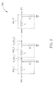
- FIG. 2 is a diagram illustrating an analog-to-digital converting device 200 according to another embodiment of the present invention.
- the integrator 202 comprises an operational amplifier 2022 and a capacitor 2024.
- the capacitor 2024 is coupled between the negative input terminal (-) of the operational amplifier 2022 and the output terminal of the operational amplifier 2022.
- the positive input terminal (+) of the operational amplifier 2022 is coupled to the common mode voltage Vcm of the operational amplifier 2022.
- the down-converted current signal Sdci is directly coupled to the negative input terminal (-) of the operational amplifier 2022.
- the first analog feedback signal Saf1 is feedback to the negative input terminal (-) of the operational amplifier 2022.
- the low-pass filter 304 comprises a plurality of LR (Inductor-resistor) filters 304_1-304_x, in which x is any positive integer number.
- the plurality of LR filters 304_1-304_x are connected in series in which the first LR filter 304_1 of the plurality of LR filters 304_1-304_x is arranged to receive the integrating signal Sint and the last LR filter 304_x of the plurality of LR filters 304_1-304_x is arranged to output the first filtered signal Sf1.
- Each LR filter of the plurality of LR filters 304_1-304_x comprises an inductor L and a resistor R, and the inductor L has a first terminal for receiving a pre-filtering signal and a second terminal for outputting a post-filtering signal and the resistor R has a first terminal coupled to the second terminal of the inductor L and a second terminal coupled to a reference voltage, i.e. the ground voltage Vgnd.
- the pre-filtering signal of the first LR filter 304_1 is the integrating signal Sint
- the post-filtering signal of the first LR filter 304_1 is the signal S_304_1.
- the pre-filtering signal of the second LR filter 304_2 is the signal S_304_1
- the post-filtering signal of the first LR filter 304_2 is the signal S_304_2, and so on.
- the low-pass filter 404 comprises a plurality of LC (Inductor-capacitor) filters 404_1-404_x, in which x is any positive integer number.
- the plurality of LR filters 404_1-404_x are connected in series in which the first LC filter 404_1 of the plurality of LC filters 404_1-404_x is arranged to receive the integrating signal Sint and the last LC filter 404_x of the plurality of LC filters 404_1-404_x is arranged to output the first filtered signal Sf1.
- Each LC filter of the plurality of LC filters 404_1-404_x comprises an inductor L and a capacitor C, and the inductor L has a first terminal for receiving a pre-filtering signal and a second terminal for outputting a post-filtering signal and the capacitor C has a first terminal coupled to the second terminal of the inductor L and a second terminal coupled to the ground voltage Vgnd.
- the pre-filtering signal of the first LC filter 404_1 is the integrating signal Sint
- the post-filtering signal of the first LC filter 404_1 is the signal S_404_1.
- the pre-filtering signal of the second LC filter 404_2 is the signal S_404_1
- the post-filtering signal of the first LC filter 404_2 is the signal S_404_2, and so on.
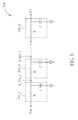
- the low-pass filter 504 comprises a plurality of RC (Resistor-capacitor) filters 504_1-504_x, in which x is any positive integer number.
- the plurality of RC filters 504_1-504_x are connected in series in which the first RC filter 504_1 of the plurality of RC filters 504_1-504_x is arranged to receive the integrating signal Sint and the last RC filter 504_x of the plurality of RC filters 504_1-504_x is arranged to output the first filtered signal Sf1.
- Each RC filter of the plurality of RC filters 504_1-504_x comprises an resistor R and a capacitor C, and the resistor R has a first terminal for receiving a pre-filtering signal and a second terminal for outputting a post-filtering signal and the capacitor C has a first terminal coupled to the second terminal of the resistor R and a second terminal coupled to the ground voltage Vgnd.
- the pre-filtering signal of the first RC filter 504_1 is the integrating signal Sint
- the post-filtering signal of the first RC filter 504_1 is the signal S_504_1.
- the pre-filtering signal of the second RC filter 504_2 is the signal S_504_1
- the post-filtering signal of the first RC filter 504_2 is the signal S_504_2, and so on.
- the low-pass filter 604 comprises a plurality of RC (Resistor-capacitor) filters 604_1-604_x, in which x is any positive integer number.
- the plurality of RC filters 604_1-604_x are connected in series in which the first RC filter 604_1 of the plurality of RC filters 604_1-604_x is arranged to receive the integrating signal Sint and the last RC filter 604_x of the plurality of RC filters 604_1-604_x is arranged to output the first filtered signal Sf1.
- Each RC filter of the plurality of RC filters 604-1-604-(x-1) comprises a resistor R, a capacitor C, and a buffer B.
- the resistor R has a first terminal for receiving a pre-filtering signal
- the capacitor C has a first terminal coupled to the second terminal of the resistor R and a second terminal coupled to the ground voltage Vgnd
- the buffer B is arranged for outputting a post-filtering signal. More specifically, the buffer B has an input terminal coupled to the second terminal of the resistor R and an output terminal for outputting the post-filtering signal.
- the pre-filtering signal of the first RC filter 604_1 is the integrating signal Sint
- the post-filtering signal of the first RC filter 604_1 is the signal S_604_1.
- the pre-filtering signal of the second RC filter 604_2 is the signal S_604_1
- the post-filtering signal of the first RC filter 604_2 is the signal S_604_2, and so on as shown in FIG. 6 .
- the last RC filter 604_x merely comprises one resistor R and one capacitor C, and the last RC filter 604_x is arranged for outputting the first filtered signal Sf1.
- the low-pass filter 704 comprises a plurality of RC (Resistor-capacitor) filters 704_1-704_x and a plurality of second DACs 705_1-705_x, in which x is any positive integer number.
- the plurality of RC filters 704_1-704_x are connected in series in which the first RC filter 704_1 of the plurality of RC filters 704_1-704_x is arranged to receive the integrating signal Sint and the last RC filter 704_x of the plurality of RC filters 704_1-704_x is arranged to output the first filtered signal Sf1.
- Each RC filter of the plurality of RC filters 704_1-704_x comprises an resistor R and a capacitor C, and the resistor R has a first terminal for receiving a pre-filtering signal and a second terminal for outputting a post-filtering signal and the capacitor C has a first terminal coupled to the second terminal of the resistor R and a second terminal coupled to the ground voltage Vgnd.
- the pre-filtering signal of the first RC filter 704_1 is the integrating signal Sint
- the post-filtering signal of the first RC filter 704_1 is the signal S_704_1.
- the pre-filtering signal of the second RC filter 704_2 is the signal S_704_1
- the post-filtering signal of the first RC filter 704_2 is the signal S_704_2, and so on.
- the plurality of second DACs 705_1-705_x are arranged for generating a plurality of feedback signals S_705_1- S_705_x according to the digital output signal Sdo respectively, and the plurality of feedback signals S_705_1- S_705_x are feedback to the plurality of second terminals of the plurality of resistors R respectively as shown in FIG. 7 .
- FIG. 8 is a first embodiment 806 of the ADC 106 according to the present invention.
- the ADC 806 is a continuous-time delta-sigma modulating ADC, and the ADC 806 comprises a loop filter 8061, a quantizer 8062, a delay circuit 8063, a first digital-to-analog converter (DAC) 8064, and a second DAC 8065.
- the loop filter 8061 is arranged to generate a second filtered signal Sf2 according to the first filtered signal Sf1 and a second analog feedback signal Saf2.
- the quantizer 8062 is arranged to generate the digital output signal Sdo according to the second filtered signal and a third analog feedback signal Saf3.
- the delay circuit 8063 is arranged to generate a delayed digital signal Sddo by delaying the digital output signal Sdo.
- the first DAC 8064 is arranged to generate the second analog feedback signal Saf2 according to the delayed digital signal Sddo.
- the second DAC 8065 is arranged to generate the third analog feedback signal Saf3 according to the delayed digital signal Sddo.
- the loop filter 8061 comprises a first resistor 8061a, a first operational amplifier 8061b, a first capacitor 8061c, a second operational amplifier 8061d, a second capacitor 8061e, a second resistor 8061f, a third capacitor 8061g, a third operational amplifier 8061h, and a fourth capacitor 8061i.
- the first resistor 8061a has a first terminal for receiving the first filtered signal Sf1.
- the first operational amplifier 8061b having a negative input terminal (-) coupled to a second terminal of the first resistor 8061a.
- the first capacitor 8061c has a first terminal coupled to the negative input terminal (-) of the first operational amplifier 8061b and a second terminal coupled to an output terminal of the first operational amplifier 8061b.
- the positive input terminal (+) of the first operational amplifier 8061b is coupled to the common mode voltage Vcm of the first operational amplifier 8061b.
- the second operational amplifier 8061d has a negative input terminal (-) coupled to the output terminal of the first operational amplifier 8061b.
- the second capacitor 8061e has a first terminal coupled to the negative input terminal (-) of the second operational amplifier 8061d and a second terminal coupled to an output terminal of the second operational amplifier 8061d.
- the positive input terminal (+) of the second operational amplifier 8061d is coupled to the common mode voltage Vcm of the second operational amplifier 8061d.
- the second resistor 8061f has a first terminal coupled to the negative input terminal (-) of the second operational amplifier 8061d and a second terminal coupled to the output terminal of the second operational amplifier 8061d.
- the third capacitor 8061g has a first terminal coupled to the negative input terminal (-) of the second operational amplifier 8061d and a second terminal coupled to the output terminal of the second operational amplifier 8061d.
- the third operational amplifier 8061h has a negative input terminal (-) coupled to the output terminal of the second operational amplifier 8061d.
- the fourth capacitor 8061i has a first terminal coupled to the negative input terminal (-) of the third operational amplifier 8061h and a second terminal coupled to an output terminal of the third operational amplifier 8061h.
- the positive input terminal (+) of the third operational amplifier 8061h is coupled to the common mode voltage Vcm of the third operational amplifier 8061h.
- the second analog feedback signal Saf2 is feedback to the negative input terminal (-) of the first operational amplifier 8061b, and the output terminal of the third operational amplifier 8061h is arranged to output the second filtered signal Sf2.
- the loop filter 8061 further comprises a combining circuit 8066 arranged to combine the second filtered signal Sf2 and the third analog feedback signal Saf3, and to generate a combining signal for the quantizer 8062.
- the quantizer 8062 is arranged to generate the digital output signal Sdo according to the combining signal.
- FIG. 9 is a second embodiment 906 of the ADC 106 according to the present invention.
- the ADC 906 is a continuous-time delta-sigma modulating ADC, and the ADC 906 comprises a loop filter 9061, a quantizer 9062, a first delay circuit 9063, a first digital-to-analog converter (DAC) 9064, a second delay circuit 9065, and a second DAC 9066.
- the loop filter 9061 is arranged to generate a second filtered signal Sf2' according to the first filtered signal Sf1, a second analog feedback signal Saf2', and a third analog feedback signal Saf3'.
- the quantizer 9062 is arranged to generate the digital output signal Sdo according to the second filtered signal Sf2' .
- the first delay circuit 9063 is arranged to generate a first delayed digital signal Sddo1 by delaying the digital output signal Sdo.
- the first DAC 9064 is arranged to generate the second analog feedback signal Saf2' according to the first delayed digital signal Sddo1.
- the second delay circuit 9065 is arranged to generate a second delayed digital signal Sddo2 by delaying the first delayed digital signal Sddo1.
- the second DAC 9066 is arranged to generate the third analog feedback signal Saf3' according to the second delayed digital signal Sddo2.
- the loop filter 9061 is a single-operational-amplifier resonator, and the loop filter 9061 comprises a first resistor 9061a, an operational amplifier 9061b, a first capacitor 9061c, a second capacitor 9061d, a second resistor 9061e, a third resistor 9061f, a fourth resistor 9061g, a fifth resistor 9061h, and a third capacitor 9061i.
- the first resistor 9061a has a first terminal for receiving the first filtered signal Sf1.
- the operational amplifier 9061b has a negative input terminal (-) coupled to a second terminal of the first resistor 9061a.
- the operational amplifier 9061b has a positive input terminal (+) coupled to a reference voltage, e.g.
- the first capacitor 9061c has a first terminal coupled to the negative input terminal (-) of the operational amplifier 9061b.
- the second capacitor 9061d has a first terminal coupled to a second terminal of the first capacitor 9061c and a second terminal coupled to an output terminal of the operational amplifier 9061b.
- the second resistor 9061e has a first terminal coupled to the second terminal of the first capacitor 9061c and a second terminal coupled to a reference voltage, e.g. the ground voltage.
- the third resistor 9061f has a first terminal coupled to the negative input terminal (-) of the operational amplifier 9061b.
- the fourth resistor 9061g has a first terminal coupled to a second terminal of the third resistor 9061f and a second terminal coupled to the output terminal of the operational amplifier 9061b.
- the fifth resistor 9061h has a first terminal coupled to the second terminal of the third resistor 9061f and a second terminal coupled to the ground voltage.
- the third capacitor 9061i has a first terminal coupled to the second terminal of the third resistor 9061f and a second terminal coupled to the ground voltage.
- the second analog feedback signal Saf2' and the third analog feedback signal Saf3' are feedback to the negative input terminal (-) of the operational amplifier 9061b, and the output terminal of the operational amplifier 9061b is arranged to output the second filtered signal Sf2'.
- FIG. 10 is a third embodiment 1006 of the ADC 106 according to the present invention.
- the ADC 1006 is a continuous-time delta-sigma modulating ADC, and the ADC 1006 comprises a loop filter 10061, a quantizer 10062, a first delay circuit 10063, a first digital-to-analog converter (DAC) 10064, a second delay circuit 10065, a second DAC 10066, a third delay circuit 10067, and a third DAC 10068.
- DAC digital-to-analog converter
- the loop filter 10061 is arranged to generate a second filtered signal Sf2" according to the first filtered signal Sf1, a second analog feedback signal Saf2'', a third analog feedback signal Saf3'', and a fourth analog feedback signal Saf4''.
- the quantizer 10062 is arranged to generate the digital output signal Sdo according to the second filtered signal Sf22''.
- the first delay circuit 10063 is arranged to generate a first delayed digital signal Sddo1'' by delaying the digital output signal Sdo.
- the first DAC 10064 is arranged to generate the second analog feedback signal Saf2'' according to the first delayed digital signal Sddo1''.
- the second delay circuit 10065 is arranged to generate a second delayed digital signal Sddo2'' by delaying the first delayed digital signal Sddo1''.
- the second DAC 10066 is arranged to generate the third analog feedback signal Saf3'' according to the second delayed digital signal Sddo2''.
- the third delay circuit 10067 is arranged to generate a third delayed digital signal Sddo3'' by delaying the second delayed digital signal Sddo2''.
- the third DAC 10068 is arranged to generate the fourth analog feedback signal Saf4'' according to the third delayed digital signal Sddo3''.
- the loop filter 10061 is a single-operational-amplifier resonator, and the loop filter 10061 is similar to the loop filter 9061. Thus, the detailed description of the loop filter 10061 is omitted here for brevity.
- the second analog feedback signal Saf2'', the third analog feedback signal Saf3'', and the fourth analog feedback signal Saf4'' are feedback to the negative input terminal (-) of the operational amplifier 10061b, and the output terminal of the operational amplifier 10061b is arranged to output the second filtered signal Sf2''.
- FIG. 11 is a fourth embodiment 1106 of the ADC 106 according to the present invention.
- the ADC 1106 is a continuous-time delta-sigma modulating ADC, and the ADC 1106 comprises a loop filter 11061, a quantizer 11062, a first delay circuit 11063, a first digital-to-analog converter (DAC) 11064, a second delay circuit 11065, and a second DAC 11066.
- the loop filter 11061 is arranged to generate a second filtered signal Sf2'' according to the first filtered signal Sf1, a second analog feedback signal Saf2''', and a third analog feedback signal Saf3''.
- the quantizer 11062 is arranged to generate the digital output signal Sdo according to the second filtered signal Sf2''' and the third analog feedback signal Saf3'''.
- the first delay circuit 11063 is arranged to generate a first delayed digital signal Sddo1''' by delaying the digital output signal Sdo.
- the first DAC 11064 is arranged to generate the third analog feedback signal Saf3''' according to the first delayed digital signal Sddo1'''.
- the second delay circuit 11065 is arranged to generate a second delayed digital signal Sddo2''' by delaying the first delayed digital signal Sddo1'''.
- the second DAC 11066 is arranged to generate the second analog feedback signal Saf2''' according to the second delayed digital signal Sddo2'''.
- the loop filter 11061 is a single-operational-amplifier resonator, and the loop filter 11061 is similar to the loop filter 9061. Thus, the detailed description of the loop filter 11061 is omitted here for brevity.
- the second analog feedback signal Saf2''' is feedback to the negative input terminal (-) of the operational amplifier 11061b, and the output terminal of the operational amplifier 11061b is arranged to output the second filtered signal Sf2'''.
- the third analog feedback signal Saf3'' is feedback to the output terminal of the operational amplifier 11061b, and the quantizer 11062 is arranged to output the digital output signal Sdo according to the second filtered signal Sf2''' and the third analog feedback signal Saf3'''.
- FIG. 3-FIG. 11 illustrate the different embodiments of the low-pass filter 104 and the ADC 106 respectively. Any combinations of the different embodiments can be applied into the low-pass filter 104 and the ADC 106 of the analog-to-digital converting device 100 or the analog-to-digital converting device 200.
- the order of the ADC 106 is also not limited to be the same as that shown in the above embodiments. As a person skilled in the art can readily understand details of the modified analog-to-digital converting devices after reading above paragraphs, further description is omitted here for brevity.
- FIG. 1-FIG. 11 have been simplified into the single-ended versions.
- the present analog-to-digital converting device may be implemented as fully-differential devices, and the fully-differential devices also have the similar characteristics and advantages.
- the fully-differential version of the analog-to-digital converting device the detailed description is omitted here for brevity.
- FIG. 12 is a flowchart illustrating an analog-to-digital converting method 1200 according to an embodiment of the present invention. Provided that substantially the same result is achieved, the steps of the flowchart shown in FIG. 12 need not be in the exact order shown and need not be contiguous, that is, other steps can be intermediate.
- the analog-to-digital converting method 1200 comprises: Step 1202: Generate the integrating signal Sint according to the analog input signal Sin and the first analog feedback signal Saf1; Step 1204: Low-pass filtering the integrating signal Sint to generate the first filtered signal Sf1; Step 1206: Generate the second filtered signal Sf2 according to the first filtered signal Sf1 and the second analog feedback signal Saf2; Step 1208: Generate the digital output signal Sdo at least according to the second filtered signal Sf2; Step 1210: Generate the second analog feedback signal Saf2 according to the digital output signal Sdo; and Step 1212: Generate the first analog feedback signal Saf1 according to the digital output signal Sdo.
- the low-pass filter 104, the ADC 106, the delay circuit 109, the first DAC 108, and the integrator 102 are configured to be a closed-loop circuit.
- the integrator 102 has high gain, the noise of ADC 106 can be greatly reduced when referred to the input of device 100. In other words, the specification requirement of the ADC 106 can be relaxed. As a result, the areas and powers of the present analog-to-digital converting device 100 and the analog-to-digital converting device 200 are reduced.
- the stability of ADC 106 is almost not affected. This is because the bandwidth of the low-pass filter 104 is much smaller than the bandwidth of the ADC 106. And when the ADC 106 receives the first filtered signal Sf1 generated by the circuit comprised of the first DAC 108, the integrator 102, and the low-pass filter 104, the bandwidth of the first filtered signal Sf1 is also very small in comparison to the bandwidth of the ADC 106. Thus, the ADC 106 can be kept stable.
- the noise level requirement of the ADC 106 is reduced, the specification requirement of the low-pass filter 104 (or 504) is relaxed. Then, the low-pass filter 104 can be designed to have large resistance and small capacitance to reduce the size area of the low-pass filter 104. Therefore, the area of the present analog-to-digital converting device 100 (or 200) is further reduced.
- the noise of the ADC 106 can be greatly reduced.
- the analog-to-digital converting device 100 can also be regarded as a filter even though the ADC 106 is incorporated therein.
- the signal transfer function (STF) of the analog-to-digital converting device 100 (or 200) is a 2 nd order signal transfer function while taking an example that the low-pass filter 104 is a 1 st order RC filter.
- the analog-to-digital converting device 100 (or 200) can be regarded as a 2 nd order filter.
- the noise transfer function (NTF) of the ADC 106 is increased by one order when the ADC 106 is incorporated into the filter loop.
- the ADC 106 has steeper noise-shaping effect in comparison to the conventional counterpart.
Landscapes
- Engineering & Computer Science (AREA)
- Theoretical Computer Science (AREA)
- Analogue/Digital Conversion (AREA)
- Compression, Expansion, Code Conversion, And Decoders (AREA)
Abstract
Description
- The present invention relates to an analog-to-digital converting device according to the pre-characterizing clause of
claim 1. - In a wireless communication system, an analog-to-digital converter (ADC) is used to convert an analog signal into a digital signal after the RF signal is received by an antenna. However, the antenna may also receive signals other than the wanted signal at the same time. Therefore, a filter is used to filter out the unwanted signal before the signal inputting to the ADC. Normally, a filter has larger area or larger power consumption also has better filtering effect, but this also means that the filter costs higher. If a filter having bad filtering effect is employed, then the ADC should have wider dynamic range such that the unwanted signal can be suppressed by the ADC. However, the dynamic range of the ADC is inversely proportional to the supply voltage of the ADC, and the supply voltage only becomes smaller in the modern semiconductor process. Another way to increase the dynamic range of the ADC is to reduce the noise floor of the ADC. However, this method may again increase the area and power consumption of the ADC because the ADC may be designed to have large capacitor and small resistor. Therefore, providing a filtering ADC for cost/area reduction is an urgent problem in the field of wireless communication system.
- This in mind, the present invention aims at providing an analog-to-digital converting device that is cost/area/power consumption efficiency compared to the conventional designs.
- This is achieved by an analog-to-digital converting device according to
claim 1. The dependent claims pertain to corresponding further developments and improvements. - As will be seen more clearly from the detailed description following below, the claimed analog-to-digital converting device comprises an integrator, a low-pass filter, an analog-to-digital converter, and a first digital-to-analog converter. The integrator is arranged to generate an integrating signal according to an analog input signal and a first analog feedback signal. The low-pass filter is arranged to generate a first filtered signal according to the integrating signal. The analog-to-digital converter is arranged to generate a digital output signal according to the first filtered signal. The first digital-to-analog converter is arranged to generate the first analog feedback signal according to the digital output signal.
- In the following, the invention is further illustrated by way of example, taking reference to the accompanying drawings. Thereof
- FIG. 1
- is a diagram illustrating an analog-to-digital converting device according to an embodiment of the present invention,
- FIG. 2
- is a diagram illustrating an analog-to-digital converting device according to another embodiment of the present invention,
- FIG. 3
- is a first embodiment of a low-pass filter according to the present invention,
- FIG. 4
- is a second embodiment of the low-pass filter according to the present invention,
- FIG. 5
- is a third embodiment of the low-pass filter according to the present invention,
- FIG. 6
- is a fourth embodiment of the low-pass filter according to the present invention,
- FIG. 7
- is a fifth embodiment of the low-pass filter according to the present invention,
- FIG. 8
- is a first embodiment of an ADC according to the present invention,
- FIG. 9
- is a second embodiment of the ADC according to the present invention,
- FIG. 10
- is a third embodiment of the ADC according to the present invention,
- FIG. 11
- is a fourth embodiment of the ADC according to the present invention, and
- FIG. 12
- is a flowchart illustrating an analog-to-digital converting method according to an embodiment of the present invention.
- Please refer to
FIG. 1 , which is a diagram illustrating an analog-to-digital converting device 100 according to an embodiment of the present invention. The analog-to-digital converting device 100 may be a filtering ADC (Filtering Analog-to-digital converter), for which a filter with analog input and digital output is available, and the filter may have fixed or variable gain depending on the design choices. The analog-to-digital converting device 100 comprises anintegrator 102, a low-pass filter 104, an analog-to-digital converter (ADC) 106, and a first digital-to-analog converter (DAC) 108. Theintegrator 102 is arranged to generate an integrating signal Sint according to an analog input signal Sin and a first analog feedback signal Saf1. The low-pass filter 104 is arranged to generate a first filtered signal Sf1 according to the integrating signal Sint. TheADC 106 is arranged to generate a digital output signal Sdo according to the first filtered signal Sf1. Thefirst DAC 108 is arranged to generate the first analog feedback signal Saf1 according to the digital output signal Sdo. The ADC 106 may be a flash ADC, a successive approximate ADC, a continuous-time delta-sigma ADC, or any other types of ADC. - It should be noted that a
delay circuit 109 may be included to delay the digital output signal Sdo for generating a delayed digital signal Sd. Then, thefirst DAC 108 generates the first analog feedback signal Saf1 according to the delayed digital signal Sd. - For illustration purposes,
FIG. 1 further includes amixer 110 and a trans-impedance circuit 112. Themixer 110 is arranged to down-convert a RF signal Srf received from an antenna (not shown) into a down-converted current signal Sdci according to an oscillating signal Sosc. The trans-impedance circuit 112 is arranged to convert the down-converted current signal Sdci into the analog input signal Sin. Therefore, the analog input signal Sin is a down-converted voltage signal in this embodiment. In this embodiment, theintegrator 102 comprises aresistor 1022, anoperational amplifier 1024, and acapacitor 1026. Theresistor 1022 has a first terminal coupled to the trans-impedance circuit 112 for receiving the analog input signal Sin. Theoperational amplifier 1024 has a negative input terminal (-) coupled to a second terminal of theresistor 1022, and an output terminal for outputting the integrating signal Sint. Thecapacitor 1026 has a first terminal coupled to the negative input terminal (-) of theoperational amplifier 1024 and a second terminal coupled to the output terminal of theoperational amplifier 1024. The first analog feedback signal Saf1 is feedback to the negative input terminal (-) of theoperational amplifier 1024. The positive input terminal (+) of theoperational amplifier 1024 is coupled to a common mode voltage Vcm of theoperational amplifier 1024. Theresistor 1022 may be an adjustable resistor. However, this is not a limitation of the present invention. The analog-to-digital convertingdevice 100 may be arranged to directly receive the down-converted current signal Sdci. If the analog-to-digital convertingdevice 100 is arranged to directly receive the down-converted current signal Sdci, then the trans-impedance circuit 112 and theresistor 1022 inFIG. 1 are discarded as shown inFIG. 2 . -
FIG. 2 is a diagram illustrating an analog-to-digital convertingdevice 200 according to another embodiment of the present invention. In this embodiment, theintegrator 202 comprises anoperational amplifier 2022 and acapacitor 2024. Thecapacitor 2024 is coupled between the negative input terminal (-) of theoperational amplifier 2022 and the output terminal of theoperational amplifier 2022. The positive input terminal (+) of theoperational amplifier 2022 is coupled to the common mode voltage Vcm of theoperational amplifier 2022. The down-converted current signal Sdci is directly coupled to the negative input terminal (-) of theoperational amplifier 2022. The first analog feedback signal Saf1 is feedback to the negative input terminal (-) of theoperational amplifier 2022. - Please refer to
FIG. 3 , which is afirst embodiment 304 of the low-pass filter 104 according to the present invention. The low-pass filter 304 comprises a plurality of LR (Inductor-resistor) filters 304_1-304_x, in which x is any positive integer number. The plurality of LR filters 304_1-304_x are connected in series in which the first LR filter 304_1 of the plurality of LR filters 304_1-304_x is arranged to receive the integrating signal Sint and the last LR filter 304_x of the plurality of LR filters 304_1-304_x is arranged to output the first filtered signal Sf1. Each LR filter of the plurality of LR filters 304_1-304_x comprises an inductor L and a resistor R, and the inductor L has a first terminal for receiving a pre-filtering signal and a second terminal for outputting a post-filtering signal and the resistor R has a first terminal coupled to the second terminal of the inductor L and a second terminal coupled to a reference voltage, i.e. the ground voltage Vgnd. For example, the pre-filtering signal of the first LR filter 304_1 is the integrating signal Sint, and the post-filtering signal of the first LR filter 304_1 is the signal S_304_1. The pre-filtering signal of the second LR filter 304_2 is the signal S_304_1, and the post-filtering signal of the first LR filter 304_2 is the signal S_304_2, and so on. - Please refer to
FIG. 4 , which is asecond embodiment 404 of the low-pass filter 104 according to the present invention. The low-pass filter 404 comprises a plurality of LC (Inductor-capacitor) filters 404_1-404_x, in which x is any positive integer number. The plurality of LR filters 404_1-404_x are connected in series in which the first LC filter 404_1 of the plurality of LC filters 404_1-404_x is arranged to receive the integrating signal Sint and the last LC filter 404_x of the plurality of LC filters 404_1-404_x is arranged to output the first filtered signal Sf1. Each LC filter of the plurality of LC filters 404_1-404_x comprises an inductor L and a capacitor C, and the inductor L has a first terminal for receiving a pre-filtering signal and a second terminal for outputting a post-filtering signal and the capacitor C has a first terminal coupled to the second terminal of the inductor L and a second terminal coupled to the ground voltage Vgnd. For example, the pre-filtering signal of the first LC filter 404_1 is the integrating signal Sint, and the post-filtering signal of the first LC filter 404_1 is the signal S_404_1. The pre-filtering signal of the second LC filter 404_2 is the signal S_404_1, and the post-filtering signal of the first LC filter 404_2 is the signal S_404_2, and so on. - Please refer to
FIG. 5 , which is athird embodiment 504 of the low-pass filter 104 according to the present invention. The low-pass filter 504 comprises a plurality of RC (Resistor-capacitor) filters 504_1-504_x, in which x is any positive integer number. The plurality of RC filters 504_1-504_x are connected in series in which the first RC filter 504_1 of the plurality of RC filters 504_1-504_x is arranged to receive the integrating signal Sint and the last RC filter 504_x of the plurality of RC filters 504_1-504_x is arranged to output the first filtered signal Sf1. Each RC filter of the plurality of RC filters 504_1-504_x comprises an resistor R and a capacitor C, and the resistor R has a first terminal for receiving a pre-filtering signal and a second terminal for outputting a post-filtering signal and the capacitor C has a first terminal coupled to the second terminal of the resistor R and a second terminal coupled to the ground voltage Vgnd. For example, the pre-filtering signal of the first RC filter 504_1 is the integrating signal Sint, and the post-filtering signal of the first RC filter 504_1 is the signal S_504_1. The pre-filtering signal of the second RC filter 504_2 is the signal S_504_1, and the post-filtering signal of the first RC filter 504_2 is the signal S_504_2, and so on. - Please refer to
FIG. 6 , which is afourth embodiment 604 of the low-pass filter 104 according to the present invention. The low-pass filter 604 comprises a plurality of RC (Resistor-capacitor) filters 604_1-604_x, in which x is any positive integer number. The plurality of RC filters 604_1-604_x are connected in series in which the first RC filter 604_1 of the plurality of RC filters 604_1-604_x is arranged to receive the integrating signal Sint and the last RC filter 604_x of the plurality of RC filters 604_1-604_x is arranged to output the first filtered signal Sf1. Each RC filter of the plurality of RC filters 604-1-604-(x-1) comprises a resistor R, a capacitor C, and a buffer B. In the plurality of RC filters 604_1-604_(x-1), the resistor R has a first terminal for receiving a pre-filtering signal, the capacitor C has a first terminal coupled to the second terminal of the resistor R and a second terminal coupled to the ground voltage Vgnd, and the buffer B is arranged for outputting a post-filtering signal. More specifically, the buffer B has an input terminal coupled to the second terminal of the resistor R and an output terminal for outputting the post-filtering signal. For example, the pre-filtering signal of the first RC filter 604_1 is the integrating signal Sint, and the post-filtering signal of the first RC filter 604_1 is the signal S_604_1. The pre-filtering signal of the second RC filter 604_2 is the signal S_604_1, and the post-filtering signal of the first RC filter 604_2 is the signal S_604_2, and so on as shown inFIG. 6 . It is noted that the last RC filter 604_x merely comprises one resistor R and one capacitor C, and the last RC filter 604_x is arranged for outputting the first filtered signal Sf1. - Please refer to
FIG. 7 , which is afifth embodiment 704 of the low-pass filter 104 according to the present invention. The low-pass filter 704 comprises a plurality of RC (Resistor-capacitor) filters 704_1-704_x and a plurality of second DACs 705_1-705_x, in which x is any positive integer number. The plurality of RC filters 704_1-704_x are connected in series in which the first RC filter 704_1 of the plurality of RC filters 704_1-704_x is arranged to receive the integrating signal Sint and the last RC filter 704_x of the plurality of RC filters 704_1-704_x is arranged to output the first filtered signal Sf1. Each RC filter of the plurality of RC filters 704_1-704_x comprises an resistor R and a capacitor C, and the resistor R has a first terminal for receiving a pre-filtering signal and a second terminal for outputting a post-filtering signal and the capacitor C has a first terminal coupled to the second terminal of the resistor R and a second terminal coupled to the ground voltage Vgnd. For example, the pre-filtering signal of the first RC filter 704_1 is the integrating signal Sint, and the post-filtering signal of the first RC filter 704_1 is the signal S_704_1. The pre-filtering signal of the second RC filter 704_2 is the signal S_704_1, and the post-filtering signal of the first RC filter 704_2 is the signal S_704_2, and so on. Moreover, the plurality of second DACs 705_1-705_x are arranged for generating a plurality of feedback signals S_705_1- S_705_x according to the digital output signal Sdo respectively, and the plurality of feedback signals S_705_1- S_705_x are feedback to the plurality of second terminals of the plurality of resistors R respectively as shown inFIG. 7 . - Please refer to
FIG. 8 , which is afirst embodiment 806 of theADC 106 according to the present invention. TheADC 806 is a continuous-time delta-sigma modulating ADC, and theADC 806 comprises aloop filter 8061, aquantizer 8062, adelay circuit 8063, a first digital-to-analog converter (DAC) 8064, and asecond DAC 8065. Theloop filter 8061 is arranged to generate a second filtered signal Sf2 according to the first filtered signal Sf1 and a second analog feedback signal Saf2. Thequantizer 8062 is arranged to generate the digital output signal Sdo according to the second filtered signal and a third analog feedback signal Saf3. Thedelay circuit 8063 is arranged to generate a delayed digital signal Sddo by delaying the digital output signal Sdo. Thefirst DAC 8064 is arranged to generate the second analog feedback signal Saf2 according to the delayed digital signal Sddo. Thesecond DAC 8065 is arranged to generate the third analog feedback signal Saf3 according to the delayed digital signal Sddo. - The
loop filter 8061 comprises afirst resistor 8061a, a firstoperational amplifier 8061b, afirst capacitor 8061c, a secondoperational amplifier 8061d, asecond capacitor 8061e, asecond resistor 8061f, athird capacitor 8061g, a thirdoperational amplifier 8061h, and afourth capacitor 8061i. Thefirst resistor 8061a has a first terminal for receiving the first filtered signal Sf1. The firstoperational amplifier 8061b having a negative input terminal (-) coupled to a second terminal of thefirst resistor 8061a. Thefirst capacitor 8061c has a first terminal coupled to the negative input terminal (-) of the firstoperational amplifier 8061b and a second terminal coupled to an output terminal of the firstoperational amplifier 8061b. The positive input terminal (+) of the firstoperational amplifier 8061b is coupled to the common mode voltage Vcm of the firstoperational amplifier 8061b. The secondoperational amplifier 8061d has a negative input terminal (-) coupled to the output terminal of the firstoperational amplifier 8061b. Thesecond capacitor 8061e has a first terminal coupled to the negative input terminal (-) of the secondoperational amplifier 8061d and a second terminal coupled to an output terminal of the secondoperational amplifier 8061d. The positive input terminal (+) of the secondoperational amplifier 8061d is coupled to the common mode voltage Vcm of the secondoperational amplifier 8061d. Thesecond resistor 8061f has a first terminal coupled to the negative input terminal (-) of the secondoperational amplifier 8061d and a second terminal coupled to the output terminal of the secondoperational amplifier 8061d. Thethird capacitor 8061g has a first terminal coupled to the negative input terminal (-) of the secondoperational amplifier 8061d and a second terminal coupled to the output terminal of the secondoperational amplifier 8061d. The thirdoperational amplifier 8061h has a negative input terminal (-) coupled to the output terminal of the secondoperational amplifier 8061d. Thefourth capacitor 8061i has a first terminal coupled to the negative input terminal (-) of the thirdoperational amplifier 8061h and a second terminal coupled to an output terminal of the thirdoperational amplifier 8061h. The positive input terminal (+) of the thirdoperational amplifier 8061h is coupled to the common mode voltage Vcm of the thirdoperational amplifier 8061h. - According to the embodiment, the second analog feedback signal Saf2 is feedback to the negative input terminal (-) of the first
operational amplifier 8061b, and the output terminal of the thirdoperational amplifier 8061h is arranged to output the second filtered signal Sf2. Moreover, theloop filter 8061 further comprises a combiningcircuit 8066 arranged to combine the second filtered signal Sf2 and the third analog feedback signal Saf3, and to generate a combining signal for thequantizer 8062. Thequantizer 8062 is arranged to generate the digital output signal Sdo according to the combining signal. - Please refer to
FIG. 9 , which is asecond embodiment 906 of theADC 106 according to the present invention. TheADC 906 is a continuous-time delta-sigma modulating ADC, and theADC 906 comprises aloop filter 9061, aquantizer 9062, afirst delay circuit 9063, a first digital-to-analog converter (DAC) 9064, asecond delay circuit 9065, and asecond DAC 9066. Theloop filter 9061 is arranged to generate a second filtered signal Sf2' according to the first filtered signal Sf1, a second analog feedback signal Saf2', and a third analog feedback signal Saf3'. Thequantizer 9062 is arranged to generate the digital output signal Sdo according to the second filtered signal Sf2' . Thefirst delay circuit 9063 is arranged to generate a first delayed digital signal Sddo1 by delaying the digital output signal Sdo. Thefirst DAC 9064 is arranged to generate the second analog feedback signal Saf2' according to the first delayed digital signal Sddo1. Thesecond delay circuit 9065 is arranged to generate a second delayed digital signal Sddo2 by delaying the first delayed digital signal Sddo1. Thesecond DAC 9066 is arranged to generate the third analog feedback signal Saf3' according to the second delayed digital signal Sddo2. - The
loop filter 9061 is a single-operational-amplifier resonator, and theloop filter 9061 comprises a first resistor 9061a, an operational amplifier 9061b, afirst capacitor 9061c, asecond capacitor 9061d, a second resistor 9061e, athird resistor 9061f, afourth resistor 9061g, afifth resistor 9061h, and a third capacitor 9061i. The first resistor 9061a has a first terminal for receiving the first filtered signal Sf1. The operational amplifier 9061b has a negative input terminal (-) coupled to a second terminal of the first resistor 9061a. The operational amplifier 9061b has a positive input terminal (+) coupled to a reference voltage, e.g. a common mode voltage or a ground voltage. Thefirst capacitor 9061c has a first terminal coupled to the negative input terminal (-) of the operational amplifier 9061b. Thesecond capacitor 9061d has a first terminal coupled to a second terminal of thefirst capacitor 9061c and a second terminal coupled to an output terminal of the operational amplifier 9061b. The second resistor 9061e has a first terminal coupled to the second terminal of thefirst capacitor 9061c and a second terminal coupled to a reference voltage, e.g. the ground voltage. Thethird resistor 9061f has a first terminal coupled to the negative input terminal (-) of the operational amplifier 9061b. Thefourth resistor 9061g has a first terminal coupled to a second terminal of thethird resistor 9061f and a second terminal coupled to the output terminal of the operational amplifier 9061b. Thefifth resistor 9061h has a first terminal coupled to the second terminal of thethird resistor 9061f and a second terminal coupled to the ground voltage. The third capacitor 9061i has a first terminal coupled to the second terminal of thethird resistor 9061f and a second terminal coupled to the ground voltage. - According to the embodiment, the second analog feedback signal Saf2' and the third analog feedback signal Saf3' are feedback to the negative input terminal (-) of the operational amplifier 9061b, and the output terminal of the operational amplifier 9061b is arranged to output the second filtered signal Sf2'.
- Please refer to
FIG. 10 , which is athird embodiment 1006 of theADC 106 according to the present invention. TheADC 1006 is a continuous-time delta-sigma modulating ADC, and theADC 1006 comprises aloop filter 10061, aquantizer 10062, afirst delay circuit 10063, a first digital-to-analog converter (DAC) 10064, asecond delay circuit 10065, asecond DAC 10066, athird delay circuit 10067, and athird DAC 10068. Theloop filter 10061 is arranged to generate a second filtered signal Sf2" according to the first filtered signal Sf1, a second analog feedback signal Saf2'', a third analog feedback signal Saf3'', and a fourth analog feedback signal Saf4''. Thequantizer 10062 is arranged to generate the digital output signal Sdo according to the second filtered signal Sf22''. Thefirst delay circuit 10063 is arranged to generate a first delayed digital signal Sddo1'' by delaying the digital output signal Sdo. Thefirst DAC 10064 is arranged to generate the second analog feedback signal Saf2'' according to the first delayed digital signal Sddo1''. Thesecond delay circuit 10065 is arranged to generate a second delayed digital signal Sddo2'' by delaying the first delayed digital signal Sddo1''. Thesecond DAC 10066 is arranged to generate the third analog feedback signal Saf3'' according to the second delayed digital signal Sddo2''. Thethird delay circuit 10067 is arranged to generate a third delayed digital signal Sddo3'' by delaying the second delayed digital signal Sddo2''. Thethird DAC 10068 is arranged to generate the fourth analog feedback signal Saf4'' according to the third delayed digital signal Sddo3''. - The
loop filter 10061 is a single-operational-amplifier resonator, and theloop filter 10061 is similar to theloop filter 9061. Thus, the detailed description of theloop filter 10061 is omitted here for brevity. - According to the embodiment, the second analog feedback signal Saf2'', the third analog feedback signal Saf3'', and the fourth analog feedback signal Saf4'' are feedback to the negative input terminal (-) of the
operational amplifier 10061b, and the output terminal of theoperational amplifier 10061b is arranged to output the second filtered signal Sf2''. - Please refer to
FIG. 11 , which is afourth embodiment 1106 of theADC 106 according to the present invention. TheADC 1106 is a continuous-time delta-sigma modulating ADC, and theADC 1106 comprises aloop filter 11061, aquantizer 11062, afirst delay circuit 11063, a first digital-to-analog converter (DAC) 11064, asecond delay circuit 11065, and asecond DAC 11066. Theloop filter 11061 is arranged to generate a second filtered signal Sf2'' according to the first filtered signal Sf1, a second analog feedback signal Saf2''', and a third analog feedback signal Saf3'''. Thequantizer 11062 is arranged to generate the digital output signal Sdo according to the second filtered signal Sf2''' and the third analog feedback signal Saf3'''. Thefirst delay circuit 11063 is arranged to generate a first delayed digital signal Sddo1''' by delaying the digital output signal Sdo. Thefirst DAC 11064 is arranged to generate the third analog feedback signal Saf3''' according to the first delayed digital signal Sddo1'''. Thesecond delay circuit 11065 is arranged to generate a second delayed digital signal Sddo2''' by delaying the first delayed digital signal Sddo1'''. Thesecond DAC 11066 is arranged to generate the second analog feedback signal Saf2''' according to the second delayed digital signal Sddo2'''. - The
loop filter 11061 is a single-operational-amplifier resonator, and theloop filter 11061 is similar to theloop filter 9061. Thus, the detailed description of theloop filter 11061 is omitted here for brevity. - According to the embodiment, the second analog feedback signal Saf2''' is feedback to the negative input terminal (-) of the
operational amplifier 11061b, and the output terminal of theoperational amplifier 11061b is arranged to output the second filtered signal Sf2'''. The third analog feedback signal Saf3''' is feedback to the output terminal of theoperational amplifier 11061b, and thequantizer 11062 is arranged to output the digital output signal Sdo according to the second filtered signal Sf2''' and the third analog feedback signal Saf3'''. - The above
FIG. 3-FIG. 11 illustrate the different embodiments of the low-pass filter 104 and theADC 106 respectively. Any combinations of the different embodiments can be applied into the low-pass filter 104 and theADC 106 of the analog-to-digital convertingdevice 100 or the analog-to-digital convertingdevice 200. The order of theADC 106 is also not limited to be the same as that shown in the above embodiments. As a person skilled in the art can readily understand details of the modified analog-to-digital converting devices after reading above paragraphs, further description is omitted here for brevity. - It should be noted that, for illustration purposes, the embodiments as shown in above
FIG. 1-FIG. 11 have been simplified into the single-ended versions. Those skilled in the art are appreciated to understand that, in practical, the present analog-to-digital converting device may be implemented as fully-differential devices, and the fully-differential devices also have the similar characteristics and advantages. As those skilled in the art are appreciated to understand the operation of the fully-differential version of the analog-to-digital converting device, the detailed description is omitted here for brevity. - In summary, the method of the above mentioned analog-to-digital converting
device 100 or the analog-to-digital convertingdevice 200 can be summarized into the steps ofFIG. 12. FIG. 12 is a flowchart illustrating an analog-to-digital convertingmethod 1200 according to an embodiment of the present invention. Provided that substantially the same result is achieved, the steps of the flowchart shown inFIG. 12 need not be in the exact order shown and need not be contiguous, that is, other steps can be intermediate. The analog-to-digital convertingmethod 1200 comprises:Step 1202: Generate the integrating signal Sint according to the analog input signal Sin and the first analog feedback signal Saf1; Step 1204: Low-pass filtering the integrating signal Sint to generate the first filtered signal Sf1; Step 1206: Generate the second filtered signal Sf2 according to the first filtered signal Sf1 and the second analog feedback signal Saf2; Step 1208: Generate the digital output signal Sdo at least according to the second filtered signal Sf2; Step 1210: Generate the second analog feedback signal Saf2 according to the digital output signal Sdo; and Step 1212: Generate the first analog feedback signal Saf1 according to the digital output signal Sdo. - Briefly, according to the above embodiments, the low-
pass filter 104, theADC 106, thedelay circuit 109, thefirst DAC 108, and theintegrator 102 are configured to be a closed-loop circuit. As theintegrator 102 has high gain, the noise ofADC 106 can be greatly reduced when referred to the input ofdevice 100. In other words, the specification requirement of theADC 106 can be relaxed. As a result, the areas and powers of the present analog-to-digital convertingdevice 100 and the analog-to-digital convertingdevice 200 are reduced. - Moreover, when the
ADC 106 is incorporated into the closed-loop circuit, the stability ofADC 106 is almost not affected. This is because the bandwidth of the low-pass filter 104 is much smaller than the bandwidth of theADC 106. And when theADC 106 receives the first filtered signal Sf1 generated by the circuit comprised of thefirst DAC 108, theintegrator 102, and the low-pass filter 104, the bandwidth of the first filtered signal Sf1 is also very small in comparison to the bandwidth of theADC 106. Thus, theADC 106 can be kept stable. - In addition, when the noise level requirement of the
ADC 106 is reduced, the specification requirement of the low-pass filter 104 (or 504) is relaxed. Then, the low-pass filter 104 can be designed to have large resistance and small capacitance to reduce the size area of the low-pass filter 104. Therefore, the area of the present analog-to-digital converting device 100 (or 200) is further reduced. - Accordingly, by incorporating the
ADC 106 into a filter loop (i.e. the circuit comprised of thedelay circuit 109, thefirst DAC 108, theintegrator 102, and the low-pass filter 104,), the noise of theADC 106 can be greatly reduced. - It should be noted that the analog-to-digital converting device 100 (or 200) can also be regarded as a filter even though the
ADC 106 is incorporated therein. According to one embodiment, the signal transfer function (STF) of the analog-to-digital converting device 100 (or 200) is a 2nd order signal transfer function while taking an example that the low-pass filter 104 is a 1st order RC filter. Thus, the analog-to-digital converting device 100 (or 200) can be regarded as a 2nd order filter. Meanwhile, the noise transfer function (NTF) of theADC 106 is increased by one order when theADC 106 is incorporated into the filter loop. Thus, theADC 106 has steeper noise-shaping effect in comparison to the conventional counterpart. - All combinations and sub-combinations of above-described features also belong to the invention.
Claims (15)
- An analog-to-digital converting device (100, 200), characterized by:an integrator (102, 202), arranged to generate an integrating signal according to an analog input signal and a first analog feedback signal;a low-pass filter (104, 304, 404, 504, 604, 704), arranged to generate a first filtered signal according to the integrating signal;an analog-to-digital converter (106), arranged to generate a digital output signal according to the first filtered signal; anda first digital-to-analog converter (108), arranged to generate the first analog feedback signal according to the digital output signal.
- The analog-to-digital converting device (100) of claim 1, characterized by:a delay circuit (109), arranged to generate a delayed digital signal by delaying the digital output signal;wherein the first digital-to-analog converter (108) generates the first analog feedback signal according to the delayed digital signal.
- The analog-to-digital converting device (100) of claim 1, characterized in that the analog input signal is a down-converted voltage signal; and
the integrator (102) comprises:a resistor (1022), having a first terminal for receiving the analog input signal;an operational amplifier (1024), having an input terminal coupled to a second terminal of the resistor (1022), and an output terminal for outputting the integrating signal; anda capacitor (1026), having a first terminal coupled to the input terminal of the operational amplifier (1024) and a second terminal coupled to the output terminal of the operational amplifier (1024);wherein the first analog feedback signal is feedback to the input terminal of the operational amplifier (1024). - The analog-to-digital converting device (200) of claim 1, characterized in that the analog input signal is a down-converted current signal, and the integrator (202) comprises:an operational amplifier (2022), having an input terminal for receiving the analog input signal, and an output terminal for outputting the integrating signal; anda capacitor (2024), having a first terminal coupled to the input terminal of the operational amplifier (2022)and a second terminal coupled to the output terminal of the operational amplifier (2022);wherein the first analog feedback signal is feedback to the input terminal of the operational amplifier (2022).
- The analog-to-digital converting device (100, 200) of claim 1, characterized in that the low-pass filter (104, 304) comprises:a plurality of LR filters (304_1 - 304_x), the plurality of LR filters (304_1 - 304_x) are connected in series in which the first LR filter (304_1) of the plurality of LR filters (304_1 - 304_x) is arranged to receive the integrating signal and the last LR filter (304_x) of the plurality of LR filters (304_1 - 304_x) is arranged to output the first filtered signal.
- The analog-to-digital converting device (100, 200) of claim 1, characterized in that the low-pass filter (104, 404) comprises:a plurality of LC (404_1 - 404_x) filters, the plurality of LC filters (404_1 - 404_x) are connected in series in which the first LC filter (404_1) of the plurality of LC filters (404_1 - 404_x) is arranged to receive the integrating signal and the last LC filter (404_x) of the plurality of LR filters (404_1 - 404_x) is arranged to output the first filtered signal.
- The analog-to-digital converting device (100, 200) of claim 1, characterized in that the low-pass filter (104, 504) comprises:a plurality of RC (504_1 - 504_x) filters, the plurality of RC filters (504_1 - 504_x) are connected in series in which the first RC filter (504_1) of the plurality of RC filters (504_1 - 504_x) is arranged to receive the integrating signal and the last RC filter (504_x) of the plurality of RC filters (504_1 - 504_x) is arranged to output the first filtered signal.
- The analog-to-digital converting device (100, 200) of claim 7, characterized in that at least one RC filter of the plurality of RC filters (504_1 - 504_x) comprises:a buffer, for outputing a post-filtering signal to a next RC filter of the plurality of RC filters (504_1-504_x).
- The analog-to-digital converting device (100, 200) of claim 7, characterized by:a plurality of second digital-to-analog converters (705_1-705_x), for generating a plurality of feedback signals according to the digital output signal respectively;wherein the plurality of feedback signals are feedback into the plurality of the RC filters (504_1 - 504_x) respectively.
- The analog-to-digital converting device (100, 200) of claim 1, characterized in that the analog-to-digital converter (106) is a flash ADC, a successive approximate ADC, or a continuous-time delta-sigma ADC (806, 906, 1006, 1106).
- The analog-to-digital converting device (100, 200) of claim 1, characterized in that the analog-to-digital converter (806, 906, 1006, 1106) comprises:a loop filter (8061, 9061, 1061, 11061), arranged to generate a second filtered signal according to the first filtered signal and a second analog feedback signal;a quantizer (8062, 9062, 1062, 11062), arranged to generate the digital output signal at least according to the second filtered signal; anda second digital-to-analog converter (8064, 9064, 1064, 11064), arranged to generate the second analog feedback signal according to the digital output signal.
- The analog-to-digital converting device (100, 200) of claim 11, characterized in that the analog-to-digital converter (806, 906, 1006, 1106) further comprises:a first delay circuit (8063, 9063, 1063, 11063), arranged to generate a first delayed digital signal by delaying the digital output signal;wherein the second digital-to-analog converter (8064, 9064, 1064, 11064) generates the second analog feedback signal according to the first delayed digital signal.
- The analog-to-digital converting device (100, 200) of claim 12, characterized in that the analog-to-digital converter (906, 1006, 1106) further comprises:a second delay circuit (9065, 10065), arranged to generate a second delayed digital signal by delaying the first delayed digital signal; anda third digital-to-analog converter (9066, 10066), arranged to generate a third analog feedback signal according to the second delayed digital signal;wherein the third analog feedback signal is feedback to the loop filter (9061, 10061), and the loop filter (9061, 10061) generates the second filtered signal according to the first filtered signal, the second analog feedback signal, and the third analog feedback signal.
- The analog-to-digital converting device (100, 200) of claim 12, characterized in that the analog-to-digital converter further comprises:a third digital-to-analog converter, arranged to generate a third analog feedback signal according to the first delayed digital signal;wherein the third analog feedback signal is feedback to the quantizer, and the quantizer is arranged to generate the digital output signal according to the second filtered signal and the third analog feedback signal.
- The analog-to-digital converting device (100, 200) of claim 12, characterized in that the analog-to-digital converter (1106) further comprises:a second delay circuit (11065), arranged to generate a second delayed digital signal by delaying the digital output signal;a third digital-to-analog converter (11066), arranged to generate a third analog feedback signal according to the second delayed digital signal;wherein the third analog feedback signal is feedback to the quantizer (11062), and the quantizer (11062) is arranged to generate the digital output signal according to the second filtered signal and the third analog feedback signal.
Applications Claiming Priority (2)
| Application Number | Priority Date | Filing Date | Title |
|---|---|---|---|
| US201361914967P | 2013-12-12 | 2013-12-12 | |
| US14/540,041 US9184754B2 (en) | 2013-12-12 | 2014-11-13 | Analog-to-digital converting device and analog-to-digital converting method |
Publications (1)
| Publication Number | Publication Date |
|---|---|
| EP2890015A1 true EP2890015A1 (en) | 2015-07-01 |
Family
ID=52015986
Family Applications (1)
| Application Number | Title | Priority Date | Filing Date |
|---|---|---|---|
| EP14197322.2A Ceased EP2890015A1 (en) | 2013-12-12 | 2014-12-11 | Analog-to-digital converting device |
Country Status (3)
| Country | Link |
|---|---|
| US (1) | US9184754B2 (en) |
| EP (1) | EP2890015A1 (en) |
| CN (2) | CN104716959B (en) |
Families Citing this family (4)
| Publication number | Priority date | Publication date | Assignee | Title |
|---|---|---|---|---|
| US9419642B1 (en) * | 2015-06-11 | 2016-08-16 | Analog Devices, Inc. | Ultra low power dual quantizer architecture for oversampling delta-sigma modulator |
| US10461770B2 (en) * | 2017-07-13 | 2019-10-29 | Analog Devices Global Unlimited Company | Techniques for configurable ADC front-end RC filter |
| CN112097902B (en) * | 2019-12-03 | 2023-08-11 | 义明科技股份有限公司 | Optical sensor and sensing method thereof |
| US12015426B2 (en) * | 2022-08-04 | 2024-06-18 | Nxp B.V. | System and method of reducing delta-sigma modulator error using force-and-correction |
Citations (8)
| Publication number | Priority date | Publication date | Assignee | Title |
|---|---|---|---|---|
| US4467291A (en) * | 1981-11-23 | 1984-08-21 | U.S. Philips Corporation | Delta modulator having optimized loop filter |
| US20050116850A1 (en) * | 2003-10-31 | 2005-06-02 | Rahmi Hezar | Continuous time fourth order delta sigma analog-to-digital converter |
| US20090325632A1 (en) * | 2008-06-30 | 2009-12-31 | Simone Gambini | Loop delay compensation for continuous time sigma delta analog to digital converter |
| US20100219998A1 (en) * | 2009-02-27 | 2010-09-02 | Freescale Semiconductor, Inc. | Sigma-delta modulator with digitally filtered delay compensation |
| EP2273682A1 (en) * | 2008-04-28 | 2011-01-12 | Panasonic Corporation | Integrator, resonator, and oversampling a/d converter |
| US20110254718A1 (en) * | 2009-01-08 | 2011-10-20 | Panasonic Corporation | Integrator and delta-sigma modulator including the same |
| US8044836B2 (en) * | 2009-10-30 | 2011-10-25 | Stmicroelectronics Design & Application Gmbh | Continuous time sigma-delta A/D converter and electrical system comprising the A/D converter |
| US8171335B2 (en) * | 2008-09-16 | 2012-05-01 | Mediatek Inc. | Clock timing calibration circuit and clock timing calibration method for calibrating phase difference between different clock signals and related analog-to-digital conversion system using the same |
Family Cites Families (14)
| Publication number | Priority date | Publication date | Assignee | Title |
|---|---|---|---|---|
| JPS63289246A (en) * | 1987-05-20 | 1988-11-25 | Toyota Motor Corp | Suction pressure signal processing method for internal combustion engine |
| TWI253235B (en) * | 2004-03-19 | 2006-04-11 | Silicon Integrated Sys Corp | Background-calibrating pipelined analog-to-digital converter |
| US7277032B2 (en) * | 2005-10-21 | 2007-10-02 | Realtek Semiconductor Corp. | Low-pass filter based delta-sigma modulator |
| US7423567B2 (en) * | 2006-09-12 | 2008-09-09 | Cirrus Logic, Inc. | Analog-to-digital converter (ADC) having a reduced number of quantizer output levels |
| US7679540B2 (en) * | 2007-11-30 | 2010-03-16 | Infineon Technologies Ag | Double sampling DAC and integrator |
| CN101324642B (en) * | 2008-07-08 | 2011-06-08 | 奇瑞汽车股份有限公司 | Method and device for collecting multi-channel electromagnetic valve current |
| US7893855B2 (en) * | 2008-09-16 | 2011-02-22 | Mediatek Inc. | Delta-sigma analog-to-digital converter |
| CN101803200A (en) | 2008-10-06 | 2010-08-11 | 松下电器产业株式会社 | Differential switch, D/A converter, semiconductor integrated circuit, and communication apparatus |
| US7948414B2 (en) * | 2009-08-09 | 2011-05-24 | Mediatek, Inc. | Delta-sigma analog-to-digital conversion apparatus and method thereof |
| US8018365B1 (en) * | 2010-03-14 | 2011-09-13 | Mediatek Inc. | Continuous-time delta-sigma ADC with compact structure |
| CN103299549B (en) * | 2010-12-03 | 2016-11-09 | 马维尔国际贸易有限公司 | There is the analog-digital converter of noise reduction feedback network |
| JP2013038509A (en) | 2011-08-04 | 2013-02-21 | Sony Corp | Automatic variable step attenuator, and radio communication device |
| CN102386929B (en) * | 2011-09-22 | 2013-11-13 | 北京大学 | Sigma-Delta modulator and Sigma-Delta analog to digital converter comprising same |
| US8791848B2 (en) * | 2012-02-22 | 2014-07-29 | Mediatek Inc. | Sigma-delta modulators with excess loop delay compensation |
-
2014
- 2014-11-13 US US14/540,041 patent/US9184754B2/en active Active
- 2014-12-08 CN CN201410745152.4A patent/CN104716959B/en active Active
- 2014-12-08 CN CN201810199355.6A patent/CN108336998B/en active Active
- 2014-12-11 EP EP14197322.2A patent/EP2890015A1/en not_active Ceased
Patent Citations (8)
| Publication number | Priority date | Publication date | Assignee | Title |
|---|---|---|---|---|
| US4467291A (en) * | 1981-11-23 | 1984-08-21 | U.S. Philips Corporation | Delta modulator having optimized loop filter |
| US20050116850A1 (en) * | 2003-10-31 | 2005-06-02 | Rahmi Hezar | Continuous time fourth order delta sigma analog-to-digital converter |
| EP2273682A1 (en) * | 2008-04-28 | 2011-01-12 | Panasonic Corporation | Integrator, resonator, and oversampling a/d converter |
| US20090325632A1 (en) * | 2008-06-30 | 2009-12-31 | Simone Gambini | Loop delay compensation for continuous time sigma delta analog to digital converter |
| US8171335B2 (en) * | 2008-09-16 | 2012-05-01 | Mediatek Inc. | Clock timing calibration circuit and clock timing calibration method for calibrating phase difference between different clock signals and related analog-to-digital conversion system using the same |
| US20110254718A1 (en) * | 2009-01-08 | 2011-10-20 | Panasonic Corporation | Integrator and delta-sigma modulator including the same |
| US20100219998A1 (en) * | 2009-02-27 | 2010-09-02 | Freescale Semiconductor, Inc. | Sigma-delta modulator with digitally filtered delay compensation |
| US8044836B2 (en) * | 2009-10-30 | 2011-10-25 | Stmicroelectronics Design & Application Gmbh | Continuous time sigma-delta A/D converter and electrical system comprising the A/D converter |
Non-Patent Citations (2)
| Title |
|---|
| GERHARD MITTEREGGER ET AL: "A 20-mW 640-MHz CMOS Continuous-Time ADC With 20-MHz Signal Bandwidth, 80-dB Dynamic Range and 12-bit ENOB", IEEE JOURNAL OF SOLID-STATE CIRCUITS, IEEE SERVICE CENTER, PISCATAWAY, NJ, USA, vol. 41, no. 12, 1 December 2006 (2006-12-01), pages 2641 - 2649, XP011150731, ISSN: 0018-9200, DOI: 10.1109/JSSC.2006.884332 * |
| KELLER M ET AL: "A Comparative Study on Excess-Loop-Delay Compensation Techniques for Continuous-Time Sigma-Delta Modulators", IEEE TRANSACTIONS ON CIRCUITS AND SYSTEMS I: REGULAR PAPERS, IEEE, US, vol. 55, no. 11, 1 December 2008 (2008-12-01), pages 3480 - 3487, XP011333313, ISSN: 1549-8328, DOI: 10.1109/TCSI.2008.925362 * |
Also Published As
| Publication number | Publication date |
|---|---|
| US9184754B2 (en) | 2015-11-10 |
| CN104716959B (en) | 2018-04-13 |
| US20150171877A1 (en) | 2015-06-18 |
| CN104716959A (en) | 2015-06-17 |
| CN108336998B (en) | 2021-11-30 |
| CN108336998A (en) | 2018-07-27 |
Similar Documents
| Publication | Publication Date | Title |
|---|---|---|
| US9564916B2 (en) | Suppressing signal transfer function peaking in a feedforward delta sigma converter | |
| US8570200B2 (en) | Continuous-time oversampled converter having enhanced immunity to noise | |
| JP5754550B2 (en) | ΔΣ modulator and ΔΣ A / D converter | |
| US9019136B2 (en) | Sigma-delta modulators with high speed feed-forward architecture | |
| US8502719B2 (en) | Continuous-time oversampled converter having passive filter | |
| US8570201B2 (en) | Direct feedback for continuous-time oversampled converters | |
| US10491237B1 (en) | Continuous-time delta-sigma modulator | |
| US10541706B2 (en) | Dynamic-zoom analog to digital converter (ADC) having a coarse flash ADC and a fine passive single-bit modulator | |
| JP4875767B2 (en) | Integrator, resonator and oversampling A / D converter | |
| US9948318B1 (en) | Delta-sigma modulator and method for enhancing stability of delta-sigma modulator | |
| TWI738335B (en) | Amplifier, operating method thereof and amplifier circuit | |
| Billa et al. | 15.4 A 280µW 24kHz-BW 98.5 dB-SNDR chopped single-bit CT ΔΣM achieving< 10Hz 1/f noise corner without chopping artifacts | |
| US9793908B2 (en) | Protection circuits for tunable resistor at continuous-time ADC input | |
| US9184754B2 (en) | Analog-to-digital converting device and analog-to-digital converting method | |
| JPH04233332A (en) | Analog-digital converter | |
| Choi et al. | A 101-dB SNR hybrid delta-sigma audio ADC using post integration time control | |
| Aiba et al. | A fifth-order gm–c continuous-time Δ Σ modulator with process-insensitive input linear range | |
| Yu et al. | Bandpass sigma–delta modulator employing SAW resonator as loop filter | |
| Sharma et al. | A 6b 800ms/s 3.62 mw nyquist ac-coupled VCO-based ADC in 65nm CMOS | |
| Suanes et al. | A 0.8 mW 50kHz 94.6 dB-SNDR bootstrapping-free SC delta-sigma modulator ADC with flicker noise cancellation | |
| JP5031705B2 (en) | DC offset removal circuit and receiver | |
| JP2011077689A (en) | Integrator and oversampling a-d converter including the same | |
| JP4071211B2 (en) | Delta-sigma modulator, 1-bit amplifier | |
| Lin et al. | A continuous-time delta-sigma modulator using feedback resistors | |
| Yu et al. | Electromechanical-Filter-Based Bandpass Sigma–Delta Modulator |
Legal Events
| Date | Code | Title | Description |
|---|---|---|---|
| PUAI | Public reference made under article 153(3) epc to a published international application that has entered the european phase |
Free format text: ORIGINAL CODE: 0009012 |
|
| 17P | Request for examination filed |
Effective date: 20141211 |
|
| AK | Designated contracting states |
Kind code of ref document: A1 Designated state(s): AL AT BE BG CH CY CZ DE DK EE ES FI FR GB GR HR HU IE IS IT LI LT LU LV MC MK MT NL NO PL PT RO RS SE SI SK SM TR |
|
| AX | Request for extension of the european patent |
Extension state: BA ME |
|
| R17P | Request for examination filed (corrected) |
Effective date: 20150806 |
|
| RBV | Designated contracting states (corrected) |
Designated state(s): AL AT BE BG CH CY CZ DE DK EE ES FI FR GB GR HR HU IE IS IT LI LT LU LV MC MK MT NL NO PL PT RO RS SE SI SK SM TR |
|
| 17Q | First examination report despatched |
Effective date: 20171130 |
|
| STAA | Information on the status of an ep patent application or granted ep patent |
Free format text: STATUS: THE APPLICATION HAS BEEN REFUSED |
|
| 18R | Application refused |
Effective date: 20190527 |