EP2889874B1 - Wireless display sink device - Google Patents
Wireless display sink device Download PDFInfo
- Publication number
- EP2889874B1 EP2889874B1 EP14197886.6A EP14197886A EP2889874B1 EP 2889874 B1 EP2889874 B1 EP 2889874B1 EP 14197886 A EP14197886 A EP 14197886A EP 2889874 B1 EP2889874 B1 EP 2889874B1
- Authority
- EP
- European Patent Office
- Prior art keywords
- signal
- decoder
- display panel
- wireless
- video
- Prior art date
- Legal status (The legal status is an assumption and is not a legal conclusion. Google has not performed a legal analysis and makes no representation as to the accuracy of the status listed.)
- Active
Links
Images





Classifications
-
- H—ELECTRICITY
- H04—ELECTRIC COMMUNICATION TECHNIQUE
- H04N—PICTORIAL COMMUNICATION, e.g. TELEVISION
- H04N21/00—Selective content distribution, e.g. interactive television or video on demand [VOD]
- H04N21/40—Client devices specifically adapted for the reception of or interaction with content, e.g. set-top-box [STB]; Operations thereof
- H04N21/41—Structure of client; Structure of client peripherals
- H04N21/4104—Peripherals receiving signals from specially adapted client devices
- H04N21/4122—Peripherals receiving signals from specially adapted client devices additional display device, e.g. video projector
-
- H—ELECTRICITY
- H04—ELECTRIC COMMUNICATION TECHNIQUE
- H04N—PICTORIAL COMMUNICATION, e.g. TELEVISION
- H04N5/00—Details of television systems
- H04N5/44—Receiver circuitry for the reception of television signals according to analogue transmission standards
- H04N5/46—Receiver circuitry for the reception of television signals according to analogue transmission standards for receiving on more than one standard at will
-
- G—PHYSICS
- G09—EDUCATION; CRYPTOGRAPHY; DISPLAY; ADVERTISING; SEALS
- G09G—ARRANGEMENTS OR CIRCUITS FOR CONTROL OF INDICATING DEVICES USING STATIC MEANS TO PRESENT VARIABLE INFORMATION
- G09G3/00—Control arrangements or circuits, of interest only in connection with visual indicators other than cathode-ray tubes
- G09G3/20—Control arrangements or circuits, of interest only in connection with visual indicators other than cathode-ray tubes for presentation of an assembly of a number of characters, e.g. a page, by composing the assembly by combination of individual elements arranged in a matrix no fixed position being assigned to or needed to be assigned to the individual characters or partial characters
-
- G—PHYSICS
- G09—EDUCATION; CRYPTOGRAPHY; DISPLAY; ADVERTISING; SEALS
- G09G—ARRANGEMENTS OR CIRCUITS FOR CONTROL OF INDICATING DEVICES USING STATIC MEANS TO PRESENT VARIABLE INFORMATION
- G09G5/00—Control arrangements or circuits for visual indicators common to cathode-ray tube indicators and other visual indicators
- G09G5/003—Details of a display terminal, the details relating to the control arrangement of the display terminal and to the interfaces thereto
- G09G5/006—Details of the interface to the display terminal
-
- G—PHYSICS
- G09—EDUCATION; CRYPTOGRAPHY; DISPLAY; ADVERTISING; SEALS
- G09G—ARRANGEMENTS OR CIRCUITS FOR CONTROL OF INDICATING DEVICES USING STATIC MEANS TO PRESENT VARIABLE INFORMATION
- G09G3/00—Control arrangements or circuits, of interest only in connection with visual indicators other than cathode-ray tubes
- G09G3/20—Control arrangements or circuits, of interest only in connection with visual indicators other than cathode-ray tubes for presentation of an assembly of a number of characters, e.g. a page, by composing the assembly by combination of individual elements arranged in a matrix no fixed position being assigned to or needed to be assigned to the individual characters or partial characters
- G09G3/34—Control arrangements or circuits, of interest only in connection with visual indicators other than cathode-ray tubes for presentation of an assembly of a number of characters, e.g. a page, by composing the assembly by combination of individual elements arranged in a matrix no fixed position being assigned to or needed to be assigned to the individual characters or partial characters by control of light from an independent source
- G09G3/3406—Control of illumination source
-
- G—PHYSICS
- G09—EDUCATION; CRYPTOGRAPHY; DISPLAY; ADVERTISING; SEALS
- G09G—ARRANGEMENTS OR CIRCUITS FOR CONTROL OF INDICATING DEVICES USING STATIC MEANS TO PRESENT VARIABLE INFORMATION
- G09G3/00—Control arrangements or circuits, of interest only in connection with visual indicators other than cathode-ray tubes
- G09G3/20—Control arrangements or circuits, of interest only in connection with visual indicators other than cathode-ray tubes for presentation of an assembly of a number of characters, e.g. a page, by composing the assembly by combination of individual elements arranged in a matrix no fixed position being assigned to or needed to be assigned to the individual characters or partial characters
- G09G3/34—Control arrangements or circuits, of interest only in connection with visual indicators other than cathode-ray tubes for presentation of an assembly of a number of characters, e.g. a page, by composing the assembly by combination of individual elements arranged in a matrix no fixed position being assigned to or needed to be assigned to the individual characters or partial characters by control of light from an independent source
- G09G3/36—Control arrangements or circuits, of interest only in connection with visual indicators other than cathode-ray tubes for presentation of an assembly of a number of characters, e.g. a page, by composing the assembly by combination of individual elements arranged in a matrix no fixed position being assigned to or needed to be assigned to the individual characters or partial characters by control of light from an independent source using liquid crystals
- G09G3/3611—Control of matrices with row and column drivers
-
- H—ELECTRICITY
- H04—ELECTRIC COMMUNICATION TECHNIQUE
- H04N—PICTORIAL COMMUNICATION, e.g. TELEVISION
- H04N19/00—Methods or arrangements for coding, decoding, compressing or decompressing digital video signals
- H04N19/44—Decoders specially adapted therefor, e.g. video decoders which are asymmetric with respect to the encoder
-
- H—ELECTRICITY
- H04—ELECTRIC COMMUNICATION TECHNIQUE
- H04N—PICTORIAL COMMUNICATION, e.g. TELEVISION
- H04N21/00—Selective content distribution, e.g. interactive television or video on demand [VOD]
- H04N21/40—Client devices specifically adapted for the reception of or interaction with content, e.g. set-top-box [STB]; Operations thereof
- H04N21/41—Structure of client; Structure of client peripherals
- H04N21/422—Input-only peripherals, i.e. input devices connected to specially adapted client devices, e.g. global positioning system [GPS]
- H04N21/42204—User interfaces specially adapted for controlling a client device through a remote control device; Remote control devices therefor
-
- H—ELECTRICITY
- H04—ELECTRIC COMMUNICATION TECHNIQUE
- H04N—PICTORIAL COMMUNICATION, e.g. TELEVISION
- H04N21/00—Selective content distribution, e.g. interactive television or video on demand [VOD]
- H04N21/40—Client devices specifically adapted for the reception of or interaction with content, e.g. set-top-box [STB]; Operations thereof
- H04N21/43—Processing of content or additional data, e.g. demultiplexing additional data from a digital video stream; Elementary client operations, e.g. monitoring of home network or synchronising decoder's clock; Client middleware
- H04N21/436—Interfacing a local distribution network, e.g. communicating with another STB or one or more peripheral devices inside the home
- H04N21/4363—Adapting the video stream to a specific local network, e.g. a Bluetooth® network
- H04N21/43637—Adapting the video stream to a specific local network, e.g. a Bluetooth® network involving a wireless protocol, e.g. Bluetooth®, RF or wireless LAN [IEEE 802.11]
-
- H—ELECTRICITY
- H04—ELECTRIC COMMUNICATION TECHNIQUE
- H04N—PICTORIAL COMMUNICATION, e.g. TELEVISION
- H04N5/00—Details of television systems
- H04N5/44—Receiver circuitry for the reception of television signals according to analogue transmission standards
- H04N5/60—Receiver circuitry for the reception of television signals according to analogue transmission standards for the sound signals
- H04N5/602—Receiver circuitry for the reception of television signals according to analogue transmission standards for the sound signals for digital sound signals
-
- H—ELECTRICITY
- H04—ELECTRIC COMMUNICATION TECHNIQUE
- H04N—PICTORIAL COMMUNICATION, e.g. TELEVISION
- H04N5/00—Details of television systems
- H04N5/74—Projection arrangements for image reproduction, e.g. using eidophor
- H04N5/7408—Direct viewing projectors, e.g. an image displayed on a video CRT or LCD display being projected on a screen
-
- G—PHYSICS
- G09—EDUCATION; CRYPTOGRAPHY; DISPLAY; ADVERTISING; SEALS
- G09G—ARRANGEMENTS OR CIRCUITS FOR CONTROL OF INDICATING DEVICES USING STATIC MEANS TO PRESENT VARIABLE INFORMATION
- G09G2310/00—Command of the display device
- G09G2310/08—Details of timing specific for flat panels, other than clock recovery
-
- G—PHYSICS
- G09—EDUCATION; CRYPTOGRAPHY; DISPLAY; ADVERTISING; SEALS
- G09G—ARRANGEMENTS OR CIRCUITS FOR CONTROL OF INDICATING DEVICES USING STATIC MEANS TO PRESENT VARIABLE INFORMATION
- G09G2340/00—Aspects of display data processing
- G09G2340/02—Handling of images in compressed format, e.g. JPEG, MPEG
-
- G—PHYSICS
- G09—EDUCATION; CRYPTOGRAPHY; DISPLAY; ADVERTISING; SEALS
- G09G—ARRANGEMENTS OR CIRCUITS FOR CONTROL OF INDICATING DEVICES USING STATIC MEANS TO PRESENT VARIABLE INFORMATION
- G09G2370/00—Aspects of data communication
- G09G2370/08—Details of image data interface between the display device controller and the data line driver circuit
-
- G—PHYSICS
- G09—EDUCATION; CRYPTOGRAPHY; DISPLAY; ADVERTISING; SEALS
- G09G—ARRANGEMENTS OR CIRCUITS FOR CONTROL OF INDICATING DEVICES USING STATIC MEANS TO PRESENT VARIABLE INFORMATION
- G09G2370/00—Aspects of data communication
- G09G2370/10—Use of a protocol of communication by packets in interfaces along the display data pipeline
-
- G—PHYSICS
- G09—EDUCATION; CRYPTOGRAPHY; DISPLAY; ADVERTISING; SEALS
- G09G—ARRANGEMENTS OR CIRCUITS FOR CONTROL OF INDICATING DEVICES USING STATIC MEANS TO PRESENT VARIABLE INFORMATION
- G09G2370/00—Aspects of data communication
- G09G2370/12—Use of DVI or HDMI protocol in interfaces along the display data pipeline
-
- G—PHYSICS
- G09—EDUCATION; CRYPTOGRAPHY; DISPLAY; ADVERTISING; SEALS
- G09G—ARRANGEMENTS OR CIRCUITS FOR CONTROL OF INDICATING DEVICES USING STATIC MEANS TO PRESENT VARIABLE INFORMATION
- G09G2370/00—Aspects of data communication
- G09G2370/14—Use of low voltage differential signaling [LVDS] for display data communication
-
- G—PHYSICS
- G09—EDUCATION; CRYPTOGRAPHY; DISPLAY; ADVERTISING; SEALS
- G09G—ARRANGEMENTS OR CIRCUITS FOR CONTROL OF INDICATING DEVICES USING STATIC MEANS TO PRESENT VARIABLE INFORMATION
- G09G2370/00—Aspects of data communication
- G09G2370/16—Use of wireless transmission of display information
-
- H—ELECTRICITY
- H04—ELECTRIC COMMUNICATION TECHNIQUE
- H04N—PICTORIAL COMMUNICATION, e.g. TELEVISION
- H04N21/00—Selective content distribution, e.g. interactive television or video on demand [VOD]
- H04N21/40—Client devices specifically adapted for the reception of or interaction with content, e.g. set-top-box [STB]; Operations thereof
- H04N21/41—Structure of client; Structure of client peripherals
- H04N21/422—Input-only peripherals, i.e. input devices connected to specially adapted client devices, e.g. global positioning system [GPS]
- H04N21/42204—User interfaces specially adapted for controlling a client device through a remote control device; Remote control devices therefor
- H04N21/42206—User interfaces specially adapted for controlling a client device through a remote control device; Remote control devices therefor characterized by hardware details
- H04N21/42224—Touch pad or touch panel provided on the remote control
Definitions
- This document relates to a wireless display sink device, which reproduces video contents received from a source device via wireless communication.
- the technology for sharing contents between a source device and a sink device via wireless communication has been applied to smart devices.
- Wireless video transmission technology allows for transmission of video/audio data streams from a source device to a sink device via Wi-Fi.
- video/audio contents can be shared between a source device and a sink device via wireless communication.
- Miracast a wireless video transmission technology recently used in smartphones, enables N-screen service by connecting a sink device and one or more source devices by a radio communication link.
- Wireless video transmission technology falls into two categories: establishing a wireless communication link through an AP (access point); and establishing a wireless communication link using Wi-Fi direct technology.
- Wi-Fi direct technology enables a source device and a sink device to connect with each other without an AP or router. This, however, requires attaching a dongle, compatible with programs certified by the Wi-Fi appliance, to the sink device.
- a conventional sink device cannot receive data if it uses an AP and is more than a certain distance away from the AP. Also, the conventional sink device requires its own wireless adapter such as a certified dongle when using Wi-Fi direct, which results in additional costs.
- An exemplary embodiment provides a wireless display sink device according to independent claim 1.
- a source device is a device that transmits video/audio data streams.
- Examples of the source device may include a mobile device such as a smartphone or a laptop, a navigation system, a set-top box, a DVD player, a Blu-ray player, and a computer.
- a wireless display sink device comprises a display panel, a display panel driver, a timing controller that controls the display panel driver, and a wireless communication module.
- the wireless display sink device establishes a wireless communication link with a source device through a wireless communication module without its own wireless communication device such as an AP or dongle.
- the wireless display sink device is connected to the display panel driver.
- a display device connected to the display panel driver may be implemented as a flat panel display device, such as a liquid crystal display (LCD), a field emission display (FED), a plasma display panel (PDP), an organic light emitting display (OLED), or an electrophoresis display (EPD).
- LCD liquid crystal display
- FED field emission display
- PDP plasma display panel
- OLED organic light emitting display
- EPD electrophoresis display
- the source device comprises an encoder 2 and a wireless communication module 4.
- the wireless display sink device comprises a display panel driver 18 and a PCB (Printed Circuit Board) connected to the wireless communication module.
- the PCB comprises a wireless communication module 26, a decoder 22, an audio DAC (Digital Analog Converter) 24, an interface 20, and a timing controller (T-CON) 16.
- the source device transmits encoded video and audio data streams to the wireless display sink device.
- the encoder 2 encodes video and audio data by a predetermined algorithm.
- the encoder 2 may encode video data in MPEG4 or H.264 format and encode audio data in LPCM44.1, LPCM16-48, AAC, AC-3, AAA, AMR, WMA, MPEG-2 Audio, or MPEG-4 Audio format.
- the encoded video and audio data streams are transmitted to the wireless display sink device through the wireless communication module 4.
- the wireless communication module 4 of the source device and the wireless communication module 26 of the wireless display sink device may transmit and receive data according to a wireless data communication standard or cellular communication standard.
- the wireless data communication standard comprises IEEE 802.16 (for wireless metropolitan area networks) such as WiMax and Wibro, IEE 802.15 (for wireless personal area networks) such as Bluetooth, Zigbee, UWB, and Li-FI, and IEEE 802.11 (for wireless local area networks) such as Wi-Fi and WiGig.
- the cellular communication standard comprises 4G standards such as fD-LTE and TD-LTE, 3G standards such as WCDMA, GSM, HDSA, HDSA+, and CDMA2000, and 2G standards such as CDMA and GSM.
- the decoder 22 decodes data streams received from the wireless communication module 26 to restore audio data and video data and separate them.
- the decoder 22 implements a restoration algorithm corresponding to the algorithm of the encoder 2 equivalent to that of the encoder 2 to decode data received through the wireless communication module 26 and restore video data and audio data to their state before encoding.
- the audio DAC 24 converts audio data into an analog voltage and outputs it to an audio player, i.e., speaker.
- the interface 20 delivers the video data input from the decoder 22 to the timing controller 16.
- the display panel driver 18 writes video data of an input image to the pixels of a display panel 10.
- the display panel comprises a pixel array that displays video data of an input image.
- the pixel array comprises a plurality of data lines D1 to Dm (m is a positive integer), a plurality of scan lines G1 to Gm (n is a positive integer) crossing the data lines D1 to Dm, and pixels arranged in a matrix form.
- Color filters for color representation may be formed on the display panel 10.
- the display panel driver 18 comprises a data driver 12 and a scan driver 14 that are connected to the display panel 10.
- the data driver 12 comprises a plurality of source drive ICs (Integrated Circuits).
- the SICs of FIG. 3 are source drive ICs.
- the data driver 12 converts video data input from the timing controller into a gamma compensation voltage to generate a data voltage and supply the data voltage to the data lines D1 to Dm.
- the scan driver 14 sequentially supplies a scan pulse (or gate pulse) synchronized with the data voltage to the scan lines G1 to Gn and selects lines of the display panel 10 to which data is written.
- the timing controller 16 transmits video data of an input image to the data driver 12 by a signal defined according to a mini LVDS (Low-Voltage Differential Signaling) interface protocol or EPI (Embedded Panel Interface) interface protocol.
- LVDS Low-Voltage Differential Signaling
- EPI embedded Panel Interface
- the timing controller 16 controls the operation timing of the display panel driver 18 based on timing signals received together with video data.
- the timing signals comprise a vertical synchronization signal Vsync, a horizontal synchronization signal Hsync, a clock signal CLK, a data enable signal DE, and a main clock MCLK.
- FIGS. 3 to 13 are views showing various examples where the components of FIG. 1 are mounted on the PCB of the wireless display sink device.
- PCB1 is connected to the display panel driver 18 through a flexible circuit such as an FFC (Flexible Flat Circuit) or an FPC (Flexible Printed Circuit).
- FFC Flexible Flat Circuit
- FPC Flexible Printed Circuit
- the decoder 22, the audio DAC 24, the interface 20, the timing controller 16, etc are mounted on PCB1.
- the wireless communication module 26 is connected to PCB1.
- a cable connected to the wireless communication module 26 may be connected to a connector 21 mounted on PCB1.
- the decoder 22 may output restored video data in a TMDS (Transition Minimized Differential Signaling) format defined according to the HDMI (High-Definition Multimedia Interface) standard.
- the interface 20 converts video data, which is received in a TMDS signal for HDMI, into an LVDS signal format, a display data transmission format, and transmits it to the timing controller 16.
- the timing controller 16 converts the video data of the LVDS signal received from the interface 20 into a mini-LVDS interface signal or EPI interface signal and transmits it to the data driver 12.
- the decoder 22 may output restored video data and audio data in HDMI signal format.
- the interface 20 separates video data from an HDMI signal, and converts the video data into a DP (DisplayPort) signal complying with a display data transmission standard.
- the timing controller 16 converts video data of a DP signal received from the interface 20 into a mini-LVDS interface or EPI interface signal and transmits it to the data driver 12.
- the decoder 22 outputs restored video data in HDMI signal format.
- the timing controller 16 converts the video data of the HDMI signal received from the interface 20 into a mini-LVDS interface signal or EPI interface signal and transmits it to the data driver 12.
- the HDMI signal contains audio data and video data.
- the timing controller separates audio data and video data, and transmits only the video data to the data driver 12.
- a TMD signal is transmitted directly to the timing controller 16, so the interface 20 for switching interfaces is omitted, thereby reducing switching loss and circuit costs.
- the wireless communication module 26 is connected to PCB1 through a card slot 27.
- the wireless communication module 26 is in the form of a card and detachably connected to a slot mounted on PCB1.
- a display device requires a power supply part that generates power and supplies it to the pixels of the display panel 10.
- a liquid crystal display LCD may comprise a backlight unit for illuminating the display panel 10 and a light source driver for turning on the light sources of the backlight unit.
- PCB1 is designed as shown in FIG. 8 and the power supply part and the light source driver are mounted on PCB1.
- a power supply part 32 and a light source driver 34 are further mounted on PCB1.
- the power supply part 32 generates power and applies it to the pixels of the display panel 10, for instance, a common voltage Vcom and gamma compensation voltage for a liquid crystal display LCD, a pixel driving voltage ELVDD for an organic light emitting display OLED, a scan pulse voltage, etc.
- the light source driver 34 generates a light source driving voltage required to turn on backlight sources.
- the backlight sources may be LEDs (Light Emitting Diodes).
- PCB1 comprises video/audio lines through which video data and audio data are transmitted in high-frequency signals between the wireless communication module 26 and the decoder 122.
- the output voltages of the power supply part 32 and light source driver 34 are much higher than those of other circuits. Due to this, the high-frequency signals transmitted at low voltages through the video/audio lines may be affected and distorted by the power supply part 32 and the light source driver 34.
- PCB1 further comprises a slot 30 formed around either or both of the power supply part 32 and the light source driver 34 and another slot 36 formed between either or both of the power supply part 32 and the light source driver 34 and the video/audio lines.
- the decoder 22 may incorporate a scaler to adjust the resolution of an input image in accordance with the resolution of the display panel 10.
- the scaler of the decoder 122 may convert video data input through external input terminals 38 mounted on PCB1 from the original resolution to the resolution of the display panel 10.
- a standard cable such as HDMI, DVI (Digital Visual Interface), or D-SUB is connected to the external input terminals to receive video data via the cable.
- FIGS. 9 and 10 show examples where a scaler board PCB2 is connected to PCB1.
- the scaler board PCB2 is connected to PCB1 via HDMI connectors 43 and 44, a cable connected between the HDMI connectors 43 and 44, LVDS connectors 48 and 49, and a cable connected between the LVDS connectors 48 and 49.
- Video data in HDMI signal format output from the decoder 22 is transmitted to a scaler IC 46 via the HDMI connectors 43 and 44 and the cable connected between them.
- the scaler IC 46 converts video data received in an HDMI signal from the original resolution to the resolution of the display panel 10, and outputs the video data in an LVDS signal.
- the video data output from the scaler IC 46 is transmitted to the timing controller 16 via the LVDS connectors 48 and 49 and the cable connected between them.
- the scaler board PCB2 is connected to PCB1 via DVI connectors 53 and 54, a cable connected between the DVI connectors 53 and 54, LVDS connectors 58 and 59, and a cable connected between the LVDS connectors 58 and 59.
- the source device may encrypt video data by HDCP (High-Bandwidth Digital Content Protection) encryption to transmit it by the wireless display sink device.
- HDCP High-Bandwidth Digital Content Protection
- the wireless display sink device must use an HDCP decryption unit to restore the original video data.
- the HDCP decryption unit 52 may be embedded in the decoder 22 or connected to the output terminal of the decoder 22.
- the HDCP decryption unit 52 may be likewise connected to the decoder 22 in the foregoing embodiments.
- the HDCP decryption unit 52 outputs restored video data in a DVI signal or HDMI signal.
- the DVI signal is transmitted to the scaler IC 56 via the DVI connectors 53 and 54 and the cable connected between them.
- the scaler IC 56 converts video data received in a DVI signal from the original resolution to the resolution of the display panel 10, and outputs the video data in an LVDS signal.
- the video data output from the scaler IC 56 is transmitted to the timing controller 16 via the LVDS connectors 58 and 59 and the cable connected between them.
- the timing controller 16 receives signals through 2-port input terminals.
- the first input port of the timing controller 16 is connected to the output terminal of the decoder 22 or HCDP decryption unit 52 to receive output signals from the decoder 22, and the second input port may be connected to an external connector 6 to receive external input signals.
- the external connector 6 may be connected to an external video source via a cable to transmit video data signals received from the external video source directly to the timing controller 16.
- the screen of the display panel 10 may be implemented as a touch screen TSP comprising touch sensors.
- a touch sensing driver detects touch input by sensing a signal variation in the touch sensors.
- the touch sensing driver may comprise an ROIC (Readout Integrated Circuit) 78 that applies a drive signal to the touch sensors, detects a touch sensor signal variation, and converts it into a digital value and an MCU (Micro Controller Unit) 76 that compares the digital value with a predetermined threshold value and estimates the presence or absence of touch input and the coordinates of a touch input position.
- the touch sensing driver may be mounted on a touch signal processing board PCB3.
- the touch signal processing board PCB3 may be connected to the lines of the touch screen via a flexible circuit or cable.
- the touch signal processing board PCB3 may be connected to PCB1 through USB (Universal Serial Bus) connectors 72 and 74 and a USB cable.
- a touch report output from the MCU 76 is transmitted to PCB1 through the USB connectors, converted into a wireless signal through a wireless communication module, and transmitted to the source device.
- the touch report contains coordinate information of each touch input.
- the source device runs an application program associated with the touch input coordinates.
- the touch sensors and touch sensing driver of FIG. 12 may further involve gesture sensing and recognition functions.
- gesture input coordinate information along with the touch input coordinates, may be transmitted into a wireless signal and transmitted to the source device.
- the decoder 22 may output video data separated from an HDMI signal in a TMDS signal and transmit the TMDS signal directly to the timing controller 16.
- the configurations of the wireless display sink devices shown in FIGS. 3 to 13 can be used in combination. As shown in FIG. 8 , the method of forming a power supply part, a light source driver, and a slot may be applied to the PCBs disclosed in other exemplary embodiments.
- a wireless display sink device can wirelessly share contents with a source device by connecting a wireless communication module to a PCB with a timing controller mounted on it to control a display panel driver and enable N-screen service by screen mirroring.
Landscapes
- Engineering & Computer Science (AREA)
- Signal Processing (AREA)
- Multimedia (AREA)
- General Physics & Mathematics (AREA)
- Physics & Mathematics (AREA)
- Computer Hardware Design (AREA)
- Theoretical Computer Science (AREA)
- Computer Networks & Wireless Communication (AREA)
- Chemical & Material Sciences (AREA)
- Crystallography & Structural Chemistry (AREA)
- Human Computer Interaction (AREA)
- Two-Way Televisions, Distribution Of Moving Picture Or The Like (AREA)
- Control Of Indicators Other Than Cathode Ray Tubes (AREA)
- Controls And Circuits For Display Device (AREA)
Description
- This document relates to a wireless display sink device, which reproduces video contents received from a source device via wireless communication.
- The technology for sharing contents between a source device and a sink device via wireless communication has been applied to smart devices.
- Wireless video transmission technology allows for transmission of video/audio data streams from a source device to a sink device via Wi-Fi. Through wireless video transmission technology, video/audio contents can be shared between a source device and a sink device via wireless communication. Miracast, a wireless video transmission technology recently used in smartphones, enables N-screen service by connecting a sink device and one or more source devices by a radio communication link.
- Wireless video transmission technology falls into two categories: establishing a wireless communication link through an AP (access point); and establishing a wireless communication link using Wi-Fi direct technology.
- Using Wi-Fi direct technology enables a source device and a sink device to connect with each other without an AP or router. This, however, requires attaching a dongle, compatible with programs certified by the Wi-Fi appliance, to the sink device.
- A conventional sink device cannot receive data if it uses an AP and is more than a certain distance away from the AP. Also, the conventional sink device requires its own wireless adapter such as a certified dongle when using Wi-Fi direct, which results in additional costs.
- Documents
US 2008/084166 A1 (TSAI TUNG-YI [TW]) 10 April 2008 (2008-04-10 US 2013/174208 A1 (LEE KEITH SHU KEY [CA] ET AL) 4 July 2013 (2013-07-04 - An exemplary embodiment provides a wireless display sink device according to
independent claim 1. - The accompanying drawings, which are included to provide a further understanding of the invention and are incorporated in and constitute a part of this specification, illustrate embodiments of the invention and together with the description serve to explain the principles of the invention. In the drawings:
-
FIG. 1 is a block diagram showing a wireless communication system according to an exemplary embodiment; -
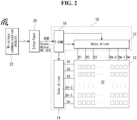
FIG. 2 is a block diagram showing in detail a display panel, a display panel driver, and a timing controller; and -
FIGS. 3 to 13 are views showing various embodiments of a PCB in a wireless display sink device. - Hereinafter, exemplary embodiments of this document will be described in detail with reference to the attached drawings. Throughout the specification, like reference numerals denote substantially like components. Hereinafter, the detailed description of related known functions or configurations that may unnecessarily obscure the subject matter of the present invention in describing the present invention will be omitted.
- In the following description, a source device is a device that transmits video/audio data streams. Examples of the source device may include a mobile device such as a smartphone or a laptop, a navigation system, a set-top box, a DVD player, a Blu-ray player, and a computer.
- A wireless display sink device comprises a display panel, a display panel driver, a timing controller that controls the display panel driver, and a wireless communication module. The wireless display sink device establishes a wireless communication link with a source device through a wireless communication module without its own wireless communication device such as an AP or dongle.
- The wireless display sink device is connected to the display panel driver. A display device connected to the display panel driver may be implemented as a flat panel display device, such as a liquid crystal display (LCD), a field emission display (FED), a plasma display panel (PDP), an organic light emitting display (OLED), or an electrophoresis display (EPD).
- Referring to
FIGS. 1 and2 , the source device comprises anencoder 2 and a wireless communication module 4. - The wireless display sink device comprises a
display panel driver 18 and a PCB (Printed Circuit Board) connected to the wireless communication module. The PCB comprises awireless communication module 26, adecoder 22, an audio DAC (Digital Analog Converter) 24, aninterface 20, and a timing controller (T-CON) 16. - The source device transmits encoded video and audio data streams to the wireless display sink device. The
encoder 2 encodes video and audio data by a predetermined algorithm. For example, theencoder 2 may encode video data in MPEG4 or H.264 format and encode audio data in LPCM44.1, LPCM16-48, AAC, AC-3, AAA, AMR, WMA, MPEG-2 Audio, or MPEG-4 Audio format. The encoded video and audio data streams are transmitted to the wireless display sink device through the wireless communication module 4. - The wireless communication module 4 of the source device and the
wireless communication module 26 of the wireless display sink device may transmit and receive data according to a wireless data communication standard or cellular communication standard. The wireless data communication standard comprises IEEE 802.16 (for wireless metropolitan area networks) such as WiMax and Wibro, IEE 802.15 (for wireless personal area networks) such as Bluetooth, Zigbee, UWB, and Li-FI, and IEEE 802.11 (for wireless local area networks) such as Wi-Fi and WiGig. The cellular communication standard comprises 4G standards such as fD-LTE and TD-LTE, 3G standards such as WCDMA, GSM, HDSA, HDSA+, and CDMA2000, and 2G standards such as CDMA and GSM. - The
decoder 22 decodes data streams received from thewireless communication module 26 to restore audio data and video data and separate them. Thedecoder 22 implements a restoration algorithm corresponding to the algorithm of theencoder 2 equivalent to that of theencoder 2 to decode data received through thewireless communication module 26 and restore video data and audio data to their state before encoding. - The
audio DAC 24 converts audio data into an analog voltage and outputs it to an audio player, i.e., speaker. Theinterface 20 delivers the video data input from thedecoder 22 to thetiming controller 16. - The
display panel driver 18 writes video data of an input image to the pixels of adisplay panel 10. The display panel comprises a pixel array that displays video data of an input image. The pixel array comprises a plurality of data lines D1 to Dm (m is a positive integer), a plurality of scan lines G1 to Gm (n is a positive integer) crossing the data lines D1 to Dm, and pixels arranged in a matrix form. Color filters for color representation may be formed on thedisplay panel 10. - The
display panel driver 18 comprises adata driver 12 and ascan driver 14 that are connected to thedisplay panel 10. Thedata driver 12 comprises a plurality of source drive ICs (Integrated Circuits). The SICs ofFIG. 3 are source drive ICs. Thedata driver 12 converts video data input from the timing controller into a gamma compensation voltage to generate a data voltage and supply the data voltage to the data lines D1 to Dm. Thescan driver 14 sequentially supplies a scan pulse (or gate pulse) synchronized with the data voltage to the scan lines G1 to Gn and selects lines of thedisplay panel 10 to which data is written. - The
timing controller 16 transmits video data of an input image to thedata driver 12 by a signal defined according to a mini LVDS (Low-Voltage Differential Signaling) interface protocol or EPI (Embedded Panel Interface) interface protocol. The interface technologies proposed inKorean Patent Application No. 10-2008-0127458 2008-12-15 U.S. Patent Application No. 12/543,996 2009- 08-19 ),Korean Patent Application No. 10-2008-0127456 2008-12-15 U.S. Patent Application 12/461,6522009-08-19 Korean Patent Application No. 10-2008-0132466 2008-12-23 U.S. Patent Application No. 12/537,341 2009-08-07 timing controller 16 controls the operation timing of thedisplay panel driver 18 based on timing signals received together with video data. The timing signals comprise a vertical synchronization signal Vsync, a horizontal synchronization signal Hsync, a clock signal CLK, a data enable signal DE, and a main clock MCLK. -
FIGS. 3 to 13 are views showing various examples where the components ofFIG. 1 are mounted on the PCB of the wireless display sink device. - Referring to
FIG. 3 , PCB1 is connected to thedisplay panel driver 18 through a flexible circuit such as an FFC (Flexible Flat Circuit) or an FPC (Flexible Printed Circuit). - The
decoder 22, theaudio DAC 24, theinterface 20, thetiming controller 16, etc are mounted on PCB1. Thewireless communication module 26 is connected to PCB1. A cable connected to thewireless communication module 26 may be connected to aconnector 21 mounted on PCB1. - Referring to
FIG. 4 , not being part of the present invention, thedecoder 22 may output restored video data in a TMDS (Transition Minimized Differential Signaling) format defined according to the HDMI (High-Definition Multimedia Interface) standard. Theinterface 20 converts video data, which is received in a TMDS signal for HDMI, into an LVDS signal format, a display data transmission format, and transmits it to thetiming controller 16. Thetiming controller 16 converts the video data of the LVDS signal received from theinterface 20 into a mini-LVDS interface signal or EPI interface signal and transmits it to thedata driver 12. - Referring to
FIG. 5 , not being part of the invention, thedecoder 22 may output restored video data and audio data in HDMI signal format. Theinterface 20 separates video data from an HDMI signal, and converts the video data into a DP (DisplayPort) signal complying with a display data transmission standard. Thetiming controller 16 converts video data of a DP signal received from theinterface 20 into a mini-LVDS interface or EPI interface signal and transmits it to thedata driver 12. - Referring to
FIG. 6 , thedecoder 22 outputs restored video data in HDMI signal format. Thetiming controller 16 converts the video data of the HDMI signal received from theinterface 20 into a mini-LVDS interface signal or EPI interface signal and transmits it to thedata driver 12. The HDMI signal contains audio data and video data. The timing controller separates audio data and video data, and transmits only the video data to thedata driver 12. In this exemplary embodiment, a TMD signal is transmitted directly to thetiming controller 16, so theinterface 20 for switching interfaces is omitted, thereby reducing switching loss and circuit costs. - Referring to
FIG. 7 , thewireless communication module 26 is connected to PCB1 through acard slot 27. In this case, thewireless communication module 26 is in the form of a card and detachably connected to a slot mounted on PCB1. - A display device requires a power supply part that generates power and supplies it to the pixels of the
display panel 10. A liquid crystal display LCD may comprise a backlight unit for illuminating thedisplay panel 10 and a light source driver for turning on the light sources of the backlight unit. PCB1 is designed as shown inFIG. 8 and the power supply part and the light source driver are mounted on PCB1. - Referring to
FIG. 8 , apower supply part 32 and alight source driver 34 are further mounted on PCB1. Thepower supply part 32 generates power and applies it to the pixels of thedisplay panel 10, for instance, a common voltage Vcom and gamma compensation voltage for a liquid crystal display LCD, a pixel driving voltage ELVDD for an organic light emitting display OLED, a scan pulse voltage, etc. Thelight source driver 34 generates a light source driving voltage required to turn on backlight sources. The backlight sources may be LEDs (Light Emitting Diodes). - PCB1 comprises video/audio lines through which video data and audio data are transmitted in high-frequency signals between the
wireless communication module 26 and thedecoder 122. The output voltages of thepower supply part 32 andlight source driver 34 are much higher than those of other circuits. Due to this, the high-frequency signals transmitted at low voltages through the video/audio lines may be affected and distorted by thepower supply part 32 and thelight source driver 34. To avoid this, PCB1 further comprises aslot 30 formed around either or both of thepower supply part 32 and thelight source driver 34 and anotherslot 36 formed between either or both of thepower supply part 32 and thelight source driver 34 and the video/audio lines. - The
decoder 22 may incorporate a scaler to adjust the resolution of an input image in accordance with the resolution of thedisplay panel 10. The scaler of thedecoder 122 may convert video data input throughexternal input terminals 38 mounted on PCB1 from the original resolution to the resolution of thedisplay panel 10. A standard cable such as HDMI, DVI (Digital Visual Interface), or D-SUB is connected to the external input terminals to receive video data via the cable. - In the exemplary embodiment shown in
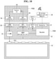
FIG. 8 , no scaler board is required because a scaler is embedded in the decoder.FIGS. 9 and10 show examples where a scaler board PCB2 is connected to PCB1. - Referring to
FIG. 9 , the scaler board PCB2 is connected to PCB1 viaHDMI connectors HDMI connectors LVDS connectors LVDS connectors - Video data in HDMI signal format output from the
decoder 22 is transmitted to ascaler IC 46 via theHDMI connectors scaler IC 46 converts video data received in an HDMI signal from the original resolution to the resolution of thedisplay panel 10, and outputs the video data in an LVDS signal. The video data output from thescaler IC 46 is transmitted to thetiming controller 16 via theLVDS connectors - Referring to
FIG. 10 , the scaler board PCB2 is connected to PCB1 viaDVI connectors DVI connectors LVDS connectors LVDS connectors - The source device may encrypt video data by HDCP (High-Bandwidth Digital Content Protection) encryption to transmit it by the wireless display sink device. In this case, the wireless display sink device must use an HDCP decryption unit to restore the original video data. The
HDCP decryption unit 52 may be embedded in thedecoder 22 or connected to the output terminal of thedecoder 22. TheHDCP decryption unit 52 may be likewise connected to thedecoder 22 in the foregoing embodiments. - The
HDCP decryption unit 52 outputs restored video data in a DVI signal or HDMI signal. The DVI signal is transmitted to thescaler IC 56 via theDVI connectors scaler IC 56 converts video data received in a DVI signal from the original resolution to the resolution of thedisplay panel 10, and outputs the video data in an LVDS signal. The video data output from thescaler IC 56 is transmitted to thetiming controller 16 via theLVDS connectors - Referring to
FIG. 11 , thetiming controller 16 receives signals through 2-port input terminals. The first input port of thetiming controller 16 is connected to the output terminal of thedecoder 22 orHCDP decryption unit 52 to receive output signals from thedecoder 22, and the second input port may be connected to an external connector 6 to receive external input signals. The external connector 6 may be connected to an external video source via a cable to transmit video data signals received from the external video source directly to thetiming controller 16. - As shown in
FIG. 12 , the screen of thedisplay panel 10 may be implemented as a touch screen TSP comprising touch sensors. A touch sensing driver detects touch input by sensing a signal variation in the touch sensors. - Referring to
FIG. 12 , the touch sensing driver may comprise an ROIC (Readout Integrated Circuit) 78 that applies a drive signal to the touch sensors, detects a touch sensor signal variation, and converts it into a digital value and an MCU (Micro Controller Unit) 76 that compares the digital value with a predetermined threshold value and estimates the presence or absence of touch input and the coordinates of a touch input position. The touch sensing driver may be mounted on a touch signal processing board PCB3. The touch signal processing board PCB3 may be connected to the lines of the touch screen via a flexible circuit or cable. - The touch signal processing board PCB3 may be connected to PCB1 through USB (Universal Serial Bus)
connectors MCU 76 is transmitted to PCB1 through the USB connectors, converted into a wireless signal through a wireless communication module, and transmitted to the source device. The touch report contains coordinate information of each touch input. The source device runs an application program associated with the touch input coordinates. - The touch sensors and touch sensing driver of
FIG. 12 may further involve gesture sensing and recognition functions. In this case, gesture input coordinate information, along with the touch input coordinates, may be transmitted into a wireless signal and transmitted to the source device. - Referring to
FIG. 13 , thedecoder 22 may output video data separated from an HDMI signal in a TMDS signal and transmit the TMDS signal directly to thetiming controller 16. - The configurations of the wireless display sink devices shown in
FIGS. 3 to 13 can be used in combination. As shown inFIG. 8 , the method of forming a power supply part, a light source driver, and a slot may be applied to the PCBs disclosed in other exemplary embodiments. - As described above, a wireless display sink device can wirelessly share contents with a source device by connecting a wireless communication module to a PCB with a timing controller mounted on it to control a display panel driver and enable N-screen service by screen mirroring.
- Although embodiments have been described with reference to a number of illustrative embodiments thereof, it should be understood that numerous other modifications and embodiments can be devised by those skilled in the art that will fall within the scope of the principles of this disclosure. More particularly, various variations and modifications are possible in the component parts and/or arrangements of the subject combination arrangement within the scope of the disclosure, the drawings and the appended claims. In addition to variations and modifications in the component parts and/or arrangements, alternative uses will also be apparent to those skilled in the art.
Claims (4)
- A wireless display sink device comprising a display panel driver (18), a PCB, Printed Circuit Board, a detachable wireless communication module (26) connected to the PCB through a card slot (27), and a backlight unit that is configured to illuminate a display panel, the PCB comprising:a decoder (22) that is configured to decode audio/video data received from the detachable wireless communication module and is configured to separate audio data and video data;an audio DAC (24), Digital Analog Converter, that is configured to convert the audio data into an analog signal;a timing controller (16) that is configured to transmit the video data to the display panel driver and is configured to control the operation timing of the display panel driver;a power supply part (32) that is configured to generate power and is configured to supply the power to pixels of the display panel;a light source driver (34) that is configured to generate a light source driving voltage to turn on the light sources of the backlight unit;video/audio lines that are configured to transmit video data and audio data in high-frequency signals between the detachable wireless communication module and the decoder;a first shield slot (30) around at least one of the power supply part (32) and the light source driver (34); anda second shield slot (36) between at least one of the power supply part (32) and the light source driver (34) and the video/audio lines,
wherein the timing controller is configured to receive an HDMI signal or TMDS, Transition Minimized Differential Signaling, signal output directly from the decoder,wherein the wireless display sink device further comprises a decryption unit (52) connected to an output terminal of the decoder that is configured to restore a signal encrypted by HDPC, High-bandwidth Digital Content Protection, format and received from the decoder,wherein the PCB further comprises a connector (60) that is configured to receive an external input video signal via a cable, and the timing controller is configured to receive an output video signal from the decoder through a first input port and to receive the external input video signal through a second input port. - The wireless display sink device of claim 1, wherein the PCB further comprises:an external input terminal for receiving an HDMI signal;an external input terminal for receiving a DVI, Digital Visual Interface, signal; andan external input terminal for receiving a D-SUB signal.
- The wireless display sink device of claim 1, further comprising a scaler board connected to the PCB,the scaler board having a scaler IC, Integrated Circuit, mounted thereon,wherein the scaler IC is configured to convert an HDMI signal received from the decoder into an LVDS signal or DVI signal and is configured to transmit the signal to the timing controller.
- The wireless display sink device of claim 1, further comprising:a touch screen formed on the display panel; anda sensing circuit that is configured to sense touch input or gesture input by analyzing a signal on the touch screen,wherein the wireless display sink is configured to transmit coordinate information output from sensing circuit to the PCB over a USB, Universal Serial Bus, path, to convert it into a wireless signal through the detachable wireless communication module, and to transmit it to an external source device.
Applications Claiming Priority (1)
| Application Number | Priority Date | Filing Date | Title |
|---|---|---|---|
| KR1020130166171A KR102143222B1 (en) | 2013-12-27 | 2013-12-27 | Wireless display sink device |
Publications (2)
| Publication Number | Publication Date |
|---|---|
| EP2889874A1 EP2889874A1 (en) | 2015-07-01 |
| EP2889874B1 true EP2889874B1 (en) | 2024-06-05 |
Family
ID=52103062
Family Applications (1)
| Application Number | Title | Priority Date | Filing Date |
|---|---|---|---|
| EP14197886.6A Active EP2889874B1 (en) | 2013-12-27 | 2014-12-15 | Wireless display sink device |
Country Status (4)
| Country | Link |
|---|---|
| US (1) | US9473731B2 (en) |
| EP (1) | EP2889874B1 (en) |
| KR (1) | KR102143222B1 (en) |
| CN (1) | CN104754380B (en) |
Families Citing this family (17)
| Publication number | Priority date | Publication date | Assignee | Title |
|---|---|---|---|---|
| US10277275B2 (en) | 2015-09-08 | 2019-04-30 | Google Llc | Audio media streaming device |
| US9736531B2 (en) * | 2015-09-08 | 2017-08-15 | Google Inc. | Video media streaming device |
| US10084498B2 (en) * | 2015-09-16 | 2018-09-25 | Gm Global Technology Operations, Llc. | Configurable communications module with replaceable network access device |
| KR102577493B1 (en) * | 2016-07-29 | 2023-09-11 | 엘지디스플레이 주식회사 | Organic light emitting device and its driving method |
| JP6730144B2 (en) * | 2016-09-09 | 2020-07-29 | 株式会社シマノ | Bicycle component and its communication part |
| KR102444156B1 (en) * | 2017-09-22 | 2022-09-16 | 삼성디스플레이 주식회사 | Display device and mehthod for driving the same |
| CN109166538B (en) * | 2018-11-22 | 2023-10-20 | 合肥惠科金扬科技有限公司 | Control circuit of display panel and display device |
| CN109521360A (en) * | 2018-12-28 | 2019-03-26 | 广东电网有限责任公司 | Relay contact signal detection equipment and system |
| KR102697989B1 (en) | 2019-04-15 | 2024-08-22 | 삼성전자주식회사 | Display apparatus and the control method thereof |
| US10785386B1 (en) * | 2019-12-17 | 2020-09-22 | Realtek Semiconductor Corp. | DP to HDMI converter and associated signal conversion method |
| KR102666715B1 (en) * | 2019-12-26 | 2024-05-17 | 엘지디스플레이 주식회사 | Display device |
| CN111083409A (en) * | 2019-12-27 | 2020-04-28 | 苏州斯拓锐网络科技有限公司 | Novel AI picture passes module |
| KR102463351B1 (en) | 2021-09-15 | 2022-11-04 | 엘지전자 주식회사 | Display device and operating method thereof |
| CN114363692A (en) * | 2021-12-30 | 2022-04-15 | Tcl华星光电技术有限公司 | Chip system applied to video equipment, video equipment and display system |
| CN114488833B (en) * | 2022-01-19 | 2025-04-22 | 北京小米移动软件有限公司 | Circuit board of household appliances and household appliances |
| US12211461B2 (en) | 2022-09-19 | 2025-01-28 | Samsung Electronics Co., Ltd. | Display apparatus and method of controlling the same |
| CN119274508A (en) * | 2024-11-20 | 2025-01-07 | 拓旷(上海)光电科技有限公司 | Driving method and system based on display panel |
Citations (3)
| Publication number | Priority date | Publication date | Assignee | Title |
|---|---|---|---|---|
| US5699231A (en) * | 1995-11-24 | 1997-12-16 | Xerox Corporation | Method of packaging high voltage components with low voltage components in a small space |
| EP1289341A2 (en) * | 2001-08-16 | 2003-03-05 | Hella KG Hueck & Co. | Automotive lighting device with associated circuit and printed circuit board |
| US20080084166A1 (en) * | 2005-03-01 | 2008-04-10 | Jean Co., Ltd | Layout configuration of flat display device |
Family Cites Families (9)
| Publication number | Priority date | Publication date | Assignee | Title |
|---|---|---|---|---|
| US20060209892A1 (en) * | 2005-03-15 | 2006-09-21 | Radiospire Networks, Inc. | System, method and apparatus for wirelessly providing a display data channel between a generalized content source and a generalized content sink |
| US7499462B2 (en) * | 2005-03-15 | 2009-03-03 | Radiospire Networks, Inc. | System, method and apparatus for wireless delivery of content from a generalized content source to a generalized content sink |
| US7701451B1 (en) * | 2005-07-29 | 2010-04-20 | Pixelworks, Inc. | Boost look up table compression system and method |
| KR20120015931A (en) * | 2010-08-13 | 2012-02-22 | 삼성전자주식회사 | Portable electronic device and its display mirroring method |
| US9244500B2 (en) * | 2011-05-23 | 2016-01-26 | Intel Corporation | System integration supporting completely wireless peripheral applications |
| TW201250530A (en) * | 2011-06-07 | 2012-12-16 | Hannstar Display Corp | Integrated touch panel structure and manufacturing method thereof |
| US9286854B2 (en) | 2011-10-31 | 2016-03-15 | Roku, Inc. | Multi-interface streaming media system |
| US9594536B2 (en) | 2011-12-29 | 2017-03-14 | Ati Technologies Ulc | Method and apparatus for electronic device communication |
| US9167296B2 (en) * | 2012-02-28 | 2015-10-20 | Qualcomm Incorporated | Customized playback at sink device in wireless display system |
-
2013
- 2013-12-27 KR KR1020130166171A patent/KR102143222B1/en active Active
-
2014
- 2014-10-07 US US14/508,350 patent/US9473731B2/en active Active
- 2014-10-30 CN CN201410601651.6A patent/CN104754380B/en active Active
- 2014-12-15 EP EP14197886.6A patent/EP2889874B1/en active Active
Patent Citations (3)
| Publication number | Priority date | Publication date | Assignee | Title |
|---|---|---|---|---|
| US5699231A (en) * | 1995-11-24 | 1997-12-16 | Xerox Corporation | Method of packaging high voltage components with low voltage components in a small space |
| EP1289341A2 (en) * | 2001-08-16 | 2003-03-05 | Hella KG Hueck & Co. | Automotive lighting device with associated circuit and printed circuit board |
| US20080084166A1 (en) * | 2005-03-01 | 2008-04-10 | Jean Co., Ltd | Layout configuration of flat display device |
Also Published As
| Publication number | Publication date |
|---|---|
| EP2889874A1 (en) | 2015-07-01 |
| US9473731B2 (en) | 2016-10-18 |
| KR102143222B1 (en) | 2020-08-11 |
| CN104754380A (en) | 2015-07-01 |
| US20150189218A1 (en) | 2015-07-02 |
| KR20150077598A (en) | 2015-07-08 |
| CN104754380B (en) | 2018-04-06 |
Similar Documents
| Publication | Publication Date | Title |
|---|---|---|
| US9473731B2 (en) | Wireless display sink device | |
| US12254804B2 (en) | Display apparatus and driving power control method thereof | |
| KR102112089B1 (en) | Display device and driving method thereof | |
| KR101615813B1 (en) | Touch sensing apparatus for time division driving type | |
| KR102057502B1 (en) | Display Drive IC and Image Display System | |
| KR102009440B1 (en) | Apparatus and method of controlling data interface | |
| CN104835470B (en) | Display base plate driving device and driving method, display equipment | |
| KR102666273B1 (en) | Display device having touch sensor using the same and driving method thereof | |
| KR20160093181A (en) | Command inputting method and display system | |
| EP1942486A2 (en) | Display apparatus for displaying video input through various connectors | |
| KR102270600B1 (en) | Display device | |
| TWI635472B (en) | Systems, system components and methods for operating the same | |
| KR102212208B1 (en) | Data Driving Circuit Device for Display Device and Display Device having the same | |
| US9299315B2 (en) | Source driving circuit and data transmission method thereof | |
| CN104575351A (en) | Signal conversion system, displayer and signal conversion method | |
| US9478190B2 (en) | Video card and computer | |
| US20160247473A1 (en) | Transmission device, reception device, transmission/reception system, and image display system | |
| US12619491B2 (en) | Display processing device, a data transmission method, and an image data inspection method | |
| CN105336301A (en) | Liquid crystal display device | |
| CN205068363U (en) | Conversion IC who shows signal | |
| US20160239140A1 (en) | Touch screen display and bidirectional data transmission method | |
| JP2014147041A (en) | Electronic apparatus and display device | |
| US20240320811A1 (en) | Display drive device and image data inspection method | |
| CN209748696U (en) | Miniature display driving circuit system | |
| KR20260011358A (en) | Display apparatus |
Legal Events
| Date | Code | Title | Description |
|---|---|---|---|
| PUAI | Public reference made under article 153(3) epc to a published international application that has entered the european phase |
Free format text: ORIGINAL CODE: 0009012 |
|
| 17P | Request for examination filed |
Effective date: 20141215 |
|
| AK | Designated contracting states |
Kind code of ref document: A1 Designated state(s): AL AT BE BG CH CY CZ DE DK EE ES FI FR GB GR HR HU IE IS IT LI LT LU LV MC MK MT NL NO PL PT RO RS SE SI SK SM TR |
|
| AX | Request for extension of the european patent |
Extension state: BA ME |
|
| R17P | Request for examination filed (corrected) |
Effective date: 20151216 |
|
| RBV | Designated contracting states (corrected) |
Designated state(s): AL AT BE BG CH CY CZ DE DK EE ES FI FR GB GR HR HU IE IS IT LI LT LU LV MC MK MT NL NO PL PT RO RS SE SI SK SM TR |
|
| STAA | Information on the status of an ep patent application or granted ep patent |
Free format text: STATUS: EXAMINATION IS IN PROGRESS |
|
| 17Q | First examination report despatched |
Effective date: 20181009 |
|
| GRAP | Despatch of communication of intention to grant a patent |
Free format text: ORIGINAL CODE: EPIDOSNIGR1 |
|
| STAA | Information on the status of an ep patent application or granted ep patent |
Free format text: STATUS: GRANT OF PATENT IS INTENDED |
|
| INTG | Intention to grant announced |
Effective date: 20240125 |
|
| RIC1 | Information provided on ipc code assigned before grant |
Ipc: H04N 21/41 20110101ALI20240112BHEP Ipc: H04N 21/4363 20110101ALI20240112BHEP Ipc: G09G 5/00 20060101AFI20240112BHEP |
|
| GRAS | Grant fee paid |
Free format text: ORIGINAL CODE: EPIDOSNIGR3 |
|
| GRAA | (expected) grant |
Free format text: ORIGINAL CODE: 0009210 |
|
| STAA | Information on the status of an ep patent application or granted ep patent |
Free format text: STATUS: THE PATENT HAS BEEN GRANTED |
|
| AK | Designated contracting states |
Kind code of ref document: B1 Designated state(s): AL AT BE BG CH CY CZ DE DK EE ES FI FR GB GR HR HU IE IS IT LI LT LU LV MC MK MT NL NO PL PT RO RS SE SI SK SM TR |
|
| REG | Reference to a national code |
Ref country code: GB Ref legal event code: FG4D |
|
| REG | Reference to a national code |
Ref country code: CH Ref legal event code: EP |
|
| REG | Reference to a national code |
Ref country code: DE Ref legal event code: R096 Ref document number: 602014090292 Country of ref document: DE |
|
| REG | Reference to a national code |
Ref country code: IE Ref legal event code: FG4D |
|
| REG | Reference to a national code |
Ref country code: LT Ref legal event code: MG9D |
|
| PG25 | Lapsed in a contracting state [announced via postgrant information from national office to epo] |
Ref country code: BG Free format text: LAPSE BECAUSE OF FAILURE TO SUBMIT A TRANSLATION OF THE DESCRIPTION OR TO PAY THE FEE WITHIN THE PRESCRIBED TIME-LIMIT Effective date: 20240605 |
|
| REG | Reference to a national code |
Ref country code: NL Ref legal event code: MP Effective date: 20240605 |
|
| PG25 | Lapsed in a contracting state [announced via postgrant information from national office to epo] |
Ref country code: HR Free format text: LAPSE BECAUSE OF FAILURE TO SUBMIT A TRANSLATION OF THE DESCRIPTION OR TO PAY THE FEE WITHIN THE PRESCRIBED TIME-LIMIT Effective date: 20240605 Ref country code: FI Free format text: LAPSE BECAUSE OF FAILURE TO SUBMIT A TRANSLATION OF THE DESCRIPTION OR TO PAY THE FEE WITHIN THE PRESCRIBED TIME-LIMIT Effective date: 20240605 |
|
| PG25 | Lapsed in a contracting state [announced via postgrant information from national office to epo] |
Ref country code: GR Free format text: LAPSE BECAUSE OF FAILURE TO SUBMIT A TRANSLATION OF THE DESCRIPTION OR TO PAY THE FEE WITHIN THE PRESCRIBED TIME-LIMIT Effective date: 20240906 |
|
| PG25 | Lapsed in a contracting state [announced via postgrant information from national office to epo] |
Ref country code: ES Free format text: LAPSE BECAUSE OF FAILURE TO SUBMIT A TRANSLATION OF THE DESCRIPTION OR TO PAY THE FEE WITHIN THE PRESCRIBED TIME-LIMIT Effective date: 20240605 |
|
| PG25 | Lapsed in a contracting state [announced via postgrant information from national office to epo] |
Ref country code: LV Free format text: LAPSE BECAUSE OF FAILURE TO SUBMIT A TRANSLATION OF THE DESCRIPTION OR TO PAY THE FEE WITHIN THE PRESCRIBED TIME-LIMIT Effective date: 20240605 |
|
| PG25 | Lapsed in a contracting state [announced via postgrant information from national office to epo] |
Ref country code: NO Free format text: LAPSE BECAUSE OF FAILURE TO SUBMIT A TRANSLATION OF THE DESCRIPTION OR TO PAY THE FEE WITHIN THE PRESCRIBED TIME-LIMIT Effective date: 20240905 Ref country code: LV Free format text: LAPSE BECAUSE OF FAILURE TO SUBMIT A TRANSLATION OF THE DESCRIPTION OR TO PAY THE FEE WITHIN THE PRESCRIBED TIME-LIMIT Effective date: 20240605 Ref country code: HR Free format text: LAPSE BECAUSE OF FAILURE TO SUBMIT A TRANSLATION OF THE DESCRIPTION OR TO PAY THE FEE WITHIN THE PRESCRIBED TIME-LIMIT Effective date: 20240605 Ref country code: GR Free format text: LAPSE BECAUSE OF FAILURE TO SUBMIT A TRANSLATION OF THE DESCRIPTION OR TO PAY THE FEE WITHIN THE PRESCRIBED TIME-LIMIT Effective date: 20240906 Ref country code: FI Free format text: LAPSE BECAUSE OF FAILURE TO SUBMIT A TRANSLATION OF THE DESCRIPTION OR TO PAY THE FEE WITHIN THE PRESCRIBED TIME-LIMIT Effective date: 20240605 Ref country code: ES Free format text: LAPSE BECAUSE OF FAILURE TO SUBMIT A TRANSLATION OF THE DESCRIPTION OR TO PAY THE FEE WITHIN THE PRESCRIBED TIME-LIMIT Effective date: 20240605 Ref country code: BG Free format text: LAPSE BECAUSE OF FAILURE TO SUBMIT A TRANSLATION OF THE DESCRIPTION OR TO PAY THE FEE WITHIN THE PRESCRIBED TIME-LIMIT Effective date: 20240605 Ref country code: RS Free format text: LAPSE BECAUSE OF FAILURE TO SUBMIT A TRANSLATION OF THE DESCRIPTION OR TO PAY THE FEE WITHIN THE PRESCRIBED TIME-LIMIT Effective date: 20240905 |
|
| PG25 | Lapsed in a contracting state [announced via postgrant information from national office to epo] |
Ref country code: NL Free format text: LAPSE BECAUSE OF FAILURE TO SUBMIT A TRANSLATION OF THE DESCRIPTION OR TO PAY THE FEE WITHIN THE PRESCRIBED TIME-LIMIT Effective date: 20240605 |
|
| REG | Reference to a national code |
Ref country code: AT Ref legal event code: MK05 Ref document number: 1693045 Country of ref document: AT Kind code of ref document: T Effective date: 20240605 |
|
| PG25 | Lapsed in a contracting state [announced via postgrant information from national office to epo] |
Ref country code: NL Free format text: LAPSE BECAUSE OF FAILURE TO SUBMIT A TRANSLATION OF THE DESCRIPTION OR TO PAY THE FEE WITHIN THE PRESCRIBED TIME-LIMIT Effective date: 20240605 |
|
| PG25 | Lapsed in a contracting state [announced via postgrant information from national office to epo] |
Ref country code: PT Free format text: LAPSE BECAUSE OF FAILURE TO SUBMIT A TRANSLATION OF THE DESCRIPTION OR TO PAY THE FEE WITHIN THE PRESCRIBED TIME-LIMIT Effective date: 20241007 |
|
| PG25 | Lapsed in a contracting state [announced via postgrant information from national office to epo] |
Ref country code: PT Free format text: LAPSE BECAUSE OF FAILURE TO SUBMIT A TRANSLATION OF THE DESCRIPTION OR TO PAY THE FEE WITHIN THE PRESCRIBED TIME-LIMIT Effective date: 20241007 |
|
| PG25 | Lapsed in a contracting state [announced via postgrant information from national office to epo] |
Ref country code: PL Free format text: LAPSE BECAUSE OF FAILURE TO SUBMIT A TRANSLATION OF THE DESCRIPTION OR TO PAY THE FEE WITHIN THE PRESCRIBED TIME-LIMIT Effective date: 20240605 |
|
| PG25 | Lapsed in a contracting state [announced via postgrant information from national office to epo] |
Ref country code: EE Free format text: LAPSE BECAUSE OF FAILURE TO SUBMIT A TRANSLATION OF THE DESCRIPTION OR TO PAY THE FEE WITHIN THE PRESCRIBED TIME-LIMIT Effective date: 20240605 |
|
| PG25 | Lapsed in a contracting state [announced via postgrant information from national office to epo] |
Ref country code: AT Free format text: LAPSE BECAUSE OF FAILURE TO SUBMIT A TRANSLATION OF THE DESCRIPTION OR TO PAY THE FEE WITHIN THE PRESCRIBED TIME-LIMIT Effective date: 20240605 Ref country code: IS Free format text: LAPSE BECAUSE OF FAILURE TO SUBMIT A TRANSLATION OF THE DESCRIPTION OR TO PAY THE FEE WITHIN THE PRESCRIBED TIME-LIMIT Effective date: 20241005 |
|
| PG25 | Lapsed in a contracting state [announced via postgrant information from national office to epo] |
Ref country code: CZ Free format text: LAPSE BECAUSE OF FAILURE TO SUBMIT A TRANSLATION OF THE DESCRIPTION OR TO PAY THE FEE WITHIN THE PRESCRIBED TIME-LIMIT Effective date: 20240605 |
|
| PG25 | Lapsed in a contracting state [announced via postgrant information from national office to epo] |
Ref country code: RO Free format text: LAPSE BECAUSE OF FAILURE TO SUBMIT A TRANSLATION OF THE DESCRIPTION OR TO PAY THE FEE WITHIN THE PRESCRIBED TIME-LIMIT Effective date: 20240605 Ref country code: SK Free format text: LAPSE BECAUSE OF FAILURE TO SUBMIT A TRANSLATION OF THE DESCRIPTION OR TO PAY THE FEE WITHIN THE PRESCRIBED TIME-LIMIT Effective date: 20240605 |
|
| PG25 | Lapsed in a contracting state [announced via postgrant information from national office to epo] |
Ref country code: SM Free format text: LAPSE BECAUSE OF FAILURE TO SUBMIT A TRANSLATION OF THE DESCRIPTION OR TO PAY THE FEE WITHIN THE PRESCRIBED TIME-LIMIT Effective date: 20240605 |
|
| PG25 | Lapsed in a contracting state [announced via postgrant information from national office to epo] |
Ref country code: SM Free format text: LAPSE BECAUSE OF FAILURE TO SUBMIT A TRANSLATION OF THE DESCRIPTION OR TO PAY THE FEE WITHIN THE PRESCRIBED TIME-LIMIT Effective date: 20240605 Ref country code: SK Free format text: LAPSE BECAUSE OF FAILURE TO SUBMIT A TRANSLATION OF THE DESCRIPTION OR TO PAY THE FEE WITHIN THE PRESCRIBED TIME-LIMIT Effective date: 20240605 Ref country code: RO Free format text: LAPSE BECAUSE OF FAILURE TO SUBMIT A TRANSLATION OF THE DESCRIPTION OR TO PAY THE FEE WITHIN THE PRESCRIBED TIME-LIMIT Effective date: 20240605 Ref country code: PL Free format text: LAPSE BECAUSE OF FAILURE TO SUBMIT A TRANSLATION OF THE DESCRIPTION OR TO PAY THE FEE WITHIN THE PRESCRIBED TIME-LIMIT Effective date: 20240605 Ref country code: IS Free format text: LAPSE BECAUSE OF FAILURE TO SUBMIT A TRANSLATION OF THE DESCRIPTION OR TO PAY THE FEE WITHIN THE PRESCRIBED TIME-LIMIT Effective date: 20241005 Ref country code: EE Free format text: LAPSE BECAUSE OF FAILURE TO SUBMIT A TRANSLATION OF THE DESCRIPTION OR TO PAY THE FEE WITHIN THE PRESCRIBED TIME-LIMIT Effective date: 20240605 Ref country code: CZ Free format text: LAPSE BECAUSE OF FAILURE TO SUBMIT A TRANSLATION OF THE DESCRIPTION OR TO PAY THE FEE WITHIN THE PRESCRIBED TIME-LIMIT Effective date: 20240605 Ref country code: AT Free format text: LAPSE BECAUSE OF FAILURE TO SUBMIT A TRANSLATION OF THE DESCRIPTION OR TO PAY THE FEE WITHIN THE PRESCRIBED TIME-LIMIT Effective date: 20240605 |
|
| PG25 | Lapsed in a contracting state [announced via postgrant information from national office to epo] |
Ref country code: IT Free format text: LAPSE BECAUSE OF FAILURE TO SUBMIT A TRANSLATION OF THE DESCRIPTION OR TO PAY THE FEE WITHIN THE PRESCRIBED TIME-LIMIT Effective date: 20240605 |
|
| REG | Reference to a national code |
Ref country code: DE Ref legal event code: R097 Ref document number: 602014090292 Country of ref document: DE |
|
| PLBE | No opposition filed within time limit |
Free format text: ORIGINAL CODE: 0009261 |
|
| STAA | Information on the status of an ep patent application or granted ep patent |
Free format text: STATUS: NO OPPOSITION FILED WITHIN TIME LIMIT |
|
| PG25 | Lapsed in a contracting state [announced via postgrant information from national office to epo] |
Ref country code: DK Free format text: LAPSE BECAUSE OF FAILURE TO SUBMIT A TRANSLATION OF THE DESCRIPTION OR TO PAY THE FEE WITHIN THE PRESCRIBED TIME-LIMIT Effective date: 20240605 |
|
| 26N | No opposition filed |
Effective date: 20250306 |
|
| PG25 | Lapsed in a contracting state [announced via postgrant information from national office to epo] |
Ref country code: MC Free format text: LAPSE BECAUSE OF FAILURE TO SUBMIT A TRANSLATION OF THE DESCRIPTION OR TO PAY THE FEE WITHIN THE PRESCRIBED TIME-LIMIT Effective date: 20240605 |
|
| REG | Reference to a national code |
Ref country code: CH Ref legal event code: PL |
|
| PG25 | Lapsed in a contracting state [announced via postgrant information from national office to epo] |
Ref country code: LU Free format text: LAPSE BECAUSE OF NON-PAYMENT OF DUE FEES Effective date: 20241215 |
|
| PG25 | Lapsed in a contracting state [announced via postgrant information from national office to epo] |
Ref country code: SE Free format text: LAPSE BECAUSE OF FAILURE TO SUBMIT A TRANSLATION OF THE DESCRIPTION OR TO PAY THE FEE WITHIN THE PRESCRIBED TIME-LIMIT Effective date: 20240605 |
|
| REG | Reference to a national code |
Ref country code: BE Ref legal event code: MM Effective date: 20241231 |
|
| PG25 | Lapsed in a contracting state [announced via postgrant information from national office to epo] |
Ref country code: BE Free format text: LAPSE BECAUSE OF NON-PAYMENT OF DUE FEES Effective date: 20241231 |
|
| PG25 | Lapsed in a contracting state [announced via postgrant information from national office to epo] |
Ref country code: CH Free format text: LAPSE BECAUSE OF NON-PAYMENT OF DUE FEES Effective date: 20241231 |
|
| PG25 | Lapsed in a contracting state [announced via postgrant information from national office to epo] |
Ref country code: IE Free format text: LAPSE BECAUSE OF NON-PAYMENT OF DUE FEES Effective date: 20241215 |
|
| PGFP | Annual fee paid to national office [announced via postgrant information from national office to epo] |
Ref country code: DE Payment date: 20251020 Year of fee payment: 12 |
|
| PGFP | Annual fee paid to national office [announced via postgrant information from national office to epo] |
Ref country code: GB Payment date: 20251023 Year of fee payment: 12 |
|
| PGFP | Annual fee paid to national office [announced via postgrant information from national office to epo] |
Ref country code: FR Payment date: 20251021 Year of fee payment: 12 |