EP2889677A2 - Display device - Google Patents
Display device Download PDFInfo
- Publication number
- EP2889677A2 EP2889677A2 EP15000196.4A EP15000196A EP2889677A2 EP 2889677 A2 EP2889677 A2 EP 2889677A2 EP 15000196 A EP15000196 A EP 15000196A EP 2889677 A2 EP2889677 A2 EP 2889677A2
- Authority
- EP
- European Patent Office
- Prior art keywords
- substrate
- disposed
- light
- base layer
- substrates
- Prior art date
- Legal status (The legal status is an assumption and is not a legal conclusion. Google has not performed a legal analysis and makes no representation as to the accuracy of the status listed.)
- Granted
Links
- 239000000758 substrate Substances 0.000 claims abstract description 200
- 239000010410 layer Substances 0.000 claims description 240
- 239000011347 resin Substances 0.000 claims description 95
- 229920005989 resin Polymers 0.000 claims description 95
- 239000012790 adhesive layer Substances 0.000 claims description 12
- 230000003287 optical effect Effects 0.000 claims description 12
- 230000005540 biological transmission Effects 0.000 claims description 7
- 239000000463 material Substances 0.000 description 22
- 239000002245 particle Substances 0.000 description 21
- 239000004973 liquid crystal related substance Substances 0.000 description 14
- -1 polyethylene terephthalate Polymers 0.000 description 8
- 230000015572 biosynthetic process Effects 0.000 description 7
- 238000009792 diffusion process Methods 0.000 description 6
- 238000004519 manufacturing process Methods 0.000 description 6
- 239000011248 coating agent Substances 0.000 description 5
- 238000000576 coating method Methods 0.000 description 5
- 239000002346 layers by function Substances 0.000 description 5
- VYPSYNLAJGMNEJ-UHFFFAOYSA-N Silicium dioxide Chemical compound O=[Si]=O VYPSYNLAJGMNEJ-UHFFFAOYSA-N 0.000 description 4
- XUIMIQQOPSSXEZ-UHFFFAOYSA-N Silicon Chemical compound [Si] XUIMIQQOPSSXEZ-UHFFFAOYSA-N 0.000 description 4
- GWEVSGVZZGPLCZ-UHFFFAOYSA-N Titan oxide Chemical compound O=[Ti]=O GWEVSGVZZGPLCZ-UHFFFAOYSA-N 0.000 description 4
- 230000001965 increasing effect Effects 0.000 description 4
- 229920003229 poly(methyl methacrylate) Polymers 0.000 description 4
- 229920000139 polyethylene terephthalate Polymers 0.000 description 4
- 239000005020 polyethylene terephthalate Substances 0.000 description 4
- 239000004926 polymethyl methacrylate Substances 0.000 description 4
- 230000009467 reduction Effects 0.000 description 4
- 239000010703 silicon Substances 0.000 description 4
- 229910052710 silicon Inorganic materials 0.000 description 4
- 239000004925 Acrylic resin Substances 0.000 description 2
- 229920000178 Acrylic resin Polymers 0.000 description 2
- SOGAXMICEFXMKE-UHFFFAOYSA-N Butylmethacrylate Chemical compound CCCCOC(=O)C(C)=C SOGAXMICEFXMKE-UHFFFAOYSA-N 0.000 description 2
- OKTJSMMVPCPJKN-UHFFFAOYSA-N Carbon Chemical compound [C] OKTJSMMVPCPJKN-UHFFFAOYSA-N 0.000 description 2
- 239000004793 Polystyrene Substances 0.000 description 2
- BQCADISMDOOEFD-UHFFFAOYSA-N Silver Chemical compound [Ag] BQCADISMDOOEFD-UHFFFAOYSA-N 0.000 description 2
- 230000008859 change Effects 0.000 description 2
- 230000000052 comparative effect Effects 0.000 description 2
- 229920001577 copolymer Polymers 0.000 description 2
- 239000007788 liquid Substances 0.000 description 2
- 229920000515 polycarbonate Polymers 0.000 description 2
- 239000004417 polycarbonate Substances 0.000 description 2
- 239000002861 polymer material Substances 0.000 description 2
- 235000012239 silicon dioxide Nutrition 0.000 description 2
- 239000000377 silicon dioxide Substances 0.000 description 2
- 229910052709 silver Inorganic materials 0.000 description 2
- 239000004332 silver Substances 0.000 description 2
- 239000000126 substance Substances 0.000 description 2
- 229920003002 synthetic resin Polymers 0.000 description 2
- 239000010409 thin film Substances 0.000 description 2
- 239000012780 transparent material Substances 0.000 description 2
- 229920002818 (Hydroxyethyl)methacrylate Polymers 0.000 description 1
- SMZOUWXMTYCWNB-UHFFFAOYSA-N 2-(2-methoxy-5-methylphenyl)ethanamine Chemical compound COC1=CC=C(C)C=C1CCN SMZOUWXMTYCWNB-UHFFFAOYSA-N 0.000 description 1
- GOXQRTZXKQZDDN-UHFFFAOYSA-N 2-Ethylhexyl acrylate Chemical compound CCCCC(CC)COC(=O)C=C GOXQRTZXKQZDDN-UHFFFAOYSA-N 0.000 description 1
- NIXOWILDQLNWCW-UHFFFAOYSA-N 2-Propenoic acid Natural products OC(=O)C=C NIXOWILDQLNWCW-UHFFFAOYSA-N 0.000 description 1
- OMIGHNLMNHATMP-UHFFFAOYSA-N 2-hydroxyethyl prop-2-enoate Chemical compound OCCOC(=O)C=C OMIGHNLMNHATMP-UHFFFAOYSA-N 0.000 description 1
- RUMACXVDVNRZJZ-UHFFFAOYSA-N 2-methylpropyl 2-methylprop-2-enoate Chemical compound CC(C)COC(=O)C(C)=C RUMACXVDVNRZJZ-UHFFFAOYSA-N 0.000 description 1
- GNSFRPWPOGYVLO-UHFFFAOYSA-N 3-hydroxypropyl 2-methylprop-2-enoate Chemical compound CC(=C)C(=O)OCCCO GNSFRPWPOGYVLO-UHFFFAOYSA-N 0.000 description 1
- HRPVXLWXLXDGHG-UHFFFAOYSA-N Acrylamide Chemical compound NC(=O)C=C HRPVXLWXLXDGHG-UHFFFAOYSA-N 0.000 description 1
- JIGUQPWFLRLWPJ-UHFFFAOYSA-N Ethyl acrylate Chemical compound CCOC(=O)C=C JIGUQPWFLRLWPJ-UHFFFAOYSA-N 0.000 description 1
- WOBHKFSMXKNTIM-UHFFFAOYSA-N Hydroxyethyl methacrylate Chemical compound CC(=C)C(=O)OCCO WOBHKFSMXKNTIM-UHFFFAOYSA-N 0.000 description 1
- 239000004640 Melamine resin Substances 0.000 description 1
- 229920000877 Melamine resin Polymers 0.000 description 1
- CERQOIWHTDAKMF-UHFFFAOYSA-N Methacrylic acid Chemical compound CC(=C)C(O)=O CERQOIWHTDAKMF-UHFFFAOYSA-N 0.000 description 1
- VVQNEPGJFQJSBK-UHFFFAOYSA-N Methyl methacrylate Chemical compound COC(=O)C(C)=C VVQNEPGJFQJSBK-UHFFFAOYSA-N 0.000 description 1
- CNCOEDDPFOAUMB-UHFFFAOYSA-N N-Methylolacrylamide Chemical compound OCNC(=O)C=C CNCOEDDPFOAUMB-UHFFFAOYSA-N 0.000 description 1
- 239000004698 Polyethylene Substances 0.000 description 1
- 239000004743 Polypropylene Substances 0.000 description 1
- PPBRXRYQALVLMV-UHFFFAOYSA-N Styrene Natural products C=CC1=CC=CC=C1 PPBRXRYQALVLMV-UHFFFAOYSA-N 0.000 description 1
- 239000000853 adhesive Substances 0.000 description 1
- 230000001070 adhesive effect Effects 0.000 description 1
- 230000008901 benefit Effects 0.000 description 1
- CQEYYJKEWSMYFG-UHFFFAOYSA-N butyl acrylate Chemical compound CCCCOC(=O)C=C CQEYYJKEWSMYFG-UHFFFAOYSA-N 0.000 description 1
- 229910052799 carbon Inorganic materials 0.000 description 1
- 239000002041 carbon nanotube Substances 0.000 description 1
- 229910021393 carbon nanotube Inorganic materials 0.000 description 1
- 239000004020 conductor Substances 0.000 description 1
- 230000002708 enhancing effect Effects 0.000 description 1
- 239000003822 epoxy resin Substances 0.000 description 1
- SUPCQIBBMFXVTL-UHFFFAOYSA-N ethyl 2-methylprop-2-enoate Chemical compound CCOC(=O)C(C)=C SUPCQIBBMFXVTL-UHFFFAOYSA-N 0.000 description 1
- 239000010408 film Substances 0.000 description 1
- 239000011521 glass Substances 0.000 description 1
- VOZRXNHHFUQHIL-UHFFFAOYSA-N glycidyl methacrylate Chemical compound CC(=C)C(=O)OCC1CO1 VOZRXNHHFUQHIL-UHFFFAOYSA-N 0.000 description 1
- 229910010272 inorganic material Inorganic materials 0.000 description 1
- 239000011147 inorganic material Substances 0.000 description 1
- 239000010954 inorganic particle Substances 0.000 description 1
- 230000007257 malfunction Effects 0.000 description 1
- 239000007769 metal material Substances 0.000 description 1
- 239000002923 metal particle Substances 0.000 description 1
- 238000001465 metallisation Methods 0.000 description 1
- 239000000203 mixture Substances 0.000 description 1
- 238000012986 modification Methods 0.000 description 1
- 230000004048 modification Effects 0.000 description 1
- 230000000149 penetrating effect Effects 0.000 description 1
- GYDSPAVLTMAXHT-UHFFFAOYSA-N pentyl 2-methylprop-2-enoate Chemical compound CCCCCOC(=O)C(C)=C GYDSPAVLTMAXHT-UHFFFAOYSA-N 0.000 description 1
- PNJWIWWMYCMZRO-UHFFFAOYSA-N pent‐4‐en‐2‐one Natural products CC(=O)CC=C PNJWIWWMYCMZRO-UHFFFAOYSA-N 0.000 description 1
- 229920000058 polyacrylate Polymers 0.000 description 1
- 229920000647 polyepoxide Polymers 0.000 description 1
- 229920000573 polyethylene Polymers 0.000 description 1
- 239000002952 polymeric resin Substances 0.000 description 1
- 229920001155 polypropylene Polymers 0.000 description 1
- 229920002223 polystyrene Polymers 0.000 description 1
- 239000000057 synthetic resin Substances 0.000 description 1
- 229920001897 terpolymer Polymers 0.000 description 1
- 229920002803 thermoplastic polyurethane Polymers 0.000 description 1
- 229920006305 unsaturated polyester Polymers 0.000 description 1
- 239000012463 white pigment Substances 0.000 description 1
Images


Classifications
-
- G—PHYSICS
- G02—OPTICS
- G02F—OPTICAL DEVICES OR ARRANGEMENTS FOR THE CONTROL OF LIGHT BY MODIFICATION OF THE OPTICAL PROPERTIES OF THE MEDIA OF THE ELEMENTS INVOLVED THEREIN; NON-LINEAR OPTICS; FREQUENCY-CHANGING OF LIGHT; OPTICAL LOGIC ELEMENTS; OPTICAL ANALOGUE/DIGITAL CONVERTERS
- G02F1/00—Devices or arrangements for the control of the intensity, colour, phase, polarisation or direction of light arriving from an independent light source, e.g. switching, gating or modulating; Non-linear optics
- G02F1/01—Devices or arrangements for the control of the intensity, colour, phase, polarisation or direction of light arriving from an independent light source, e.g. switching, gating or modulating; Non-linear optics for the control of the intensity, phase, polarisation or colour
- G02F1/13—Devices or arrangements for the control of the intensity, colour, phase, polarisation or direction of light arriving from an independent light source, e.g. switching, gating or modulating; Non-linear optics for the control of the intensity, phase, polarisation or colour based on liquid crystals, e.g. single liquid crystal display cells
- G02F1/133—Constructional arrangements; Operation of liquid crystal cells; Circuit arrangements
- G02F1/1333—Constructional arrangements; Manufacturing methods
- G02F1/1335—Structural association of cells with optical devices, e.g. polarisers or reflectors
- G02F1/1336—Illuminating devices
- G02F1/133602—Direct backlight
- G02F1/133608—Direct backlight including particular frames or supporting means
-
- G—PHYSICS
- G02—OPTICS
- G02B—OPTICAL ELEMENTS, SYSTEMS OR APPARATUS
- G02B6/00—Light guides; Structural details of arrangements comprising light guides and other optical elements, e.g. couplings
- G02B6/0001—Light guides; Structural details of arrangements comprising light guides and other optical elements, e.g. couplings specially adapted for lighting devices or systems
- G02B6/0011—Light guides; Structural details of arrangements comprising light guides and other optical elements, e.g. couplings specially adapted for lighting devices or systems the light guides being planar or of plate-like form
- G02B6/0033—Means for improving the coupling-out of light from the light guide
- G02B6/005—Means for improving the coupling-out of light from the light guide provided by one optical element, or plurality thereof, placed on the light output side of the light guide
- G02B6/0055—Reflecting element, sheet or layer
-
- G—PHYSICS
- G02—OPTICS
- G02F—OPTICAL DEVICES OR ARRANGEMENTS FOR THE CONTROL OF LIGHT BY MODIFICATION OF THE OPTICAL PROPERTIES OF THE MEDIA OF THE ELEMENTS INVOLVED THEREIN; NON-LINEAR OPTICS; FREQUENCY-CHANGING OF LIGHT; OPTICAL LOGIC ELEMENTS; OPTICAL ANALOGUE/DIGITAL CONVERTERS
- G02F1/00—Devices or arrangements for the control of the intensity, colour, phase, polarisation or direction of light arriving from an independent light source, e.g. switching, gating or modulating; Non-linear optics
- G02F1/01—Devices or arrangements for the control of the intensity, colour, phase, polarisation or direction of light arriving from an independent light source, e.g. switching, gating or modulating; Non-linear optics for the control of the intensity, phase, polarisation or colour
- G02F1/13—Devices or arrangements for the control of the intensity, colour, phase, polarisation or direction of light arriving from an independent light source, e.g. switching, gating or modulating; Non-linear optics for the control of the intensity, phase, polarisation or colour based on liquid crystals, e.g. single liquid crystal display cells
- G02F1/133—Constructional arrangements; Operation of liquid crystal cells; Circuit arrangements
- G02F1/1333—Constructional arrangements; Manufacturing methods
- G02F1/1335—Structural association of cells with optical devices, e.g. polarisers or reflectors
- G02F1/1336—Illuminating devices
- G02F1/133602—Direct backlight
- G02F1/133605—Direct backlight including specially adapted reflectors
-
- G—PHYSICS
- G02—OPTICS
- G02F—OPTICAL DEVICES OR ARRANGEMENTS FOR THE CONTROL OF LIGHT BY MODIFICATION OF THE OPTICAL PROPERTIES OF THE MEDIA OF THE ELEMENTS INVOLVED THEREIN; NON-LINEAR OPTICS; FREQUENCY-CHANGING OF LIGHT; OPTICAL LOGIC ELEMENTS; OPTICAL ANALOGUE/DIGITAL CONVERTERS
- G02F1/00—Devices or arrangements for the control of the intensity, colour, phase, polarisation or direction of light arriving from an independent light source, e.g. switching, gating or modulating; Non-linear optics
- G02F1/01—Devices or arrangements for the control of the intensity, colour, phase, polarisation or direction of light arriving from an independent light source, e.g. switching, gating or modulating; Non-linear optics for the control of the intensity, phase, polarisation or colour
- G02F1/13—Devices or arrangements for the control of the intensity, colour, phase, polarisation or direction of light arriving from an independent light source, e.g. switching, gating or modulating; Non-linear optics for the control of the intensity, phase, polarisation or colour based on liquid crystals, e.g. single liquid crystal display cells
- G02F1/133—Constructional arrangements; Operation of liquid crystal cells; Circuit arrangements
- G02F1/1333—Constructional arrangements; Manufacturing methods
- G02F1/1335—Structural association of cells with optical devices, e.g. polarisers or reflectors
- G02F1/1336—Illuminating devices
- G02F1/133602—Direct backlight
- G02F1/133611—Direct backlight including means for improving the brightness uniformity
-
- G—PHYSICS
- G02—OPTICS
- G02F—OPTICAL DEVICES OR ARRANGEMENTS FOR THE CONTROL OF LIGHT BY MODIFICATION OF THE OPTICAL PROPERTIES OF THE MEDIA OF THE ELEMENTS INVOLVED THEREIN; NON-LINEAR OPTICS; FREQUENCY-CHANGING OF LIGHT; OPTICAL LOGIC ELEMENTS; OPTICAL ANALOGUE/DIGITAL CONVERTERS
- G02F1/00—Devices or arrangements for the control of the intensity, colour, phase, polarisation or direction of light arriving from an independent light source, e.g. switching, gating or modulating; Non-linear optics
- G02F1/01—Devices or arrangements for the control of the intensity, colour, phase, polarisation or direction of light arriving from an independent light source, e.g. switching, gating or modulating; Non-linear optics for the control of the intensity, phase, polarisation or colour
- G02F1/13—Devices or arrangements for the control of the intensity, colour, phase, polarisation or direction of light arriving from an independent light source, e.g. switching, gating or modulating; Non-linear optics for the control of the intensity, phase, polarisation or colour based on liquid crystals, e.g. single liquid crystal display cells
- G02F1/133—Constructional arrangements; Operation of liquid crystal cells; Circuit arrangements
- G02F1/1333—Constructional arrangements; Manufacturing methods
- G02F1/1335—Structural association of cells with optical devices, e.g. polarisers or reflectors
- G02F1/1336—Illuminating devices
- G02F1/133602—Direct backlight
- G02F1/133612—Electrical details
-
- G—PHYSICS
- G02—OPTICS
- G02F—OPTICAL DEVICES OR ARRANGEMENTS FOR THE CONTROL OF LIGHT BY MODIFICATION OF THE OPTICAL PROPERTIES OF THE MEDIA OF THE ELEMENTS INVOLVED THEREIN; NON-LINEAR OPTICS; FREQUENCY-CHANGING OF LIGHT; OPTICAL LOGIC ELEMENTS; OPTICAL ANALOGUE/DIGITAL CONVERTERS
- G02F1/00—Devices or arrangements for the control of the intensity, colour, phase, polarisation or direction of light arriving from an independent light source, e.g. switching, gating or modulating; Non-linear optics
- G02F1/01—Devices or arrangements for the control of the intensity, colour, phase, polarisation or direction of light arriving from an independent light source, e.g. switching, gating or modulating; Non-linear optics for the control of the intensity, phase, polarisation or colour
- G02F1/13—Devices or arrangements for the control of the intensity, colour, phase, polarisation or direction of light arriving from an independent light source, e.g. switching, gating or modulating; Non-linear optics for the control of the intensity, phase, polarisation or colour based on liquid crystals, e.g. single liquid crystal display cells
- G02F1/133—Constructional arrangements; Operation of liquid crystal cells; Circuit arrangements
- G02F1/1333—Constructional arrangements; Manufacturing methods
- G02F1/1335—Structural association of cells with optical devices, e.g. polarisers or reflectors
- G02F1/1336—Illuminating devices
- G02F1/133602—Direct backlight
- G02F1/133603—Direct backlight with LEDs
-
- G—PHYSICS
- G02—OPTICS
- G02F—OPTICAL DEVICES OR ARRANGEMENTS FOR THE CONTROL OF LIGHT BY MODIFICATION OF THE OPTICAL PROPERTIES OF THE MEDIA OF THE ELEMENTS INVOLVED THEREIN; NON-LINEAR OPTICS; FREQUENCY-CHANGING OF LIGHT; OPTICAL LOGIC ELEMENTS; OPTICAL ANALOGUE/DIGITAL CONVERTERS
- G02F1/00—Devices or arrangements for the control of the intensity, colour, phase, polarisation or direction of light arriving from an independent light source, e.g. switching, gating or modulating; Non-linear optics
- G02F1/01—Devices or arrangements for the control of the intensity, colour, phase, polarisation or direction of light arriving from an independent light source, e.g. switching, gating or modulating; Non-linear optics for the control of the intensity, phase, polarisation or colour
- G02F1/13—Devices or arrangements for the control of the intensity, colour, phase, polarisation or direction of light arriving from an independent light source, e.g. switching, gating or modulating; Non-linear optics for the control of the intensity, phase, polarisation or colour based on liquid crystals, e.g. single liquid crystal display cells
- G02F1/133—Constructional arrangements; Operation of liquid crystal cells; Circuit arrangements
- G02F1/1333—Constructional arrangements; Manufacturing methods
- G02F1/1335—Structural association of cells with optical devices, e.g. polarisers or reflectors
- G02F1/1336—Illuminating devices
- G02F1/133602—Direct backlight
- G02F1/133606—Direct backlight including a specially adapted diffusing, scattering or light controlling members
-
- G—PHYSICS
- G02—OPTICS
- G02F—OPTICAL DEVICES OR ARRANGEMENTS FOR THE CONTROL OF LIGHT BY MODIFICATION OF THE OPTICAL PROPERTIES OF THE MEDIA OF THE ELEMENTS INVOLVED THEREIN; NON-LINEAR OPTICS; FREQUENCY-CHANGING OF LIGHT; OPTICAL LOGIC ELEMENTS; OPTICAL ANALOGUE/DIGITAL CONVERTERS
- G02F1/00—Devices or arrangements for the control of the intensity, colour, phase, polarisation or direction of light arriving from an independent light source, e.g. switching, gating or modulating; Non-linear optics
- G02F1/01—Devices or arrangements for the control of the intensity, colour, phase, polarisation or direction of light arriving from an independent light source, e.g. switching, gating or modulating; Non-linear optics for the control of the intensity, phase, polarisation or colour
- G02F1/13—Devices or arrangements for the control of the intensity, colour, phase, polarisation or direction of light arriving from an independent light source, e.g. switching, gating or modulating; Non-linear optics for the control of the intensity, phase, polarisation or colour based on liquid crystals, e.g. single liquid crystal display cells
- G02F1/133—Constructional arrangements; Operation of liquid crystal cells; Circuit arrangements
- G02F1/1333—Constructional arrangements; Manufacturing methods
- G02F1/1335—Structural association of cells with optical devices, e.g. polarisers or reflectors
- G02F1/1336—Illuminating devices
- G02F1/133628—Illuminating devices with cooling means
Landscapes
- Physics & Mathematics (AREA)
- Nonlinear Science (AREA)
- General Physics & Mathematics (AREA)
- Optics & Photonics (AREA)
- Mathematical Physics (AREA)
- Chemical & Material Sciences (AREA)
- Crystallography & Structural Chemistry (AREA)
- Planar Illumination Modules (AREA)
- Devices For Indicating Variable Information By Combining Individual Elements (AREA)
- Arrangement Of Elements, Cooling, Sealing, Or The Like Of Lighting Devices (AREA)
Abstract
Description
- This application claims the benefit of Korean Patent Application No.
10-2011-0000965 filed on January 5, 2011 - Embodiments of the invention relate to a display device.
- With the development of the information society, various demands for display devices have been increasing. Various display devices, such as liquid crystal displays (LCDs), plasma display panels (PDPs), electroluminescent displays (ELDs), and vacuum fluorescent displays (VFDs), have been recently studied and used to meet various demands for the display devices. Among the display devices, a liquid crystal display panel of the liquid crystal display includes a liquid crystal layer, and a thin film transistor (TFT) substrate and a color filter substrate that are positioned opposite each other with the liquid crystal layer interposed therebetween. The liquid crystal display panel displays an image using light provided by a backlight unit of the liquid crystal display.
- In one aspect, there is a backlight unit including a base layer, a plurality of substrates disposed on the base layer and separated from each other, and light sources disposed on each of the substrates.
- In another aspect, there is a display device including a display panel, a backlight unit disposed at the back of the display panel, and a back cover disposed at the back of the backlight unit, wherein the backlight unit including a base layer, a plurality of substrates disposed on the base layer and separated from each other, and light sources disposed on the substrates.
- The accompanying drawings, which are included to provide a further understanding of the invention and are incorporated in and constitute a part of this specification, illustrate embodiments of the invention and together with the description serve to explain the principles of the invention. In the drawings:
-
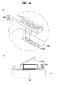
FIG. 1 shows one embodiment of a display device. -
FIG. 2 shows a cross-sectional view of the display device. -
FIG. 3 shows one embodiment of a backlight unit. -
FIG. 4 shows another embodiment of a backlight unit. -
FIGs. 5 to 8 show backlight unit which performs direct light emission. -
FIGs. 9 to 20 are views for explaining in more detail the backlight unit and display device according to the present invention; -
FIGs. 21 to 33 are views for explaining in more detail a base layer; and -
FIGs. 34 to 38 are views for explaining in more detail the configuration of the display device according to the present invention. - Reference will now be made in detail embodiments of the invention examples of which are illustrated in the accompanying drawings. Since the present invention may be modified in various ways and may have various forms, specific embodiments are illustrated in the drawings and are described in detail in the present specification. However, it should be understood that the present invention are not limited to specific disclosed embodiments, but include all modifications, equivalents and substitutes included within the spirit and technical scope of the present invention.
- The terms 'first', 'second', etc. may be used to describe various components, but the components are not limited by such terms. The terms are used only for the purpose of distinguishing one component from other components. For example, a first component may be designated as a second component without departing from the scope of the present invention. In the same manner, the second component may be designated as the first component.
- The term "and/or" encompasses both combinations of the plurality of related items disclosed and any item from among the plurality of related items disclosed.
- When an arbitrary component is described as "being connected to "or" being linked to" another component, this should be understood to mean that still another component(s) may exist between them, although the arbitrary component may be directly connected to, or linked to, the second component. In contrast, when an arbitrary component is described as "being directly connected to" or "being directly linked to" another component, this should be understood to mean that no component exists between them.
- The terms used in the present application are used to describe only specific embodiments or examples, and are not intended to limit the present invention. A singular expression can include a plural expression as long as it does not have an apparently different meaning in context.
- In the present application, the terms "include" and "have" should be understood to be intended to designate that illustrated features, numbers, steps, operations, components, parts or combinations thereof exist and not to preclude the existence of one or more different features, numbers, steps, operations, components, parts or combinations thereof, or the possibility of the addition thereof.
- Unless otherwise specified, all of the terms which are used herein, including the technical or scientific terms, have the same meanings as those that are generally understood by a person having ordinary knowledge in the art to which the present invention pertains. The terms defined in a generally used dictionary must be understood to have meanings identical to those used in the context of a related art, and are not to be construed to have ideal or excessively formal meanings unless they are obviously specified in the present application.
- The following embodiments of the present invention are provided to those skilled in the art in order to describe the present invention more completely. Accordingly, shapes and sizes of elements shown in the drawings may be exaggerated for clarity.
- Hereinafter, a liquid crystal display panel is used as an example of a display panel. Other display panels may be used. For example, a plasma display panel (PDP), a field emission display (FED) panel, and an organic light emitting diode (OLED) display panel may be used.
-
FIG. 1 shows one embodiment of adisplay device 1 which include afront cover 30, aback cover 40, and adisplay module 20 between thefront cover 30 and theback cover 40. - The
front cover 30 may cover thedisplay module 20 and may include a front panel (not shown) formed of a substantially transparent material capable of transmitting light. The front panel is positioned over a front surface of thedisplay module 20 to be spaced apart from the front surface of thedisplay module 20 at a predetermined distance, thereby protecting thedisplay module 20 from an external impact. -
FIG. 2 shows a cross-sectional view of the display device inFIG. 1 . As shown inFIG. 2 , thedisplay module 20 of thedisplay device 1 may include adisplay panel 100 and abacklight unit 200. - The
display panel 100 includes acolor filter substrate 110 and a thin film transistor (TFT)substrate 120 that are positioned opposite each other and are attached to each other with a uniform cell gap therebetween. A liquid crystal layer (not shown) may be interposed between thecolor filter substrate 110 and theTFT substrate 120. - The
color filter substrate 110 includes a plurality of pixels each including red (R), green (G), and blue (B) subpixels and may generate a red, green, or blue image when light is applied to the pixels. In this embodiment, each of the pixels includes the red, green, and blue subpixels. Other structures may be used for the pixel. For example, each pixel may include red, green, blue, and white (W) subpixels. - The
TFT substrate 120 includes one or more switching elements and may switch on and off corresponding pixel electrodes. - The liquid crystal layer is comprised of liquid crystal molecules. The arrangement of the liquid crystal molecules may vary depending on a voltage difference between a pixel electrode (not shown) and a common electrode (not shown). Hence, light provided by the
backlight unit 200 may be incident on thecolor filter substrate 110 based on changes in the arrangement of the liquid crystal molecules of the liquid crystal layer. - An upper
polarizing plate 130 and a lowerpolarizing plate 140 may be respectively positioned on an upper surface and a lower surface of thedisplay panel 100. More particularly, the upperpolarizing plate 130 may be positioned on an upper surface of thecolor filter substrate 110, and the lowerpolarizing plate 140 may be positioned on a lower surface of theTFT substrate 120. - A gate driver (not shown) and a data driver (not shown), each of which generates a driving signal for driving the
display panel 100, may be provided on the side of thedisplay panel 100. The above-described configuration of thedisplay panel 100 is merely one example; other configurations may be used for thedisplay panel 100. - As shown in
FIG. 2 , thedisplay module 20 may be configured so that thebacklight unit 200 adheres closely to thedisplay panel 100. For example, thebacklight unit 200 may be attached and fixed to the lower surface of thedisplay panel 100, more particularly the lowerpolarizing plate 140. For this, an adhesive layer (not shown) may be formed between the lowerpolarizing plate 140 and thebacklight unit 200. - As described above, because the
display device 1 is configured by closely attaching thebacklight unit 200 to thedisplay panel 100, the entire thickness of thedisplay device 1 may be reduced. Hence, an external appearance of thedisplay device 1 may be improved. - Further, because a structure for fixing the
backlight unit 200 is removed, the structure and the manufacturing process of thedisplay device 1 may be simplified. - Further, because a space between the
backlight unit 200 and thedisplay panel 100 is reduced, foreign substances may be prevented from penetrating into the space. Hence, a malfunction of thedisplay device 1 and a reduction in the image quality of thedisplay device 1 resulting from the foreign substances may be prevented. - In this embodiment, the
backlight unit 200 may have a structure in which a plurality of functional layers are sequentially stacked, and at least one of the plurality of functional layers may include a plurality of light sources (not shown). - Each of the plurality of functional layers constituting the
backlight unit 200 may be formed of a flexible material, so that thebacklight unit 200 is closely attached and fixed to the lower surface of thedisplay panel 100. Further, a frame (not shown) for stably positioning thebacklight unit 200 may be provided under thebacklight unit 200. - The
display panel 100 according to one embodiment may be divided into a plurality of regions. Brightness (i.e., brightness of the corresponding light source) of light emitted from a region of thebacklight unit 200 corresponding to each of the divided regions of thedisplay panel 100 is adjusted based on a gray peak value or a color coordinate signal of each divided region. Hence, a luminance of thedisplay panel 100 may be adjusted. For this, thebacklight unit 200 may operate, so that regions of thebacklight unit 200 respectively corresponding to the divided regions of thedisplay panel 100 are dividedly driven. -
FIG. 3 is a cross-sectional view of one embodiment of the backlight unit. As shown inFIG. 3 , thebacklight unit 200 may include asubstrate 210, a plurality oflight sources 220, aresin layer 230, and areflection layer 240. - The plurality of
light sources 220 may be formed on thesubstrate 210, and theresin layer 230 may be formed on thesubstrate 210 to cover thelight sources 220. - A connector (not shown) and an electrode pattern (not shown) for connecting the
light sources 220 to one another may be formed on thesubstrate 210. For example, a carbon nanotube electrode pattern (not shown) for connecting thelight sources 220 to the connector may be formed on an upper surface of thesubstrate 210. The connector may be electrically connected to a power supply unit (not shown) for supplying a power to thelight sources 220. - The
substrate 210 may be a printed circuit board (PCB) formed of polyethylene terephthalate (PET), glass, polycarbonate (PC), or silicon. Further, thesubstrate 210 may be a film substrate. - The
light source 220 may be one of a light emitting diode (LED) chip and a light emitting diode package having at least one light emitting diode chip. In the embodiment of the invention, the light emitting diode package is described as an example of thelight source 220. - The
light source 220 may be configured by a colored LED emitting at least one of red light, green light, blue light, etc. or a white LED emitting white light. In addition, the colored LED may include at least one of a red LED, a blue LED, and a green LED. The disposition and emitting light of the light emitting diode may be variously changed within a technical scope of the embodiment. - The
resin layer 230 positioned on thesubstrate 210 transmits light emitted from thelight sources 220, and at the same time diffuses the light emitted from thelight sources 220, thereby allowing thelight sources 220 to uniformly provide the light to thedisplay panel 100. - The
reflection layer 240 may be positioned between thesubstrate 210 and theresin layer 230, more particularly on the upper surface of thesubstrate 210. Thereflection layer 240 may reflect light emitted from thelight sources 220 and may again reflect light totally reflected from a boundary between theresin layer 230 and thereflection layer 240, thereby more widely diffusing the light emitted from thelight sources 220. - The
reflection layer 240 may select a sheet in which a white pigment, for example, titan white is dispersed, a sheet in which a metal deposition layer is stacked on the surface of the sheet, a sheet in which bubbles are dispersed so as to scatter light, etc. among various types of sheets formed of synthetic resin material. Silver (Ag) may be coated on the surface of thereflection layer 240 so as to increase a reflectance. Thereflection layer 240 may be formed by coating a resin on the upper surface of thesubstrate 210. - The
resin layer 230 may be formed of various kinds of resins capable of transmitting light. For example, theresin layer 230 may contain one or at least two selected from the group consisting of polyethylene terephthalate (PET), polycarbonate (PC), polypropylene, polyethylene, polystyrene, polyepoxy, silicon, acryl, etc. - Further, a refractive index of the
resin layer 230 may be approximately 1.4 to 1.6, so that thebacklight unit 200 has a uniform luminance by diffusing light emitted from thelight sources 220. - The
resin layer 230 may contain a polymer resin having an adhesion so as to tightly and closely adhere to thelight sources 220 and thereflection layer 240. For example, theresin layer 230 may contain an acrylic resin such as unsaturated polyester, methyl methacrylate, ethyl methacrylate, isobutyl methacrylate, normal butyl methacrylate, normal butylmethylmethacrylate, acrylic acid, methacrylic acid, hydroxy ethylmethacrylate, hydroxy propylmethacrylate, hydroxy ethylacrylate, acrylamide, methylol acrylamide, glycidyl methacrylate, ethylacrylate, isobutylacrlate, normal butylacrylate, 2-ethylhexyl acrylate polymer, copolymer, or terpolymer, etc., an urethane resin, an epoxy resin, a melamine resin, etc. - The
resin layer 230 may be formed by coating and curing a liquid or gel-type resin on the upper surface of thesubstrate 210 on which thelight sources 220 and thereflection layer 240 are formed. Alternatively, theresin layer 230 may be separately manufactured and then may be attached to the upper surface of thesubstrate 210. - As a thickness of the
resin layer 230 increases, light emitted from thelight sources 220 may be more widely diffused. Hence, thebacklight unit 200 may provide light having the uniform luminance to thedisplay panel 100. However, as the thickness of theresin layer 230 increases, an amount of light absorbed in theresin layer 230 may increase. Hence, the luminance of light which thebacklight unit 200 provides to thedisplay panel 100 may entirely decrease. Accordingly, the thickness of theresin layer 230 may be approximately 0.1 mm to 4.5 mm, so that thebacklight unit 200 can provide light having the uniform luminance to thedisplay panel 100 without an excessive reduction in the luminance of light. -
FIG. 4 shows another embodiment of the backlight unit. In this embodiment, the plurality oflight sources 220 may be mounted on thesubstrate 210, and theresin layer 230 may be disposed on the upper surface of thesubstrate 210. Thereflection layer 240 may be formed between thesubstrate 210 and theresin layer 230. - The
resin layer 230 may include a plurality of scatteringparticles 231. The scatteringparticles 231 may scatter or refract light incident on theresin layer 230, thereby more widely diffusing light emitted from thelight sources 220. - The scattering
particles 231 may be formed of a material having a refractive index different from a formation material of theresin layer 230 so as to scatter or refract the light emitted from thelight source 220. More particularly, the scatteringparticles 231 may be formed of a material having a refractive index greater than silicon-based resin or acrylic resin forming theresin layer 230. - For example, the scattering
particles 231 may be formed of polymethylmethacrylate (PMMA)/styrene copolymer (MS), polymethylmethacrylate (PMMA), polystyrene (PS), silicon, titanium dioxide (TiO2), and silicon dioxide (SiO2), or a combination thereof. Further, the scatteringparticles 231 may be formed of a material having a refractive index less than the formation material of theresin layer 230. - For example, the scattering
particles 231 may be formed by generating bubbles in theresin layer 230. Other materials may be used for the scatteringparticles 231. For example, thescattering particle 231 may be formed using various polymer materials or inorganic particles. - In this embodiment, scattering
particles 231 may be formed of a material having a refractive index than less a formation material ofresin layer 230. For example, the scatteringparticles 231 may be formed by forming bubbles in theresin layer 230. A formation material of the scatteringparticles 231 is not limited to the above-described material and may be formed of various polymer materials or various inorganic materials. - In one embodiment, the
resin layer 230 may be formed by mixing the liquid or gel-type resin with the scatteringparticles 231 and then coating and curing a mixture on the upper surface of thesubstrate 210 on which thelight sources 220 and thereflection layer 240 are formed. - As shown in
FIG. 4 , anoptical sheet 250 may be disposed on the top of thesecond layer 230. Theoptical sheet 250 may include at least oneprism sheet 251 and/or at least onediffusion sheet 252. In this instance, a plurality of sheets constitutingoptical sheet 250 are not separated from one another and are attached to one another. Thus, the thickness of theoptical sheet 250 or the thickness of thebacklight unit 200 may be reduced. - A lower surface of the
optical sheet 250 may closely adhere to theresin layer 230, and an upper surface of theoptical sheet 250 may closely adhere to the lower surface of thedisplay panel 110, i.e., the lowerpolarizing plate 140. - The
diffusion sheet 252 may diffuse incident light to thereby prevent light coming from theresin layer 230 from being partially concentrated. Hence, thediffusion sheet 252 may further uniformize the luminance of light. Further, theprism sheet 251 may focus light coming from thediffusion sheet 252, thereby allowing the light to be vertically incident on thedisplay panel 110. - In one embodiment, at least one of the
prism sheet 251 anddiffusion sheet 252 constituting theoptical sheet 250 may be removed. Theoptical sheet 250 may further include other functional layers in addition to theprism sheet 251 and thediffusion sheet 252. - In a backlight unit which performs direct light emissions, an LED package constituting the
light sources 220 may be classified into a top view type LED package and a side view type LED package based on a facing direction of a light emitting surface of the LED package. -
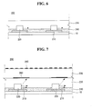
FIGs. 5 to 8 illustrate a backlight unit which performs direct light emissions. More specifically,FIGs. 5 and6 respectively illustrate a top view type LED package and a side view type LED package in the direct light emitting manner of the backlight unit. - As shown in
FIG. 5 , each of the plurality oflight sources 220 of thebacklight unit 200 has a light emitting surface on an upper surface of eachlight source 220. Thus, the plurality oflight sources 220 may emit light in an upward direction, for example, in a direction perpendicular to thesubstrate 210 or thereflection layer 240. - As shown in
FIG. 6 , each of the plurality oflight sources 220 of thebacklight unit 200 has the light emitting surface at the side of eachlight source 220. Thus, the plurality oflight sources 220 may emit light in a lateral direction, for example, an extension direction of thesubstrate 210 or thereflection layer 240. For example, the plurality oflight sources 220 may be configured using the side view type LED package. As a result, it is possible to reduce a problem that thelight sources 220 are observed as a hot spot on the screen of thedisplay panel 100. Furthermore, the thin profile of thedisplay device 1 may be achieved because of a reduction of the thickness "a" of theresin layer 230. - As shown in
FIG. 7 , thebacklight unit 200 may include a plurality ofresin layers FIG. 7 , light emitted from the side of thelight source 220 may be transmitted by thefirst resin layer 230 and may travel in a formation area of alight source 225 adjacent to thelight source 220. - A portion of light transmitted by the
first resin layer 230 may be emitted in an upward direction corresponding to a direction of thedisplay panel 100. For this, thefirst resin layer 230 may include a plurality of scatteringparticles 231 as described above with reference toFIG. 4 and may scatter or refract light travelling in the upward direction - A portion of light emitted from the
light source 220 may be incident on thereflection layer 240, and the light incident on thereflection layer 240 may be reflected and diffused in the upward direction. - A large amount of light may be emitted in an area around the
light source 220 because of a strong scattering phenomenon around thelight source 220 or light emitted from thelight source 220 in a direction similar to the upward direction. Hence, light having a high luminance may be observed on the screen. - To prevent this, as shown in
FIG. 7 , a firstlight shielding pattern 260 may be formed on thefirst resin layer 230 to reduce a luminance of light emitted in an area around thelight source 220. Hence, thebacklight unit 200 may emit light having the uniform luminance. For example, the firstlight shielding pattern 260 may be formed on thefirst resin layer 230 corresponding to the formation area of the plurality oflight sources 220 to shield a potion of light from thelight source 220 and to transmit a portion of the remaining light. Hence, the firstlight shielding pattern 260 may reduce the luminance of light emitted upward. - The first
light shielding pattern 260 may be formed of titanium dioxide (TiO2). In this instance, the firstlight shielding pattern 260 may reflect downward a potion of light from thelight source 220 and may transmit a portion of the remaining light. - In one embodiment, a
second resin layer 235 may be disposed on thefirst resins layer 230. Thesecond resin layer 235 may be formed of the same material as or a different material from thefirst resins layer 230. Thesecond resin layer 235 may diffuse light upward emitted from thefirst resins layer 230, thereby improving the uniformity of the luminance of light from thebacklight unit 200. - The
second resin layer 235 may be formed of a material having a refractive index equal to or different from the refractive index of the formation material of thefirst resins layer 230. When thesecond resin layer 235 is formed of the material having the refractive index greater than the refractive index of thefirst resins layer 230, thesecond resin layer 235 may widely diffuse light from thefirst resin layer 230. - When the
second resin layer 235 is formed of the material having the refractive index less than the refractive index of thefirst resin layer 230, light from thefirst resin layer 230 may increase a reflectance of light reflected from a lower surface of thesecond resin layer 235. Hence, light from thelight source 220 may easily travel along thefirst resin layer 230. - Each of the
first resin layer 230 and thesecond resin layer 235 may include a plurality of scattering particles. In this instance, a density of the scattering particles of thesecond resin layer 235 may be greater than a density of the scattering particles of thefirst resin layer 230. When thesecond resin layer 235 includes the scattering particles having the density greater than thefirst resin layer 230, thesecond resin layer 235 may widely diffuse light upward emitted from thefirst resin layer 230. Hence, the uniformity of the luminance of light from thebacklight unit 200 may be improved. - As shown in
FIG. 7 , a secondlight shielding pattern 265 may be formed on thesecond resin layer 235 to uniformize the luminance of light from thesecond resin layer 235. For example, when light upward emitted from thesecond resin layer 235 is concentrated in a specific potion and thus is observed on the screen as the light having the high luminance, the secondlight shielding pattern 265 may be formed in an area corresponding to a specific potion of an upper surface of thesecond resin layer 235. Hence, because the secondlight shielding pattern 265 may reduce the luminance of light in the specific potion, the luminance of light emitted from thebacklight unit 200 may be uniform. - The second
light shielding pattern 265 may be formed of titanium dioxide (TiO2). In this instance, the secondlight shielding pattern 265 may reflect downward a potion of light from thesecond resin layer 235 and may transmit a portion of the remaining light. - As shown in
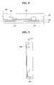
FIG. 8 , a pattern may be formed on thereflection layer 240, thereby facilitating a travel of light emitted from thelight source 220 to thelight source 225 adjacent to thelight source 220. The pattern on an upper surface of thereflection layer 240 may include a plurality ofprotrusions 241. Light that is emitted from thelight source 220 and then is incident on the plurality ofprotrusions 241 may be scattered or refracted in a direction indicated by an arrow ofFIG. 8 . - As shown in
FIG. 8 , a density of theprotrusions 241 formed on thereflection layer 240 may increase as a separated distance between theprotrusions 241 and thelight source 220 increases (i.e., as theprotrusions 241 are close to the light source 225). Hence, a reduction in a luminance of upward emitted light in an area distant from the light source 220 (i.e., in an area near to the light source 225) may be prevented. As a result, the luminance of light provided by thebacklight unit 200 may be uniformized. - The
protrusions 241 may be formed of the same material as thereflection layer 240. In this instance, theprotrusions 241 may be formed by processing the upper surface of thereflection layer 240. Alternatively, theprotrusions 241 may be formed of a material different from thereflection layer 240. In this instance, theprotrusions 241 may be formed by printing the pattern on the upper surface of thereflection layer 240. The shape of theprotrusions 241 is not limited to a shape shown inFIG. 8 and may be variously changed. For example, other shapes such as a prism shape may be used. -
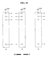
FIGs. 9 to 20 are views for explaining in more detail the backlight unit and display device according to the present invention. It is noted that the description of parts which have been described in detail above will be omitted. For example, thelight shielding pattern 260, protrusions, etc. that have been described in detail above can be applied to the following configuration. Also,light sources 220 to be described below may be at least one of a side-view type and a top-view type. - Referring to
FIG. 9 , a plurality oflight sources 220 may be disposed on asubstrate 210. For example, a plurality oflight sources 210 can be disposed in a stripe type on asubstrate 210. In other words, a plurality oflight sources 220 can be disposed in a straight line on asubstrate 210. - Moreover, a
transmission line 2400 for transmitting a driving signal supplied from an external driver may be formed on thesubstrate 220. Thetransmission line 2400 may be an electrode pattern. - The
transmission line 2400 or electrode pattern of this type has been described above inFIG. 3 . - In addition, a
connector 900 for connecting a cable (not shown) may be disposed on thesubstrate 210 to electrically connect an external driver to thesubstrate 210 where thelight sources 220 are disposed. - A plurality of
substrates 210 of this type may be disposed on a base layer. - For example, as shown in
FIG. 10 , a plurality ofsubstrates 210 may be disposed, separated from each another, on thebase layer 10. Preferably, a plurality ofsubstrates 210 may be disposed in parallel, separated from each other, on thebase layer 10. - Referring to
FIG. 10 , thefirst substrate 211,second substrate 212, andthird substrate 213, among the plurality ofsubstrates 210, may be disposed, separated from each other at a predetermined distance, on thebase layer 10. - Here, the distance between two
adjacent substrates 210, for example, the gap R1 between thefirst substrate 211 and thesecond substrate 212, may be greater than the width of onesubstrate 210, for example, the width R2 of thefirst substrate 211. - In contrast to the present invention, a comparative example in which the
base layer 10 is not used will be described below with reference toFIG. 11 . - Referring to
FIG. 11 , in a display device according to the comparative example, a plurality oflight sources 220 may be disposed on asubstrate 210. Also, areflection layer 240 may be disposed on top of thesubstrate 210, and aresin layer 230 may be disposed on top of thereflection layer 240. - In this case, the size of the
substrate 210 may be excessively increased, and accordingly the manufacturing cost may be excessively increased, and the workability of an operation for disposing/forming a plurality oflight sources 220 andtransmission lines 2400 on thesubstrate 210 may become poor. - On the other hand, in the case that a plurality of
substrates 210 are disposed on thebase layer 10 as in the present invention, the size of therespective substrates 210 may be reduced, thereby lowering the manufacturing cost. Also, the workability of a manufacturing process of therespective substrates 210 may be excellent because the number oftransmission lines 2400 andlight sources 220 formed/disposed on therespective substrates 210 in the manufacturing process is relatively small. - Moreover, the
base layer 10 may be made of a rather cheap material because thetransmission lines 2400 and thelights sources 220 are formed on thebase layer 10, thereby further reducing the manufacturing cost. - Referring to
FIG. 12 , anadhesive layer 300 may be disposed between thebase layer 10 and thesubstrates 210. Theadhesive layer 300 can attach thesubstrates 210 to thebase layer 10, and also can transmit light generated from thesubstrates 210 and/or thelight sources 200 to thebase layer 10. To this end, theadhesive layer 300 can include a thermally conductive material, for example, metal particles. - Referring to
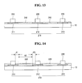
FIG. 13 , thereflection layer 240 may include portions disposed on the surface of thebase layer 10. For example, thereflection layer 240 may include portions disposed in the area between twoadjacent substrates 210. - Alternatively, as shown in
FIG. 14 , thereflection layer 240 may include portions A2 disposed on the surface of thebase layer 10 and portions A1 and A3 overlapping with thesubstrates 210. Here, the portions A1 and A3 overlapping with thesubstrates 210 may be portions disposed on the surfaces of thesubstrates 210. Also, the portions A2 disposed on the surface of thebase layer 10 may be portions overlapping with thebase layer 10. The portions A2 of thereflection layer 240 overlapping with thebase layer 10 may be in contact with thebase layer 10. - In this case, the width of the portions A2 of the
reflection layer 240 disposed on the surface of thebase layer 10 may be greater than the width of the portions A1 and A3 overlapping with thesubstrates 210. - Meanwhile, the plurality of
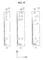
light sources 220 disposed on thesubstrates 210 may be arranged in various patterns. - For example, as shown in (A) of
FIG. 15 , a plurality oflight sources 220 may be disposed in a straight line on asubstrate 210. In this case, it can be viewed that the plurality oflight sources 220 disposed on thesubstrate 210 are arranged in a vertical direction DRV. - Alternatively, as shown in (B) of
FIG. 15 , a plurality oflight sources 220 may be arranged along a plurality of rows on asubstrate 210. In this case, it can be viewed that at least twolight sources 220 are arranged on thesubstrate 210 in the vertical direction DRV, and at least two of the remaininglight sources 220 are arranged thereon in a horizontal direction DRH. Here, it is not necessary for the vertical direction DRV and the horizontal direction DRH to be orthogonal. - Alternatively, as shown in (C) of
FIG. 15 , it can be viewed that at least twolight sources 220 are arranged on thesubstrate 210 in the vertical direction DRV, and at least two of the remaininglight sources 220 are arranged in a diagonal direction between the vertical direction DRV and the horizontal direction DRH. In this case, it can be viewed that the plurality oflight sources 220 are arranged in a zigzag form. - As shown in
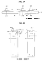
FIG. 16 , thelight source 220 may include alight emitting face 600 for emitting light. As a predetermined light can be emitted from thelight emitting face 600, the direction toward which thelight emitting face 600 faces can be regarded as a light emitting direction. - Referring to
FIG. 17 , the light emitting directions of the plurality oflight sources 220 disposed on asubstrate 210 may be all the same. For example, if thelight sources 220 are of the side-view type,light sources 220 for emitting light in the same direction may be disposed on apredetermined substrate 220. - Alternatively, the light emitting directions of the
light sources 220 disposed on twopredetermined substrates 210 among the plurality oflight sources 220 may be different. In other words, the light emitting direction of the light sources disposed on the first substrate among the plurality ofsubstrates 210 may be different from the light emitting direction of the light sources disposed on the second substrate, which is different from the first substrate. - For example, as shown in
FIG. 18 , thefirst light sources 221 disposed on thefirst substrate 210A among the plurality ofsubstrates 210 may emit light in the first direction DR1, and the secondlight sources 222 disposed on thesecond substrate 210B adjacent to thefirst substrate 210A may emit light in the second direction DR2 different from the first direction DR1. Here, the first direction DR1 and the second direction DR2 may be opposite to each other. - Moreover, the third
light sources 223 disposed on thethird substrate 210C adjacent to thesecond substrate 210B may emit light in the first direction DR1. - In this case, it is possible to prevent a noise image of a specific pattern from being displayed on a screen along the light emitting direction.
- As such, if the light emitting directions of the
light sources 220 disposed ondifferent substrates 210 are different from each other, the gaps between thesubstrates 210 may be different. - For example, as shown in
FIG. 19 , in the case that thefirst light sources 221 disposed on thefirst substrate 210A emit light in the first direction DR1, i.e., the direction facing thesecond substrate 210B, the secondlight sources 222 disposed on thesecond substrate 210B emit light in the second direction DR2 different from the first direction DR1, i.e., the direction facing thefirst substrate 210A, and the thirdlight sources 223 disposed on thethird substrate 210C adjacent to thesecond substrate 210B emit light in the first direction DR1, i.e., the direction becoming distant from thesecond substrate 210B, the gap R3 between thefirst substrate 210A and thesecond substrate 210B may be greater than the gap R4 between thesecond substrate 210B and thethird substrate 210C. - In this case, it is possible to prevent a noise image of a specific pattern from being displayed on a screen along the light emitting direction, and to prevent a hot-spot phenomenon in which the luminance of a specific region is higher than the luminance of other regions.
- Alternatively, the light emitting direction of at least one of the plurality of
light sources 220 disposed on asubstrate 210 may be different from the light emitting direction of at least one of the remaininglight sources 220. - For example, as shown in
FIG. 20 , the firstlight source 220A disposed on the first substrate 210-1 may emit light in the first direction DR1, and the second lights source 220B may emit light in the second direction DR2 different from the first direction DR1. - Here, if the gap S1 between the first
light source 220A and the second substrate 210-2 adjacent to the first substrate 210-1 is greater than the gap S2 between the secondlight source 220B and the second substrate 210-2, the firstlight source 220A may emit light in the direction facing thesecond substrate 220B, and the secondlight source 220B may emit light in the direction becoming distant from thesecond substrate 220B. -
FIGs. 21 to 33 are views for explaining in more detail the base layer. It is noted that the description of parts which have been described in detail above will be omitted. - The thickness of the
base layer 10 may vary according to its position. - For example, as shown in
FIG. 21 , the thickness T12 of thebase layer 10 at a position corresponding to the region between twoadjacent substrates 210 may be greater than the thickness T11 of thebase layer 10 in the region overlapping with thesubstrate 210. In other words, the thickness T11 of thefirst portion 10A of thebase layer 10 overlapping with thesubstrate 210 may be less than the thickness T12 of thesecond portion 10B not overlapping with thesubstrate 210. - To this end, a plurality of
grooves 11 may be formed in thebase layer 10, and therespective substrates 210 may be positioned in thegrooves 11. - In this way, in the case that the
grooves 11 are formed in thebase layer 10, and thesubstrates 210 are inserted into thegrooves 11, thesubstrates 210 may be fixed to thebase layer 10 without the use of any adhesive layer. Therefore, the adhesive layer between thebase layer 10 and thesubstrates 210 may be omitted. - As such, in order to fix the plurality of
substrates 210 to thebase layer 10, the plurality ofgrooves 11 may be formed in parallel in thebase layer 10 as shown inFIG. 22 . - For example, it is assumed that the
base layer 10 has an approximately rectangular shape, and thebase layer 10 includes a first long side LS1, a second long side LS2 facing the first long side LS1, a second short side SS2 adjacent to the first long side LS1 and the second long side LS2, and a first short side SS1 facing the second short side SS2. In this case, the plurality ofgrooves 11 may be formed in parallel to the first and second short sides SS1 and SS2 of thebase layer 10. - Here, the depth of the
grooves 11 may be less than the height of thesubstrates 210. For example, as shown inFIG. 23 , the depth T1 of thegroove 11 formed in thebase layer 10 may be less than the height T2 of thesubstrate 210 inserted into thegroove 11. In this case, thesubstrate 210 may be protruded by a predetermined height from thebase layer 10. - Moreover, the
reflection layer 240 may include portions positioned on the surface of thebase layer 10 and portions positioned on the surface of thesubstrate 210. Also, thereflection layer 240 may be spaced apart by a predetermined distance G1 from thelight source 220. - Alternatively, as shown in
FIG. 24 , the depth T1 of thegroove 11 formed in thebase layer 10 may be greater than the height T2 of thesubstrate 210 inserted into thegroove 11. In this case, thesubstrate 210 may be positioned lower than the surface of thebase layer 10. - Even with this structure, the
reflection layer 240 may include portions positioned on the surface of thebase layer 10 and portions positioned on the surface of thesubstrate 210. - Alternatively, as shown in
FIG. 25 , if the depth T1 of thegroove 11 is further increased, the depth T1 of thegrooves 11 may be greater than the height T4 from the bottom of thesubstrate 210 to the top of thelight source 220. That is, the depth T1 of thegroove 11 may be greater than the height T3 measured from the bottom of thesubstrate 220 to the top of thelight source 220. Moreover, the thickness T12 of thesecond portion 10B of thebase layer 10 is greater than the distance T4 from the bottom of thebase layer 10 to the top of thelight source 220. - With this structure, as shown in
FIG. 26 , it is possible to form aresin layer 230 surrounding thesubstrate 210 and thelight source 220. - In this case, the
resin layer 230 may include a portion positioned within thegroove 11. - Moreover, the
resin layer 230 may include portions AR1 and Ar2 positioned on top of thebase layer 10. In this case, part of theresin layer 230 may be in contact with thebase layer 10. For example, the portions AR1 and AR2 of theresin layer 230 positioned on top of thebase layer 10 may be in contact with thebase layer 10. - With this structure, in the case that the
light source 220 is the side-view type that emits light laterally, thebase layer 10 may be formed of a substantially transparent material. - Meanwhile, the
resin layer 230 may include a recessed portion in the region corresponding to thegroove 11 of thebase layer 10. - For example, as shown in
FIG. 27 , theresin layer 230 may include a recessedportion 230A whose surface is recessed by a predetermined depth T20 toward the bottom of thebase layer 10. In this case, light emitted from thelight sources 220 may be diffused more widely due to the difference in the reflective index among a plurality of functional layers positioned on top of thelight source 220. - Alternatively, as shown in
FIG. 28 , theresin layer 230 may include a portion in which the depth T5 measured from the bottom of thebase layer 10 to the surface of theresin layer 230 is less than the maximum thickness T12 of thebase layer 10. In other words, theresin layer 230 may include a portion lowered by a predetermined depth T21 from the surface of thebase layer 10. - In this case, the
resin layer 230 may be positioned substantially within thegroove 11 of thebase layer 10. Also, the portions of thebase layer 10, other than thegroove 11, may not be blocked by theresin layer 230. - Meanwhile, the
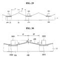
base layer 10 may include a portion whose thickness gradually changes in the region between twoadjacent substrates 210. Here, agroove 11 where thesubstrate 210 is disposed may be formed in thebase layer 10, or thegroove 11 may not be formed therein. The following description will be made under the assumption that thegroove 11 is formed in thebase layer 10. - For example, as shown in
FIG. 29 , thesecond portion 10B disposed in the region between thefirst substrate 2900 andsecond substrate 2910 disposed on thebase layer 10 may include a portion whose thickness gradually increase from thefirst portion 10A toward the center P of thesecond portion 10B. Here, the thickness of thebase layer 10 may increase as the left region IP of thesecond portion 10B goes from thefirst substrate 2900 toward the center P of thesecond portion 10B, and the thickness of thebase layer 10 may increase as the right region DP of thesecond portion 10B goes from thesecond substrate 2910 toward the center P of thesecond portion 10B. - Alternatively, when the position at which the thickness of the
second portion 10B of thebase layer 10 is maximum, i.e., the position having the maximum thickness in the region between thefirst substrate 2900 andsecond substrate 2910 on thebase layer 10 is referred to as the first position P, thesecond portion 10B may include a portion whose thickness increases toward the first position P. - With this structure, the
light sources 220 may emit light in the direction facing thesecond portion 10B of thebase layer 10. - For example, as shown in
FIG. 30 , thefirst light source 2901 disposed on thefirst substrate 2900 may emit light in the direction facing the left region IP of thesecond portion 10B, and the secondlight source 2902 disposed on thesecond substrate 2910 may emit light in the direction facing the right region DP of thesecond portion 10B. - In this case, the light emitted from the
first light source 2901 and the light emitted from the secondlight source 2902 may be reflected toward the front (the direction in which an image is displayed) in the portion of thereflection layer 240 corresponding to thesecond portion 10B of thebase layer 10, and accordingly the optical characteristics may be improved. More specifically, the loss of the light emitted from thefirst light source 2901 and the secondlight source 2902 can be reduced, thus improving luminance and enhancing light efficiency. - Moreover, the height of the position at which the thickness of the
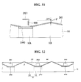
second portion 10B of thebase layer 10 is maximum, i.e., the first position, may be less than the maximum height of thelight sources 220. That is, the height measured from the bottom of thebase layer 10 to the top of the first position P of thesecond portion 10B may be less than the height measured from the bottom of thebase layer 10 to the top of thelight sources 220. In this case, a hot spot phenomenon where light is concentrated at the first position P may be reduced. - More specifically, as shown in
FIG. 31 , the maximum height of thelight emitting face 600 of thelight source 220 measured from the bottom of thebase layer 10, i.e., thefirst light source 2901, may be greater than the height measured from the bottom of thebase layer 10 to the top of the first position P of thesecond portion 10B. - Alternatively, as shown in
FIG. 32 , the height of the position at which the thickness of thesecond portion 10B of thebase layer 10 is maximum, i.e., the first position, may be greater than the maximum height of thelight sources 220. That is, the height measured from the bottom of thebase layer 10 to the top of the first position P of thesecond portion 10B may be greater than the height measured from the bottom of thebase layer 10 to the top of thelight sources 220. - In this case, the
resin layer 230 covering thesubstrates 2900t0 2920 and thelight sources 2901 to 2903 may not be positioned at the first position P of thesecond portion 10B of thebase layer 10. In other words, thesecond portion 10B may include portions not covered by theresin layer 230. Also, thereflection layer 240 may include portions not covered by theresin layer 230. - Alternatively, as shown in
FIG. 33 , the rate of change in thickness per unit distance of thebase layer 10 between the first position P of thesecond portion 10B of thebase layer 10 and thefirst substrate 2900 may be less than the rate of change in thickness per unit distance of thebase layer 10 between the first position P and thesecond substrate 2910. In other words, the slope of thebase layer 10 between the first position P of thesecond portion 10B of thebase layer 10 and thefirst substrate 2900 is slower than the slope of thebase layer 10 between the first position P and thesecond substrate 2910. - In this case, the
first light source 2901 disposed on thefirst substrate 2900 may emit light in the direction facing thesecond portion 10B, and the secondlight source 2902 disposed on thesecond substrate 2910 may emit light in the direction becoming distant from thefirst light source 2901. - In this case, the optical characteristics may be further improved.
-
FIGs. 34 to 38 are views for explaining in more detail the configuration of the display device according to the present invention. It is noted that the description of parts which have been described in detail above will be omitted. - Referring to
FIG. 34 , the display device according to the present invention may include adisplay module 20, aframe 14, a drivingboard 15, and aback cover 40. - The
display module 20 has been previously described in detail. - The
frame 140 may be disposed at the back of thedisplay module 20, more specifically, at the back of abacklight unit 200. Theframe 14 can provide a holding power for supporting thebacklight unit 200. - The driving
board 15 may be disposed at the back of theframe 14. The drivingboard 15 can supply a driving signal to the electrodes of adisplay panel 10 included in thedisplay module 20. Also, the drivingboard 15 can supply a driving signal to thebacklight unit 200. Specifically, the drivingboard 15 can supply a driving signal to thelight sources 220 of thebacklight unit 200. - The
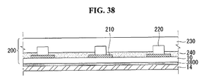
back cover 40 may be disposed at the back of the drivingboard 15. - Moreover, as shown in
FIG. 35 , thelight sources 220 may be disposed at the front surface of thesubstrate 210, and aconnector 900 may be disposed at the back of thesubstrate 210. - The
connector 900 may be electrically connected to at least onelight source 220 disposed at the front surface of thesubstrate 210. Accordingly, theconnector 900 electrically connects an external driver, i.e., a driving circuit, though not shown, and thelight sources 220, thereby enabling the driving circuit to supply a driving voltage to thelight sources 220. - In addition, the
connector 900 may include afirst portion 910, afirst electrode 930, and asecond portion 920. Here, thefirst portion 910 may be fixed to the back surface of thesubstrate 210. Thefirst electrode 930 may be formed on thefirst portion 910, and connected to a cable (not shown). Thesecond portion 920 may apply pressure such that the cable is electrically attached to thefirst electrode 930. Furthermore, the cable electrically connected to thefirst electrode 930 is brought into electrical contact with an external driving circuit, and as a result, thelight source 220 and the external driving circuit may be electrically connected to each other -
FIG. 35 illustrates one example of the structure of theconnector 900, and the present invention is not limited to theconnector 900 ofFIG. 35 . For instance, in the present invention, thesecond portion 920 may be omitted, and the cable not shown may be attached to thefirst portion 910 with an anisotropic adhesive containing conductive balls. In this case, thefirst electrode 930 of theconnector 900 and the cable may be electrically connected to each other by the conductive balls. - Alternatively, as shown in
FIG. 36 , theconnector 900 may be electrically connected to thesecond electrode 1100 formed on thesubstrate 210. Specifically, thesecond electrode 1100 may be formed on the back surface of thesubstrate 210, and the third electrode 940 may be formed on the bottom face of thefirst portion 910. Thesecond electrode 1100 and the third electrode 940 may be electrically connected. - As such, in order to electrically connect the third electrode 940 of the
connector 900 and thesecond electrode 1100 formed on thesubstrate 210, an adhesive layer 1110 may be formed between theconnector 900 and the back surface of thesubstrate 210, and the adhesive layer 1110 may containconductive particles 1111. Here, theconductive particles 1111 may be conductive balls, and, although not shown, may consist of a core made of a metallic material, such as silver Ag, and a coating coated around the core. The coating may include a material, such as carbon. - The third electrode 940 of the
connector 900 and thesecond electrode 1100 formed on thesubstrate 210 may be electrically connected by theconductive particles 1111 contained in the adhesive layer 1110. - Moreover, the
first electrode 930 and second connector 940 of theconnector 900 may be connected to each other. - In addition, the
second electrode 1100 disposed on the back surface of thesubstrate 210 may be electrically connected to thelight sources 220 disposed on the front surface of thesubstrate 210. - Accordingly, when the cable is connected to the
first electrode 930 of theconnector 900, thelight sources 220 disposed on the front surface of thesubstrate 210 and the cable can be electrically connected. - Moreover, as shown in
FIG. 37 , ahole 3600 may be formed in thebase layer 10. Thehole 3600 formed in thebase layer 10 is referred to as thefirst hole 3600. - In addition, the
connector 900 disposed on thesubstrate 210 may be disposed at a position corresponding to thefirst hole 3600. Also, asecond hole 3610 may be formed in theframe 14. - Furthermore, the
cable 3620 for electrically connecting the drivingboard 3630 disposed at the back of theframe 14 and thelight source 220 disposed on thesubstrate 210 may pass through thefirst hole 3600 and the second hole 36710. Accordingly, the drivingboard 3630 and thelight sources 220 can be electrically connected. - Moreover, as shown in
FIG. 38 , an adhesive layer 3800 may be disposed between thebacklight unit 200 and theframe 14. Specifically, the adhesive layer 3800 may be formed between thebase layer 10 of thebacklight unit 200 and theframe 14. In this case, the thickness of the display device can be reduced by bringing thebacklight unit 200 and the frame into further contact with each other. - The following description pages 22 to 23 contain preferred embodiments. Accordingly, the term "claim" as used therein refers to such a "preferred embodiment".
- 1. A backlight unit comprising:
- a base layer;
a plurality of substrates disposed on the base layer and separated from each other; and
light sources disposed on each of the substrates.
- a base layer;
- 2. The backlight unit of
claim 1, wherein a plurality of grooves are formed in the base layer, and the substrates are positioned in the grooves. - 3. The backlight unit of claim 2 wherein the depth of the grooves is greater than the height from the bottom of the substrates to the top of the light sources.
- 4. The backlight unit of claim 2, wherein the depth of the grooves is less than the thickness of the substrates.
- 5. The backlight unit of claim 2, wherein a hole is formed in each groove.
- 6. The backlight unit of
claim 1, further comprising a resin layer covering the substrates and the light sources. - 7. The backlight unit of claim 6, the resin layer comprises portions positioned on top of the base layer.
- 8. The backlight unit of claim 6, wherein the resin layer comprises a portion in which the height measured from the bottom of the base layer is less than the maximum thickness of the base layer.
- 9. The backlight unit of
claim 1, further comprising a reflection layer disposed on top of the base layer. - 10. The backlight unit of
claim 1, wherein the substrates comprise:- a first substrate where a plurality of light sources are disposed; and
- a second substrate disposed in parallel to the first substrate and having a plurality of light sources disposed thereon.
- 11. The backlight unit of
claim 10, wherein the gap between the first substrate and the second substrate is greater than the width of the first substrate or the width of the second substrate. - 12. The backlight unit of
claim 10, wherein the thickness of the portion of the base layer overlapping with the first substrate and the thickness of the portion overlapping with the second substrate are less than the thickness of the region between the first substrate and the second substrate. - 13. The backlight unit of
claim 10, wherein the light emitting direction of the light sources disposed on the first substrate is different from the light emitting direction of the light sources disposed on the second substrate. - 14. A display device comprising:
- a display panel;
- a backlight unit disposed at the back of the display panel; and
- a back cover disposed at the back of the backlight unit,
- the backlight unit comprising:
- a base layer;
- a plurality of substrates disposed on the base layer and separated from each other; and
- light sources disposed on the substrates.
- 15. The display device of
claim 14, further comprising a frame disposed at the back of the base layer.
Claims (15)
- A display device comprising:a base layer (10) comprising at least one hole (3600);a plurality of substrates (210, 211, 212, 213) disposed on a first side of the base layer (10) and separated from each other;a plurality of light sources (220) disposed on each of the substrates (210);a first connector (900) disposed on each of the substrates (210);a plurality of transmission lines (2400) disposed on each of the substrates (210) and configured to electrically connect the first connector (900) and the light sources (220);a driving board (3630) disposed on the second side of the base layer (10) and configured to supply a driving signal to the light sources (220), the second side of the base layer (10) being an opposite side of the first side of the base layer (10); anda second connector (3620) configured to electrically connect the first connector (900) and the driving board (3630) through the hole;optical sheet (250) disposed above the light sources; anda display panel (100) disposed above the optical sheet (250).
- The display device of claim 1, wherein a gap between a first substrate and a second substrate of the substrates (210) is greater than a width of each of the substrates (210).
- The display device as claimed in any one of claims 1 or 2, wherein the first connector (900) is disposed on each of the substrates (210) in a same side of the light sources (220).
- The display device as claimed in any one of claims 1 to 3, further comprising an adhesive layer (300) disposed between the base layer (10) and the substrates (210).
- The display device as claimed in any one of claims 1 to 4, further comprising a reflection layer (240) disposed on the surface of the base layer (10),
wherein the reflection layer (240) comprises:a first portion (A1) overlapping with the substrates (210); anda second portion (A2) overlapping with the base layer (10). - The display device of claim 5, wherein a width of the first portion (A1) is less than a width of the second portion (A2).
- The display device as claimed in any one of claims 1 to 6, wherein the first connector (900) is disposed on each of the substrates (210) in an opposite side of the light sources (220).
- The display device as claimed in any one of claims 5 to 7, further comprising:a first resin layer (230) covering the substrates (210) and the light sources (220); anda first shielding pattern (260) disposed on the first resin layer (230).
- The display device of claim 8, further comprising:a second resin layer (235) covering the first resin layer (230) and the first shielding pattern (260); anda second shielding pattern (265) disposed on the second resin layer (235).
- The display device as claimed in any one of claims 1 to 9, wherein the second connector (3620) is a cable.
- The display device as claimed in any one of claims 1 to 10, wherein a plurality of grooves (11) are formed in the base layer (10), and the substrates (210) are positioned in the grooves (11).
- The display device of claim 11, wherein a depth of the grooves (11) is greater than the height from the bottom of the substrates (210) to the top of the light sources (220).
- The display device of claim 12, wherein a depth of the grooves (11) is less than the thickness of the substrates (210).
- The display device as claimed in any one of claims 12 or 13, wherein a depth of the grooves (11) is less than a height of the substrates (210).
- The display device of as claimed in any one claim 5 to 14, wherein the first portion (A1) of the reflection layer (240) is spaced apart by a predetermined distance (G1) from the light sources (220).
Applications Claiming Priority (2)
| Application Number | Priority Date | Filing Date | Title |
|---|---|---|---|
| KR1020110000965A KR101771557B1 (en) | 2011-01-05 | 2011-01-05 | Display Apparatus |
| EP12000039.3A EP2474857B1 (en) | 2011-01-05 | 2012-01-04 | Backlight unit |
Related Parent Applications (2)
| Application Number | Title | Priority Date | Filing Date |
|---|---|---|---|
| EP12000039.3A Division EP2474857B1 (en) | 2011-01-05 | 2012-01-04 | Backlight unit |
| EP12000039.3A Division-Into EP2474857B1 (en) | 2011-01-05 | 2012-01-04 | Backlight unit |
Publications (3)
| Publication Number | Publication Date |
|---|---|
| EP2889677A2 true EP2889677A2 (en) | 2015-07-01 |
| EP2889677A3 EP2889677A3 (en) | 2015-08-12 |
| EP2889677B1 EP2889677B1 (en) | 2018-06-20 |
Family
ID=45491377
Family Applications (2)
| Application Number | Title | Priority Date | Filing Date |
|---|---|---|---|
| EP12000039.3A Active EP2474857B1 (en) | 2011-01-05 | 2012-01-04 | Backlight unit |
| EP15000196.4A Active EP2889677B1 (en) | 2011-01-05 | 2012-01-04 | Display device |
Family Applications Before (1)
| Application Number | Title | Priority Date | Filing Date |
|---|---|---|---|
| EP12000039.3A Active EP2474857B1 (en) | 2011-01-05 | 2012-01-04 | Backlight unit |
Country Status (3)
| Country | Link |
|---|---|
| US (2) | US9310646B2 (en) |
| EP (2) | EP2474857B1 (en) |
| KR (1) | KR101771557B1 (en) |
Families Citing this family (30)
| Publication number | Priority date | Publication date | Assignee | Title |
|---|---|---|---|---|
| JP5579107B2 (en) * | 2011-03-14 | 2014-08-27 | 富士フイルム株式会社 | Light guide plate and planar illumination device |
| DE102012204934A1 (en) * | 2012-03-28 | 2013-10-02 | Osram Opto Semiconductors Gmbh | Organic light emitting device and method of making an organic light emitting device |
| US20140036538A1 (en) * | 2012-07-31 | 2014-02-06 | Apple Inc. | Coatings to eliminate led hot spots |
| JP5708628B2 (en) * | 2012-12-06 | 2015-04-30 | 株式会社デンソー | Display device |
| KR101664422B1 (en) | 2013-01-23 | 2016-10-10 | 엘지전자 주식회사 | Apparatus for planar lighting |
| KR102089970B1 (en) * | 2013-10-16 | 2020-03-17 | 삼성전자주식회사 | Liquid crystal display apparatus |
| KR102224459B1 (en) * | 2014-02-05 | 2021-03-08 | 엘지이노텍 주식회사 | Geometric Lighting Device and Vehicle Lighting Device Using the Same |
| US10886337B2 (en) * | 2014-08-20 | 2021-01-05 | Sony Corporation | Display device and electronic apparatus |
| EP3015912B1 (en) | 2014-10-31 | 2017-12-06 | LG Electronics Inc. | Backlight unit and display device including backlight unit |
| WO2016068592A1 (en) * | 2014-10-31 | 2016-05-06 | Lg Electronics Inc. | Backlight unit and display device having backlight unit |
| KR102330349B1 (en) | 2014-10-31 | 2021-11-23 | 엘지전자 주식회사 | Back light unit and display device comprising it |
| WO2016068590A1 (en) | 2014-10-31 | 2016-05-06 | Lg Electronics Inc. | Backlight unit and display device including backlight unit |
| US10520769B2 (en) * | 2014-10-31 | 2019-12-31 | eLux, Inc. | Emissive display with printed light modification structures |
| KR102314486B1 (en) * | 2015-02-12 | 2021-10-19 | 삼성디스플레이 주식회사 | Backlight unit and display device comprising the same |
| TWI597637B (en) * | 2016-08-12 | 2017-09-01 | 奇象光學有限公司 | Optical film and user input system |
| JP6857496B2 (en) | 2016-12-26 | 2021-04-14 | 日亜化学工業株式会社 | Light emitting device |
| JP7122832B2 (en) * | 2018-02-08 | 2022-08-22 | シャープ株式会社 | Lighting device, display device and television receiving device |
| CN110320704A (en) * | 2018-03-29 | 2019-10-11 | 京东方科技集团股份有限公司 | Area source and display device |
| US11054698B2 (en) * | 2018-05-31 | 2021-07-06 | Wuhan China Star Optoelectronics Technology Co., Ltd. | Backlight module and display device |
| KR102487248B1 (en) * | 2018-09-17 | 2023-01-11 | 엘지디스플레이 주식회사 | Stereoscopic reflection pattern, backlight unit, display device |
| KR102517072B1 (en) * | 2018-12-07 | 2023-03-31 | 엘지디스플레이 주식회사 | Backlight unit and display device |
| TWI749292B (en) * | 2019-02-25 | 2021-12-11 | 緯創資通股份有限公司 | Case, electronic device and method of fabricating case |
| US11048121B2 (en) * | 2019-03-06 | 2021-06-29 | Sharp Kabushiki Kaisha | Lighting device and display device |
| US11488941B2 (en) * | 2019-05-02 | 2022-11-01 | Innolux Corporation | Light-emitting device |
| CN110161752A (en) * | 2019-05-28 | 2019-08-23 | 武汉华星光电技术有限公司 | A kind of backlight module and display device |
| CN110634400B (en) * | 2019-08-22 | 2021-04-27 | 武汉华星光电技术有限公司 | Backlight module, display device and manufacturing method of backlight module |
| US11798974B2 (en) * | 2019-09-27 | 2023-10-24 | Seoul Viosys Co., Ltd. | Light emitting device for display and display apparatus having the same |
| CN111562700A (en) * | 2020-03-18 | 2020-08-21 | 深圳市隆利科技股份有限公司 | Direct type backlight device and display equipment |
| CN111308781A (en) * | 2020-03-18 | 2020-06-19 | 深圳市隆利科技股份有限公司 | Direct type backlight module and display equipment |
| CN114137764B (en) * | 2021-12-02 | 2024-01-09 | 惠州华星光电显示有限公司 | Backlight module and display device |
Family Cites Families (32)
| Publication number | Priority date | Publication date | Assignee | Title |
|---|---|---|---|---|
| US5410453A (en) * | 1993-12-01 | 1995-04-25 | General Signal Corporation | Lighting device used in an exit sign |
| DE19734748A1 (en) | 1997-08-12 | 1999-02-18 | Reitter & Schefenacker Gmbh | Carrier, preferably for rear lights of motor vehicles, and method for attaching electronic components, preferably LEDs, to such a carrier |
| FR2818634B1 (en) * | 2000-12-22 | 2003-10-24 | Saint Gobain | GLASS SUBSTRATE HAVING GLASS AND RELIEF ELEMENTS |
| US6611000B2 (en) * | 2001-03-14 | 2003-08-26 | Matsushita Electric Industrial Co., Ltd. | Lighting device |
| KR100732267B1 (en) * | 2003-09-29 | 2007-06-25 | 마츠시타 덴끼 산교 가부시키가이샤 | Linear light source and production method therefor and surface emission device |
| JP4543813B2 (en) * | 2004-08-04 | 2010-09-15 | ソニー株式会社 | Backlight device and liquid crystal display device including the backlight device |
| CN100510512C (en) * | 2004-08-06 | 2009-07-08 | 皇家飞利浦电子股份有限公司 | Optical engine |
| KR100609057B1 (en) * | 2004-11-17 | 2006-08-09 | 삼성전자주식회사 | Back light unit |
| KR101189080B1 (en) | 2005-01-24 | 2012-11-09 | 삼성디스플레이 주식회사 | Reflecting plate and liquid crystal display device having the same |
| TWI255566B (en) * | 2005-03-04 | 2006-05-21 | Jemitek Electronics Corp | Led |
| JP4513759B2 (en) * | 2005-04-27 | 2010-07-28 | 三菱電機株式会社 | Surface light source device |
| KR101134302B1 (en) | 2005-06-30 | 2012-04-13 | 엘지디스플레이 주식회사 | cover bottom for liquid crystal display device, LED back light assembly and liquid crystal display module using thereof |
| JP4678256B2 (en) * | 2005-08-01 | 2011-04-27 | ソニー株式会社 | Surface light source device and color liquid crystal display device assembly |
| KR101212137B1 (en) * | 2005-08-05 | 2012-12-14 | 엘지디스플레이 주식회사 | backlight unit |
| US7878698B2 (en) | 2005-09-28 | 2011-02-01 | Sharp Kabushiki Kaisha | Backlight unit and liquid crystal display device |
| JP4708307B2 (en) * | 2005-11-04 | 2011-06-22 | 昭和電工株式会社 | Light guide member, surface light source device using the light guide member, and display device |
| US7445358B2 (en) * | 2005-12-27 | 2008-11-04 | Fujifilm Corporation | Light guide plate and a planar lighting device using the same |
| JP4524255B2 (en) * | 2006-02-07 | 2010-08-11 | 富士フイルム株式会社 | Surface lighting device |
| WO2007122761A1 (en) * | 2006-04-19 | 2007-11-01 | Sharp Kabushiki Kaisha | Illuminating device and liquid crystal display comprising same |
| JP2007311561A (en) | 2006-05-18 | 2007-11-29 | Showa Denko Kk | Display unit, light emitting device, and solid-state light emitting element substrate |
| US20080037279A1 (en) | 2006-08-08 | 2008-02-14 | Tsung-Wen Chan | Tapered prism illumination apparatus for LCD backlight |
| KR100755010B1 (en) * | 2006-10-30 | 2007-09-04 | 황천남 | Lighting device |
| JP2008166304A (en) | 2006-12-26 | 2008-07-17 | Sony Corp | Backlighting device and liquid crystal display device |
| CN201083924Y (en) | 2007-06-22 | 2008-07-09 | 群康科技(深圳)有限公司 | Backlight module group and LCD |
| JP4381439B2 (en) | 2007-09-18 | 2009-12-09 | 株式会社沖データ | LED backlight device and liquid crystal display device |
| JP4940088B2 (en) | 2007-10-12 | 2012-05-30 | 株式会社 日立ディスプレイズ | Backlight device and liquid crystal display device |
| CN101424384B (en) * | 2007-10-31 | 2011-05-04 | 富士迈半导体精密工业(上海)有限公司 | Light shield and illuminating apparatus employing the light shield |
| US8029156B2 (en) * | 2008-06-17 | 2011-10-04 | Yuan-Chang Liou | Optical module for LED array |
| JP5273379B2 (en) * | 2009-03-27 | 2013-08-28 | 株式会社ジャパンディスプレイ | Liquid crystal display |
| US8408738B2 (en) * | 2009-04-21 | 2013-04-02 | Lg Electronics Inc. | Light emitting device |
| BRPI1011821A2 (en) * | 2009-06-25 | 2018-03-13 | Sharp Kabushiki Kaisha | Light equipment, an image display device, and a television television system |
| KR101083802B1 (en) | 2009-06-29 | 2011-11-18 | 주식회사 맥스텍 | Method of supplying Liquid |
-
2011
- 2011-01-05 KR KR1020110000965A patent/KR101771557B1/en active IP Right Grant
-
2012
- 2012-01-04 US US13/343,545 patent/US9310646B2/en active Active
- 2012-01-04 EP EP12000039.3A patent/EP2474857B1/en active Active
- 2012-01-04 EP EP15000196.4A patent/EP2889677B1/en active Active
-
2015
- 2015-10-30 US US14/928,841 patent/US9541792B2/en active Active
Non-Patent Citations (1)
| Title |
|---|
| None |
Also Published As
| Publication number | Publication date |
|---|---|
| EP2474857A2 (en) | 2012-07-11 |
| US9541792B2 (en) | 2017-01-10 |
| US20160054622A1 (en) | 2016-02-25 |
| EP2474857A3 (en) | 2013-04-03 |
| EP2889677A3 (en) | 2015-08-12 |
| US20120170253A1 (en) | 2012-07-05 |
| KR20120079651A (en) | 2012-07-13 |
| US9310646B2 (en) | 2016-04-12 |
| EP2474857B1 (en) | 2015-03-25 |
| EP2889677B1 (en) | 2018-06-20 |
| KR101771557B1 (en) | 2017-08-25 |
Similar Documents
| Publication | Publication Date | Title |
|---|---|---|
| US9541792B2 (en) | Display device | |
| US8511845B2 (en) | Backlight unit and display device | |
| US8933871B2 (en) | Backlight unit and display device | |
| US8814377B2 (en) | Backlight unit and display apparatus using the same | |
| US8529073B2 (en) | Display device and display module | |
| CN109725456B (en) | Backlight unit and liquid crystal display device including the same | |
| KR20110115739A (en) | Back light unit and display apparatus | |
| KR20110045636A (en) | Backlight unit and display apparatus thereof | |
| KR101718486B1 (en) | Back Light Unit and Display Apparatus | |
| KR20110029866A (en) | Backlight unit and display apparatus thereof | |
| KR20120073074A (en) | Display apparatus | |
| KR101672421B1 (en) | Back Light Unit and Display Apparatus | |
| KR20110115740A (en) | Back light unit and display apparatus | |
| KR101672419B1 (en) | Back Light Unit and Display Apparatus | |
| KR20110035645A (en) | Optical assembly, backlight unit and display apparatus thereof | |
| KR101680807B1 (en) | Back Light Unit and Display Apparatus | |
| KR101672424B1 (en) | Back Light Unit and Display Apparatus | |
| KR101948139B1 (en) | backlight unit and illumination system using the same | |
| KR20110042718A (en) | Backlight unit and display apparatus thereof | |
| KR20110029867A (en) | Backlight unit and display apparatus thereof | |
| KR20110022800A (en) | Backlight unit and display apparatus thereof | |
| KR20110107501A (en) | Display apparatus | |
| KR20110035646A (en) | Optical assembly, backlight unit and display apparatus thereof | |
| KR20110109110A (en) | Display apparatus | |
| KR20110035644A (en) | Optical assembly, backlight unit and display apparatus thereof |
Legal Events
| Date | Code | Title | Description |
|---|---|---|---|
| PUAI | Public reference made under article 153(3) epc to a published international application that has entered the european phase |
Free format text: ORIGINAL CODE: 0009012 |
|
| 17P | Request for examination filed |
Effective date: 20150123 |
|
| AC | Divisional application: reference to earlier application |
Ref document number: 2474857 Country of ref document: EP Kind code of ref document: P |
|
| AK | Designated contracting states |
Kind code of ref document: A2 Designated state(s): AL AT BE BG CH CY CZ DE DK EE ES FI FR GB GR HR HU IE IS IT LI LT LU LV MC MK MT NL NO PL PT RO RS SE SI SK SM TR |
|
| PUAL | Search report despatched |
Free format text: ORIGINAL CODE: 0009013 |
|
| AK | Designated contracting states |
Kind code of ref document: A3 Designated state(s): AL AT BE BG CH CY CZ DE DK EE ES FI FR GB GR HR HU IE IS IT LI LT LU LV MC MK MT NL NO PL PT RO RS SE SI SK SM TR |
|
| RIC1 | Information provided on ipc code assigned before grant |
Ipc: G02F 1/13357 20060101AFI20150706BHEP |
|
| RBV | Designated contracting states (corrected) |
Designated state(s): AL AT BE BG CH CY CZ DE DK EE ES FI FR GB GR HR HU IE IS IT LI LT LU LV MC MK MT NL NO PL PT RO RS SE SI SK SM TR |
|
| 17Q | First examination report despatched |
Effective date: 20160726 |
|
| STAA | Information on the status of an ep patent application or granted ep patent |
Free format text: STATUS: EXAMINATION IS IN PROGRESS |
|
| GRAP | Despatch of communication of intention to grant a patent |
Free format text: ORIGINAL CODE: EPIDOSNIGR1 |
|
| STAA | Information on the status of an ep patent application or granted ep patent |
Free format text: STATUS: GRANT OF PATENT IS INTENDED |
|
| INTG | Intention to grant announced |
Effective date: 20180102 |
|
| GRAS | Grant fee paid |
Free format text: ORIGINAL CODE: EPIDOSNIGR3 |
|
| GRAJ | Information related to disapproval of communication of intention to grant by the applicant or resumption of examination proceedings by the epo deleted |
Free format text: ORIGINAL CODE: EPIDOSDIGR1 |
|
| GRAL | Information related to payment of fee for publishing/printing deleted |
Free format text: ORIGINAL CODE: EPIDOSDIGR3 |
|
| STAA | Information on the status of an ep patent application or granted ep patent |
Free format text: STATUS: EXAMINATION IS IN PROGRESS |
|
| GRAR | Information related to intention to grant a patent recorded |
Free format text: ORIGINAL CODE: EPIDOSNIGR71 |
|
| STAA | Information on the status of an ep patent application or granted ep patent |
Free format text: STATUS: GRANT OF PATENT IS INTENDED |
|
| GRAA | (expected) grant |
Free format text: ORIGINAL CODE: 0009210 |
|
| STAA | Information on the status of an ep patent application or granted ep patent |
Free format text: STATUS: THE PATENT HAS BEEN GRANTED |
|
| INTC | Intention to grant announced (deleted) | ||
| INTG | Intention to grant announced |
Effective date: 20180509 |
|
| AC | Divisional application: reference to earlier application |
Ref document number: 2474857 Country of ref document: EP Kind code of ref document: P |
|
| AK | Designated contracting states |
Kind code of ref document: B1 Designated state(s): AL AT BE BG CH CY CZ DE DK EE ES FI FR GB GR HR HU IE IS IT LI LT LU LV MC MK MT NL NO PL PT RO RS SE SI SK SM TR |
|
| REG | Reference to a national code |
Ref country code: GB Ref legal event code: FG4D |
|
| REG | Reference to a national code |
Ref country code: IE Ref legal event code: FG4D |
|
| REG | Reference to a national code |
Ref country code: DE Ref legal event code: R096 Ref document number: 602012047757 Country of ref document: DE |
|
| REG | Reference to a national code |
Ref country code: AT Ref legal event code: REF Ref document number: 1011017 Country of ref document: AT Kind code of ref document: T Effective date: 20180715 |
|
| REG | Reference to a national code |
Ref country code: NL Ref legal event code: MP Effective date: 20180620 |
|
| PG25 | Lapsed in a contracting state [announced via postgrant information from national office to epo] |
Ref country code: BG Free format text: LAPSE BECAUSE OF FAILURE TO SUBMIT A TRANSLATION OF THE DESCRIPTION OR TO PAY THE FEE WITHIN THE PRESCRIBED TIME-LIMIT Effective date: 20180920 Ref country code: FI Free format text: LAPSE BECAUSE OF FAILURE TO SUBMIT A TRANSLATION OF THE DESCRIPTION OR TO PAY THE FEE WITHIN THE PRESCRIBED TIME-LIMIT Effective date: 20180620 Ref country code: NO Free format text: LAPSE BECAUSE OF FAILURE TO SUBMIT A TRANSLATION OF THE DESCRIPTION OR TO PAY THE FEE WITHIN THE PRESCRIBED TIME-LIMIT Effective date: 20180920 Ref country code: LT Free format text: LAPSE BECAUSE OF FAILURE TO SUBMIT A TRANSLATION OF THE DESCRIPTION OR TO PAY THE FEE WITHIN THE PRESCRIBED TIME-LIMIT Effective date: 20180620 Ref country code: SE Free format text: LAPSE BECAUSE OF FAILURE TO SUBMIT A TRANSLATION OF THE DESCRIPTION OR TO PAY THE FEE WITHIN THE PRESCRIBED TIME-LIMIT Effective date: 20180620 |
|
| REG | Reference to a national code |
Ref country code: LT Ref legal event code: MG4D |
|
| PG25 | Lapsed in a contracting state [announced via postgrant information from national office to epo] |
Ref country code: LV Free format text: LAPSE BECAUSE OF FAILURE TO SUBMIT A TRANSLATION OF THE DESCRIPTION OR TO PAY THE FEE WITHIN THE PRESCRIBED TIME-LIMIT Effective date: 20180620 Ref country code: RS Free format text: LAPSE BECAUSE OF FAILURE TO SUBMIT A TRANSLATION OF THE DESCRIPTION OR TO PAY THE FEE WITHIN THE PRESCRIBED TIME-LIMIT Effective date: 20180620 Ref country code: GR Free format text: LAPSE BECAUSE OF FAILURE TO SUBMIT A TRANSLATION OF THE DESCRIPTION OR TO PAY THE FEE WITHIN THE PRESCRIBED TIME-LIMIT Effective date: 20180921 Ref country code: HR Free format text: LAPSE BECAUSE OF FAILURE TO SUBMIT A TRANSLATION OF THE DESCRIPTION OR TO PAY THE FEE WITHIN THE PRESCRIBED TIME-LIMIT Effective date: 20180620 |
|
| REG | Reference to a national code |
Ref country code: AT Ref legal event code: MK05 Ref document number: 1011017 Country of ref document: AT Kind code of ref document: T Effective date: 20180620 |
|
| PG25 | Lapsed in a contracting state [announced via postgrant information from national office to epo] |
Ref country code: NL Free format text: LAPSE BECAUSE OF FAILURE TO SUBMIT A TRANSLATION OF THE DESCRIPTION OR TO PAY THE FEE WITHIN THE PRESCRIBED TIME-LIMIT Effective date: 20180620 |
|
| PG25 | Lapsed in a contracting state [announced via postgrant information from national office to epo] |
Ref country code: EE Free format text: LAPSE BECAUSE OF FAILURE TO SUBMIT A TRANSLATION OF THE DESCRIPTION OR TO PAY THE FEE WITHIN THE PRESCRIBED TIME-LIMIT Effective date: 20180620 Ref country code: PL Free format text: LAPSE BECAUSE OF FAILURE TO SUBMIT A TRANSLATION OF THE DESCRIPTION OR TO PAY THE FEE WITHIN THE PRESCRIBED TIME-LIMIT Effective date: 20180620 Ref country code: IS Free format text: LAPSE BECAUSE OF FAILURE TO SUBMIT A TRANSLATION OF THE DESCRIPTION OR TO PAY THE FEE WITHIN THE PRESCRIBED TIME-LIMIT Effective date: 20181020 Ref country code: AT Free format text: LAPSE BECAUSE OF FAILURE TO SUBMIT A TRANSLATION OF THE DESCRIPTION OR TO PAY THE FEE WITHIN THE PRESCRIBED TIME-LIMIT Effective date: 20180620 Ref country code: SK Free format text: LAPSE BECAUSE OF FAILURE TO SUBMIT A TRANSLATION OF THE DESCRIPTION OR TO PAY THE FEE WITHIN THE PRESCRIBED TIME-LIMIT Effective date: 20180620 Ref country code: RO Free format text: LAPSE BECAUSE OF FAILURE TO SUBMIT A TRANSLATION OF THE DESCRIPTION OR TO PAY THE FEE WITHIN THE PRESCRIBED TIME-LIMIT Effective date: 20180620 Ref country code: CZ Free format text: LAPSE BECAUSE OF FAILURE TO SUBMIT A TRANSLATION OF THE DESCRIPTION OR TO PAY THE FEE WITHIN THE PRESCRIBED TIME-LIMIT Effective date: 20180620 |
|
| PG25 | Lapsed in a contracting state [announced via postgrant information from national office to epo] |
Ref country code: SM Free format text: LAPSE BECAUSE OF FAILURE TO SUBMIT A TRANSLATION OF THE DESCRIPTION OR TO PAY THE FEE WITHIN THE PRESCRIBED TIME-LIMIT Effective date: 20180620 Ref country code: IT Free format text: LAPSE BECAUSE OF FAILURE TO SUBMIT A TRANSLATION OF THE DESCRIPTION OR TO PAY THE FEE WITHIN THE PRESCRIBED TIME-LIMIT Effective date: 20180620 Ref country code: ES Free format text: LAPSE BECAUSE OF FAILURE TO SUBMIT A TRANSLATION OF THE DESCRIPTION OR TO PAY THE FEE WITHIN THE PRESCRIBED TIME-LIMIT Effective date: 20180620 |
|
| REG | Reference to a national code |
Ref country code: DE Ref legal event code: R097 Ref document number: 602012047757 Country of ref document: DE |
|
| PLBE | No opposition filed within time limit |
Free format text: ORIGINAL CODE: 0009261 |
|
| STAA | Information on the status of an ep patent application or granted ep patent |
Free format text: STATUS: NO OPPOSITION FILED WITHIN TIME LIMIT |
|
| 26N | No opposition filed |
Effective date: 20190321 |
|
| PG25 | Lapsed in a contracting state [announced via postgrant information from national office to epo] |
Ref country code: DK Free format text: LAPSE BECAUSE OF FAILURE TO SUBMIT A TRANSLATION OF THE DESCRIPTION OR TO PAY THE FEE WITHIN THE PRESCRIBED TIME-LIMIT Effective date: 20180620 |
|
| PG25 | Lapsed in a contracting state [announced via postgrant information from national office to epo] |
Ref country code: SI Free format text: LAPSE BECAUSE OF FAILURE TO SUBMIT A TRANSLATION OF THE DESCRIPTION OR TO PAY THE FEE WITHIN THE PRESCRIBED TIME-LIMIT Effective date: 20180620 Ref country code: MC Free format text: LAPSE BECAUSE OF FAILURE TO SUBMIT A TRANSLATION OF THE DESCRIPTION OR TO PAY THE FEE WITHIN THE PRESCRIBED TIME-LIMIT Effective date: 20180620 |
|
| REG | Reference to a national code |
Ref country code: CH Ref legal event code: PL |
|
| GBPC | Gb: european patent ceased through non-payment of renewal fee |
Effective date: 20190104 |
|
| PG25 | Lapsed in a contracting state [announced via postgrant information from national office to epo] |
Ref country code: LU Free format text: LAPSE BECAUSE OF NON-PAYMENT OF DUE FEES Effective date: 20190104 |
|
| REG | Reference to a national code |
Ref country code: BE Ref legal event code: MM Effective date: 20190131 |
|
| REG | Reference to a national code |
Ref country code: IE Ref legal event code: MM4A |
|
| PG25 | Lapsed in a contracting state [announced via postgrant information from national office to epo] |
Ref country code: FR Free format text: LAPSE BECAUSE OF NON-PAYMENT OF DUE FEES Effective date: 20190131 |
|
| PG25 | Lapsed in a contracting state [announced via postgrant information from national office to epo] |
Ref country code: AL Free format text: LAPSE BECAUSE OF FAILURE TO SUBMIT A TRANSLATION OF THE DESCRIPTION OR TO PAY THE FEE WITHIN THE PRESCRIBED TIME-LIMIT Effective date: 20180620 Ref country code: BE Free format text: LAPSE BECAUSE OF NON-PAYMENT OF DUE FEES Effective date: 20190131 |
|
| PG25 | Lapsed in a contracting state [announced via postgrant information from national office to epo] |
Ref country code: CH Free format text: LAPSE BECAUSE OF NON-PAYMENT OF DUE FEES Effective date: 20190131 Ref country code: LI Free format text: LAPSE BECAUSE OF NON-PAYMENT OF DUE FEES Effective date: 20190131 Ref country code: GB Free format text: LAPSE BECAUSE OF NON-PAYMENT OF DUE FEES Effective date: 20190104 |
|
| PG25 | Lapsed in a contracting state [announced via postgrant information from national office to epo] |
Ref country code: IE Free format text: LAPSE BECAUSE OF NON-PAYMENT OF DUE FEES Effective date: 20190104 |
|
| PG25 | Lapsed in a contracting state [announced via postgrant information from national office to epo] |
Ref country code: TR Free format text: LAPSE BECAUSE OF FAILURE TO SUBMIT A TRANSLATION OF THE DESCRIPTION OR TO PAY THE FEE WITHIN THE PRESCRIBED TIME-LIMIT Effective date: 20180620 |
|
| PG25 | Lapsed in a contracting state [announced via postgrant information from national office to epo] |
Ref country code: MT Free format text: LAPSE BECAUSE OF NON-PAYMENT OF DUE FEES Effective date: 20190104 Ref country code: PT Free format text: LAPSE BECAUSE OF FAILURE TO SUBMIT A TRANSLATION OF THE DESCRIPTION OR TO PAY THE FEE WITHIN THE PRESCRIBED TIME-LIMIT Effective date: 20181022 |
|
| PG25 | Lapsed in a contracting state [announced via postgrant information from national office to epo] |
Ref country code: CY Free format text: LAPSE BECAUSE OF FAILURE TO SUBMIT A TRANSLATION OF THE DESCRIPTION OR TO PAY THE FEE WITHIN THE PRESCRIBED TIME-LIMIT Effective date: 20180620 |
|
| PG25 | Lapsed in a contracting state [announced via postgrant information from national office to epo] |
Ref country code: HU Free format text: LAPSE BECAUSE OF FAILURE TO SUBMIT A TRANSLATION OF THE DESCRIPTION OR TO PAY THE FEE WITHIN THE PRESCRIBED TIME-LIMIT; INVALID AB INITIO Effective date: 20120104 |
|
| PG25 | Lapsed in a contracting state [announced via postgrant information from national office to epo] |
Ref country code: MK Free format text: LAPSE BECAUSE OF FAILURE TO SUBMIT A TRANSLATION OF THE DESCRIPTION OR TO PAY THE FEE WITHIN THE PRESCRIBED TIME-LIMIT Effective date: 20180620 |
|
| PGFP | Annual fee paid to national office [announced via postgrant information from national office to epo] |
Ref country code: DE Payment date: 20221205 Year of fee payment: 12 |
|
| PGFP | Annual fee paid to national office [announced via postgrant information from national office to epo] |
Ref country code: DE Payment date: 20231205 Year of fee payment: 13 |