EP2887364A1 - Integrated transformer - Google Patents
Integrated transformer Download PDFInfo
- Publication number
- EP2887364A1 EP2887364A1 EP13290318.8A EP13290318A EP2887364A1 EP 2887364 A1 EP2887364 A1 EP 2887364A1 EP 13290318 A EP13290318 A EP 13290318A EP 2887364 A1 EP2887364 A1 EP 2887364A1
- Authority
- EP
- European Patent Office
- Prior art keywords
- subsection
- coil
- integrated transformer
- primary
- plane
- Prior art date
- Legal status (The legal status is an assumption and is not a legal conclusion. Google has not performed a legal analysis and makes no representation as to the accuracy of the status listed.)
- Granted
Links
Images


Classifications
-
- H—ELECTRICITY
- H01—ELECTRIC ELEMENTS
- H01F—MAGNETS; INDUCTANCES; TRANSFORMERS; SELECTION OF MATERIALS FOR THEIR MAGNETIC PROPERTIES
- H01F27/00—Details of transformers or inductances, in general
- H01F27/28—Coils; Windings; Conductive connections
- H01F27/2804—Printed windings
-
- H—ELECTRICITY
- H01—ELECTRIC ELEMENTS
- H01F—MAGNETS; INDUCTANCES; TRANSFORMERS; SELECTION OF MATERIALS FOR THEIR MAGNETIC PROPERTIES
- H01F17/00—Fixed inductances of the signal type
- H01F17/0006—Printed inductances
- H01F17/0013—Printed inductances with stacked layers
-
- H—ELECTRICITY
- H01—ELECTRIC ELEMENTS
- H01F—MAGNETS; INDUCTANCES; TRANSFORMERS; SELECTION OF MATERIALS FOR THEIR MAGNETIC PROPERTIES
- H01F27/00—Details of transformers or inductances, in general
- H01F27/28—Coils; Windings; Conductive connections
- H01F27/2804—Printed windings
- H01F27/2809—Printed windings on stacked layers
-
- H—ELECTRICITY
- H01—ELECTRIC ELEMENTS
- H01F—MAGNETS; INDUCTANCES; TRANSFORMERS; SELECTION OF MATERIALS FOR THEIR MAGNETIC PROPERTIES
- H01F17/00—Fixed inductances of the signal type
- H01F17/0006—Printed inductances
- H01F17/0013—Printed inductances with stacked layers
- H01F2017/002—Details of via holes for interconnecting the layers
-
- H—ELECTRICITY
- H01—ELECTRIC ELEMENTS
- H01F—MAGNETS; INDUCTANCES; TRANSFORMERS; SELECTION OF MATERIALS FOR THEIR MAGNETIC PROPERTIES
- H01F17/00—Fixed inductances of the signal type
- H01F17/0006—Printed inductances
- H01F17/0013—Printed inductances with stacked layers
- H01F2017/0026—Multilayer LC-filter
-
- H—ELECTRICITY
- H01—ELECTRIC ELEMENTS
- H01F—MAGNETS; INDUCTANCES; TRANSFORMERS; SELECTION OF MATERIALS FOR THEIR MAGNETIC PROPERTIES
- H01F17/00—Fixed inductances of the signal type
- H01F17/0006—Printed inductances
- H01F2017/0086—Printed inductances on semiconductor substrate
Definitions
- the first subsection 2a of the primary coil 2 is stacked on top of the second subsection 3b of the secondary coil 3. Further, the first subsection 3a of the secondary coil 3 is stacked on top of the second subsection 2b of the primary coil 2.
- the connections between the subsections 2a, 2b, 3a, 3b of the coils 2, 3 are located in an interconnect region 21.
- Figure 3 shows the primary coil 2 and secondary coil 3 arranged side by side for clarity.
- each of the connecting ends may include two spaced fingers, the fingers configured to be interleaved over the interconnection region 21.
- two fingers on one of the connecting ends of the primary coil may be interleaved with three fingers on the opposing connecting end of the secondary coil.
Landscapes
- Engineering & Computer Science (AREA)
- Power Engineering (AREA)
- Microelectronics & Electronic Packaging (AREA)
- Coils Or Transformers For Communication (AREA)
Abstract
Description
- This invention relates to an integrated transformer. It also relates to a stacked integrated transformer for use in RF circuits. Further, the invention relates to an integrated circuit including said integrated transformer.
- The formation of a transformer as an integrated component on a substrate requires careful design, particularly in high frequency and high performance applications (such as band Ku, K, Ka up to band W). Integrated transformers have application in local oscillators, such as voltage controlled oscillators (VCO) and filters. Integrated transformers may be used in various applications and as part of different components each of which may include design challenges comprising limited tuning range, VCO pulling and tight requirements in terms of phase noise performance and efficiency requirements.
- According to a first aspect of the invention we provide an integrated transformer comprising a primary coil and a secondary coil, the primary coil comprising a first subsection and a second subsection, the first subsection extending in a different plane to a plane in which the second subsection extends, the planes spaced from one another,
the secondary coil comprising a first subsection and a second subsection, the first subsection extending in a different plane to a plane in which the second subsection extends, the planes spaced from one another,
wherein the first subsection of the primary coil is stacked with the second subsection of the secondary coil and the second subsection of the primary coil is stacked with the first subsection of the secondary coil. - This is advantageous as the first and second subsections of the primary and secondary coils or "windings" are arranged face to face such that they are stacked together. This design provides excellent response symmetry. One of the subsections of the primary coil will overlay one of the subsections of the secondary coil while the other subsection of the secondary coil will overlay the other subsection of the primary coil.
- The first subsection of each of the primary and secondary coils may extend in an upper plane and the second subsection of each of the primary and secondary coils extends in a lower plane. Thus, the primary coil extends over two planes and the second coil extends over two planes, the coils arranged together such than the two planes of the primary coil are aligned with the two planes of the secondary coil.
- The first subsection of each of the primary and secondary coils may be arranged in a loop. The second subsection of each of the primary and secondary coils may be arranged in a loop. Thus, each subsection comprises a loop in its coil. Accordingly, the first and second subsections of the primary coil and the first and second subsections of the secondary coil may be each arranged in a figure of eight configuration or, more generally, a twisted configuration with a crossover.
- The first subsection and second subsection of the primary coil and the first subsection and the second subsection of the secondary coil may each be substantially octagonal. The first subsection and the second subsection of the primary coil and the first subsection and the second subsection of the secondary coil may each be substantially oval or circular or square.
- For both of the primary and secondary coils, the first subsection may include two connecting ends for connecting to two corresponding connecting ends of the second subsection of the same coil, the connecting ends connected, between the different planes in which the subsections lie, by connector fingers.
- The connector fingers may be narrower than a conductive track from which they extend, the primary and secondary coils formed by said conductive track.
- The connector fingers may extend in same plane as the subsection from which they extend and include a via at their end to traverse the different planes to connect to the connecting end of the other subsection. Thus, the fingers may provide the connection between the subsections of each of the coils.
- For both the primary and secondary coils, one of the connecting ends of the first subsection may include one or more first connector fingers and one of the connector ends of the second subsection of the same coil includes one or more second connector fingers, the first and second connector fingers arranged to cross over one another in the different planes in an interconnection region.
- The one or more connector fingers of the first subsection of the primary coil may be interleaved with and extend in the same plane as the one or more connector fingers of the first subsection of the secondary coil. The one or more connector fingers of the second subsection of the primary coil may be interleaved with and extend in the same plane as the one or more connector finger of the second subsection of the secondary coil.
- Optionally, two connector fingers may be provided on one of the first subsections and one connector finger on the other of the first subsections. Optionally, two connector fingers may be provided on one of the second subsections and one connector finger on the other of the second subsections.
- The first subsection of each of the primary and secondary coils may include coil terminals for providing a connection to the coils. Alternatively, the coil terminals may be provided in the second subsections. The coil terminals may be provided on an opposite side of the subsection to the interconnection region.
- Each subsection may include two turns located in the same plane as the subsection. The first subsection may include an outer turn and an inner turn. The two turns of the second subsection may include a bridge section such that the turns cross over one another, the bridge section extending in a third plane, different to the plane in which the first subsection and second subsection of the coils extend.
- Thus, for an integrated transformer having two or more turns, the primary and/or secondary coil is configured to extend over three distinct layers, the first subsection in a first layer, the second subsection in a second layer and the bridge section, providing an interchange in relative position of the turns in the second subsection, in a third layer.
- According to a second aspect of the invention we provide an oscillator including the integrated transformer as defined in the first aspect of the invention. The use of the transformer as the inductive element of an L,C based resonator within the local oscillator is advantageous.
- According to a third aspect of the invention we provide an integrated circuit for a RF device including the integrated transformer of the first aspect of the invention.
- There now follows, by way of example only, a detailed description of embodiments of the invention with reference to the following figures, in which:
-
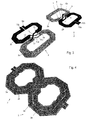
Figure 1 shows a perspective view of the layout of the primary and secondary coils of the integrated transformer; -
Figure 2 shows a sectional side view through the substrate in which the coils ofFigure 1 are formed; -
Figure 3 shows the primary coil separated from the secondary coil; -
Figure 4 shows a perspective view of the layout of the primary and secondary coils of a second embodiment of the integrated transformer; -
Figure 5 shows a top view of the primary coil separated from the secondary coil of the integrated transformer ofFigure 4 ; and -
Figure 6 shows a bottom view of the primary coil separated from the secondary coil of the integrated transformer ofFigure 4 . -
Figure 1 shows an embodiment of a layout of an integratedtransformer 1. Thetransformer 1 is for fabrication in a substrate 20 (such as silicon or GaAs) of an integrated circuit and thus comprises an on-chip monolithic transformer. The integrated circuit may solely contain thetransformer 1 or it may be integrated with other components. Thetransformer 1 is particularly suited for RF and millimetre wave applications, such as in high performance local oscillators and filters. - The integrated
transformer 1 comprises aprimary coil 2 and asecondary coil 3. The primary and secondary coils are configured, as is conventional, to transfer energy between them by inductive coupling. Theprimary coil 2 comprises afirst subsection 2a and asecond subsection 2b. Thefirst subsection 2a extends in a first plane A and the second subsection extends in a second plane B (as shown inFigure 2 ). The first plane or "upper plane" comprises, in this embodiment, an upper metal layer in thesubstrate 20 while the second plane or "lower plane", in this embodiment, comprises a metal layer lower in the substrate than the upper plane B. Thus, thesubsections - Likewise, the
secondary coil 3 comprises afirst subsection 3a and asecond subsection 3b. Thefirst subsection 3a extends in the first plane A and thesecond subsection 3b extends in the second plane B. Thus, thesubsections - The
first subsection 2a of theprimary coil 2 is stacked on top of thesecond subsection 3b of thesecondary coil 3. Further, thefirst subsection 3a of thesecondary coil 3 is stacked on top of thesecond subsection 2b of theprimary coil 2. The connections between thesubsections coils interconnect region 21. - The first and
second coils subsection subsections coils silicon substrate 20. The conductive track forms a first loop by way of the first subsection and a second loop, turning in the opposite direction, by way of the second subsection. -
Figure 3 shows theprimary coil 2 andsecondary coil 3 arranged side by side for clarity. - Referring first to the
primary coil 2, thefirst subsection 2a includes two connecting ends; a first connectingend 4 and a secondconnecting end 5. The connecting ends are formed by a break in the conductive track of the first subsection. The firstconnecting end 4 includes twoconnector fingers end 4 in the upper plane. The secondconnecting end 5 does not include a connector finger. Thesecond subsection 2b also includes two connecting ends; a first connectingend 7 and a second connecting 8. The firstconnecting end 7 includes a single connector finger 9 extending therefrom in the same, lower plane B as thesecond section 2b. - The two
connector fingers fingers end 4 of thefirst subsection 2a and an upper surface of the second connecting end 8 of thesecond subsection 2b. The vias transverse the gap between the upper plane A and the lower plane B. - The connector finger 9 includes a via (not visible) at its distal end to form an interconnection between the finger 9 of the first connecting
end 7 of thesecond subsection 2b and a lower surface of the second connectingend 5 of thefirst subsection 2a. The via transverses the gap between the lower plane B and the upper plane A. Thus, thefingers interconnect region 21. Thefingers - The
first subsection 2a includes twocoil terminals primary coil 2 to other components. A current entering the terminal 10a must follow the figure of eight path before reaching the terminal 10b. - Turning now to the
secondary coil 3, thefirst subsection 3a includes two connecting ends; a first connectingend 11 and a second connectingend 12. The connecting ends are formed by a break in the conductive track of thefirst subsection 3a. The first connectingend 11 includes asingle connector finger 13 extending therefrom theend 11 in the upper plane. The second connectingend 12 does not include a connector finger. Thesecond subsection 3b also includes two connecting ends; a first connectingend 14 and a second connecting 17. The first connectingend 14 includes twoconnector fingers second section 3b. - The
connector finger 13 includes a via (not visible) at its distal end to form an interconnection between thefinger 13 of the first connectingend 11 of thefirst subsection 3a and an upper surface of the second connectingend 17 of thesecond subsection 3b. The vias transverse the gap between the upper plane A and the lower plane B. - The
connector fingers fingers end 14 of thesecond subsection 3b and a lower surface of the second connectingend 12 of thefirst subsection 3a. The vias transverses the gap between the lower plane B and the upper plane A. Thus, thefingers finger 13 in the upper layer in theinterconnect region 21. Thefingers finger 13 as they cross. The fingers thus allow the conductive tracks to cross without an electrical interconnection between the primary and secondary coils. Thefirst subsection 3a includes twocoil terminals -
Figure 1 shows the primary coil and secondary coil arranged together wherein the primary andsecondary coils - The
fingers first subsection 2a of theprimary coil 2 are interleaved with thefinger 13 of thefirst subsection 3a of thesecondary coil 3. Thefingers fingers first subsection 2a allows thefinger 13 to extend in the gap between thefingers - The
fingers second subsection 3b of thesecondary coil 3 are interleaved with the finger 9 of thesecond subsection 2b of theprimary coil 2. Thefingers coils fingers second subsection 3b allows the finger 9 to extend in the gap between thefingers - It will be appreciated that further fingers may be provided. For example, each of the connecting ends may include two spaced fingers, the fingers configured to be interleaved over the
interconnection region 21. Alternatively, two fingers on one of the connecting ends of the primary coil may be interleaved with three fingers on the opposing connecting end of the secondary coil. - In summary, the first and second subsections of each coil are connected together by fingers that extend in the same plane as the subsection from which they project and include vias to transition between the planes. Further, the fingers of the primary coil and the fingers of the secondary coil are arranged such that they are interleaved in the plane in which they extend, thus extending side by side. This arrangement provides an efficient use of die area in the interconnect region to connect the subsections together. The fingers provide the part of the conductive track that allows the primary coil and secondary coil to overlap one another before the vias at the ends of the fingers provide the interconnection between the planes A and B.
- The invention provides a high level of integration, a symmetrical response of transformer which is advantageous for Local Oscillator and a good quality-factor and device footprint. It has also been found that this design has better immunity to pulling from adjacent blocks.
-
Figures 4 to 6 show a second embodiment of the integrated transformer in which the primary coil includes two turns and the secondary coil includes two turns. In this embodiment the first subsection of the primary coil includes an outer turn 2ao and an inner turn 2ai. The second subsection of the primary coil includes a first turn 2bf and a second turn 2bs. The inner and outer turns and the first and second turns extend in the same plane as the subsection of which they form part. Likewise, the first subsection of the secondary coil includes an outer turn 3ao and an inner turn 3ai. The second subsection of the secondary coil also a first turn 3bf and a second turn 3bs. The inner and outer turns and the first and second turns extend in the same plane as the subsection of which they form part. - The outer turn 2ao of the first subsection extends in a first, upper plane. This outer turn 2ao connects to the first turn 2bf of the second subsection, which lies in a second, intermediate plane. The first turn 2bf crosses over the second turn 2bs at a cross over region 40, opposite the
interconnect region 21. The other end of the first turn 2bf connects to the inner turn 2ai of the first subsection. The other end of the inner turn 2ai connects to the second turn of the second subsection. The second turn 2bs crosses the first turn 2bi at the cross over region 40. The second turn 2bs includes abridge section 41 to enable it to cross the first turn 2bf. Thebridge section 41 extends in a third, lower plane. Thus, this embodiment of a two turn integrated transformer extends over three distinct planes. The second turn 2bs, after thebridge section 41, connects to the outer turn 2ao of the first subsection to complete theprimary coil 2. The connections between the various turns is achieved by fingers, as in the previous embodiment, in theinterconnect region 21 between the first and second subsections. - The
secondary coil 3 has a similar construction to theprimary coil 2 in terms of the connections between the outer turn 3ao and the first turn 3bf, the first turn 3bf and the inner turn 3ai, the inner turn 3ai and the second turn 3bs, afurther bridge section 42 located in the third plane, and the connection between the second turn 3bs and the outer turn 3ao. - The primary and
secondary coils bridge sections
Claims (15)
- An integrated transformer comprising a primary coil and a secondary coil, the primary coil comprising a first subsection and a second subsection, the first subsection extending in a different plane to a plane in which the second subsection extends, the planes spaced from one another,
the secondary coil comprising a first subsection and a second subsection, the first subsection extending in a different plane to a plane in which the second subsection extends, the planes spaced from one another,
wherein the first subsection of the primary coil is stacked with the second subsection of the secondary coil and the second subsection of the primary coil is stacked with the first subsection of the secondary coil. - An integrated transformer as defined in claim 1, in which the first subsection of each coil extends in an upper plane and the second subsection of each coil extends in a lower plane.
- An integrated transformer as defined in claim 1 or claim 2, in which the first subsection of each coil is arranged in a loop.
- An integrated transformer as defined in any preceding claim, in which the second subsection of each coil is arranged in a loop.
- An integrated transformer as defined in any preceding claim, in which the first and second subsections of the primary coil and the first and second subsections of the secondary coil are each arranged in a figure of eight configuration.
- An integrated transformer as defined in any preceding claim, in which the first subsection and second subsection of the primary coil and the first subsection and the second subsection of the secondary coil are each substantially octagonal.
- An integrated transformer as defined in any preceding claim, in which the first subsection of the first subsection and second subsection of the primary coil and the first subsection and the second subsection of the secondary coil are each substantially oval or square.
- An integrated transformer as defined in any preceding claim, in which, for both of the primary and secondary coils, the first subsection includes two connecting ends for connecting to two corresponding connecting ends of the second subsection of the same coil, the connecting ends connected, between the different planes in which the subsections lie, by connector fingers.
- An integrated transformer as defined in claim 8, in which the connector fingers are narrower than a conductive track from which they extend, the primary and secondary coils formed from said conductive track.
- An integrated transformer as defined in claim 8 or claim 9, in which the connector fingers extend in same plane as the subsection from which they extend and include a via at their end to traverse the different planes to connect to the connecting end of the other subsection.
- An integrated transformer as defined in claim 9, in which, for both the primary and secondary coils, one of the connecting ends of the first subsection includes a first connector finger and one of the connector ends of the second subsection of the same coil includes a second connector finger, the first and second connector fingers arranged to cross over one another in the different planes in an interconnection region.
- An integrated transformer as defined in claims 11, in which the connector finger of the first subsection of the primary coil is interleaved with and extends in the same plane as the connector finger of the first subsection of the secondary coil; and
the connector finger of the second subsection of the primary coil is interleaved with and extends in the same plane as the connector finger of the second subsection of the secondary coil. - An integrated transformer as defined in claim 2, in which the first subsection of each of the primary and secondary coils includes coil terminals for providing a connection to the coils.
- An oscillator including the integrated transformer as defined in any one of claims 1 to 13.
- An integrated circuit for a RF device including the integrated transformer of any one of claims 1 to 14.
Priority Applications (3)
| Application Number | Priority Date | Filing Date | Title |
|---|---|---|---|
| EP13290318.8A EP2887364B1 (en) | 2013-12-18 | 2013-12-18 | Integrated transformer |
| CN201410685834.0A CN104733429B (en) | 2013-12-18 | 2014-11-25 | Integrated transformer |
| US14/573,630 US9305697B2 (en) | 2013-12-18 | 2014-12-17 | Integrated transformer |
Applications Claiming Priority (1)
| Application Number | Priority Date | Filing Date | Title |
|---|---|---|---|
| EP13290318.8A EP2887364B1 (en) | 2013-12-18 | 2013-12-18 | Integrated transformer |
Publications (2)
| Publication Number | Publication Date |
|---|---|
| EP2887364A1 true EP2887364A1 (en) | 2015-06-24 |
| EP2887364B1 EP2887364B1 (en) | 2017-06-07 |
Family
ID=50023394
Family Applications (1)
| Application Number | Title | Priority Date | Filing Date |
|---|---|---|---|
| EP13290318.8A Active EP2887364B1 (en) | 2013-12-18 | 2013-12-18 | Integrated transformer |
Country Status (3)
| Country | Link |
|---|---|
| US (1) | US9305697B2 (en) |
| EP (1) | EP2887364B1 (en) |
| CN (1) | CN104733429B (en) |
Families Citing this family (25)
| Publication number | Priority date | Publication date | Assignee | Title |
|---|---|---|---|---|
| CN106972009B (en) * | 2016-01-13 | 2020-06-12 | 瑞昱半导体股份有限公司 | Integrated inductor structure |
| JP6551256B2 (en) * | 2016-02-17 | 2019-07-31 | Tdk株式会社 | Coil component, circuit board incorporating coil component, and power supply circuit including coil component |
| CN107437456B (en) * | 2016-05-25 | 2021-03-23 | 台达电子企业管理(上海)有限公司 | Magnetic core structure and magnetic element |
| US11728087B2 (en) | 2016-05-25 | 2023-08-15 | Delta Electronics (Shanghai) Co., Ltd | Core structure and magnetic device |
| US10418172B2 (en) * | 2016-12-07 | 2019-09-17 | Astec International Limited | Methods of forming coils for inductive components |
| US10367452B2 (en) * | 2017-03-16 | 2019-07-30 | Infineon Technologies Ag | System and method for a dual-core VCO |
| TWI598899B (en) * | 2017-05-11 | 2017-09-11 | 瑞昱半導體股份有限公司 | Inductor device |
| US11283296B2 (en) * | 2017-05-26 | 2022-03-22 | Nucurrent, Inc. | Crossover inductor coil and assembly for wireless transmission |
| CN107731793B (en) * | 2017-09-14 | 2019-12-17 | 建荣半导体(深圳)有限公司 | Figure 8 inductor structure and semiconductor structure integrated on a semiconductor chip |
| TWI632661B (en) * | 2017-09-20 | 2018-08-11 | 瑞昱半導體股份有限公司 | Integral inductor device |
| TWI643216B (en) * | 2017-11-10 | 2018-12-01 | 瑞昱半導體股份有限公司 | Integrated inductor |
| CN108022914A (en) * | 2017-11-19 | 2018-05-11 | 天津大学 | A kind of Terahertz transformer realized using standard CMOS process |
| EP3712912B1 (en) * | 2017-12-27 | 2023-11-22 | Huawei Technologies Co., Ltd. | Oscillator system comprising a transformer |
| TWI659437B (en) * | 2018-06-22 | 2019-05-11 | 瑞昱半導體股份有限公司 | Transformer device |
| TWI674595B (en) * | 2019-04-25 | 2019-10-11 | 瑞昱半導體股份有限公司 | Integrated transformer |
| CN111292922B (en) * | 2020-02-17 | 2022-03-15 | 电子科技大学 | 8-shaped four-way power combiner with low insertion loss |
| TWI727815B (en) * | 2020-05-29 | 2021-05-11 | 瑞昱半導體股份有限公司 | Integrated circuit |
| US11245426B2 (en) * | 2020-06-04 | 2022-02-08 | Samsung Electronics Co., Ltd. | Band switching balun |
| US11283303B2 (en) | 2020-07-24 | 2022-03-22 | Nucurrent, Inc. | Area-apportioned wireless power antenna for maximized charging volume |
| CN112259348B (en) * | 2020-10-21 | 2022-01-11 | 清华大学 | Integrated inductive device and amplifier |
| US11695302B2 (en) | 2021-02-01 | 2023-07-04 | Nucurrent, Inc. | Segmented shielding for wide area wireless power transmitter |
| WO2023133288A1 (en) * | 2022-01-07 | 2023-07-13 | Sehat Sutardja | Offset transformer structure |
| TWI792936B (en) | 2022-03-07 | 2023-02-11 | 瑞昱半導體股份有限公司 | Inductor device |
| CN116798748A (en) * | 2022-03-15 | 2023-09-22 | 瑞昱半导体股份有限公司 | Inductive device |
| US20240321730A1 (en) * | 2023-03-24 | 2024-09-26 | Qualcomm Incorporated | Integrated device comprising stacked inductors with low or no mutual inductance |
Citations (4)
| Publication number | Priority date | Publication date | Assignee | Title |
|---|---|---|---|---|
| US20090284339A1 (en) * | 2008-05-14 | 2009-11-19 | Samsung Electronics Co., Ltd. | Transformers, balanced-unbalanced transformers (baluns) and Integrated circuits including the same |
| US20120319779A1 (en) * | 2011-06-17 | 2012-12-20 | Youn Suk Kim | Transformer and cmos power amplifier including the same |
| US20130154783A1 (en) * | 2011-12-19 | 2013-06-20 | Murata Manufacturing Co., Ltd. | High-frequency transformer, high-frequency component, and communication terminal device |
| EP2669907A1 (en) * | 2012-05-28 | 2013-12-04 | NXP Semiconductors B.V. | An integrated circuit based transformer |
Family Cites Families (8)
| Publication number | Priority date | Publication date | Assignee | Title |
|---|---|---|---|---|
| DE10233980A1 (en) | 2002-07-25 | 2004-02-12 | Philips Intellectual Property & Standards Gmbh | planar inductor |
| US6967555B2 (en) * | 2002-10-17 | 2005-11-22 | Via Technologies Inc. | Multi-level symmetrical inductor |
| US7151430B2 (en) | 2004-03-03 | 2006-12-19 | Telefonaktiebolaget Lm Ericsson (Publ) | Method of and inductor layout for reduced VCO coupling |
| TWI238515B (en) * | 2004-10-08 | 2005-08-21 | Winbond Electronics Corp | Integrated transformer with stack structure |
| KR100777394B1 (en) * | 2006-05-17 | 2007-11-19 | 삼성전자주식회사 | On-chip transformer baluns to improve amplitude imbalance |
| EP2281292B1 (en) * | 2008-05-29 | 2016-08-10 | ST-Ericsson SA | Radio frequency eight-shaped balun |
| KR101904364B1 (en) * | 2010-12-23 | 2018-11-30 | 마벨 월드 트레이드 리미티드 | Figure 8 balun |
| US9312060B2 (en) * | 2012-09-20 | 2016-04-12 | Marvell World Trade Ltd. | Transformer circuits having transformers with figure eight and double figure eight nested structures |
-
2013
- 2013-12-18 EP EP13290318.8A patent/EP2887364B1/en active Active
-
2014
- 2014-11-25 CN CN201410685834.0A patent/CN104733429B/en active Active
- 2014-12-17 US US14/573,630 patent/US9305697B2/en active Active
Patent Citations (4)
| Publication number | Priority date | Publication date | Assignee | Title |
|---|---|---|---|---|
| US20090284339A1 (en) * | 2008-05-14 | 2009-11-19 | Samsung Electronics Co., Ltd. | Transformers, balanced-unbalanced transformers (baluns) and Integrated circuits including the same |
| US20120319779A1 (en) * | 2011-06-17 | 2012-12-20 | Youn Suk Kim | Transformer and cmos power amplifier including the same |
| US20130154783A1 (en) * | 2011-12-19 | 2013-06-20 | Murata Manufacturing Co., Ltd. | High-frequency transformer, high-frequency component, and communication terminal device |
| EP2669907A1 (en) * | 2012-05-28 | 2013-12-04 | NXP Semiconductors B.V. | An integrated circuit based transformer |
Also Published As
| Publication number | Publication date |
|---|---|
| CN104733429A (en) | 2015-06-24 |
| US9305697B2 (en) | 2016-04-05 |
| CN104733429B (en) | 2017-12-19 |
| US20150170824A1 (en) | 2015-06-18 |
| EP2887364B1 (en) | 2017-06-07 |
Similar Documents
| Publication | Publication Date | Title |
|---|---|---|
| EP2887364B1 (en) | Integrated transformer | |
| KR100349419B1 (en) | Dual-layer spiral inductor | |
| KR101453071B1 (en) | Transformer balun and integrated circuit including the same | |
| CN102468035B (en) | Balun system and method | |
| JP4766354B1 (en) | Multilayer bandpass filter | |
| US6380608B1 (en) | Multiple level spiral inductors used to form a filter in a printed circuit board | |
| US9773606B2 (en) | Integrated stacked transformer | |
| US9330832B2 (en) | Integrated transformer balun with enhanced common-mode rejection for radio frequency, microwave, and millimeter-wave integrated circuits | |
| TWI584584B (en) | High frequency component and filter component | |
| TWI565227B (en) | Broadband integrated rf/microwave/millimeter mixer with integrated balun(s) | |
| US20070126544A1 (en) | Inductive component | |
| JP2003087008A (en) | Multilayer dielectric filter | |
| US9698831B2 (en) | Transformer and communication terminal device | |
| US8212630B2 (en) | Thin film balun | |
| CN107431468B (en) | electronic components | |
| JP5051062B2 (en) | Thin film balun | |
| US20060055495A1 (en) | Planar transformer | |
| US8203396B2 (en) | Thin film balun | |
| CN103400820B (en) | Semiconductor device | |
| JP2006066769A (en) | Inductor and manufacturing method thereof | |
| JP2006270444A (en) | Unbalanced to balanced converter | |
| EP2669907A1 (en) | An integrated circuit based transformer | |
| JP2002050740A (en) | Spiral inductor | |
| JP4457362B2 (en) | Electronic components | |
| JP7430376B2 (en) | Spiral inductors and passive integrated circuits |
Legal Events
| Date | Code | Title | Description |
|---|---|---|---|
| PUAI | Public reference made under article 153(3) epc to a published international application that has entered the european phase |
Free format text: ORIGINAL CODE: 0009012 |
|
| 17P | Request for examination filed |
Effective date: 20140327 |
|
| AK | Designated contracting states |
Kind code of ref document: A1 Designated state(s): AL AT BE BG CH CY CZ DE DK EE ES FI FR GB GR HR HU IE IS IT LI LT LU LV MC MK MT NL NO PL PT RO RS SE SI SK SM TR |
|
| AX | Request for extension of the european patent |
Extension state: BA ME |
|
| RBV | Designated contracting states (corrected) |
Designated state(s): AL AT BE BG CH CY CZ DE DK EE ES FI FR GB GR HR HU IE IS IT LI LT LU LV MC MK MT NL NO PL PT RO RS SE SI SK SM TR |
|
| GRAP | Despatch of communication of intention to grant a patent |
Free format text: ORIGINAL CODE: EPIDOSNIGR1 |
|
| RIC1 | Information provided on ipc code assigned before grant |
Ipc: H01F 17/00 20060101AFI20160912BHEP Ipc: H01F 27/28 20060101ALI20160912BHEP |
|
| INTG | Intention to grant announced |
Effective date: 20161013 |
|
| GRAJ | Information related to disapproval of communication of intention to grant by the applicant or resumption of examination proceedings by the epo deleted |
Free format text: ORIGINAL CODE: EPIDOSDIGR1 |
|
| STAA | Information on the status of an ep patent application or granted ep patent |
Free format text: STATUS: REQUEST FOR EXAMINATION WAS MADE |
|
| INTC | Intention to grant announced (deleted) | ||
| GRAP | Despatch of communication of intention to grant a patent |
Free format text: ORIGINAL CODE: EPIDOSNIGR1 |
|
| STAA | Information on the status of an ep patent application or granted ep patent |
Free format text: STATUS: GRANT OF PATENT IS INTENDED |
|
| INTG | Intention to grant announced |
Effective date: 20170103 |
|
| GRAS | Grant fee paid |
Free format text: ORIGINAL CODE: EPIDOSNIGR3 |
|
| AK | Designated contracting states |
Kind code of ref document: B1 Designated state(s): AL AT BE BG CH CY CZ DE DK EE ES FI FR GB GR HR HU IE IS IT LI LT LU LV MC MK MT NL NO PL PT RO RS SE SI SK SM TR |
|
| REG | Reference to a national code |
Ref country code: GB Ref legal event code: FG4D |
|
| GRAA | (expected) grant |
Free format text: ORIGINAL CODE: 0009210 |
|
| REG | Reference to a national code |
Ref country code: CH Ref legal event code: EP Ref country code: AT Ref legal event code: REF Ref document number: 899762 Country of ref document: AT Kind code of ref document: T Effective date: 20170615 |
|
| STAA | Information on the status of an ep patent application or granted ep patent |
Free format text: STATUS: THE PATENT HAS BEEN GRANTED |
|
| REG | Reference to a national code |
Ref country code: IE Ref legal event code: FG4D |
|
| REG | Reference to a national code |
Ref country code: DE Ref legal event code: R096 Ref document number: 602013021927 Country of ref document: DE |
|
| REG | Reference to a national code |
Ref country code: NL Ref legal event code: MP Effective date: 20170607 |
|
| REG | Reference to a national code |
Ref country code: LT Ref legal event code: MG4D |
|
| PG25 | Lapsed in a contracting state [announced via postgrant information from national office to epo] |
Ref country code: GR Free format text: LAPSE BECAUSE OF FAILURE TO SUBMIT A TRANSLATION OF THE DESCRIPTION OR TO PAY THE FEE WITHIN THE PRESCRIBED TIME-LIMIT Effective date: 20170908 Ref country code: NO Free format text: LAPSE BECAUSE OF FAILURE TO SUBMIT A TRANSLATION OF THE DESCRIPTION OR TO PAY THE FEE WITHIN THE PRESCRIBED TIME-LIMIT Effective date: 20170907 Ref country code: FI Free format text: LAPSE BECAUSE OF FAILURE TO SUBMIT A TRANSLATION OF THE DESCRIPTION OR TO PAY THE FEE WITHIN THE PRESCRIBED TIME-LIMIT Effective date: 20170607 Ref country code: ES Free format text: LAPSE BECAUSE OF FAILURE TO SUBMIT A TRANSLATION OF THE DESCRIPTION OR TO PAY THE FEE WITHIN THE PRESCRIBED TIME-LIMIT Effective date: 20170607 Ref country code: LT Free format text: LAPSE BECAUSE OF FAILURE TO SUBMIT A TRANSLATION OF THE DESCRIPTION OR TO PAY THE FEE WITHIN THE PRESCRIBED TIME-LIMIT Effective date: 20170607 Ref country code: HR Free format text: LAPSE BECAUSE OF FAILURE TO SUBMIT A TRANSLATION OF THE DESCRIPTION OR TO PAY THE FEE WITHIN THE PRESCRIBED TIME-LIMIT Effective date: 20170607 |
|
| REG | Reference to a national code |
Ref country code: AT Ref legal event code: MK05 Ref document number: 899762 Country of ref document: AT Kind code of ref document: T Effective date: 20170607 |
|
| REG | Reference to a national code |
Ref country code: FR Ref legal event code: PLFP Year of fee payment: 5 |
|
| PG25 | Lapsed in a contracting state [announced via postgrant information from national office to epo] |
Ref country code: LV Free format text: LAPSE BECAUSE OF FAILURE TO SUBMIT A TRANSLATION OF THE DESCRIPTION OR TO PAY THE FEE WITHIN THE PRESCRIBED TIME-LIMIT Effective date: 20170607 Ref country code: NL Free format text: LAPSE BECAUSE OF FAILURE TO SUBMIT A TRANSLATION OF THE DESCRIPTION OR TO PAY THE FEE WITHIN THE PRESCRIBED TIME-LIMIT Effective date: 20170607 Ref country code: RS Free format text: LAPSE BECAUSE OF FAILURE TO SUBMIT A TRANSLATION OF THE DESCRIPTION OR TO PAY THE FEE WITHIN THE PRESCRIBED TIME-LIMIT Effective date: 20170607 Ref country code: BG Free format text: LAPSE BECAUSE OF FAILURE TO SUBMIT A TRANSLATION OF THE DESCRIPTION OR TO PAY THE FEE WITHIN THE PRESCRIBED TIME-LIMIT Effective date: 20170907 Ref country code: SE Free format text: LAPSE BECAUSE OF FAILURE TO SUBMIT A TRANSLATION OF THE DESCRIPTION OR TO PAY THE FEE WITHIN THE PRESCRIBED TIME-LIMIT Effective date: 20170607 |
|
| PG25 | Lapsed in a contracting state [announced via postgrant information from national office to epo] |
Ref country code: RO Free format text: LAPSE BECAUSE OF FAILURE TO SUBMIT A TRANSLATION OF THE DESCRIPTION OR TO PAY THE FEE WITHIN THE PRESCRIBED TIME-LIMIT Effective date: 20170607 Ref country code: AT Free format text: LAPSE BECAUSE OF FAILURE TO SUBMIT A TRANSLATION OF THE DESCRIPTION OR TO PAY THE FEE WITHIN THE PRESCRIBED TIME-LIMIT Effective date: 20170607 Ref country code: SK Free format text: LAPSE BECAUSE OF FAILURE TO SUBMIT A TRANSLATION OF THE DESCRIPTION OR TO PAY THE FEE WITHIN THE PRESCRIBED TIME-LIMIT Effective date: 20170607 Ref country code: CZ Free format text: LAPSE BECAUSE OF FAILURE TO SUBMIT A TRANSLATION OF THE DESCRIPTION OR TO PAY THE FEE WITHIN THE PRESCRIBED TIME-LIMIT Effective date: 20170607 Ref country code: EE Free format text: LAPSE BECAUSE OF FAILURE TO SUBMIT A TRANSLATION OF THE DESCRIPTION OR TO PAY THE FEE WITHIN THE PRESCRIBED TIME-LIMIT Effective date: 20170607 |
|
| PG25 | Lapsed in a contracting state [announced via postgrant information from national office to epo] |
Ref country code: PL Free format text: LAPSE BECAUSE OF FAILURE TO SUBMIT A TRANSLATION OF THE DESCRIPTION OR TO PAY THE FEE WITHIN THE PRESCRIBED TIME-LIMIT Effective date: 20170607 Ref country code: SM Free format text: LAPSE BECAUSE OF FAILURE TO SUBMIT A TRANSLATION OF THE DESCRIPTION OR TO PAY THE FEE WITHIN THE PRESCRIBED TIME-LIMIT Effective date: 20170607 Ref country code: IS Free format text: LAPSE BECAUSE OF FAILURE TO SUBMIT A TRANSLATION OF THE DESCRIPTION OR TO PAY THE FEE WITHIN THE PRESCRIBED TIME-LIMIT Effective date: 20171007 Ref country code: IT Free format text: LAPSE BECAUSE OF FAILURE TO SUBMIT A TRANSLATION OF THE DESCRIPTION OR TO PAY THE FEE WITHIN THE PRESCRIBED TIME-LIMIT Effective date: 20170607 |
|
| REG | Reference to a national code |
Ref country code: DE Ref legal event code: R097 Ref document number: 602013021927 Country of ref document: DE |
|
| PLBE | No opposition filed within time limit |
Free format text: ORIGINAL CODE: 0009261 |
|
| STAA | Information on the status of an ep patent application or granted ep patent |
Free format text: STATUS: NO OPPOSITION FILED WITHIN TIME LIMIT |
|
| PG25 | Lapsed in a contracting state [announced via postgrant information from national office to epo] |
Ref country code: DK Free format text: LAPSE BECAUSE OF FAILURE TO SUBMIT A TRANSLATION OF THE DESCRIPTION OR TO PAY THE FEE WITHIN THE PRESCRIBED TIME-LIMIT Effective date: 20170607 |
|
| 26N | No opposition filed |
Effective date: 20180308 |
|
| PG25 | Lapsed in a contracting state [announced via postgrant information from national office to epo] |
Ref country code: SI Free format text: LAPSE BECAUSE OF FAILURE TO SUBMIT A TRANSLATION OF THE DESCRIPTION OR TO PAY THE FEE WITHIN THE PRESCRIBED TIME-LIMIT Effective date: 20170607 |
|
| REG | Reference to a national code |
Ref country code: CH Ref legal event code: PL |
|
| GBPC | Gb: european patent ceased through non-payment of renewal fee |
Effective date: 20171218 |
|
| REG | Reference to a national code |
Ref country code: IE Ref legal event code: MM4A |
|
| PG25 | Lapsed in a contracting state [announced via postgrant information from national office to epo] |
Ref country code: MT Free format text: LAPSE BECAUSE OF NON-PAYMENT OF DUE FEES Effective date: 20171218 Ref country code: LU Free format text: LAPSE BECAUSE OF NON-PAYMENT OF DUE FEES Effective date: 20171218 |
|
| REG | Reference to a national code |
Ref country code: BE Ref legal event code: MM Effective date: 20171231 |
|
| PG25 | Lapsed in a contracting state [announced via postgrant information from national office to epo] |
Ref country code: IE Free format text: LAPSE BECAUSE OF NON-PAYMENT OF DUE FEES Effective date: 20171218 |
|
| PG25 | Lapsed in a contracting state [announced via postgrant information from national office to epo] |
Ref country code: LI Free format text: LAPSE BECAUSE OF NON-PAYMENT OF DUE FEES Effective date: 20171231 Ref country code: CH Free format text: LAPSE BECAUSE OF NON-PAYMENT OF DUE FEES Effective date: 20171231 Ref country code: BE Free format text: LAPSE BECAUSE OF NON-PAYMENT OF DUE FEES Effective date: 20171231 Ref country code: GB Free format text: LAPSE BECAUSE OF NON-PAYMENT OF DUE FEES Effective date: 20171218 |
|
| PG25 | Lapsed in a contracting state [announced via postgrant information from national office to epo] |
Ref country code: MC Free format text: LAPSE BECAUSE OF FAILURE TO SUBMIT A TRANSLATION OF THE DESCRIPTION OR TO PAY THE FEE WITHIN THE PRESCRIBED TIME-LIMIT Effective date: 20170607 Ref country code: HU Free format text: LAPSE BECAUSE OF FAILURE TO SUBMIT A TRANSLATION OF THE DESCRIPTION OR TO PAY THE FEE WITHIN THE PRESCRIBED TIME-LIMIT; INVALID AB INITIO Effective date: 20131218 |
|
| PG25 | Lapsed in a contracting state [announced via postgrant information from national office to epo] |
Ref country code: CY Free format text: LAPSE BECAUSE OF FAILURE TO SUBMIT A TRANSLATION OF THE DESCRIPTION OR TO PAY THE FEE WITHIN THE PRESCRIBED TIME-LIMIT Effective date: 20170607 |
|
| PG25 | Lapsed in a contracting state [announced via postgrant information from national office to epo] |
Ref country code: MK Free format text: LAPSE BECAUSE OF FAILURE TO SUBMIT A TRANSLATION OF THE DESCRIPTION OR TO PAY THE FEE WITHIN THE PRESCRIBED TIME-LIMIT Effective date: 20170607 |
|
| PG25 | Lapsed in a contracting state [announced via postgrant information from national office to epo] |
Ref country code: TR Free format text: LAPSE BECAUSE OF FAILURE TO SUBMIT A TRANSLATION OF THE DESCRIPTION OR TO PAY THE FEE WITHIN THE PRESCRIBED TIME-LIMIT Effective date: 20170607 |
|
| PG25 | Lapsed in a contracting state [announced via postgrant information from national office to epo] |
Ref country code: PT Free format text: LAPSE BECAUSE OF FAILURE TO SUBMIT A TRANSLATION OF THE DESCRIPTION OR TO PAY THE FEE WITHIN THE PRESCRIBED TIME-LIMIT Effective date: 20170607 |
|
| PG25 | Lapsed in a contracting state [announced via postgrant information from national office to epo] |
Ref country code: AL Free format text: LAPSE BECAUSE OF FAILURE TO SUBMIT A TRANSLATION OF THE DESCRIPTION OR TO PAY THE FEE WITHIN THE PRESCRIBED TIME-LIMIT Effective date: 20170607 |
|
| P01 | Opt-out of the competence of the unified patent court (upc) registered |
Effective date: 20230725 |
|
| PGFP | Annual fee paid to national office [announced via postgrant information from national office to epo] |
Ref country code: DE Payment date: 20251126 Year of fee payment: 13 |
|
| PGFP | Annual fee paid to national office [announced via postgrant information from national office to epo] |
Ref country code: FR Payment date: 20251120 Year of fee payment: 13 |