EP2884676B1 - Small base station for mobile communication system - Google Patents
Small base station for mobile communication system Download PDFInfo
- Publication number
- EP2884676B1 EP2884676B1 EP13828208.2A EP13828208A EP2884676B1 EP 2884676 B1 EP2884676 B1 EP 2884676B1 EP 13828208 A EP13828208 A EP 13828208A EP 2884676 B1 EP2884676 B1 EP 2884676B1
- Authority
- EP
- European Patent Office
- Prior art keywords
- base station
- outer surfaces
- box
- disposed
- boards
- Prior art date
- Legal status (The legal status is an assumption and is not a legal conclusion. Google has not performed a legal analysis and makes no representation as to the accuracy of the status listed.)
- Active
Links
- 238000010295 mobile communication Methods 0.000 title claims description 8
- 230000005540 biological transmission Effects 0.000 claims description 2
- 230000005855 radiation Effects 0.000 description 10
- 238000004891 communication Methods 0.000 description 3
- 238000001816 cooling Methods 0.000 description 2
- RKTYLMNFRDHKIL-UHFFFAOYSA-N copper;5,10,15,20-tetraphenylporphyrin-22,24-diide Chemical compound [Cu+2].C1=CC(C(=C2C=CC([N-]2)=C(C=2C=CC=CC=2)C=2C=CC(N=2)=C(C=2C=CC=CC=2)C2=CC=C3[N-]2)C=2C=CC=CC=2)=NC1=C3C1=CC=CC=C1 RKTYLMNFRDHKIL-UHFFFAOYSA-N 0.000 description 2
- 230000001419 dependent effect Effects 0.000 description 1
- 230000000694 effects Effects 0.000 description 1
- 238000012544 monitoring process Methods 0.000 description 1
- 230000002093 peripheral effect Effects 0.000 description 1
- 230000008054 signal transmission Effects 0.000 description 1
Images


Classifications
-
- H—ELECTRICITY
- H04—ELECTRIC COMMUNICATION TECHNIQUE
- H04B—TRANSMISSION
- H04B7/00—Radio transmission systems, i.e. using radiation field
- H04B7/14—Relay systems
- H04B7/15—Active relay systems
- H04B7/155—Ground-based stations
-
- H—ELECTRICITY
- H04—ELECTRIC COMMUNICATION TECHNIQUE
- H04W—WIRELESS COMMUNICATION NETWORKS
- H04W88/00—Devices specially adapted for wireless communication networks, e.g. terminals, base stations or access point devices
- H04W88/08—Access point devices
-
- H—ELECTRICITY
- H01—ELECTRIC ELEMENTS
- H01Q—ANTENNAS, i.e. RADIO AERIALS
- H01Q1/00—Details of, or arrangements associated with, antennas
- H01Q1/02—Arrangements for de-icing; Arrangements for drying-out ; Arrangements for cooling; Arrangements for preventing corrosion
-
- H—ELECTRICITY
- H01—ELECTRIC ELEMENTS
- H01Q—ANTENNAS, i.e. RADIO AERIALS
- H01Q1/00—Details of, or arrangements associated with, antennas
- H01Q1/12—Supports; Mounting means
- H01Q1/22—Supports; Mounting means by structural association with other equipment or articles
- H01Q1/24—Supports; Mounting means by structural association with other equipment or articles with receiving set
- H01Q1/241—Supports; Mounting means by structural association with other equipment or articles with receiving set used in mobile communications, e.g. GSM
- H01Q1/246—Supports; Mounting means by structural association with other equipment or articles with receiving set used in mobile communications, e.g. GSM specially adapted for base stations
-
- H—ELECTRICITY
- H01—ELECTRIC ELEMENTS
- H01Q—ANTENNAS, i.e. RADIO AERIALS
- H01Q15/00—Devices for reflection, refraction, diffraction or polarisation of waves radiated from an antenna, e.g. quasi-optical devices
- H01Q15/14—Reflecting surfaces; Equivalent structures
-
- H—ELECTRICITY
- H01—ELECTRIC ELEMENTS
- H01Q—ANTENNAS, i.e. RADIO AERIALS
- H01Q21/00—Antenna arrays or systems
- H01Q21/24—Combinations of antenna units polarised in different directions for transmitting or receiving circularly and elliptically polarised waves or waves linearly polarised in any direction
- H01Q21/26—Turnstile or like antennas comprising arrangements of three or more elongated elements disposed radially and symmetrically in a horizontal plane about a common centre
-
- H—ELECTRICITY
- H04—ELECTRIC COMMUNICATION TECHNIQUE
- H04Q—SELECTING
- H04Q1/00—Details of selecting apparatus or arrangements
- H04Q1/02—Constructional details
- H04Q1/025—Cabinets
Definitions
- the present invention relates to a base station of a mobile communication system, and more particularly to a small base station installed in a building or a house.
- a base station of a mobile communication system refers to a system for relaying electric waves of a portable terminal in a cell.
- the base station is generally installed on a roof of a building to relay electric waves of a portable terminal. Accordingly, base stations are present in units of cells, and the base stations controls transmission of signals, designation of a communication channel, and monitoring of a communication channel in units of cells, as well as an interface function between the portable terminal and a switch center.
- the antennas employed in the base station are distributed due to presence of many control antennas which may be vertically or horizontally beam-tilted.
- a small base station for improving communication quality while reducing frequency load is installed as a system for covering an area which is still smaller than the radius of the current existing mobile communication service.
- the base station is used to accommodate data traffic intensively generated in a small area.
- a shading area can be solved and a higher network and a convergence service can be realized.
- the small base station employed in the existing mobile communication system is configured such that main components mounted to the interior of the base station, for example, a main board, a power supply unit, an antenna, and a power amplifier are vertically stacked, there is a limit in reducing the entire size of the base station.
- the small base station according to the related art is configured such that a main board, a power supply unit and the like are installed on one board, the overall size of the main board become larger and heat emission of the power amplifier becomes problematic.
- EP 2 389 710 B1 discloses an enclosing and a mounting structure for an antenna comprising a tube that has an outer surface adapted for mounting transmitter and/or receiver components thereon and an inner surface defining a cooling chimney, and a radome which has an opening at each end of the tube for allowing air to circulate through the cooling chimney.
- the chimney enhances air flow and provides improved heat removal by the airflow.
- a chimney has to be of a certain length in order to provide sufficient air flow, which does not support the desired small size.
- EP 2 408 121 A1 describes a radio frequency unit and an integrated antenna.
- the radio frequency unit includes a duplexer, a power amplifier circuit board, and a transceiver circuit board.
- the power amplifier circuit board and the transceiver circuit board are respectively located at two end portions of the duplexer.
- the power amplifier circuit board and the transceiver circuit board are projected onto the same plane along a direction being vertical to the power amplifier circuit board with their projections on the same plane non-overlapped each other.
- US 2012/014697 A1 describes an antenna device, which includes a first antenna unit and a second antenna unit.
- the first antenna unit includes a first radiation module, a power divider/combiner network connected to the first radiation module, and a feeder interface connected to the power divider/combiner network.
- the second antenna unit includes a second radiation module, a transceiver array connected to the second radiation module, a baseband processing unit.
- the present invention provides a small base station of a mobile communication system which can advantageously realize a small size by three-dimensionally disposing main elements at proper places with respect to a box.
- the present invention also provides a small base station of a mobile communication system which can minimize a heat emission problem by disposing a plurality of power amplifiers such that they are spaced apart from each other by the farthest distance.
- the digital interface module and the antenna unit are stacked in the Z axis direction, but the first and second power amplifiers, the up/down converter, and the power supply unit are disposed along the X and Y axes such that the base station can be made small.
- a plurality of boards are not vertically stacked but are three-dimensionally disposed along the outer surfaces of the box in consideration of heat emission, so that the boards can be efficiently mounted in a limited space.
- the present invention includes: a polyhedral box; an antenna unit installed on the widest one of outer surfaces of the box; a first board disposed on any one of the outer surfaces of the box; and at least two other boards disposed in an upright position from the first board.
- the Cartesian coordinate system shown in FIGS. 1 and 2 is used, in which the X axis denotes a transverse direction, the Y axis denotes a longitudinal direction, and the Z axis denotes a perpendicular direction.
- the base station 10 according to the present invention is small-sized in a transverse direction, a longitudinal direction, and a perpendicular direction thereof as compared with the related art, but maintains a performance of an existing base station despite the small size. That is, the small size means that the entire size of the base station is small long the three axes as compared with the related art.
- FIG. 1 shows an external appearance of the small base station 10 (hereinafter, simply referred to as a base station) according to the present invention.
- FIG. 1 shows an assembled state of the base station 10, and shows an external appearance of the base station 10 in which an outer cover 11 and a heat sink 12 are coupled to each other.
- the heat sink 12 is disposed on the bottom of the base station 10 to support main elements mounted on the heat sink 12, and the outer cover 11 is coupled to the heat sink in the Z axis direction to protect main internal elements.
- FIG. 2 is an exploded perspective view showing a configuration of the base station 10 according to the present invention.
- an antenna unit 15 at least three boards B1 to B4 (printed circuit boards), a power supply unit (PSU) 14, and a heat sink 12, including a box 13, are three-dimensionally disposed at proper locations of the base station 10.
- PSU power supply unit
- the three-dimensional disposition of the plurality of boards does mean that the boards are not stacked along one axis but the main elements are disposed in consideration of the three axes including the X, Y, and Z axes, and in particular means that a plurality of boards are disposed in a reference board in an upright position along the X and Y axes and the remaining main elements are disposed along the Z axis, which three-dimensional disposition is advantageous in the small-size of the base station.
- the base station 10 according to the present invention considers a heat emission problem as well as the three-dimensional disposition of the main elements.
- the box 13 has a polyhedral shape, for example, a rectangular parallelepiped shape, and includes a plurality of outer surfaces and a plurality of inner walls and the antenna unit 15 is accommodated in the interior space.
- the box 13 has an open-topped box shape, and has at least three inner walls 136, at least three outer surfaces 131 to 134, and a bottom surface 135.
- the outer surfaces of the box include at least three outer surfaces 131 to 134, and a bottom surface 135.
- the inner walls include at least three inner walls.
- FIGS. 2 and 3 show four inner walls 136, and four outer surfaces 131 to 134.
- the outer surfaces and the inner walls have the same shapes and the same sizes.
- the plurality of outer surfaces include first and second outer surfaces 131 and 132 facing each other, and third and fourth outer surfaces 133 and 134 disposed between the first and second outer surfaces 131 and 132 while facing the first and second outer surfaces 131 and 132, respectively.
- the first and second outer surfaces 131 and 132 are parallel to each other, and the third and fourth outer surfaces 133 and 134 are parallel to each other.
- the first outer surfaces 131 is perpendicular to the third and fourth surfaces 133 and 134
- the second outer surface 132 is perpendicular to the third and fourth surfaces 133 and 134.
- the first to fourth outer surfaces 131 to 134 are flat. Because the box has a rectangular parallelepiped shape, the first to fourth outer surfaces 131 to 134 have a rectangular shape.
- the box 13 has a plurality of outer surfaces, in which in the aspect of the shapes of the outer surfaces, the first outer surface 131 and the second outer surface 132 may have the same rectangular or square shape, the third outer surface 133 and the fourth outer surface 134 may have the same rectangular or square shape, and the bottom surface 135 also may have a rectangular or square shape.
- the first and second outer surfaces 131 and 132 and the third and fourth outer surfaces 133 and 134 of the box may have a rectangular shape of the same size, may have rectangular shapes of different sizes, or may have a square shape of the same size.
- the bottom surface 135 of the outer surfaces which is located at the bottom of the box, may have a rectangular or square shape, or may have a shape larger than, smaller than, or the same as those of the first and second outer surfaces 131 and 132 and the third and fourth outer surfaces 133 and 134. It is preferable that the box 13 according to the present invention has a bottom surface 135 which is wider than the first and second outer surfaces 131 and 132 and the third and fourth outer surfaces 133 and 134. FIG. 2 shows that the box 2 has a bottom surface 135 which is wider than the first and second outer surfaces 131 and 132 and the third and fourth outer surfaces 133 and 134. It is preferable that the bottom surface 135 has the widest area such that the antenna unit 15 is disposed parallel to the bottom surface 135.
- a plurality of boards B1 to B4, and the power supply unit 14 are disposed on the outer surfaces of the box 13.
- the plurality of boards includes first and fourth boards B1 to B4.
- the first board B1 is disposed on the bottom surface 135 of the box 13.
- the second and third boards B2 and B3 are disposed on the first and second outer surfaces 131 and 132 of the box 13.
- the fourth board B4 is disposed on the third outer surface 133.
- the power supply unit 14 is disposed on the fourth outer surface 134.
- the first board B1 is a digital interface module, and is disposed in parallel to the bottom surface of the box 135 while facing the bottom surface of the box 135.
- the second board B2 is a first power amplifier PAM, and is disposed in parallel to the first outer surface 131 while facing the first outer surface 131.
- the third board B3 is a second power amplifier PAM, and is disposed in parallel to the second outer surface 132 while facing the second outer surface 132.
- the fourth board B4 is an up/down converter, and is disposed in parallel to the third outer surface 133 while facing the third outer surface 133.
- the power supply unit 14 is disposed in parallel to the fourth outer surface 134 while facing the fourth outer surface 134.
- the first to fourth boards B1 to B4, and the power supply unit 14 substantially have plate shapes, and may be disposed on the outer surface of the box, in detail, the first to fourth outer surfaces 131 to 134 and the bottom surface 135 are flat so as to have apertures or to be adhered to each other.
- the first and second power amplifiers B2 and B3 are disposed in parallel to each other while facing each other.
- the up/down converter B4 and the power supply unit 14 are disposed in parallel to each other while being spaced apart from each other.
- the first and second power amplifiers B2 and B3 are disposed to be spaced apart from each other with respect to the box 13, in consideration of heat emission efficiency. That is, the first and second power amplifiers B2 and B3 have power amplifying elements (not shown), in consideration of a heat emission problem. That is, when a plurality of power amplifiers B2 and B3 are provided, it is most effective in heat emission to dispose the power amplifiers B2 and B3 such that they are spaced apart from each other at the longest distance possible. It is preferable to dispose the power amplifiers such that they face each other when the box 13 has a rectangular parallelepiped shape as shown in the drawings, and it is most preferable that the power amplifiers are separated by the largest distance possible when the box 13 has various shapes.
- the power amplifiers may be disposed in two boards rather than in one board in consideration of the heat emission problem.
- first and second power amplifiers B2 and B3 are disposed on the first and second outer surfaces 131 and 132, they may be disposed on the third and fourth outer surfaces 133 and 134.
- the up/down converter B4 and the power supply unit 14 are disposed on the third and fourth outer surfaces 133 and 134, and may be disposed on the first and second outer surfaces 131 and 132 when the first and second power amplifiers B2 and B3 are disposed on the third and fourth outer surfaces 133 and 134.
- the up/down converter B4 and the power supply unit 14 face each other while being spaced apart from each other.
- the first power amplifier B2 is perpendicular to the digital interface module B1, the up/down converter B4, and the power supply unit 14
- the second power amplifier B3 is perpendicular to the digital interface module B1, the up/down converter B4, and the power supply unit 14.
- the second to fourth boards are disposed in upright positions along a peripheral circumference of the first board.
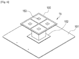
- the antenna unit 15 is disposed in the interior of the box 13.
- the antenna unit 15 includes an antenna 150, an antenna transmission/reception module, a reflective plate 151, a ground plate 152, and a plurality of radiation elements 153.
- the ground plate 152 and the radiation elements 153 are electrically connected to each other to transmit a radiation signal.
- a plurality of radiation elements 153 is provided to have radiation patterns, respectively.
- the radiation patterns may be realized by a tetragonal shape, a circular shape, a tetragonal ring shape, and the like.
- the antenna unit 15 is disposed in the interior of the box 13, the four inner walls 136 of the box act as reflective plates of the antenna.
- the box 13 corresponds to a filter unit of the base station apparatus, and although it is exemplified in the embodiment that the filter has a cavity of a rectangular parallelepiped shape, the present invention is not limited thereto.
- the filter unit has at least two filters coupled to face each other.
- the antenna unit 15 is disposed on the widest of the six outer surfaces. That is, the reflective plate 151 of the antenna unit 15 becomes more helpful in improving RF characteristics as the areas of the reflective plate 151 become wider, and thus it is preferable that the reflective plate 151 is installed on the widest surface as shown in the drawings.
- connection connections may be, for example, cables, and the connection structure may be, for example, a connector or a connection terminal.
- the digital interface module and the antenna unit are stacked in the Z axis direction, but the first and second power amplifiers, the up/down converter, and the power supply unit are disposed along the X and Y axes such that the base station can be made small.
- a plurality of boards are not vertically stacked but are three-dimensionally disposed along the outer surfaces of the box in consideration of heat emission, so that the boards can be efficiently mounted in a limited space.
Landscapes
- Engineering & Computer Science (AREA)
- Computer Networks & Wireless Communication (AREA)
- Signal Processing (AREA)
- Physics & Mathematics (AREA)
- Electromagnetism (AREA)
- Transceivers (AREA)
- Support Of Aerials (AREA)
- Variable-Direction Aerials And Aerial Arrays (AREA)
- Mobile Radio Communication Systems (AREA)
Description
- The present invention relates to a base station of a mobile communication system, and more particularly to a small base station installed in a building or a house.
- A base station of a mobile communication system refers to a system for relaying electric waves of a portable terminal in a cell. The base station is generally installed on a roof of a building to relay electric waves of a portable terminal. Accordingly, base stations are present in units of cells, and the base stations controls transmission of signals, designation of a communication channel, and monitoring of a communication channel in units of cells, as well as an interface function between the portable terminal and a switch center.
- The antennas employed in the base station are distributed due to presence of many control antennas which may be vertically or horizontally beam-tilted.
- In addition, a small base station for improving communication quality while reducing frequency load is installed as a system for covering an area which is still smaller than the radius of the current existing mobile communication service. The base station is used to accommodate data traffic intensively generated in a small area. As a small base station can be installed in a building or a house, a shading area can be solved and a higher network and a convergence service can be realized.
- However, because the small base station employed in the existing mobile communication system is configured such that main components mounted to the interior of the base station, for example, a main board, a power supply unit, an antenna, and a power amplifier are vertically stacked, there is a limit in reducing the entire size of the base station.
- In particular, because the small base station according to the related art is configured such that a main board, a power supply unit and the like are installed on one board, the overall size of the main board become larger and heat emission of the power amplifier becomes problematic.
-
EP 2 389 710 B1 discloses an enclosing and a mounting structure for an antenna comprising a tube that has an outer surface adapted for mounting transmitter and/or receiver components thereon and an inner surface defining a cooling chimney, and a radome which has an opening at each end of the tube for allowing air to circulate through the cooling chimney. The chimney enhances air flow and provides improved heat removal by the airflow. However, a chimney has to be of a certain length in order to provide sufficient air flow, which does not support the desired small size. -
EP 2 408 121 A1 describes a radio frequency unit and an integrated antenna. The radio frequency unit includes a duplexer, a power amplifier circuit board, and a transceiver circuit board. The power amplifier circuit board and the transceiver circuit board are respectively located at two end portions of the duplexer. The power amplifier circuit board and the transceiver circuit board are projected onto the same plane along a direction being vertical to the power amplifier circuit board with their projections on the same plane non-overlapped each other. -
US 2012/014697 A1 describes an antenna device, which includes a first antenna unit and a second antenna unit. The first antenna unit includes a first radiation module, a power divider/combiner network connected to the first radiation module, and a feeder interface connected to the power divider/combiner network. The second antenna unit includes a second radiation module, a transceiver array connected to the second radiation module, a baseband processing unit. - Accordingly, the present invention provides a small base station of a mobile communication system which can advantageously realize a small size by three-dimensionally disposing main elements at proper places with respect to a box.
- The present invention also provides a small base station of a mobile communication system which can minimize a heat emission problem by disposing a plurality of power amplifiers such that they are spaced apart from each other by the farthest distance.
- The above objects are solved by the claimed matter according to the independent claim. The dependent claims contain further improvements to the invention.
- As described above, the digital interface module and the antenna unit are stacked in the Z axis direction, but the first and second power amplifiers, the up/down converter, and the power supply unit are disposed along the X and Y axes such that the base station can be made small. In particular, according to the present invention, a plurality of boards are not vertically stacked but are three-dimensionally disposed along the outer surfaces of the box in consideration of heat emission, so that the boards can be efficiently mounted in a limited space.
-
-
FIG. 1 is a perspective view showing an external appearance of a small base station according to the present invention; -
FIG. 2 is an exploded perspective view showing a configuration of the small base station according to the present invention; -
FIG. 3 is a perspective view showing a box to which an antenna unit of the small base station according to the present invention is mounted, and is a view showing a state in which an antenna is removed from the antenna unit; -
FIG. 4 is a sectional view showing the box to which the antenna unit of the small base station according to the present invention is mounted; -
FIG. 5 is a plan view showing the box to which the antenna unit of the small base station according to the present invention is mounted, and is a view showing a state in which the antenna is removed from the antenna unit; and -
FIG. 6 is a perspective view showing the antenna of the small base station according to the present invention. - The present invention includes: a polyhedral box; an antenna unit installed on the widest one of outer surfaces of the box; a first board disposed on any one of the outer surfaces of the box; and at least two other boards disposed in an upright position from the first board.
- Hereinafter, the present invention will be described with reference to the accompanying drawings. The same reference numerals denote the same elements.
- In the description of the small base station according to the present invention, the Cartesian coordinate system shown in
FIGS. 1 and2 is used, in which the X axis denotes a transverse direction, the Y axis denotes a longitudinal direction, and the Z axis denotes a perpendicular direction. Thebase station 10 according to the present invention is small-sized in a transverse direction, a longitudinal direction, and a perpendicular direction thereof as compared with the related art, but maintains a performance of an existing base station despite the small size. That is, the small size means that the entire size of the base station is small long the three axes as compared with the related art. -
FIG. 1 shows an external appearance of the small base station 10 (hereinafter, simply referred to as a base station) according to the present invention.FIG. 1 shows an assembled state of thebase station 10, and shows an external appearance of thebase station 10 in which anouter cover 11 and aheat sink 12 are coupled to each other. Theheat sink 12 is disposed on the bottom of thebase station 10 to support main elements mounted on theheat sink 12, and theouter cover 11 is coupled to the heat sink in the Z axis direction to protect main internal elements. -
FIG. 2 is an exploded perspective view showing a configuration of thebase station 10 according to the present invention. As shown inFIG. 2 , anantenna unit 15, at least three boards B1 to B4 (printed circuit boards), a power supply unit (PSU) 14, and aheat sink 12, including abox 13, are three-dimensionally disposed at proper locations of thebase station 10. The three-dimensional disposition of the plurality of boards does mean that the boards are not stacked along one axis but the main elements are disposed in consideration of the three axes including the X, Y, and Z axes, and in particular means that a plurality of boards are disposed in a reference board in an upright position along the X and Y axes and the remaining main elements are disposed along the Z axis, which three-dimensional disposition is advantageous in the small-size of the base station. In addition, thebase station 10 according to the present invention considers a heat emission problem as well as the three-dimensional disposition of the main elements. - The
box 13 has a polyhedral shape, for example, a rectangular parallelepiped shape, and includes a plurality of outer surfaces and a plurality of inner walls and theantenna unit 15 is accommodated in the interior space. In particular, thebox 13 has an open-topped box shape, and has at least threeinner walls 136, at least threeouter surfaces 131 to 134, and abottom surface 135. The outer surfaces of the box include at least threeouter surfaces 131 to 134, and abottom surface 135. The inner walls include at least three inner walls.FIGS. 2 and 3 show fourinner walls 136, and fourouter surfaces 131 to 134. The outer surfaces and the inner walls have the same shapes and the same sizes. - The plurality of outer surfaces include first and second
outer surfaces outer surfaces outer surfaces outer surfaces outer surfaces outer surfaces outer surfaces 131 is perpendicular to the third andfourth surfaces outer surface 132 is perpendicular to the third andfourth surfaces outer surfaces 131 to 134 are flat. Because the box has a rectangular parallelepiped shape, the first to fourthouter surfaces 131 to 134 have a rectangular shape. - The
box 13 has a plurality of outer surfaces, in which in the aspect of the shapes of the outer surfaces, the firstouter surface 131 and the secondouter surface 132 may have the same rectangular or square shape, the thirdouter surface 133 and the fourthouter surface 134 may have the same rectangular or square shape, and thebottom surface 135 also may have a rectangular or square shape. - In the aspect of the sizes (areas) of the outer surfaces of the box, the first and second
outer surfaces outer surfaces - The
bottom surface 135 of the outer surfaces, which is located at the bottom of the box, may have a rectangular or square shape, or may have a shape larger than, smaller than, or the same as those of the first and secondouter surfaces outer surfaces box 13 according to the present invention has abottom surface 135 which is wider than the first and secondouter surfaces outer surfaces FIG. 2 shows that the box 2 has abottom surface 135 which is wider than the first and secondouter surfaces outer surfaces bottom surface 135 has the widest area such that theantenna unit 15 is disposed parallel to thebottom surface 135. - In detail, the disposition of the boards mounted to the outer surfaces of the
box 13 will be described. - A plurality of boards B1 to B4, and the
power supply unit 14 are disposed on the outer surfaces of thebox 13. The plurality of boards includes first and fourth boards B1 to B4. The first board B1 is disposed on thebottom surface 135 of thebox 13. The second and third boards B2 and B3 are disposed on the first and secondouter surfaces box 13. The fourth board B4 is disposed on the thirdouter surface 133. Thepower supply unit 14 is disposed on the fourthouter surface 134. - The first board B1 is a digital interface module, and is disposed in parallel to the bottom surface of the
box 135 while facing the bottom surface of thebox 135. The second board B2 is a first power amplifier PAM, and is disposed in parallel to the firstouter surface 131 while facing the firstouter surface 131. The third board B3 is a second power amplifier PAM, and is disposed in parallel to the secondouter surface 132 while facing the secondouter surface 132. The fourth board B4 is an up/down converter, and is disposed in parallel to the thirdouter surface 133 while facing the thirdouter surface 133. Thepower supply unit 14 is disposed in parallel to the fourthouter surface 134 while facing the fourthouter surface 134. - As mentioned above, the first to fourth boards B1 to B4, and the
power supply unit 14 substantially have plate shapes, and may be disposed on the outer surface of the box, in detail, the first to fourthouter surfaces 131 to 134 and thebottom surface 135 are flat so as to have apertures or to be adhered to each other. The first and second power amplifiers B2 and B3 are disposed in parallel to each other while facing each other. The up/down converter B4 and thepower supply unit 14 are disposed in parallel to each other while being spaced apart from each other. - The first and second power amplifiers B2 and B3 are disposed to be spaced apart from each other with respect to the
box 13, in consideration of heat emission efficiency. That is, the first and second power amplifiers B2 and B3 have power amplifying elements (not shown), in consideration of a heat emission problem. That is, when a plurality of power amplifiers B2 and B3 are provided, it is most effective in heat emission to dispose the power amplifiers B2 and B3 such that they are spaced apart from each other at the longest distance possible. It is preferable to dispose the power amplifiers such that they face each other when thebox 13 has a rectangular parallelepiped shape as shown in the drawings, and it is most preferable that the power amplifiers are separated by the largest distance possible when thebox 13 has various shapes. - It will be appreciated by those skilled in the art that the power amplifiers may be disposed in two boards rather than in one board in consideration of the heat emission problem.
- Although it has been exemplified that the first and second power amplifiers B2 and B3 are disposed on the first and second
outer surfaces outer surfaces power supply unit 14 are disposed on the third and fourthouter surfaces outer surfaces outer surfaces power supply unit 14 face each other while being spaced apart from each other. The first power amplifier B2 is perpendicular to the digital interface module B1, the up/down converter B4, and thepower supply unit 14, and the second power amplifier B3 is perpendicular to the digital interface module B1, the up/down converter B4, and thepower supply unit 14. - In the disposition of the plurality of boards of the base station, the second to fourth boards are disposed in upright positions along a peripheral circumference of the first board.
- Referring to
FIGS. 3 to 6 , theantenna unit 15 is disposed in the interior of thebox 13. Theantenna unit 15 includes anantenna 150, an antenna transmission/reception module, areflective plate 151, aground plate 152, and a plurality ofradiation elements 153. Theground plate 152 and theradiation elements 153 are electrically connected to each other to transmit a radiation signal. A plurality ofradiation elements 153 is provided to have radiation patterns, respectively. The radiation patterns may be realized by a tetragonal shape, a circular shape, a tetragonal ring shape, and the like. - As shown in
FIG. 4 , if theantenna unit 15 is disposed in the interior of thebox 13, the fourinner walls 136 of the box act as reflective plates of the antenna. - The
box 13 corresponds to a filter unit of the base station apparatus, and although it is exemplified in the embodiment that the filter has a cavity of a rectangular parallelepiped shape, the present invention is not limited thereto. The filter unit has at least two filters coupled to face each other. - When the
box 13 has a rectangular parallelepiped shape, it is preferable that theantenna unit 15 is disposed on the widest of the six outer surfaces. That is, thereflective plate 151 of theantenna unit 15 becomes more helpful in improving RF characteristics as the areas of thereflective plate 151 become wider, and thus it is preferable that thereflective plate 151 is installed on the widest surface as shown in the drawings. - In the description of the disposition state of the main internal elements of the base station according to the present invention, electrical connections or a connection structure between the main internal elements are omitted. The electrical connections may be, for example, cables, and the connection structure may be, for example, a connector or a connection terminal.
- According to the present invention, the digital interface module and the antenna unit are stacked in the Z axis direction, but the first and second power amplifiers, the up/down converter, and the power supply unit are disposed along the X and Y axes such that the base station can be made small. In particular, according to the present invention, a plurality of boards are not vertically stacked but are three-dimensionally disposed along the outer surfaces of the box in consideration of heat emission, so that the boards can be efficiently mounted in a limited space.
Claims (10)
- A base station (10) of a mobile communication system, comprising:a polyhedral box (13) comprising a plurality of outer surfaces (131-135),an antenna unit (15) installed on the widest of outer surfaces of the box (13),a first board (B1) disposed on one of the outer surfaces (135) of the box (13) opposite to the antenna unit (15); andat least two other boards (B2, B3, B4, 14) disposed on two other outer surfaces (131, 132, 133, 134) of the box (13), wherein the antenna unit (15) is disposed on a surface of the box (13) which is different than the outer surfaces (131-135) of the box (13) on which the first board (B1) and the at least two other boards (B2, B3, B4, 14) are disposed, andwherein the at least two other boards (B2, B3, B4, 14) are first and second power amplifiers,the first and second power amplifiers (B2 and B3) are disposed to be spaced apart from each other on opposite outer surfaces (131, 132 or 133, 134) of the box (13) which face each other.
- The base station of claim 1, wherein the box comprises:first and second outer surfaces (131, 132) which face each other; andthird and fourth outer surfaces (133, 134) disposed between the first and second outer surfaces (131, 132) while facing each other,wherein at least three inner walls (136) are provided inside the outer surface of the box (13) on which the antenna unit (15) is installed.
- The base station of claim 2, wherein second and third boards (B2, B3) are disposed in parallel to the first and second outer surfaces (131, 132) to face the first and second outer surfaces (131, 132), respectively; and
a fourth board (B4) is disposed in parallel to the third outer surface (133) while facing the third outer surface (133). - The base station of claim 3, wherein the first board (B1) is a digital interface module, the second and third boards (B2, B3) are the first and second power amplifiers, and the fourth board (B4) is an up/down converter.
- The base station of claim 3, wherein a power supply unit (14) is disposed on the fourth outer surface (134), and is disposed to be perpendicular to the first board (B1).
- The base station of claim 2, wherein the antenna unit (15) comprises an antenna (150), an antenna transmission/reception module stacked on the antenna (150).
- The base station of claim 6, wherein the inner wall (136) acts as a reflective plate of the antenna unit (15).
- The base station of claim 1, wherein the box (13) is a filter unit.
- The base station of claim 8, wherein the filter unit has at least two filters coupled to face each other.
- The base station of claim 5, wherein the antenna unit (15), the first to fourth boards (B1 - B4) and the power supply unit (14) are disposed to surround all the outer surfaces of the box (13).
Applications Claiming Priority (3)
| Application Number | Priority Date | Filing Date | Title |
|---|---|---|---|
| KR20120086155 | 2012-08-07 | ||
| KR1020120108217A KR101868869B1 (en) | 2012-08-07 | 2012-09-27 | Compact-type base station for mobile communication system |
| PCT/KR2013/007063 WO2014025183A1 (en) | 2012-08-07 | 2013-08-06 | Small base station for mobile communication system |
Publications (3)
| Publication Number | Publication Date |
|---|---|
| EP2884676A1 EP2884676A1 (en) | 2015-06-17 |
| EP2884676A4 EP2884676A4 (en) | 2016-02-24 |
| EP2884676B1 true EP2884676B1 (en) | 2018-09-19 |
Family
ID=50267099
Family Applications (1)
| Application Number | Title | Priority Date | Filing Date |
|---|---|---|---|
| EP13828208.2A Active EP2884676B1 (en) | 2012-08-07 | 2013-08-06 | Small base station for mobile communication system |
Country Status (6)
| Country | Link |
|---|---|
| US (1) | US9491799B2 (en) |
| EP (1) | EP2884676B1 (en) |
| JP (1) | JP5969703B2 (en) |
| KR (1) | KR101868869B1 (en) |
| CN (1) | CN104508995B (en) |
| WO (1) | WO2014025183A1 (en) |
Families Citing this family (8)
| Publication number | Priority date | Publication date | Assignee | Title |
|---|---|---|---|---|
| US9204490B2 (en) * | 2013-12-06 | 2015-12-01 | Huawei Technologies Co., Ltd. | Base station installation apparatus included in base station, and base station |
| US10044098B2 (en) * | 2016-02-19 | 2018-08-07 | Facebook, Inc. | Modular base station |
| JP2019527522A (en) | 2016-07-27 | 2019-09-26 | 華為技術有限公司Huawei Technologies Co.,Ltd. | Radio transceiver apparatus and base station |
| KR101855139B1 (en) * | 2016-11-16 | 2018-05-08 | 주식회사 케이엠더블유 | Calibration in MIMO antenna |
| US10629997B2 (en) * | 2016-12-27 | 2020-04-21 | Tongyu Communication Inc. | Radiating integrated antenna unit and multi-array antenna of same |
| CN110521056B (en) * | 2017-03-31 | 2021-08-03 | 株式会社Kmw | Antenna assembly and device comprising same |
| WO2019136483A1 (en) * | 2018-01-08 | 2019-07-11 | Ubicquia Llc | Camouflaged small cell networking devices |
| KR102290036B1 (en) * | 2019-05-15 | 2021-08-18 | 주식회사 케이엠더블유 | Antenna apparatus |
Family Cites Families (21)
| Publication number | Priority date | Publication date | Assignee | Title |
|---|---|---|---|---|
| JPS6424636A (en) * | 1987-07-21 | 1989-01-26 | Sharp Kk | Microwave converter |
| JP2782213B2 (en) * | 1988-12-16 | 1998-07-30 | オムロン株式会社 | Switching power supply |
| JPH04113724A (en) | 1990-09-03 | 1992-04-15 | Matsushita Electric Ind Co Ltd | Microconverter for satellite communication |
| JP2560293Y2 (en) | 1991-03-26 | 1998-01-21 | 日産ディーゼル工業株式会社 | Exhaust gas purification device for internal combustion engine |
| GB2298995A (en) * | 1995-03-07 | 1996-09-18 | Motorola Ltd | Base station |
| JP4113724B2 (en) | 2002-05-07 | 2008-07-09 | 美和ロック株式会社 | Variable lever tumbler lock |
| JP2004235840A (en) * | 2003-01-29 | 2004-08-19 | Hitachi Kokusai Electric Inc | Wireless device and antenna sharing device |
| JP3783006B2 (en) * | 2003-07-01 | 2006-06-07 | 株式会社バッファロー | Antenna device |
| KR100611806B1 (en) * | 2004-03-03 | 2006-08-10 | 주식회사 케이엠더블유 | Dual polarization base station antenna be arrayed patch antenna of probe feed and control system of the same |
| JP2007531388A (en) * | 2004-03-26 | 2007-11-01 | アンドリュー・コーポレーション | Base station for mobile communication system |
| SE0401800D0 (en) * | 2004-07-08 | 2004-07-08 | Andrew Corp | Shielding device in a base station |
| JP2008244185A (en) * | 2007-03-28 | 2008-10-09 | Kyocera Corp | Base station for communication |
| JP2009027539A (en) * | 2007-07-20 | 2009-02-05 | Sony Corp | Wireless receiver, and antenna selection method for spatially multiplexed communication |
| JP2009230505A (en) * | 2008-03-24 | 2009-10-08 | Fujitsu Ltd | Board unit and electronic apparatus |
| EP2113963A1 (en) * | 2008-05-02 | 2009-11-04 | Nokia Siemens Networks Oy | An enclosure and mounting assembly for an antenna |
| US8497813B2 (en) * | 2008-12-02 | 2013-07-30 | Andrew Llc | Panel antenna having sealed radio enclosure |
| EP2408121B1 (en) * | 2009-03-13 | 2015-10-28 | Huawei Technologies Co., Ltd. | Radio frequency unit and integrated antenna |
| CN102308437B (en) * | 2009-05-26 | 2013-09-11 | 华为技术有限公司 | Antenna device |
| CN101995926A (en) * | 2009-08-25 | 2011-03-30 | 鸿富锦精密工业(深圳)有限公司 | Computer case and hard disk bracket thereon |
| KR20110035577A (en) * | 2009-09-30 | 2011-04-06 | 주식회사 아모텍 | Internal antenna apparatus for low frequency band |
| US20120286598A1 (en) | 2009-12-18 | 2012-11-15 | Sensoplan Gmbh | Rotor of an Electric Generator for Generating Electricity in Power Plants |
-
2012
- 2012-09-27 KR KR1020120108217A patent/KR101868869B1/en active IP Right Grant
-
2013
- 2013-08-06 EP EP13828208.2A patent/EP2884676B1/en active Active
- 2013-08-06 CN CN201380041941.3A patent/CN104508995B/en active Active
- 2013-08-06 JP JP2015523025A patent/JP5969703B2/en active Active
- 2013-08-06 WO PCT/KR2013/007063 patent/WO2014025183A1/en active Application Filing
-
2015
- 2015-02-05 US US14/615,087 patent/US9491799B2/en active Active
Non-Patent Citations (1)
| Title |
|---|
| None * |
Also Published As
| Publication number | Publication date |
|---|---|
| EP2884676A4 (en) | 2016-02-24 |
| EP2884676A1 (en) | 2015-06-17 |
| JP5969703B2 (en) | 2016-08-17 |
| US20150156818A1 (en) | 2015-06-04 |
| JP2015531190A (en) | 2015-10-29 |
| WO2014025183A1 (en) | 2014-02-13 |
| US9491799B2 (en) | 2016-11-08 |
| CN104508995B (en) | 2018-12-04 |
| KR101868869B1 (en) | 2018-06-19 |
| CN104508995A (en) | 2015-04-08 |
| KR20140019717A (en) | 2014-02-17 |
Similar Documents
| Publication | Publication Date | Title |
|---|---|---|
| EP2884676B1 (en) | Small base station for mobile communication system | |
| KR101769524B1 (en) | Small-sized base station device in mobile communication system | |
| US10790578B2 (en) | Modular small cell architecture | |
| US10283849B2 (en) | Antenna device | |
| JP6918136B2 (en) | Modular radios and radio assemblies with interconnects | |
| CN110034370B (en) | Wireless communication device and method for installing wireless communication device | |
| US9888391B2 (en) | Ultra-wideband active antenna platform | |
| EP2983302B1 (en) | Radio frequency unit and integrated antenna with improved heat dissipation | |
| CN102696150B (en) | Panel antenna having sealed radio enclosure | |
| EP2698922B1 (en) | Radio Remote Unit Device and Assembly Thereof | |
| CN104145372A (en) | Apparatus and method for modular multi-sector active antenna system | |
| CN102369635B (en) | Panel antenna having sealed radio enclosure | |
| EP3570444A1 (en) | Fiber integrated radio equipment for network optimization and densification ecosystem (fire-node) | |
| US20160359237A1 (en) | Wideband antenna star array | |
| KR100724812B1 (en) | Architecture of a base station of a radio communications system | |
| CN217088172U (en) | Integrated base station satellite antenna | |
| WO2024104027A1 (en) | Antenna and base station | |
| CN216354781U (en) | Communication antenna and communication antenna device | |
| CN112821068B (en) | Antenna module and customer premises equipment | |
| CN114765300A (en) | Antenna device and electronic apparatus |
Legal Events
| Date | Code | Title | Description |
|---|---|---|---|
| PUAI | Public reference made under article 153(3) epc to a published international application that has entered the european phase |
Free format text: ORIGINAL CODE: 0009012 |
|
| 17P | Request for examination filed |
Effective date: 20150127 |
|
| AK | Designated contracting states |
Kind code of ref document: A1 Designated state(s): AL AT BE BG CH CY CZ DE DK EE ES FI FR GB GR HR HU IE IS IT LI LT LU LV MC MK MT NL NO PL PT RO RS SE SI SK SM TR |
|
| AX | Request for extension of the european patent |
Extension state: BA ME |
|
| DAX | Request for extension of the european patent (deleted) | ||
| RA4 | Supplementary search report drawn up and despatched (corrected) |
Effective date: 20160127 |
|
| RIC1 | Information provided on ipc code assigned before grant |
Ipc: H01Q 1/24 20060101ALI20160121BHEP Ipc: H01Q 1/02 20060101ALI20160121BHEP Ipc: H04B 7/155 20060101AFI20160121BHEP Ipc: H04Q 1/02 20060101ALI20160121BHEP Ipc: H04W 88/08 20090101ALI20160121BHEP Ipc: H01Q 21/26 20060101ALI20160121BHEP |
|
| STAA | Information on the status of an ep patent application or granted ep patent |
Free format text: STATUS: EXAMINATION IS IN PROGRESS |
|
| 17Q | First examination report despatched |
Effective date: 20170530 |
|
| GRAP | Despatch of communication of intention to grant a patent |
Free format text: ORIGINAL CODE: EPIDOSNIGR1 |
|
| STAA | Information on the status of an ep patent application or granted ep patent |
Free format text: STATUS: GRANT OF PATENT IS INTENDED |
|
| INTG | Intention to grant announced |
Effective date: 20180316 |
|
| GRAS | Grant fee paid |
Free format text: ORIGINAL CODE: EPIDOSNIGR3 |
|
| GRAA | (expected) grant |
Free format text: ORIGINAL CODE: 0009210 |
|
| STAA | Information on the status of an ep patent application or granted ep patent |
Free format text: STATUS: THE PATENT HAS BEEN GRANTED |
|
| AK | Designated contracting states |
Kind code of ref document: B1 Designated state(s): AL AT BE BG CH CY CZ DE DK EE ES FI FR GB GR HR HU IE IS IT LI LT LU LV MC MK MT NL NO PL PT RO RS SE SI SK SM TR |
|
| REG | Reference to a national code |
Ref country code: GB Ref legal event code: FG4D |
|
| REG | Reference to a national code |
Ref country code: CH Ref legal event code: EP |
|
| REG | Reference to a national code |
Ref country code: AT Ref legal event code: REF Ref document number: 1044477 Country of ref document: AT Kind code of ref document: T Effective date: 20181015 |
|
| REG | Reference to a national code |
Ref country code: IE Ref legal event code: FG4D |
|
| REG | Reference to a national code |
Ref country code: DE Ref legal event code: R096 Ref document number: 602013043996 Country of ref document: DE |
|
| REG | Reference to a national code |
Ref country code: SE Ref legal event code: TRGR |
|
| REG | Reference to a national code |
Ref country code: NL Ref legal event code: MP Effective date: 20180919 |
|
| PG25 | Lapsed in a contracting state [announced via postgrant information from national office to epo] |
Ref country code: LT Free format text: LAPSE BECAUSE OF FAILURE TO SUBMIT A TRANSLATION OF THE DESCRIPTION OR TO PAY THE FEE WITHIN THE PRESCRIBED TIME-LIMIT Effective date: 20180919 Ref country code: GR Free format text: LAPSE BECAUSE OF FAILURE TO SUBMIT A TRANSLATION OF THE DESCRIPTION OR TO PAY THE FEE WITHIN THE PRESCRIBED TIME-LIMIT Effective date: 20181220 Ref country code: RS Free format text: LAPSE BECAUSE OF FAILURE TO SUBMIT A TRANSLATION OF THE DESCRIPTION OR TO PAY THE FEE WITHIN THE PRESCRIBED TIME-LIMIT Effective date: 20180919 Ref country code: BG Free format text: LAPSE BECAUSE OF FAILURE TO SUBMIT A TRANSLATION OF THE DESCRIPTION OR TO PAY THE FEE WITHIN THE PRESCRIBED TIME-LIMIT Effective date: 20181219 Ref country code: NO Free format text: LAPSE BECAUSE OF FAILURE TO SUBMIT A TRANSLATION OF THE DESCRIPTION OR TO PAY THE FEE WITHIN THE PRESCRIBED TIME-LIMIT Effective date: 20181219 |
|
| REG | Reference to a national code |
Ref country code: LT Ref legal event code: MG4D |
|
| PG25 | Lapsed in a contracting state [announced via postgrant information from national office to epo] |
Ref country code: AL Free format text: LAPSE BECAUSE OF FAILURE TO SUBMIT A TRANSLATION OF THE DESCRIPTION OR TO PAY THE FEE WITHIN THE PRESCRIBED TIME-LIMIT Effective date: 20180919 Ref country code: LV Free format text: LAPSE BECAUSE OF FAILURE TO SUBMIT A TRANSLATION OF THE DESCRIPTION OR TO PAY THE FEE WITHIN THE PRESCRIBED TIME-LIMIT Effective date: 20180919 Ref country code: HR Free format text: LAPSE BECAUSE OF FAILURE TO SUBMIT A TRANSLATION OF THE DESCRIPTION OR TO PAY THE FEE WITHIN THE PRESCRIBED TIME-LIMIT Effective date: 20180919 |
|
| REG | Reference to a national code |
Ref country code: AT Ref legal event code: MK05 Ref document number: 1044477 Country of ref document: AT Kind code of ref document: T Effective date: 20180919 |
|
| PG25 | Lapsed in a contracting state [announced via postgrant information from national office to epo] |
Ref country code: IT Free format text: LAPSE BECAUSE OF FAILURE TO SUBMIT A TRANSLATION OF THE DESCRIPTION OR TO PAY THE FEE WITHIN THE PRESCRIBED TIME-LIMIT Effective date: 20180919 Ref country code: AT Free format text: LAPSE BECAUSE OF FAILURE TO SUBMIT A TRANSLATION OF THE DESCRIPTION OR TO PAY THE FEE WITHIN THE PRESCRIBED TIME-LIMIT Effective date: 20180919 Ref country code: EE Free format text: LAPSE BECAUSE OF FAILURE TO SUBMIT A TRANSLATION OF THE DESCRIPTION OR TO PAY THE FEE WITHIN THE PRESCRIBED TIME-LIMIT Effective date: 20180919 Ref country code: IS Free format text: LAPSE BECAUSE OF FAILURE TO SUBMIT A TRANSLATION OF THE DESCRIPTION OR TO PAY THE FEE WITHIN THE PRESCRIBED TIME-LIMIT Effective date: 20190119 Ref country code: PL Free format text: LAPSE BECAUSE OF FAILURE TO SUBMIT A TRANSLATION OF THE DESCRIPTION OR TO PAY THE FEE WITHIN THE PRESCRIBED TIME-LIMIT Effective date: 20180919 Ref country code: ES Free format text: LAPSE BECAUSE OF FAILURE TO SUBMIT A TRANSLATION OF THE DESCRIPTION OR TO PAY THE FEE WITHIN THE PRESCRIBED TIME-LIMIT Effective date: 20180919 Ref country code: RO Free format text: LAPSE BECAUSE OF FAILURE TO SUBMIT A TRANSLATION OF THE DESCRIPTION OR TO PAY THE FEE WITHIN THE PRESCRIBED TIME-LIMIT Effective date: 20180919 Ref country code: CZ Free format text: LAPSE BECAUSE OF FAILURE TO SUBMIT A TRANSLATION OF THE DESCRIPTION OR TO PAY THE FEE WITHIN THE PRESCRIBED TIME-LIMIT Effective date: 20180919 Ref country code: NL Free format text: LAPSE BECAUSE OF FAILURE TO SUBMIT A TRANSLATION OF THE DESCRIPTION OR TO PAY THE FEE WITHIN THE PRESCRIBED TIME-LIMIT Effective date: 20180919 |
|
| PG25 | Lapsed in a contracting state [announced via postgrant information from national office to epo] |
Ref country code: SM Free format text: LAPSE BECAUSE OF FAILURE TO SUBMIT A TRANSLATION OF THE DESCRIPTION OR TO PAY THE FEE WITHIN THE PRESCRIBED TIME-LIMIT Effective date: 20180919 Ref country code: PT Free format text: LAPSE BECAUSE OF FAILURE TO SUBMIT A TRANSLATION OF THE DESCRIPTION OR TO PAY THE FEE WITHIN THE PRESCRIBED TIME-LIMIT Effective date: 20190119 Ref country code: SK Free format text: LAPSE BECAUSE OF FAILURE TO SUBMIT A TRANSLATION OF THE DESCRIPTION OR TO PAY THE FEE WITHIN THE PRESCRIBED TIME-LIMIT Effective date: 20180919 |
|
| REG | Reference to a national code |
Ref country code: DE Ref legal event code: R097 Ref document number: 602013043996 Country of ref document: DE |
|
| PLBE | No opposition filed within time limit |
Free format text: ORIGINAL CODE: 0009261 |
|
| STAA | Information on the status of an ep patent application or granted ep patent |
Free format text: STATUS: NO OPPOSITION FILED WITHIN TIME LIMIT |
|
| PG25 | Lapsed in a contracting state [announced via postgrant information from national office to epo] |
Ref country code: DK Free format text: LAPSE BECAUSE OF FAILURE TO SUBMIT A TRANSLATION OF THE DESCRIPTION OR TO PAY THE FEE WITHIN THE PRESCRIBED TIME-LIMIT Effective date: 20180919 |
|
| 26N | No opposition filed |
Effective date: 20190620 |
|
| PG25 | Lapsed in a contracting state [announced via postgrant information from national office to epo] |
Ref country code: SI Free format text: LAPSE BECAUSE OF FAILURE TO SUBMIT A TRANSLATION OF THE DESCRIPTION OR TO PAY THE FEE WITHIN THE PRESCRIBED TIME-LIMIT Effective date: 20180919 |
|
| PG25 | Lapsed in a contracting state [announced via postgrant information from national office to epo] |
Ref country code: TR Free format text: LAPSE BECAUSE OF FAILURE TO SUBMIT A TRANSLATION OF THE DESCRIPTION OR TO PAY THE FEE WITHIN THE PRESCRIBED TIME-LIMIT Effective date: 20180919 |
|
| GBPC | Gb: european patent ceased through non-payment of renewal fee |
Effective date: 20190806 |
|
| PG25 | Lapsed in a contracting state [announced via postgrant information from national office to epo] |
Ref country code: CH Free format text: LAPSE BECAUSE OF NON-PAYMENT OF DUE FEES Effective date: 20190831 Ref country code: LU Free format text: LAPSE BECAUSE OF NON-PAYMENT OF DUE FEES Effective date: 20190806 Ref country code: MC Free format text: LAPSE BECAUSE OF FAILURE TO SUBMIT A TRANSLATION OF THE DESCRIPTION OR TO PAY THE FEE WITHIN THE PRESCRIBED TIME-LIMIT Effective date: 20180919 Ref country code: LI Free format text: LAPSE BECAUSE OF NON-PAYMENT OF DUE FEES Effective date: 20190831 |
|
| REG | Reference to a national code |
Ref country code: BE Ref legal event code: MM Effective date: 20190831 |
|
| PG25 | Lapsed in a contracting state [announced via postgrant information from national office to epo] |
Ref country code: FR Free format text: LAPSE BECAUSE OF NON-PAYMENT OF DUE FEES Effective date: 20190831 Ref country code: IE Free format text: LAPSE BECAUSE OF NON-PAYMENT OF DUE FEES Effective date: 20190806 |
|
| PG25 | Lapsed in a contracting state [announced via postgrant information from national office to epo] |
Ref country code: GB Free format text: LAPSE BECAUSE OF NON-PAYMENT OF DUE FEES Effective date: 20190806 Ref country code: BE Free format text: LAPSE BECAUSE OF NON-PAYMENT OF DUE FEES Effective date: 20190831 |
|
| REG | Reference to a national code |
Ref country code: DE Ref legal event code: R082 Ref document number: 602013043996 Country of ref document: DE Representative=s name: SCHEELE JAEGER WETZEL PATENTANWAELTE PARTNERSC, DE Ref country code: DE Ref legal event code: R082 Ref document number: 602013043996 Country of ref document: DE Representative=s name: SCHEELE WETZEL PATENTANWAELTE, DE Ref country code: DE Ref legal event code: R082 Ref document number: 602013043996 Country of ref document: DE Representative=s name: SCHEELE WETZEL PATENTANWAELTE PARTNERSCHAFTSGE, DE |
|
| PG25 | Lapsed in a contracting state [announced via postgrant information from national office to epo] |
Ref country code: CY Free format text: LAPSE BECAUSE OF FAILURE TO SUBMIT A TRANSLATION OF THE DESCRIPTION OR TO PAY THE FEE WITHIN THE PRESCRIBED TIME-LIMIT Effective date: 20180919 |
|
| PG25 | Lapsed in a contracting state [announced via postgrant information from national office to epo] |
Ref country code: MT Free format text: LAPSE BECAUSE OF FAILURE TO SUBMIT A TRANSLATION OF THE DESCRIPTION OR TO PAY THE FEE WITHIN THE PRESCRIBED TIME-LIMIT Effective date: 20180919 Ref country code: HU Free format text: LAPSE BECAUSE OF FAILURE TO SUBMIT A TRANSLATION OF THE DESCRIPTION OR TO PAY THE FEE WITHIN THE PRESCRIBED TIME-LIMIT; INVALID AB INITIO Effective date: 20130806 |
|
| PG25 | Lapsed in a contracting state [announced via postgrant information from national office to epo] |
Ref country code: MK Free format text: LAPSE BECAUSE OF FAILURE TO SUBMIT A TRANSLATION OF THE DESCRIPTION OR TO PAY THE FEE WITHIN THE PRESCRIBED TIME-LIMIT Effective date: 20180919 |
|
| PGFP | Annual fee paid to national office [announced via postgrant information from national office to epo] |
Ref country code: SE Payment date: 20230613 Year of fee payment: 11 |
|
| PGFP | Annual fee paid to national office [announced via postgrant information from national office to epo] |
Ref country code: FI Payment date: 20230816 Year of fee payment: 11 |
|
| PGFP | Annual fee paid to national office [announced via postgrant information from national office to epo] |
Ref country code: DE Payment date: 20230613 Year of fee payment: 11 |