EP2884242B1 - Sensor Package And Manufacturing Method - Google Patents
Sensor Package And Manufacturing Method Download PDFInfo
- Publication number
- EP2884242B1 EP2884242B1 EP13196851.3A EP13196851A EP2884242B1 EP 2884242 B1 EP2884242 B1 EP 2884242B1 EP 13196851 A EP13196851 A EP 13196851A EP 2884242 B1 EP2884242 B1 EP 2884242B1
- Authority
- EP
- European Patent Office
- Prior art keywords
- intermediate carrier
- chip
- sensor
- package
- outer edge
- Prior art date
- Legal status (The legal status is an assumption and is not a legal conclusion. Google has not performed a legal analysis and makes no representation as to the accuracy of the status listed.)
- Not-in-force
Links
Images

Classifications
-
- H—ELECTRICITY
- H10—SEMICONDUCTOR DEVICES; ELECTRIC SOLID-STATE DEVICES NOT OTHERWISE PROVIDED FOR
- H10W—GENERIC PACKAGES, INTERCONNECTIONS, CONNECTORS OR OTHER CONSTRUCTIONAL DETAILS OF DEVICES COVERED BY CLASS H10
- H10W72/00—Interconnections or connectors in packages
- H10W72/20—Bump connectors, e.g. solder bumps or copper pillars; Dummy bumps; Thermal bumps
-
- G—PHYSICS
- G01—MEASURING; TESTING
- G01D—MEASURING NOT SPECIALLY ADAPTED FOR A SPECIFIC VARIABLE; ARRANGEMENTS FOR MEASURING TWO OR MORE VARIABLES NOT COVERED IN A SINGLE OTHER SUBCLASS; TARIFF METERING APPARATUS; MEASURING OR TESTING NOT OTHERWISE PROVIDED FOR
- G01D11/00—Component parts of measuring arrangements not specially adapted for a specific variable
- G01D11/24—Housings ; Casings for instruments
- G01D11/245—Housings for sensors
-
- H—ELECTRICITY
- H10—SEMICONDUCTOR DEVICES; ELECTRIC SOLID-STATE DEVICES NOT OTHERWISE PROVIDED FOR
- H10W—GENERIC PACKAGES, INTERCONNECTIONS, CONNECTORS OR OTHER CONSTRUCTIONAL DETAILS OF DEVICES COVERED BY CLASS H10
- H10W72/00—Interconnections or connectors in packages
- H10W72/30—Die-attach connectors
-
- H—ELECTRICITY
- H10—SEMICONDUCTOR DEVICES; ELECTRIC SOLID-STATE DEVICES NOT OTHERWISE PROVIDED FOR
- H10W—GENERIC PACKAGES, INTERCONNECTIONS, CONNECTORS OR OTHER CONSTRUCTIONAL DETAILS OF DEVICES COVERED BY CLASS H10
- H10W74/00—Encapsulations, e.g. protective coatings
- H10W74/01—Manufacture or treatment
- H10W74/016—Manufacture or treatment using moulds
-
- H—ELECTRICITY
- H10—SEMICONDUCTOR DEVICES; ELECTRIC SOLID-STATE DEVICES NOT OTHERWISE PROVIDED FOR
- H10W—GENERIC PACKAGES, INTERCONNECTIONS, CONNECTORS OR OTHER CONSTRUCTIONAL DETAILS OF DEVICES COVERED BY CLASS H10
- H10W74/00—Encapsulations, e.g. protective coatings
- H10W74/10—Encapsulations, e.g. protective coatings characterised by their shape or disposition
- H10W74/111—Encapsulations, e.g. protective coatings characterised by their shape or disposition the semiconductor body being completely enclosed
-
- H—ELECTRICITY
- H10—SEMICONDUCTOR DEVICES; ELECTRIC SOLID-STATE DEVICES NOT OTHERWISE PROVIDED FOR
- H10W—GENERIC PACKAGES, INTERCONNECTIONS, CONNECTORS OR OTHER CONSTRUCTIONAL DETAILS OF DEVICES COVERED BY CLASS H10
- H10W74/00—Encapsulations, e.g. protective coatings
- H10W74/10—Encapsulations, e.g. protective coatings characterised by their shape or disposition
- H10W74/111—Encapsulations, e.g. protective coatings characterised by their shape or disposition the semiconductor body being completely enclosed
- H10W74/114—Encapsulations, e.g. protective coatings characterised by their shape or disposition the semiconductor body being completely enclosed by a substrate and the encapsulations
-
- H—ELECTRICITY
- H10—SEMICONDUCTOR DEVICES; ELECTRIC SOLID-STATE DEVICES NOT OTHERWISE PROVIDED FOR
- H10W—GENERIC PACKAGES, INTERCONNECTIONS, CONNECTORS OR OTHER CONSTRUCTIONAL DETAILS OF DEVICES COVERED BY CLASS H10
- H10W72/00—Interconnections or connectors in packages
- H10W72/071—Connecting or disconnecting
- H10W72/072—Connecting or disconnecting of bump connectors
- H10W72/07231—Techniques
- H10W72/07236—Soldering or alloying
-
- H—ELECTRICITY
- H10—SEMICONDUCTOR DEVICES; ELECTRIC SOLID-STATE DEVICES NOT OTHERWISE PROVIDED FOR
- H10W—GENERIC PACKAGES, INTERCONNECTIONS, CONNECTORS OR OTHER CONSTRUCTIONAL DETAILS OF DEVICES COVERED BY CLASS H10
- H10W72/00—Interconnections or connectors in packages
- H10W72/071—Connecting or disconnecting
- H10W72/072—Connecting or disconnecting of bump connectors
- H10W72/07251—Connecting or disconnecting of bump connectors characterised by changes in properties of the bump connectors during connecting
- H10W72/07254—Connecting or disconnecting of bump connectors characterised by changes in properties of the bump connectors during connecting changes in dispositions
-
- H—ELECTRICITY
- H10—SEMICONDUCTOR DEVICES; ELECTRIC SOLID-STATE DEVICES NOT OTHERWISE PROVIDED FOR
- H10W—GENERIC PACKAGES, INTERCONNECTIONS, CONNECTORS OR OTHER CONSTRUCTIONAL DETAILS OF DEVICES COVERED BY CLASS H10
- H10W72/00—Interconnections or connectors in packages
- H10W72/071—Connecting or disconnecting
- H10W72/073—Connecting or disconnecting of die-attach connectors
- H10W72/07331—Connecting techniques
- H10W72/07337—Connecting techniques using a polymer adhesive, e.g. an adhesive based on silicone or epoxy
-
- H—ELECTRICITY
- H10—SEMICONDUCTOR DEVICES; ELECTRIC SOLID-STATE DEVICES NOT OTHERWISE PROVIDED FOR
- H10W—GENERIC PACKAGES, INTERCONNECTIONS, CONNECTORS OR OTHER CONSTRUCTIONAL DETAILS OF DEVICES COVERED BY CLASS H10
- H10W72/00—Interconnections or connectors in packages
- H10W72/071—Connecting or disconnecting
- H10W72/074—Connecting or disconnecting of anisotropic conductive adhesives
-
- H—ELECTRICITY
- H10—SEMICONDUCTOR DEVICES; ELECTRIC SOLID-STATE DEVICES NOT OTHERWISE PROVIDED FOR
- H10W—GENERIC PACKAGES, INTERCONNECTIONS, CONNECTORS OR OTHER CONSTRUCTIONAL DETAILS OF DEVICES COVERED BY CLASS H10
- H10W72/00—Interconnections or connectors in packages
- H10W72/20—Bump connectors, e.g. solder bumps or copper pillars; Dummy bumps; Thermal bumps
- H10W72/241—Dispositions, e.g. layouts
- H10W72/242—Dispositions, e.g. layouts relative to the surface, e.g. recessed, protruding
-
- H—ELECTRICITY
- H10—SEMICONDUCTOR DEVICES; ELECTRIC SOLID-STATE DEVICES NOT OTHERWISE PROVIDED FOR
- H10W—GENERIC PACKAGES, INTERCONNECTIONS, CONNECTORS OR OTHER CONSTRUCTIONAL DETAILS OF DEVICES COVERED BY CLASS H10
- H10W72/00—Interconnections or connectors in packages
- H10W72/20—Bump connectors, e.g. solder bumps or copper pillars; Dummy bumps; Thermal bumps
- H10W72/251—Materials
- H10W72/252—Materials comprising solid metals or solid metalloids, e.g. PbSn, Ag or Cu
-
- H—ELECTRICITY
- H10—SEMICONDUCTOR DEVICES; ELECTRIC SOLID-STATE DEVICES NOT OTHERWISE PROVIDED FOR
- H10W—GENERIC PACKAGES, INTERCONNECTIONS, CONNECTORS OR OTHER CONSTRUCTIONAL DETAILS OF DEVICES COVERED BY CLASS H10
- H10W72/00—Interconnections or connectors in packages
- H10W72/50—Bond wires
- H10W72/531—Shapes of wire connectors
- H10W72/536—Shapes of wire connectors the connected ends being ball-shaped
-
- H—ELECTRICITY
- H10—SEMICONDUCTOR DEVICES; ELECTRIC SOLID-STATE DEVICES NOT OTHERWISE PROVIDED FOR
- H10W—GENERIC PACKAGES, INTERCONNECTIONS, CONNECTORS OR OTHER CONSTRUCTIONAL DETAILS OF DEVICES COVERED BY CLASS H10
- H10W72/00—Interconnections or connectors in packages
- H10W72/50—Bond wires
- H10W72/531—Shapes of wire connectors
- H10W72/5363—Shapes of wire connectors the connected ends being wedge-shaped
-
- H—ELECTRICITY
- H10—SEMICONDUCTOR DEVICES; ELECTRIC SOLID-STATE DEVICES NOT OTHERWISE PROVIDED FOR
- H10W—GENERIC PACKAGES, INTERCONNECTIONS, CONNECTORS OR OTHER CONSTRUCTIONAL DETAILS OF DEVICES COVERED BY CLASS H10
- H10W74/00—Encapsulations, e.g. protective coatings
-
- H—ELECTRICITY
- H10—SEMICONDUCTOR DEVICES; ELECTRIC SOLID-STATE DEVICES NOT OTHERWISE PROVIDED FOR
- H10W—GENERIC PACKAGES, INTERCONNECTIONS, CONNECTORS OR OTHER CONSTRUCTIONAL DETAILS OF DEVICES COVERED BY CLASS H10
- H10W74/00—Encapsulations, e.g. protective coatings
- H10W74/10—Encapsulations, e.g. protective coatings characterised by their shape or disposition
-
- H—ELECTRICITY
- H10—SEMICONDUCTOR DEVICES; ELECTRIC SOLID-STATE DEVICES NOT OTHERWISE PROVIDED FOR
- H10W—GENERIC PACKAGES, INTERCONNECTIONS, CONNECTORS OR OTHER CONSTRUCTIONAL DETAILS OF DEVICES COVERED BY CLASS H10
- H10W90/00—Package configurations
- H10W90/701—Package configurations characterised by the relative positions of pads or connectors relative to package parts
- H10W90/721—Package configurations characterised by the relative positions of pads or connectors relative to package parts of bump connectors
- H10W90/724—Package configurations characterised by the relative positions of pads or connectors relative to package parts of bump connectors between a chip and a stacked insulating package substrate, interposer or RDL
-
- H—ELECTRICITY
- H10—SEMICONDUCTOR DEVICES; ELECTRIC SOLID-STATE DEVICES NOT OTHERWISE PROVIDED FOR
- H10W—GENERIC PACKAGES, INTERCONNECTIONS, CONNECTORS OR OTHER CONSTRUCTIONAL DETAILS OF DEVICES COVERED BY CLASS H10
- H10W90/00—Package configurations
- H10W90/701—Package configurations characterised by the relative positions of pads or connectors relative to package parts
- H10W90/721—Package configurations characterised by the relative positions of pads or connectors relative to package parts of bump connectors
- H10W90/726—Package configurations characterised by the relative positions of pads or connectors relative to package parts of bump connectors between a chip and a stacked lead frame, conducting package substrate or heat sink
-
- H—ELECTRICITY
- H10—SEMICONDUCTOR DEVICES; ELECTRIC SOLID-STATE DEVICES NOT OTHERWISE PROVIDED FOR
- H10W—GENERIC PACKAGES, INTERCONNECTIONS, CONNECTORS OR OTHER CONSTRUCTIONAL DETAILS OF DEVICES COVERED BY CLASS H10
- H10W90/00—Package configurations
- H10W90/701—Package configurations characterised by the relative positions of pads or connectors relative to package parts
- H10W90/751—Package configurations characterised by the relative positions of pads or connectors relative to package parts of bond wires
- H10W90/756—Package configurations characterised by the relative positions of pads or connectors relative to package parts of bond wires between a chip and a stacked lead frame, conducting package substrate or heat sink
Definitions
- This application relates to sensor chip packages.
- Quad flat packages are one example of surface mount integrated circuit package, in which gull wing leads extend from each of the four sides of the package.
- HVQFN Heatsink Very-thin Quad Flat-pack No-leads package
- This is a package with no component leads extending from the package, and in which the package includes an integrated heat sink part.
- the package is for mounting on a printed circuit board by soldering, with other surface mount devices.
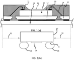
- Figure 1(a) shows a HVQFN package for soldering onto a PCB.
- the sensor chip 10 has pads 11 around the outer region of the top surface. In one example these pads connect to bond wires 14 which extend down to a carrier 12 such as a lead frame, which provides a fan out function.
- the bond wires are embedded in the package.
- the bond wires are connected by means of wirebonding. This is usually a "cold welding" process in the sense that the materials that are joined are not brought into the liquid state (as in real welding and soldering processes).
- a metallization is present on the bond pads when an IC is intended for wirebonding, and this is often aluminum or gold.
- the lead frame 12 has outer contacts which are soldered to an underlying PCB 13, and a central die pad area beneath the chip 10.
- the central die pad area is also soldered to the PCB, and this solder region performs a heat sink function.
- the carrier can for example be a laminate substrate.
- the chip 10 carries one or more sensor elements 16.
- a HVQFN cavity package allows for the sensors on the chip to have an open access to the environment by providing package encapsulation with an opening through which the sensor area is exposed.
- Figure 1(b) shows a sensor chip with solder bumps 18 on the pads 11 which could be used to enable the chip to be mounted directly onto a PCB.
- a disadvantage of the package of Figure 1(a) is that the package size is relatively large compared to the die size, as represented by arrows 20.
- CSP chip scale package
- the disadvantage of this approach for sensors is the risk of contamination from the CSP process, in particular the risk of solder splatter when solder bumps are reflow soldered when those solder bumps are attached at the wafer level, but also during the board soldering process at the customer side which might pollute the sensor area, and affect its functionality.
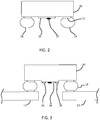
- Figures 2 and 3 are used to illustrate the problems of soldering the chip directly to a PCB.
- Figure 2 shows how the sensor element 16 can be polluted by the CSP process when being prepared for soldering to a PCB, in particular when forming the solder balls 18.
- the process starts with a wafer, on which the bond pads 11 are formed, followed by an under bump metallisation.
- the solder balls are applied by a reflow process, which can give rise to the pollutant shown as 22.
- the resulting package is then soldered at the customer side (i.e. a producer of electronic circuits rather than the individual components) to a PCB 13.
- customer side i.e. a producer of electronic circuits rather than the individual components
- PCB 13 The designer of the chip cannot know what level of cleaning will be applied at this stage, nor the quality of the solder paste and other materials used.
- Figure 3 shows how the sensor element 16 can be polluted by the solder reflow process when the package is mounted on the customer circuit board 13.
- the pollutant is shown as 26.
- Document US 2007/069354 A1 relates to a sensor device with a rigid injection-molding frame surrounding a cavity, the cavity being closed off by a housing bottom.
- a sensor chip is embedded in a soft rubber-elastic plastic composition.
- Contact areas of the chip are electrically connected to elastic flip-chip contacts and conductors are arranged on the housing bottom and electrically connected to the elastic flip-chip contacts.
- Rubber-elastic plastic humps are arranged on the chip to support the flip-chip contacts and ensure their elasticity.
- the sensor device has a housing bottom opening to improve the coupling of the sensor region to the surroundings.
- Document WO 2008/089969 A2 relates to an electronic device comprising a MEMS device with a differential sensor, which is attached to a substrate.
- the substrate is provided with a passing opening and the MEMS device is aligned with the passing opening, so that the sensitive portion of the differential sensor is exposed to the environment.
- a protective package incorporates at least partially the MEMS device and the substrate.
- Document US 2006/055061 A1 relates to a semiconductor device comprising a substrate with an opening and a semiconductor chip attached to a first surface of a substrate by means of an adhesive layer, wherein the semiconductor chip is aligned with the opening of the substrate.
- Chip bonding pads on the semiconductor chip are wire-bonded to substrate bonding pads on a second surface of the substrate.
- the second surface of the substrate can be attached to a PCB by means of outer connections balls.
- An encapsulating resin is provided around the semiconductor chip.
- Document US 6 396 116 B1 relates to a sensor package comprising a first substrate with an optical sensor and solder balls, and an intermediate second substrate, which is bonded to the first substrate and has an opening above the sensor element.
- the contact pads of the two substrates may be electrically connected by a combination of conductive balls and a conductive adhesive.
- Contact pads and solder balls connect the second substrate with a circuit board.
- Document US 2005/189635 A1 relates to a package for an acoustic transducer chip wherein a chip is electrically connected to a top panel through soldered interconnects.
- the interconnects are connected through the top panel to a plurality of contacts, which are connected by solder balls to terminals of a circuit panel.
- An acoustic port is aligned with an opening of the circuit panel.
- Document JP 2012 098234 A relates to a gas sensor arrangement, where a sensor chip is flip-chip bonded to a first surface of a ceramic or glass package through bump contacts. Electrically conductive vias lead to a second surface of the package, which is solder bonded on a PCB. Several openings in the sensor chip, the package and the PCB are provided in order to connect the sensing part of the sensor chip to the surroundings.
- a sensor package comprising:
- the adhesive bonding avoids contamination from solder related processes when forming the package.
- the intermediate carrier provides protection for the sensor elements on the chip.
- the package can be formed as a "near-CSP" (chip scale package) in that intermediate carrier area does not need to be significantly larger than the chip.
- the package uses an intermediate carrier with adhesive interconnects between the chip and the intermediate carrier.
- the outer shape defined by the outer edge of the intermediate carrier is preferably within 0.5mm of the outer edge of the shape of the chip, more preferably within 0.4mm and even more preferably within 0.3mm.
- the intermediate carrier with a sensor opening provides protection for the sensor when soldering the package to a customer PCB.
- the integrated circuit chip can comprise gold bumps or Nickel gold bumps (i.e. electroless nickel bumps with a tiny gold protection layer to avoid oxidation), which are bonded to the first surface of the intermediate carrier by the adhesive. This is one way to avoid the use of soldering in the package manufacture.
- Nickel gold bumps i.e. electroless nickel bumps with a tiny gold protection layer to avoid oxidation
- the adhesive can comprise an anisotropic conductive glue or a non-conductive glue.
- the opening has a smaller area than the sensor area of the sensor element.
- the intermediate carrier acts as a barrier to protect the sensor, and only an opening large enough for the correct sensor operation is needed.
- An overmoulding can optionally be provided over the integrated circuit chip to improve the robustness of the package.
- a sensor device can comprise a circuit board and a sensor package, fixed to the circuit board by soldering of the solder bond pad to tracks on the circuit board.
- An example also provides a method of manufacturing a sensor package, comprising:
- This application relates to a sensor package with which a sensor chip is bonded to an intermediate carrier, with the sensor element above an opening or a set of openings in the carrier.
- the package is for soldering to a board, during which the intermediate carrier protects the sensor part of the sensor chip.
- Figure 4 shows a method of manufacturing a sensor package.
- the method starts with the integrated circuit chip 40 which carries at least one sensor element 42 on a first surface 41.
- the first surface also carries metal bumps 44, for example of gold or Nickel gold or copper. These are each formed over a metal pad which defines the final input or output terminal of the chip, and an under bump metallisation layer is between the metal pad and the metal bump.
- the first surface 41 of the integrated circuit chip 40 is bonded to a first surface of an intermediate carrier 48 using an adhesive, such as an anisotropic conductive adhesive (ACA) or a non conductive adhesive (NCA).
- ACA anisotropic conductive adhesive
- NCA non conductive adhesive
- the adhesive can be applied in the form of a tape or a paste.
- the intermediate carrier 48 has an opening 50 or a set of openings beneath the sensor element 42.
- the sensor element sensor surface may be aligned with the opening.
- the sensor may be a pressure sensor for which alignment is not required.
- chemical sensors there is no need for direct alignment.
- the intermediate carrier 48 comprises solder bond pads 52 on a second surface of the intermediate carrier opposite the first surface. These are provided so that the overall package can be mounted on a printed circuit board as a surface mount device, simultaneously with the mounting of other surface mount components.
- the area of the integrated circuit chip can for example be at least 60% of the area of the shape defined by the outer edge of the intermediate carrier 48, so that a near chip scale package is produced.
- the area can be at least 70% or even at least 80% of the carrier area.
- the outer shape defined by the outer edge of the intermediate carrier can be within 0.5mm of the outer edge of the shape of the chip, more preferably within 0.4mm and even more preferably within 0.3mm. Again, this means the package size can be close to the chip size to assist miniaturisation and reduction of cost.
- the opening 50 or set of openings have a smaller area than the sensor area of the sensor element 42, and the intermediate carrier acts as a shield to protect the sensor element 42.
- the opening 50 can be as small as possible while allowing the sensor functionality.
- the chip can then be overmoulded with a resin 54 to define the package.
- the intermediate carrier can comprise a laminate structure, and it provides the required electrical connections between the sensor chip terminals and the bond pads 52.
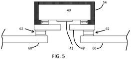
- Figure 5 shows the sensor package soldered to a customer board 60 by solder connections 62.
- the intermediate carrier 52 protects the sensor elements during the customer soldering operation. In particular it provides tolerance to the quality of cleaning or other processing steps carried out by the customer, so that the connection of the sensor chip to the customer PCB is more reliable and easier to perform.
- This example thus provides a near-CSP package which uses an intermediate carrier, which can be a laminate structure, and uses non-solder bumps as the interconnection between the chip and the intermediate carrier.
- an intermediate carrier which can be a laminate structure
- non-solder bumps as the interconnection between the chip and the intermediate carrier.
- the solder is replaced by metal bumps (such as gold, nickel gold, copper or other metals) and the connection between the chip and the intermediate carrier is made using an adhesive.
- sensors configured to detect various different variations in environmental parameters such as light, humidity, gas or liquid concentrations or pressure.
- the chip and the package are typically square or rectangular.
- Gold, gold nickel and copper bumps have been given as examples above.
- the most common example for this type of connection is gold bumps. Copper can be used, but there is a risk of oxidation. Electroless nickel or nickel gold bumps can also be considered.
- the intermediate carrier essentially can comprise a printed circuit board structure, namely a laminate construction.
- the materials may be different to a conventional PCB.
- a BT (Bismaleimide-Triazine resin) laminate can for example be used, using a glass woven material core.
- Vertical interconnects can be formed in the laminate by drilled vias.
- the same type of construction can be made with ceramics, for example a multilayer ceramic (using alumina or glass ceramic stacks that are sintered together).
- One chip may carry a single sensor, although more than one sensor is common.
- a sensor device may even include an array of individual sensor electrodes.
- the package size is typically in the range of 1mm 2 to 10mm 2 . Typical sizes are thus in the range 1x1 mm to 3x3 mm.
- the overmoudling compound can be an epoxy based molding compound. Silicon based molding compounds can also be used.
- the opening in the carrier can be much smaller than the sensor electrode area.
- it can have a linear dimension of less than 200um, for example around 100um.
- the sensor package can be part of a sensor system, for example analytical equipment. It may also be provided as an additional function to another product such as a mobile phone.
- a sensor system for example analytical equipment.
- pressure sensors are known for use as barometers within mobile phones, to provide altitude information to obtain a faster GPS coordinate fix.
- a microphone is also essentially a pressure sensor.
- the amount of space occupied by the sensor needs to be as low as possible when it is to be incorporated into a small product, and thus the reduction of floorspace enabled is of interest.
Landscapes
- Physics & Mathematics (AREA)
- General Physics & Mathematics (AREA)
- Pressure Sensors (AREA)
- Wire Bonding (AREA)
- Engineering & Computer Science (AREA)
- Microelectronics & Electronic Packaging (AREA)
- Measuring Fluid Pressure (AREA)
Description
- This application relates to sensor chip packages.
- Quad flat packages are one example of surface mount integrated circuit package, in which gull wing leads extend from each of the four sides of the package. A modification which is aimed at providing improved miniaturisation, and which has been proposed for sensor packages, is a so-called Heatsink Very-thin Quad Flat-pack No-leads package (HVQFN). This is a package with no component leads extending from the package, and in which the package includes an integrated heat sink part. The package is for mounting on a printed circuit board by soldering, with other surface mount devices.
-
Figure 1(a) shows a HVQFN package for soldering onto a PCB. Thesensor chip 10 haspads 11 around the outer region of the top surface. In one example these pads connect tobond wires 14 which extend down to acarrier 12 such as a lead frame, which provides a fan out function. The bond wires are embedded in the package. The bond wires are connected by means of wirebonding. This is usually a "cold welding" process in the sense that the materials that are joined are not brought into the liquid state (as in real welding and soldering processes). A metallization is present on the bond pads when an IC is intended for wirebonding, and this is often aluminum or gold. - The
lead frame 12 has outer contacts which are soldered to anunderlying PCB 13, and a central die pad area beneath thechip 10. The central die pad area is also soldered to the PCB, and this solder region performs a heat sink function. - Instead of a lead frame, the carrier can for example be a laminate substrate.
- The
chip 10 carries one ormore sensor elements 16. A HVQFN cavity package allows for the sensors on the chip to have an open access to the environment by providing package encapsulation with an opening through which the sensor area is exposed. -
Figure 1(b) shows a sensor chip withsolder bumps 18 on thepads 11 which could be used to enable the chip to be mounted directly onto a PCB. A disadvantage of the package ofFigure 1(a) is that the package size is relatively large compared to the die size, as represented byarrows 20. - It is clear that a chip scale package (CSP) would be preferred from a size and cost point of view, for example by directly soldering the chip to a PCB.
- However, the disadvantage of this approach for sensors is the risk of contamination from the CSP process, in particular the risk of solder splatter when solder bumps are reflow soldered when those solder bumps are attached at the wafer level, but also during the board soldering process at the customer side which might pollute the sensor area, and affect its functionality.
-
Figures 2 and 3 are used to illustrate the problems of soldering the chip directly to a PCB. -
Figure 2 shows how thesensor element 16 can be polluted by the CSP process when being prepared for soldering to a PCB, in particular when forming thesolder balls 18. The process starts with a wafer, on which thebond pads 11 are formed, followed by an under bump metallisation. The solder balls are applied by a reflow process, which can give rise to the pollutant shown as 22. - The resulting package is then soldered at the customer side (i.e. a producer of electronic circuits rather than the individual components) to a
PCB 13. The designer of the chip cannot know what level of cleaning will be applied at this stage, nor the quality of the solder paste and other materials used. -
Figure 3 shows how thesensor element 16 can be polluted by the solder reflow process when the package is mounted on thecustomer circuit board 13. The pollutant is shown as 26. - Document
US 2007/069354 A1 relates to a sensor device with a rigid injection-molding frame surrounding a cavity, the cavity being closed off by a housing bottom. In the cavity, a sensor chip is embedded in a soft rubber-elastic plastic composition. Contact areas of the chip are electrically connected to elastic flip-chip contacts and conductors are arranged on the housing bottom and electrically connected to the elastic flip-chip contacts. Rubber-elastic plastic humps are arranged on the chip to support the flip-chip contacts and ensure their elasticity. The sensor device has a housing bottom opening to improve the coupling of the sensor region to the surroundings. - Document
WO 2008/089969 A2 relates to an electronic device comprising a MEMS device with a differential sensor, which is attached to a substrate. The substrate is provided with a passing opening and the MEMS device is aligned with the passing opening, so that the sensitive portion of the differential sensor is exposed to the environment. A protective package incorporates at least partially the MEMS device and the substrate. - Document
US 2006/055061 A1 relates to a semiconductor device comprising a substrate with an opening and a semiconductor chip attached to a first surface of a substrate by means of an adhesive layer, wherein the semiconductor chip is aligned with the opening of the substrate. Chip bonding pads on the semiconductor chip are wire-bonded to substrate bonding pads on a second surface of the substrate. The second surface of the substrate can be attached to a PCB by means of outer connections balls. An encapsulating resin is provided around the semiconductor chip. - Document
US 6 396 116 B1 relates to a sensor package comprising a first substrate with an optical sensor and solder balls, and an intermediate second substrate, which is bonded to the first substrate and has an opening above the sensor element. The contact pads of the two substrates may be electrically connected by a combination of conductive balls and a conductive adhesive. Contact pads and solder balls connect the second substrate with a circuit board. - Document
US 2005/189635 A1 relates to a package for an acoustic transducer chip wherein a chip is electrically connected to a top panel through soldered interconnects. The interconnects are connected through the top panel to a plurality of contacts, which are connected by solder balls to terminals of a circuit panel. An acoustic port is aligned with an opening of the circuit panel. - Document
JP 2012 098234 A - There is therefore a need for a sensor package which protects the sensor elements but which uses less space than the wire bond package of
Figure 1(a) . - The invention is defined by the claims.
- According to an example, there is provided a sensor package, comprising:
- an integrated circuit chip which carries at least one sensor element on a first surface;
- an intermediate carrier having a first surface to which the first surface of the integrated circuit chip is bonded by an adhesive, wherein the intermediate carrier has an opening beneath the sensor element; and
- solder bond pads on a second surface of the intermediate carrier opposite the first surface.
- The adhesive bonding avoids contamination from solder related processes when forming the package. The intermediate carrier provides protection for the sensor elements on the chip.
- The package can be formed as a "near-CSP" (chip scale package) in that intermediate carrier area does not need to be significantly larger than the chip. The package uses an intermediate carrier with adhesive interconnects between the chip and the intermediate carrier.
- For example, the outer shape defined by the outer edge of the intermediate carrier is preferably within 0.5mm of the outer edge of the shape of the chip, more preferably within 0.4mm and even more preferably within 0.3mm.
- This is possible because no space is required for wire bonds, for example. Despite the small package size, the intermediate carrier with a sensor opening provides protection for the sensor when soldering the package to a customer PCB.
- The integrated circuit chip can comprise gold bumps or Nickel gold bumps (i.e. electroless nickel bumps with a tiny gold protection layer to avoid oxidation), which are bonded to the first surface of the intermediate carrier by the adhesive. This is one way to avoid the use of soldering in the package manufacture.
- The adhesive can comprise an anisotropic conductive glue or a non-conductive glue.
- The opening has a smaller area than the sensor area of the sensor element. In this way, the intermediate carrier acts as a barrier to protect the sensor, and only an opening large enough for the correct sensor operation is needed.
- An overmoulding can optionally be provided over the integrated circuit chip to improve the robustness of the package.
- A sensor device can comprise a circuit board and a sensor package, fixed to the circuit board by soldering of the solder bond pad to tracks on the circuit board.
- An example also provides a method of manufacturing a sensor package, comprising:
- providing an integrated circuit chip which carries at least one sensor element on a first surface; and
- bonding the first surface of the integrated circuit chip to a first surface of an intermediate carrier using an adhesive, wherein the intermediate carrier has an opening beneath the sensor element,
- wherein the intermediate carrier comprises solder bond pads on a second surface of the intermediate carrier opposite the fist surface.
- Examples will now be described in detail with reference to the accompanying drawings, in which:
-
Figure 1 shows a known HVQFN sensor package as well as a basic chip package to enable a size comparison; -
Figure 2 shows a first contamination problem that can arise when a sensor chip is directly attached to a PCB; -
Figure 3 shows a second contamination problem that can arise when a sensor chip is directly attached to a PCB; -
Figure 4 shows an example of package and method for forming the package; and -
Figure 5 shows the package ofFigure 4 attached to a circuit board. - This application relates to a sensor package with which a sensor chip is bonded to an intermediate carrier, with the sensor element above an opening or a set of openings in the carrier.
- The package is for soldering to a board, during which the intermediate carrier protects the sensor part of the sensor chip.
-
Figure 4 shows a method of manufacturing a sensor package. - The method starts with the
integrated circuit chip 40 which carries at least onesensor element 42 on afirst surface 41. The first surface also carries metal bumps 44, for example of gold or Nickel gold or copper. These are each formed over a metal pad which defines the final input or output terminal of the chip, and an under bump metallisation layer is between the metal pad and the metal bump. - The
first surface 41 of theintegrated circuit chip 40 is bonded to a first surface of anintermediate carrier 48 using an adhesive, such as an anisotropic conductive adhesive (ACA) or a non conductive adhesive (NCA). The adhesive can be applied in the form of a tape or a paste. Theintermediate carrier 48 has anopening 50 or a set of openings beneath thesensor element 42. - Note that there is generally no need for the sensor element sensor surface to be aligned with the opening. For example, the sensor may be a pressure sensor for which alignment is not required. Similarly, for chemical sensors, there is no need for direct alignment.
- The
intermediate carrier 48 comprisessolder bond pads 52 on a second surface of the intermediate carrier opposite the first surface. These are provided so that the overall package can be mounted on a printed circuit board as a surface mount device, simultaneously with the mounting of other surface mount components. - The area of the integrated circuit chip can for example be at least 60% of the area of the shape defined by the outer edge of the
intermediate carrier 48, so that a near chip scale package is produced. The area can be at least 70% or even at least 80% of the carrier area. - Similarly, the outer shape defined by the outer edge of the intermediate carrier can be within 0.5mm of the outer edge of the shape of the chip, more preferably within 0.4mm and even more preferably within 0.3mm. Again, this means the package size can be close to the chip size to assist miniaturisation and reduction of cost.
- The
opening 50 or set of openings have a smaller area than the sensor area of thesensor element 42, and the intermediate carrier acts as a shield to protect thesensor element 42. Theopening 50 can be as small as possible while allowing the sensor functionality. - The chip can then be overmoulded with a
resin 54 to define the package. - The intermediate carrier can comprise a laminate structure, and it provides the required electrical connections between the sensor chip terminals and the
bond pads 52. -
Figure 5 shows the sensor package soldered to acustomer board 60 bysolder connections 62. Theintermediate carrier 52 protects the sensor elements during the customer soldering operation. In particular it provides tolerance to the quality of cleaning or other processing steps carried out by the customer, so that the connection of the sensor chip to the customer PCB is more reliable and easier to perform. - This example thus provides a near-CSP package which uses an intermediate carrier, which can be a laminate structure, and uses non-solder bumps as the interconnection between the chip and the intermediate carrier. In particular, to avoid contamination from CSP-processing, the solder is replaced by metal bumps (such as gold, nickel gold, copper or other metals) and the connection between the chip and the intermediate carrier is made using an adhesive.
- These examples can be applied to sensors configured to detect various different variations in environmental parameters such as light, humidity, gas or liquid concentrations or pressure.
- The chip and the package are typically square or rectangular.
- Gold, gold nickel and copper bumps have been given as examples above. In combination with an adhesive, the most common example for this type of connection is gold bumps. Copper can be used, but there is a risk of oxidation. Electroless nickel or nickel gold bumps can also be considered.
- The intermediate carrier essentially can comprise a printed circuit board structure, namely a laminate construction. The materials may be different to a conventional PCB. A BT (Bismaleimide-Triazine resin) laminate can for example be used, using a glass woven material core. Vertical interconnects can be formed in the laminate by drilled vias.
- The same type of construction can be made with ceramics, for example a multilayer ceramic (using alumina or glass ceramic stacks that are sintered together).
- One chip may carry a single sensor, although more than one sensor is common. A sensor device may even include an array of individual sensor electrodes.
- The package size is typically in the range of 1mm2 to 10mm2. Typical sizes are thus in the range 1x1 mm to 3x3 mm.
- The overmoudling compound can be an epoxy based molding compound. Silicon based molding compounds can also be used.
- The opening in the carrier can be much smaller than the sensor electrode area. For example, it can have a linear dimension of less than 200um, for example around 100um.
- The sensor package can be part of a sensor system, for example analytical equipment. It may also be provided as an additional function to another product such as a mobile phone. For example, pressure sensors are known for use as barometers within mobile phones, to provide altitude information to obtain a faster GPS coordinate fix. A microphone is also essentially a pressure sensor. Thus, the amount of space occupied by the sensor needs to be as low as possible when it is to be incorporated into a small product, and thus the reduction of floorspace enabled is of interest.
- Other variations to the disclosed embodiments can be understood and effected by those skilled in the art in practicing the claimed invention, from a study of the drawings, the disclosure, and the appended claims. In the claims, the word "comprising" does not exclude other elements or steps, and the indefinite article "a" or "an" does not exclude a plurality. The mere fact that certain measures are recited in mutually different dependent claims does not indicate that a combination of these measured cannot be used to advantage. Any reference signs in the claims should not be construed as limiting the scope.
Claims (11)
- A sensor package, comprising:an integrated circuit chip (40) which carries at least one sensor element (42) on a first surface and comprises non-solder metal bumps (44), in particular comprises gold bumps, nickel bumps or gold-nickel bumps;an intermediate carrier (48) having a first surface to which the first surface of the integrated circuit chip is bonded by an adhesive, wherein the intermediate carrier has a set of openings (50) comprising at least one opening (50) beneath the sensor element (42) and wherein the metal bumps (44) are bonded to the first surface of the intermediate carrier (48) by the adhesive; andsolder bond pads (52) on a second surface of the intermediate carrier (48) opposite the fist surface,wherein the outer shape defined by the outer edge of the intermediate carrier is within 0.5 mm of the outer edge of the shape of the chip,wherein the intermediate carrier (48) forms a shield to protect the sensor element (42) when soldering the sensor package to a circuit board (60), andwherein the set of openings (50) has a smaller area than a sensor area of the sensor element (42).
- A package as claimed in claim 1, wherein the outer shape defined by the outer edge of the intermediate carrier is within 0.4 mm of the outer edge of the shape of the chip.
- A package as claimed in claim 1, wherein the outer shape defined by the outer edge of the intermediate carrier is within 0.3 mm of the outer edge of the shape of the chip.
- A package as claimed in claim 1, wherein the intermediate carrier (48) comprises a laminate structure or a ceramics providing electrical connections between the integrated circuit chip (40) and the solder bond pads (52).
- A package as claimed in claim 1, wherein the adhesive comprises an anisotropic conductive glue or a non-conductive glue.
- A sensor device, comprising:a circuit board (60); anda sensor package as claimed in claim 1, fixed to the circuit board by soldering of the solder bond pads (52) to tracks on the circuit board (60).
- A method of manufacturing a sensor package, comprising:providing an integrated circuit chip (40) which carries at least one sensor element (42) on a first surface; andbonding the first surface of the integrated circuit chip (40) to a first surface of an intermediate carrier (48) by bonding non-solder metal bumps (44), in particular gold bumps, nickel bumps or gold-nickel bumps, of the integrated circuit chip (40) to the first surface of the intermediate carrier (48) using an adhesive, wherein the intermediate carrier has a set of openings (50) comprising at least one opening (50) beneath the sensor element,wherein the intermediate carrier (48) comprises solder bond pads (52) on a second surface of the intermediate carrier opposite the first surface,wherein the outer shape defined by the outer edge of the intermediate carrier is within 0.5 mm of the outer edge of the shape of the chip,wherein the intermediate carrier (48) forms a shield to protect the sensor element (42) when soldering the sensor package to a circuit board (60), andwherein the set of openings (50) has a smaller area than a sensor area of the sensor element (42).
- A method as claimed in claim 7, wherein the outer shape defined by the outer edge of the intermediate carrier is within 0.4 mm of the outer edge of the shape of the chip.
- A method as claimed in claim 7, wherein the outer shape defined by the outer edge of the intermediate carrier is within 0.3 mm of the outer edge of the shape of the chip.
- A method as claimed in claim 7, wherein the intermediate carrier comprises a laminate structure or a ceramics providing electrical connections between the integrated circuit chip (40) and the solder bond pads (52).
- A method as claimed in claim 7, further comprising soldering the solder bond pads to tracks of a circuit board.
Priority Applications (4)
| Application Number | Priority Date | Filing Date | Title |
|---|---|---|---|
| EP13196851.3A EP2884242B1 (en) | 2013-12-12 | 2013-12-12 | Sensor Package And Manufacturing Method |
| CN201410662747.3A CN104716115A (en) | 2013-12-12 | 2014-11-19 | Sensor package and manufacturing method thereof |
| CN201910757601.XA CN110459520A (en) | 2013-12-12 | 2014-11-19 | Sensor package and method of making the same |
| US14/566,309 US10192842B2 (en) | 2013-12-12 | 2014-12-10 | Package for environmental parameter sensors and method for manufacturing a package for environmental parameter sensors |
Applications Claiming Priority (1)
| Application Number | Priority Date | Filing Date | Title |
|---|---|---|---|
| EP13196851.3A EP2884242B1 (en) | 2013-12-12 | 2013-12-12 | Sensor Package And Manufacturing Method |
Publications (2)
| Publication Number | Publication Date |
|---|---|
| EP2884242A1 EP2884242A1 (en) | 2015-06-17 |
| EP2884242B1 true EP2884242B1 (en) | 2021-12-08 |
Family
ID=49916813
Family Applications (1)
| Application Number | Title | Priority Date | Filing Date |
|---|---|---|---|
| EP13196851.3A Not-in-force EP2884242B1 (en) | 2013-12-12 | 2013-12-12 | Sensor Package And Manufacturing Method |
Country Status (3)
| Country | Link |
|---|---|
| US (1) | US10192842B2 (en) |
| EP (1) | EP2884242B1 (en) |
| CN (2) | CN110459520A (en) |
Families Citing this family (3)
| Publication number | Priority date | Publication date | Assignee | Title |
|---|---|---|---|---|
| EP3260821B1 (en) | 2016-06-21 | 2019-09-11 | ams International AG | Sensor package and method of producing the sensor package |
| NL2017885B1 (en) * | 2016-11-29 | 2018-06-11 | Sencio B V | Sensor package and method of manufacturing the same |
| DE102017212748B4 (en) * | 2017-07-25 | 2021-02-11 | Infineon Technologies Ag | Sensor devices and methods of making them |
Citations (3)
| Publication number | Priority date | Publication date | Assignee | Title |
|---|---|---|---|---|
| US6396116B1 (en) * | 2000-02-25 | 2002-05-28 | Agilent Technologies, Inc. | Integrated circuit packaging for optical sensor devices |
| US20050189635A1 (en) * | 2004-03-01 | 2005-09-01 | Tessera, Inc. | Packaged acoustic and electromagnetic transducer chips |
| JP2012098234A (en) * | 2010-11-05 | 2012-05-24 | Figaro Eng Inc | Gas sensor |
Family Cites Families (32)
| Publication number | Priority date | Publication date | Assignee | Title |
|---|---|---|---|---|
| US6140144A (en) * | 1996-08-08 | 2000-10-31 | Integrated Sensing Systems, Inc. | Method for packaging microsensors |
| FR2798226B1 (en) * | 1999-09-02 | 2002-04-05 | St Microelectronics Sa | METHOD FOR PACKAGING A SEMICONDUCTOR CHIP CONTAINING SENSORS AND PACKAGE OBTAINED |
| US7247938B2 (en) * | 2002-04-11 | 2007-07-24 | Nxp B.V. | Carrier, method of manufacturing a carrier and an electronic device |
| US7323772B2 (en) * | 2002-08-28 | 2008-01-29 | Micron Technology, Inc. | Ball grid array structures and tape-based method of manufacturing same |
| JP2004179232A (en) * | 2002-11-25 | 2004-06-24 | Seiko Epson Corp | Semiconductor device, method of manufacturing the same, and electronic device |
| JP4069771B2 (en) * | 2003-03-17 | 2008-04-02 | セイコーエプソン株式会社 | SEMICONDUCTOR DEVICE, ELECTRONIC DEVICE, AND SEMICONDUCTOR DEVICE MANUFACTURING METHOD |
| US6995462B2 (en) * | 2003-09-17 | 2006-02-07 | Micron Technology, Inc. | Image sensor packages |
| US7368695B2 (en) * | 2004-05-03 | 2008-05-06 | Tessera, Inc. | Image sensor package and fabrication method |
| JP2006073825A (en) * | 2004-09-02 | 2006-03-16 | Toshiba Corp | Semiconductor device and mounting method thereof |
| TWM264651U (en) * | 2004-10-21 | 2005-05-11 | Chipmos Technologies Inc | Package structure of image sensor device |
| TWI250625B (en) * | 2004-12-27 | 2006-03-01 | Advanced Semiconductor Eng | Image sensor module package |
| US7635910B2 (en) | 2005-01-20 | 2009-12-22 | Infineon Technologies Ag | Semiconductor package and method |
| DE102005046008B4 (en) * | 2005-09-26 | 2007-05-24 | Infineon Technologies Ag | Semiconductor sensor component with sensor chip and method for producing the same |
| KR100746330B1 (en) * | 2005-11-24 | 2007-08-03 | 한국과학기술원 | Connection method between electronic parts using ultrasonic wave |
| US8159825B1 (en) * | 2006-08-25 | 2012-04-17 | Hypres Inc. | Method for fabrication of electrical contacts to superconducting circuits |
| CN101512765A (en) * | 2006-09-15 | 2009-08-19 | 富士通微电子株式会社 | Semiconductor device and method for manufacturing the same |
| ITMI20070099A1 (en) * | 2007-01-24 | 2008-07-25 | St Microelectronics Srl | ELECTRONIC DEVICE INCLUDING DIFFERENTIAL SENSOR DEVICES MEMS AND SUBSTRATES LAUNDRY |
| US7607355B2 (en) * | 2007-02-16 | 2009-10-27 | Yamaha Corporation | Semiconductor device |
| JP2008218643A (en) | 2007-03-02 | 2008-09-18 | Fujitsu Ltd | Semiconductor device and manufacturing method thereof |
| JP2008227137A (en) * | 2007-03-13 | 2008-09-25 | Matsushita Electric Ind Co Ltd | Electrostatic countermeasure component and light emitting diode module using the same |
| US20090183999A1 (en) * | 2008-01-18 | 2009-07-23 | Alfredo Ibarra | Gas sensor element and method |
| US7692313B2 (en) * | 2008-03-04 | 2010-04-06 | Powertech Technology Inc. | Substrate and semiconductor package for lessening warpage |
| WO2013167466A2 (en) | 2012-05-11 | 2013-11-14 | Nxp B.V. | Integrated circuit with directional light sensor, device including such an ic and method of manufacturing such an ic |
| EP2693207A1 (en) | 2012-07-30 | 2014-02-05 | Nxp B.V. | Integrated circuit comprising a capacitive gas sensor |
| EP2708878B1 (en) | 2012-09-12 | 2020-04-22 | ams international AG | Method of manufacturing an integrated circuit comprising a gas sensor |
| EP2720034B1 (en) | 2012-10-12 | 2016-04-27 | ams International AG | Integrated Circuit comprising a relative humidity sensor and a thermal conductivity based gas sensor |
| EP2743691A1 (en) | 2012-12-14 | 2014-06-18 | Nxp B.V. | Detection of an acidic (CO2, SO2) or basic (NH3) gas by monitoring a dielectric relaxation of a reaction product (for example of a zwitterion) of an acid-base reaction of the gas with a chemical compound (like DBU) using an integrated circuit |
| EP2743677A1 (en) | 2012-12-14 | 2014-06-18 | Nxp B.V. | IR COx sensor and integrated circuit comprising the same |
| EP2752660B1 (en) | 2013-01-07 | 2016-08-31 | Nxp B.V. | Integrated circuit comprising an optical CO2 sensor and manufacturing method |
| EP2759832B1 (en) | 2013-01-23 | 2020-11-11 | Sciosense B.V. | Electrochemical sensor device |
| US9177903B2 (en) * | 2013-03-29 | 2015-11-03 | Stmicroelectronics, Inc. | Enhanced flip-chip die architecture |
| EP2793018A1 (en) | 2013-04-19 | 2014-10-22 | Nxp B.V. | Thermal conductivity based gas sensor |
-
2013
- 2013-12-12 EP EP13196851.3A patent/EP2884242B1/en not_active Not-in-force
-
2014
- 2014-11-19 CN CN201910757601.XA patent/CN110459520A/en active Pending
- 2014-11-19 CN CN201410662747.3A patent/CN104716115A/en active Pending
- 2014-12-10 US US14/566,309 patent/US10192842B2/en active Active
Patent Citations (3)
| Publication number | Priority date | Publication date | Assignee | Title |
|---|---|---|---|---|
| US6396116B1 (en) * | 2000-02-25 | 2002-05-28 | Agilent Technologies, Inc. | Integrated circuit packaging for optical sensor devices |
| US20050189635A1 (en) * | 2004-03-01 | 2005-09-01 | Tessera, Inc. | Packaged acoustic and electromagnetic transducer chips |
| JP2012098234A (en) * | 2010-11-05 | 2012-05-24 | Figaro Eng Inc | Gas sensor |
Also Published As
| Publication number | Publication date |
|---|---|
| EP2884242A1 (en) | 2015-06-17 |
| CN104716115A (en) | 2015-06-17 |
| US10192842B2 (en) | 2019-01-29 |
| US20150171042A1 (en) | 2015-06-18 |
| CN110459520A (en) | 2019-11-15 |
Similar Documents
| Publication | Publication Date | Title |
|---|---|---|
| JP4926380B2 (en) | Integrated circuit device and electrical assembly | |
| US8569082B2 (en) | Semiconductor package with a mold material encapsulating a chip and a portion of a lead frame | |
| CN100499052C (en) | Planar grid array packaging device and manufacturing method thereof | |
| CN102257614B (en) | Comprise the sensing of the opposite side being arranged on base plate for packaging and the integrated sensor of process tube core | |
| US8487424B2 (en) | Routable array metal integrated circuit package fabricated using partial etching process | |
| CN107230643B (en) | Packaging device with extension structure for forming opening in encapsulation body | |
| US20140329362A1 (en) | QFN/SON-Compatible Package | |
| CN102270589B (en) | The manufacture method of semiconductor element and corresponding semiconductor element | |
| US8994157B1 (en) | Circuit system in a package | |
| CN109417081B (en) | Chip packaging structure, method and electronic equipment | |
| US8274797B2 (en) | Electronic component | |
| CN112864022B (en) | Manufacturing method of packaging structure and packaging structure | |
| US10192842B2 (en) | Package for environmental parameter sensors and method for manufacturing a package for environmental parameter sensors | |
| US6700190B2 (en) | Integrated circuit device with exposed upper and lower die surfaces | |
| CN106960824A (en) | Capping structure and semiconductor device package including the same | |
| US8344500B2 (en) | Integrated circuit package module and method of the same | |
| KR20080074468A (en) | Surface Mounting Method of Semiconductor Chip Using Ultrasonic Wave | |
| KR100207902B1 (en) | Multi chip package using lead frame | |
| CN210040172U (en) | Chip packaging structure and electronic equipment | |
| TWI491001B (en) | Integrated circuit assembly | |
| KR101204741B1 (en) | Semiconductor package including heat sink and manufacturing process thereof | |
| CN120829141A (en) | Pressure sensors and electronic equipment | |
| CN113964098A (en) | Semiconductor device and method for manufacturing the same | |
| KR20070079654A (en) | Printed circuit board for flip chip bonding and manufacturing method of ball grid array package using the same | |
| US20080099927A1 (en) | semiconductor package manufacturing method and semiconductor apparatus |
Legal Events
| Date | Code | Title | Description |
|---|---|---|---|
| PUAI | Public reference made under article 153(3) epc to a published international application that has entered the european phase |
Free format text: ORIGINAL CODE: 0009012 |
|
| 17P | Request for examination filed |
Effective date: 20140326 |
|
| AK | Designated contracting states |
Kind code of ref document: A1 Designated state(s): AL AT BE BG CH CY CZ DE DK EE ES FI FR GB GR HR HU IE IS IT LI LT LU LV MC MK MT NL NO PL PT RO RS SE SI SK SM TR |
|
| AX | Request for extension of the european patent |
Extension state: BA ME |
|
| RAP1 | Party data changed (applicant data changed or rights of an application transferred) |
Owner name: AMS INTERNATIONAL AG |
|
| RBV | Designated contracting states (corrected) |
Designated state(s): AL AT BE BG CH CY CZ DE DK EE ES FI FR GB GR HR HU IE IS IT LI LT LU LV MC MK MT NL NO PL PT RO RS SE SI SK SM TR |
|
| STAA | Information on the status of an ep patent application or granted ep patent |
Free format text: STATUS: EXAMINATION IS IN PROGRESS |
|
| 17Q | First examination report despatched |
Effective date: 20180507 |
|
| RAP1 | Party data changed (applicant data changed or rights of an application transferred) |
Owner name: AMS INTERNATIONAL AG |
|
| GRAP | Despatch of communication of intention to grant a patent |
Free format text: ORIGINAL CODE: EPIDOSNIGR1 |
|
| STAA | Information on the status of an ep patent application or granted ep patent |
Free format text: STATUS: GRANT OF PATENT IS INTENDED |
|
| INTG | Intention to grant announced |
Effective date: 20210706 |
|
| GRAS | Grant fee paid |
Free format text: ORIGINAL CODE: EPIDOSNIGR3 |
|
| GRAA | (expected) grant |
Free format text: ORIGINAL CODE: 0009210 |
|
| GRAF | Information related to payment of grant fee modified |
Free format text: ORIGINAL CODE: EPIDOSCIGR3 |
|
| STAA | Information on the status of an ep patent application or granted ep patent |
Free format text: STATUS: THE PATENT HAS BEEN GRANTED |
|
| AK | Designated contracting states |
Kind code of ref document: B1 Designated state(s): AL AT BE BG CH CY CZ DE DK EE ES FI FR GB GR HR HU IE IS IT LI LT LU LV MC MK MT NL NO PL PT RO RS SE SI SK SM TR |
|
| REG | Reference to a national code |
Ref country code: GB Ref legal event code: FG4D |
|
| REG | Reference to a national code |
Ref country code: AT Ref legal event code: REF Ref document number: 1454103 Country of ref document: AT Kind code of ref document: T Effective date: 20211215 Ref country code: CH Ref legal event code: EP |
|
| REG | Reference to a national code |
Ref country code: DE Ref legal event code: R096 Ref document number: 602013080325 Country of ref document: DE |
|
| REG | Reference to a national code |
Ref country code: IE Ref legal event code: FG4D |
|
| REG | Reference to a national code |
Ref country code: LT Ref legal event code: MG9D |
|
| REG | Reference to a national code |
Ref country code: NL Ref legal event code: MP Effective date: 20211208 |
|
| PG25 | Lapsed in a contracting state [announced via postgrant information from national office to epo] |
Ref country code: RS Free format text: LAPSE BECAUSE OF FAILURE TO SUBMIT A TRANSLATION OF THE DESCRIPTION OR TO PAY THE FEE WITHIN THE PRESCRIBED TIME-LIMIT Effective date: 20211208 Ref country code: LT Free format text: LAPSE BECAUSE OF FAILURE TO SUBMIT A TRANSLATION OF THE DESCRIPTION OR TO PAY THE FEE WITHIN THE PRESCRIBED TIME-LIMIT Effective date: 20211208 Ref country code: FI Free format text: LAPSE BECAUSE OF FAILURE TO SUBMIT A TRANSLATION OF THE DESCRIPTION OR TO PAY THE FEE WITHIN THE PRESCRIBED TIME-LIMIT Effective date: 20211208 Ref country code: BG Free format text: LAPSE BECAUSE OF FAILURE TO SUBMIT A TRANSLATION OF THE DESCRIPTION OR TO PAY THE FEE WITHIN THE PRESCRIBED TIME-LIMIT Effective date: 20220308 |
|
| PGFP | Annual fee paid to national office [announced via postgrant information from national office to epo] |
Ref country code: GB Payment date: 20220119 Year of fee payment: 9 Ref country code: DE Payment date: 20220119 Year of fee payment: 9 |
|
| REG | Reference to a national code |
Ref country code: AT Ref legal event code: MK05 Ref document number: 1454103 Country of ref document: AT Kind code of ref document: T Effective date: 20211208 |
|
| PG25 | Lapsed in a contracting state [announced via postgrant information from national office to epo] |
Ref country code: SE Free format text: LAPSE BECAUSE OF FAILURE TO SUBMIT A TRANSLATION OF THE DESCRIPTION OR TO PAY THE FEE WITHIN THE PRESCRIBED TIME-LIMIT Effective date: 20211208 Ref country code: NO Free format text: LAPSE BECAUSE OF FAILURE TO SUBMIT A TRANSLATION OF THE DESCRIPTION OR TO PAY THE FEE WITHIN THE PRESCRIBED TIME-LIMIT Effective date: 20220308 Ref country code: LV Free format text: LAPSE BECAUSE OF FAILURE TO SUBMIT A TRANSLATION OF THE DESCRIPTION OR TO PAY THE FEE WITHIN THE PRESCRIBED TIME-LIMIT Effective date: 20211208 Ref country code: HR Free format text: LAPSE BECAUSE OF FAILURE TO SUBMIT A TRANSLATION OF THE DESCRIPTION OR TO PAY THE FEE WITHIN THE PRESCRIBED TIME-LIMIT Effective date: 20211208 Ref country code: GR Free format text: LAPSE BECAUSE OF FAILURE TO SUBMIT A TRANSLATION OF THE DESCRIPTION OR TO PAY THE FEE WITHIN THE PRESCRIBED TIME-LIMIT Effective date: 20220309 Ref country code: ES Free format text: LAPSE BECAUSE OF FAILURE TO SUBMIT A TRANSLATION OF THE DESCRIPTION OR TO PAY THE FEE WITHIN THE PRESCRIBED TIME-LIMIT Effective date: 20211208 |
|
| PG25 | Lapsed in a contracting state [announced via postgrant information from national office to epo] |
Ref country code: NL Free format text: LAPSE BECAUSE OF FAILURE TO SUBMIT A TRANSLATION OF THE DESCRIPTION OR TO PAY THE FEE WITHIN THE PRESCRIBED TIME-LIMIT Effective date: 20211208 |
|
| PG25 | Lapsed in a contracting state [announced via postgrant information from national office to epo] |
Ref country code: SM Free format text: LAPSE BECAUSE OF FAILURE TO SUBMIT A TRANSLATION OF THE DESCRIPTION OR TO PAY THE FEE WITHIN THE PRESCRIBED TIME-LIMIT Effective date: 20211208 Ref country code: SK Free format text: LAPSE BECAUSE OF FAILURE TO SUBMIT A TRANSLATION OF THE DESCRIPTION OR TO PAY THE FEE WITHIN THE PRESCRIBED TIME-LIMIT Effective date: 20211208 Ref country code: RO Free format text: LAPSE BECAUSE OF FAILURE TO SUBMIT A TRANSLATION OF THE DESCRIPTION OR TO PAY THE FEE WITHIN THE PRESCRIBED TIME-LIMIT Effective date: 20211208 Ref country code: PT Free format text: LAPSE BECAUSE OF FAILURE TO SUBMIT A TRANSLATION OF THE DESCRIPTION OR TO PAY THE FEE WITHIN THE PRESCRIBED TIME-LIMIT Effective date: 20220408 Ref country code: EE Free format text: LAPSE BECAUSE OF FAILURE TO SUBMIT A TRANSLATION OF THE DESCRIPTION OR TO PAY THE FEE WITHIN THE PRESCRIBED TIME-LIMIT Effective date: 20211208 Ref country code: CZ Free format text: LAPSE BECAUSE OF FAILURE TO SUBMIT A TRANSLATION OF THE DESCRIPTION OR TO PAY THE FEE WITHIN THE PRESCRIBED TIME-LIMIT Effective date: 20211208 |
|
| REG | Reference to a national code |
Ref country code: CH Ref legal event code: PL |
|
| PG25 | Lapsed in a contracting state [announced via postgrant information from national office to epo] |
Ref country code: PL Free format text: LAPSE BECAUSE OF FAILURE TO SUBMIT A TRANSLATION OF THE DESCRIPTION OR TO PAY THE FEE WITHIN THE PRESCRIBED TIME-LIMIT Effective date: 20211208 Ref country code: AT Free format text: LAPSE BECAUSE OF FAILURE TO SUBMIT A TRANSLATION OF THE DESCRIPTION OR TO PAY THE FEE WITHIN THE PRESCRIBED TIME-LIMIT Effective date: 20211208 |
|
| REG | Reference to a national code |
Ref country code: DE Ref legal event code: R097 Ref document number: 602013080325 Country of ref document: DE |
|
| REG | Reference to a national code |
Ref country code: BE Ref legal event code: MM Effective date: 20211231 |
|
| PG25 | Lapsed in a contracting state [announced via postgrant information from national office to epo] |
Ref country code: MC Free format text: LAPSE BECAUSE OF FAILURE TO SUBMIT A TRANSLATION OF THE DESCRIPTION OR TO PAY THE FEE WITHIN THE PRESCRIBED TIME-LIMIT Effective date: 20211208 Ref country code: IS Free format text: LAPSE BECAUSE OF FAILURE TO SUBMIT A TRANSLATION OF THE DESCRIPTION OR TO PAY THE FEE WITHIN THE PRESCRIBED TIME-LIMIT Effective date: 20220408 |
|
| PLBE | No opposition filed within time limit |
Free format text: ORIGINAL CODE: 0009261 |
|
| STAA | Information on the status of an ep patent application or granted ep patent |
Free format text: STATUS: NO OPPOSITION FILED WITHIN TIME LIMIT |
|
| PG25 | Lapsed in a contracting state [announced via postgrant information from national office to epo] |
Ref country code: LU Free format text: LAPSE BECAUSE OF NON-PAYMENT OF DUE FEES Effective date: 20211212 Ref country code: IE Free format text: LAPSE BECAUSE OF NON-PAYMENT OF DUE FEES Effective date: 20211212 Ref country code: DK Free format text: LAPSE BECAUSE OF FAILURE TO SUBMIT A TRANSLATION OF THE DESCRIPTION OR TO PAY THE FEE WITHIN THE PRESCRIBED TIME-LIMIT Effective date: 20211208 Ref country code: AL Free format text: LAPSE BECAUSE OF FAILURE TO SUBMIT A TRANSLATION OF THE DESCRIPTION OR TO PAY THE FEE WITHIN THE PRESCRIBED TIME-LIMIT Effective date: 20211208 |
|
| 26N | No opposition filed |
Effective date: 20220909 |
|
| PG25 | Lapsed in a contracting state [announced via postgrant information from national office to epo] |
Ref country code: SI Free format text: LAPSE BECAUSE OF FAILURE TO SUBMIT A TRANSLATION OF THE DESCRIPTION OR TO PAY THE FEE WITHIN THE PRESCRIBED TIME-LIMIT Effective date: 20211208 Ref country code: BE Free format text: LAPSE BECAUSE OF NON-PAYMENT OF DUE FEES Effective date: 20211231 |
|
| PG25 | Lapsed in a contracting state [announced via postgrant information from national office to epo] |
Ref country code: LI Free format text: LAPSE BECAUSE OF NON-PAYMENT OF DUE FEES Effective date: 20211231 Ref country code: FR Free format text: LAPSE BECAUSE OF NON-PAYMENT OF DUE FEES Effective date: 20220208 Ref country code: CH Free format text: LAPSE BECAUSE OF NON-PAYMENT OF DUE FEES Effective date: 20211231 |
|
| PG25 | Lapsed in a contracting state [announced via postgrant information from national office to epo] |
Ref country code: IT Free format text: LAPSE BECAUSE OF FAILURE TO SUBMIT A TRANSLATION OF THE DESCRIPTION OR TO PAY THE FEE WITHIN THE PRESCRIBED TIME-LIMIT Effective date: 20211208 Ref country code: HU Free format text: LAPSE BECAUSE OF FAILURE TO SUBMIT A TRANSLATION OF THE DESCRIPTION OR TO PAY THE FEE WITHIN THE PRESCRIBED TIME-LIMIT; INVALID AB INITIO Effective date: 20131212 |
|
| PG25 | Lapsed in a contracting state [announced via postgrant information from national office to epo] |
Ref country code: CY Free format text: LAPSE BECAUSE OF FAILURE TO SUBMIT A TRANSLATION OF THE DESCRIPTION OR TO PAY THE FEE WITHIN THE PRESCRIBED TIME-LIMIT Effective date: 20211208 |
|
| REG | Reference to a national code |
Ref country code: DE Ref legal event code: R119 Ref document number: 602013080325 Country of ref document: DE |
|
| GBPC | Gb: european patent ceased through non-payment of renewal fee |
Effective date: 20221212 |
|
| P01 | Opt-out of the competence of the unified patent court (upc) registered |
Effective date: 20230821 |
|
| PG25 | Lapsed in a contracting state [announced via postgrant information from national office to epo] |
Ref country code: GB Free format text: LAPSE BECAUSE OF NON-PAYMENT OF DUE FEES Effective date: 20221212 Ref country code: DE Free format text: LAPSE BECAUSE OF NON-PAYMENT OF DUE FEES Effective date: 20230701 |
|
| PG25 | Lapsed in a contracting state [announced via postgrant information from national office to epo] |
Ref country code: MK Free format text: LAPSE BECAUSE OF FAILURE TO SUBMIT A TRANSLATION OF THE DESCRIPTION OR TO PAY THE FEE WITHIN THE PRESCRIBED TIME-LIMIT Effective date: 20211208 |
|
| PG25 | Lapsed in a contracting state [announced via postgrant information from national office to epo] |
Ref country code: TR Free format text: LAPSE BECAUSE OF FAILURE TO SUBMIT A TRANSLATION OF THE DESCRIPTION OR TO PAY THE FEE WITHIN THE PRESCRIBED TIME-LIMIT Effective date: 20211208 |
|
| PG25 | Lapsed in a contracting state [announced via postgrant information from national office to epo] |
Ref country code: MT Free format text: LAPSE BECAUSE OF FAILURE TO SUBMIT A TRANSLATION OF THE DESCRIPTION OR TO PAY THE FEE WITHIN THE PRESCRIBED TIME-LIMIT Effective date: 20211208 |