EP2883240B1 - Method and apparatus deposition process synchronization - Google Patents
Method and apparatus deposition process synchronization Download PDFInfo
- Publication number
- EP2883240B1 EP2883240B1 EP13828359.3A EP13828359A EP2883240B1 EP 2883240 B1 EP2883240 B1 EP 2883240B1 EP 13828359 A EP13828359 A EP 13828359A EP 2883240 B1 EP2883240 B1 EP 2883240B1
- Authority
- EP
- European Patent Office
- Prior art keywords
- devices
- control parameters
- chamber
- synchronization controller
- process control
- Prior art date
- Legal status (The legal status is an assumption and is not a legal conclusion. Google has not performed a legal analysis and makes no representation as to the accuracy of the status listed.)
- Active
Links
- 238000000034 method Methods 0.000 title claims description 194
- 238000005137 deposition process Methods 0.000 title claims description 13
- 230000008569 process Effects 0.000 claims description 159
- 239000000758 substrate Substances 0.000 claims description 116
- 238000012545 processing Methods 0.000 claims description 46
- 238000004886 process control Methods 0.000 claims description 44
- 239000000463 material Substances 0.000 claims description 42
- 230000001934 delay Effects 0.000 claims description 29
- NJPPVKZQTLUDBO-UHFFFAOYSA-N novaluron Chemical compound C1=C(Cl)C(OC(F)(F)C(OC(F)(F)F)F)=CC=C1NC(=O)NC(=O)C1=C(F)C=CC=C1F NJPPVKZQTLUDBO-UHFFFAOYSA-N 0.000 description 26
- 238000000151 deposition Methods 0.000 description 24
- 239000004020 conductor Substances 0.000 description 18
- 239000007789 gas Substances 0.000 description 18
- 239000010949 copper Substances 0.000 description 17
- 230000008021 deposition Effects 0.000 description 16
- 150000002500 ions Chemical class 0.000 description 14
- 230000004888 barrier function Effects 0.000 description 12
- 238000004544 sputter deposition Methods 0.000 description 11
- RYGMFSIKBFXOCR-UHFFFAOYSA-N Copper Chemical compound [Cu] RYGMFSIKBFXOCR-UHFFFAOYSA-N 0.000 description 10
- 229910052802 copper Inorganic materials 0.000 description 10
- 238000005240 physical vapour deposition Methods 0.000 description 9
- XKRFYHLGVUSROY-UHFFFAOYSA-N Argon Chemical compound [Ar] XKRFYHLGVUSROY-UHFFFAOYSA-N 0.000 description 8
- 238000004891 communication Methods 0.000 description 5
- 238000005530 etching Methods 0.000 description 5
- VYPSYNLAJGMNEJ-UHFFFAOYSA-N Silicium dioxide Chemical compound O=[Si]=O VYPSYNLAJGMNEJ-UHFFFAOYSA-N 0.000 description 4
- XUIMIQQOPSSXEZ-UHFFFAOYSA-N Silicon Chemical compound [Si] XUIMIQQOPSSXEZ-UHFFFAOYSA-N 0.000 description 4
- 229910052782 aluminium Inorganic materials 0.000 description 4
- XAGFODPZIPBFFR-UHFFFAOYSA-N aluminium Chemical compound [Al] XAGFODPZIPBFFR-UHFFFAOYSA-N 0.000 description 4
- 229910052786 argon Inorganic materials 0.000 description 4
- 239000003989 dielectric material Substances 0.000 description 4
- 229910052751 metal Inorganic materials 0.000 description 4
- 239000002184 metal Substances 0.000 description 4
- 230000004044 response Effects 0.000 description 4
- 239000004065 semiconductor Substances 0.000 description 4
- 229910052710 silicon Inorganic materials 0.000 description 4
- 239000010703 silicon Substances 0.000 description 4
- 229910052814 silicon oxide Inorganic materials 0.000 description 4
- 238000005229 chemical vapour deposition Methods 0.000 description 3
- 230000006870 function Effects 0.000 description 3
- 229910052734 helium Inorganic materials 0.000 description 3
- 239000001307 helium Substances 0.000 description 3
- SWQJXJOGLNCZEY-UHFFFAOYSA-N helium atom Chemical compound [He] SWQJXJOGLNCZEY-UHFFFAOYSA-N 0.000 description 3
- 239000011261 inert gas Substances 0.000 description 3
- 229910052743 krypton Inorganic materials 0.000 description 3
- DNNSSWSSYDEUBZ-UHFFFAOYSA-N krypton atom Chemical compound [Kr] DNNSSWSSYDEUBZ-UHFFFAOYSA-N 0.000 description 3
- 229910052754 neon Inorganic materials 0.000 description 3
- GKAOGPIIYCISHV-UHFFFAOYSA-N neon atom Chemical compound [Ne] GKAOGPIIYCISHV-UHFFFAOYSA-N 0.000 description 3
- 239000013077 target material Substances 0.000 description 3
- 239000010936 titanium Substances 0.000 description 3
- 229910052724 xenon Inorganic materials 0.000 description 3
- FHNFHKCVQCLJFQ-UHFFFAOYSA-N xenon atom Chemical compound [Xe] FHNFHKCVQCLJFQ-UHFFFAOYSA-N 0.000 description 3
- 229910052581 Si3N4 Inorganic materials 0.000 description 2
- 229910000577 Silicon-germanium Inorganic materials 0.000 description 2
- RTAQQCXQSZGOHL-UHFFFAOYSA-N Titanium Chemical compound [Ti] RTAQQCXQSZGOHL-UHFFFAOYSA-N 0.000 description 2
- 230000003213 activating effect Effects 0.000 description 2
- 229910045601 alloy Inorganic materials 0.000 description 2
- 239000000956 alloy Substances 0.000 description 2
- WYEMLYFITZORAB-UHFFFAOYSA-N boscalid Chemical compound C1=CC(Cl)=CC=C1C1=CC=CC=C1NC(=O)C1=CC=CN=C1Cl WYEMLYFITZORAB-UHFFFAOYSA-N 0.000 description 2
- 238000006243 chemical reaction Methods 0.000 description 2
- 230000003247 decreasing effect Effects 0.000 description 2
- 238000013461 design Methods 0.000 description 2
- 230000009977 dual effect Effects 0.000 description 2
- 238000004070 electrodeposition Methods 0.000 description 2
- 238000005401 electroluminescence Methods 0.000 description 2
- 230000005672 electromagnetic field Effects 0.000 description 2
- 239000011521 glass Substances 0.000 description 2
- 229910021645 metal ion Inorganic materials 0.000 description 2
- 238000007747 plating Methods 0.000 description 2
- 230000011664 signaling Effects 0.000 description 2
- HQVNEWCFYHHQES-UHFFFAOYSA-N silicon nitride Chemical compound N12[Si]34N5[Si]62N3[Si]51N64 HQVNEWCFYHHQES-UHFFFAOYSA-N 0.000 description 2
- 238000003860 storage Methods 0.000 description 2
- 229910052715 tantalum Inorganic materials 0.000 description 2
- GUVRBAGPIYLISA-UHFFFAOYSA-N tantalum atom Chemical compound [Ta] GUVRBAGPIYLISA-UHFFFAOYSA-N 0.000 description 2
- 229910052719 titanium Inorganic materials 0.000 description 2
- 229910052721 tungsten Inorganic materials 0.000 description 2
- 239000011800 void material Substances 0.000 description 2
- JPVYNHNXODAKFH-UHFFFAOYSA-N Cu2+ Chemical compound [Cu+2] JPVYNHNXODAKFH-UHFFFAOYSA-N 0.000 description 1
- YCKRFDGAMUMZLT-UHFFFAOYSA-N Fluorine atom Chemical compound [F] YCKRFDGAMUMZLT-UHFFFAOYSA-N 0.000 description 1
- 239000004642 Polyimide Substances 0.000 description 1
- KJTLSVCANCCWHF-UHFFFAOYSA-N Ruthenium Chemical compound [Ru] KJTLSVCANCCWHF-UHFFFAOYSA-N 0.000 description 1
- 229910004156 TaNx Inorganic materials 0.000 description 1
- NRTOMJZYCJJWKI-UHFFFAOYSA-N Titanium nitride Chemical compound [Ti]#N NRTOMJZYCJJWKI-UHFFFAOYSA-N 0.000 description 1
- OWXLRKWPEIAGAT-UHFFFAOYSA-N [Mg].[Cu] Chemical compound [Mg].[Cu] OWXLRKWPEIAGAT-UHFFFAOYSA-N 0.000 description 1
- LEVVHYCKPQWKOP-UHFFFAOYSA-N [Si].[Ge] Chemical compound [Si].[Ge] LEVVHYCKPQWKOP-UHFFFAOYSA-N 0.000 description 1
- 238000009825 accumulation Methods 0.000 description 1
- JRBRVDCKNXZZGH-UHFFFAOYSA-N alumane;copper Chemical compound [AlH3].[Cu] JRBRVDCKNXZZGH-UHFFFAOYSA-N 0.000 description 1
- 238000000137 annealing Methods 0.000 description 1
- 238000000429 assembly Methods 0.000 description 1
- 230000000712 assembly Effects 0.000 description 1
- 239000003990 capacitor Substances 0.000 description 1
- 230000015556 catabolic process Effects 0.000 description 1
- 230000008859 change Effects 0.000 description 1
- 239000010941 cobalt Substances 0.000 description 1
- 229910017052 cobalt Inorganic materials 0.000 description 1
- GUTLYIVDDKVIGB-UHFFFAOYSA-N cobalt atom Chemical compound [Co] GUTLYIVDDKVIGB-UHFFFAOYSA-N 0.000 description 1
- 150000001875 compounds Chemical class 0.000 description 1
- 229910001431 copper ion Inorganic materials 0.000 description 1
- HPDFFVBPXCTEDN-UHFFFAOYSA-N copper manganese Chemical compound [Mn].[Cu] HPDFFVBPXCTEDN-UHFFFAOYSA-N 0.000 description 1
- 230000008878 coupling Effects 0.000 description 1
- 238000010168 coupling process Methods 0.000 description 1
- 238000005859 coupling reaction Methods 0.000 description 1
- 230000001351 cycling effect Effects 0.000 description 1
- 238000006731 degradation reaction Methods 0.000 description 1
- 230000003111 delayed effect Effects 0.000 description 1
- 230000001419 dependent effect Effects 0.000 description 1
- 239000010432 diamond Substances 0.000 description 1
- 230000000694 effects Effects 0.000 description 1
- 229940082150 encore Drugs 0.000 description 1
- 230000003090 exacerbative effect Effects 0.000 description 1
- 230000002349 favourable effect Effects 0.000 description 1
- 238000007667 floating Methods 0.000 description 1
- 239000011737 fluorine Substances 0.000 description 1
- 229910052731 fluorine Inorganic materials 0.000 description 1
- 230000004907 flux Effects 0.000 description 1
- 238000010438 heat treatment Methods 0.000 description 1
- 239000012212 insulator Substances 0.000 description 1
- 239000004973 liquid crystal related substance Substances 0.000 description 1
- 239000011777 magnesium Substances 0.000 description 1
- 238000012423 maintenance Methods 0.000 description 1
- 238000004519 manufacturing process Methods 0.000 description 1
- 238000001465 metallisation Methods 0.000 description 1
- 230000007935 neutral effect Effects 0.000 description 1
- 150000004767 nitrides Chemical class 0.000 description 1
- 238000011022 operating instruction Methods 0.000 description 1
- -1 or the like Substances 0.000 description 1
- 229920000620 organic polymer Polymers 0.000 description 1
- 239000002245 particle Substances 0.000 description 1
- 238000005498 polishing Methods 0.000 description 1
- 229920000052 poly(p-xylylene) Polymers 0.000 description 1
- 229920001721 polyimide Polymers 0.000 description 1
- 230000009467 reduction Effects 0.000 description 1
- 229910052707 ruthenium Inorganic materials 0.000 description 1
- 230000008054 signal transmission Effects 0.000 description 1
- 238000000992 sputter etching Methods 0.000 description 1
- 239000010935 stainless steel Substances 0.000 description 1
- 229910001220 stainless steel Inorganic materials 0.000 description 1
- 239000000126 substance Substances 0.000 description 1
- 230000001360 synchronised effect Effects 0.000 description 1
- MZLGASXMSKOWSE-UHFFFAOYSA-N tantalum nitride Chemical compound [Ta]#N MZLGASXMSKOWSE-UHFFFAOYSA-N 0.000 description 1
- WFKWXMTUELFFGS-UHFFFAOYSA-N tungsten Chemical compound [W] WFKWXMTUELFFGS-UHFFFAOYSA-N 0.000 description 1
- 239000010937 tungsten Substances 0.000 description 1
Images


Classifications
-
- C—CHEMISTRY; METALLURGY
- C23—COATING METALLIC MATERIAL; COATING MATERIAL WITH METALLIC MATERIAL; CHEMICAL SURFACE TREATMENT; DIFFUSION TREATMENT OF METALLIC MATERIAL; COATING BY VACUUM EVAPORATION, BY SPUTTERING, BY ION IMPLANTATION OR BY CHEMICAL VAPOUR DEPOSITION, IN GENERAL; INHIBITING CORROSION OF METALLIC MATERIAL OR INCRUSTATION IN GENERAL
- C23C—COATING METALLIC MATERIAL; COATING MATERIAL WITH METALLIC MATERIAL; SURFACE TREATMENT OF METALLIC MATERIAL BY DIFFUSION INTO THE SURFACE, BY CHEMICAL CONVERSION OR SUBSTITUTION; COATING BY VACUUM EVAPORATION, BY SPUTTERING, BY ION IMPLANTATION OR BY CHEMICAL VAPOUR DEPOSITION, IN GENERAL
- C23C14/00—Coating by vacuum evaporation, by sputtering or by ion implantation of the coating forming material
- C23C14/04—Coating on selected surface areas, e.g. using masks
- C23C14/046—Coating cavities or hollow spaces, e.g. interior of tubes; Infiltration of porous substrates
-
- C—CHEMISTRY; METALLURGY
- C23—COATING METALLIC MATERIAL; COATING MATERIAL WITH METALLIC MATERIAL; CHEMICAL SURFACE TREATMENT; DIFFUSION TREATMENT OF METALLIC MATERIAL; COATING BY VACUUM EVAPORATION, BY SPUTTERING, BY ION IMPLANTATION OR BY CHEMICAL VAPOUR DEPOSITION, IN GENERAL; INHIBITING CORROSION OF METALLIC MATERIAL OR INCRUSTATION IN GENERAL
- C23C—COATING METALLIC MATERIAL; COATING MATERIAL WITH METALLIC MATERIAL; SURFACE TREATMENT OF METALLIC MATERIAL BY DIFFUSION INTO THE SURFACE, BY CHEMICAL CONVERSION OR SUBSTITUTION; COATING BY VACUUM EVAPORATION, BY SPUTTERING, BY ION IMPLANTATION OR BY CHEMICAL VAPOUR DEPOSITION, IN GENERAL
- C23C14/00—Coating by vacuum evaporation, by sputtering or by ion implantation of the coating forming material
- C23C14/22—Coating by vacuum evaporation, by sputtering or by ion implantation of the coating forming material characterised by the process of coating
- C23C14/54—Controlling or regulating the coating process
-
- H—ELECTRICITY
- H01—ELECTRIC ELEMENTS
- H01L—SEMICONDUCTOR DEVICES NOT COVERED BY CLASS H10
- H01L21/00—Processes or apparatus adapted for the manufacture or treatment of semiconductor or solid state devices or of parts thereof
- H01L21/02—Manufacture or treatment of semiconductor devices or of parts thereof
- H01L21/04—Manufacture or treatment of semiconductor devices or of parts thereof the devices having at least one potential-jump barrier or surface barrier, e.g. PN junction, depletion layer or carrier concentration layer
- H01L21/18—Manufacture or treatment of semiconductor devices or of parts thereof the devices having at least one potential-jump barrier or surface barrier, e.g. PN junction, depletion layer or carrier concentration layer the devices having semiconductor bodies comprising elements of Group IV of the Periodic System or AIIIBV compounds with or without impurities, e.g. doping materials
- H01L21/28—Manufacture of electrodes on semiconductor bodies using processes or apparatus not provided for in groups H01L21/20 - H01L21/268
- H01L21/283—Deposition of conductive or insulating materials for electrodes conducting electric current
- H01L21/285—Deposition of conductive or insulating materials for electrodes conducting electric current from a gas or vapour, e.g. condensation
- H01L21/28506—Deposition of conductive or insulating materials for electrodes conducting electric current from a gas or vapour, e.g. condensation of conductive layers
- H01L21/28512—Deposition of conductive or insulating materials for electrodes conducting electric current from a gas or vapour, e.g. condensation of conductive layers on semiconductor bodies comprising elements of Group IV of the Periodic System
- H01L21/2855—Deposition of conductive or insulating materials for electrodes conducting electric current from a gas or vapour, e.g. condensation of conductive layers on semiconductor bodies comprising elements of Group IV of the Periodic System by physical means, e.g. sputtering, evaporation
-
- H—ELECTRICITY
- H01—ELECTRIC ELEMENTS
- H01L—SEMICONDUCTOR DEVICES NOT COVERED BY CLASS H10
- H01L21/00—Processes or apparatus adapted for the manufacture or treatment of semiconductor or solid state devices or of parts thereof
- H01L21/70—Manufacture or treatment of devices consisting of a plurality of solid state components formed in or on a common substrate or of parts thereof; Manufacture of integrated circuit devices or of parts thereof
- H01L21/71—Manufacture of specific parts of devices defined in group H01L21/70
- H01L21/768—Applying interconnections to be used for carrying current between separate components within a device comprising conductors and dielectrics
- H01L21/76838—Applying interconnections to be used for carrying current between separate components within a device comprising conductors and dielectrics characterised by the formation and the after-treatment of the conductors
- H01L21/76841—Barrier, adhesion or liner layers
- H01L21/76843—Barrier, adhesion or liner layers formed in openings in a dielectric
-
- H—ELECTRICITY
- H01—ELECTRIC ELEMENTS
- H01L—SEMICONDUCTOR DEVICES NOT COVERED BY CLASS H10
- H01L21/00—Processes or apparatus adapted for the manufacture or treatment of semiconductor or solid state devices or of parts thereof
- H01L21/70—Manufacture or treatment of devices consisting of a plurality of solid state components formed in or on a common substrate or of parts thereof; Manufacture of integrated circuit devices or of parts thereof
- H01L21/71—Manufacture of specific parts of devices defined in group H01L21/70
- H01L21/768—Applying interconnections to be used for carrying current between separate components within a device comprising conductors and dielectrics
- H01L21/76838—Applying interconnections to be used for carrying current between separate components within a device comprising conductors and dielectrics characterised by the formation and the after-treatment of the conductors
- H01L21/76841—Barrier, adhesion or liner layers
- H01L21/76853—Barrier, adhesion or liner layers characterized by particular after-treatment steps
- H01L21/76865—Selective removal of parts of the layer
-
- H—ELECTRICITY
- H01—ELECTRIC ELEMENTS
- H01L—SEMICONDUCTOR DEVICES NOT COVERED BY CLASS H10
- H01L21/00—Processes or apparatus adapted for the manufacture or treatment of semiconductor or solid state devices or of parts thereof
- H01L21/70—Manufacture or treatment of devices consisting of a plurality of solid state components formed in or on a common substrate or of parts thereof; Manufacture of integrated circuit devices or of parts thereof
- H01L21/71—Manufacture of specific parts of devices defined in group H01L21/70
- H01L21/768—Applying interconnections to be used for carrying current between separate components within a device comprising conductors and dielectrics
- H01L21/76838—Applying interconnections to be used for carrying current between separate components within a device comprising conductors and dielectrics characterised by the formation and the after-treatment of the conductors
- H01L21/76841—Barrier, adhesion or liner layers
- H01L21/76871—Layers specifically deposited to enhance or enable the nucleation of further layers, i.e. seed layers
- H01L21/76873—Layers specifically deposited to enhance or enable the nucleation of further layers, i.e. seed layers for electroplating
-
- H—ELECTRICITY
- H01—ELECTRIC ELEMENTS
- H01L—SEMICONDUCTOR DEVICES NOT COVERED BY CLASS H10
- H01L21/00—Processes or apparatus adapted for the manufacture or treatment of semiconductor or solid state devices or of parts thereof
- H01L21/70—Manufacture or treatment of devices consisting of a plurality of solid state components formed in or on a common substrate or of parts thereof; Manufacture of integrated circuit devices or of parts thereof
- H01L21/71—Manufacture of specific parts of devices defined in group H01L21/70
- H01L21/768—Applying interconnections to be used for carrying current between separate components within a device comprising conductors and dielectrics
- H01L21/76838—Applying interconnections to be used for carrying current between separate components within a device comprising conductors and dielectrics characterised by the formation and the after-treatment of the conductors
- H01L21/76877—Filling of holes, grooves or trenches, e.g. vias, with conductive material
- H01L21/76879—Filling of holes, grooves or trenches, e.g. vias, with conductive material by selective deposition of conductive material in the vias, e.g. selective C.V.D. on semiconductor material, plating
Definitions
- Integrated circuits have evolved into complex devices that can include millions of components (e.g ., transistors, capacitors and resistors) on a single chip.
- components e.g ., transistors, capacitors and resistors
- the evolution of chip designs continually requires faster circuitry and greater circuit density.
- the demands for greater circuit density necessitate a reduction in the dimensions of the integrated circuit components.
- processing of the integrated chip substrates become increasingly more challenging.
- thin layers of material are applied to the inner surfaces of substrate features prior to filling the feature with conductive material.
- the thin layer would be consistent throughout the feature, while minimizing overhang (excessive material on surfaces of the opening of the feature), which can reduce the size of the feature opening, or close the opening completely (undesirably leaving an air gap, or void, trapped within the feature).
- overhang excessive material on surfaces of the opening of the feature
- close the opening completely undesirably leaving an air gap, or void, trapped within the feature.
- the aspect ratio of the height of the feature to the width of the feature increases, further exacerbating the challenge of consistent deposition of the thin layer.
- Typical processes commonly used for fabricating integrated circuits having such high aspect ratio features include depositing material in a bottom of the features and re-sputtering the material to facilitate redistribution from the bottom to the sidewalls of the feature. This is done using high energy ions directed toward the substrate. Unfortunately, this method may cause damage to the underlying layers and the substrate itself, particularly at the corners, or bevel, and bottom of the feature. This damage results in significant line resistance increase and reliability degradation. In addition, unfavorable results of typical processes include overhang buildup, which may close up the feature, with the effect becoming more prevalent at smaller feature geometries (e.g., at higher aspect ratios).
- JP2011149093 discloses a sputtering system and method in which different elements like sputter targets, DC sources and shutters are centrally controlled in a serial communication system. Due to unwanted time delays caused by the serial communication, the timing of the control signals is synchronised in such a way that these delays are taken into account.
- the inventors have provided improved methods for forming thin layers of material to the inner surfaces of high aspect ratio features.
- a method for processing a substrate in a process chamber includes receiving, by the synchronization controller, process control parameters for one or more devices from a process controller to perform a first chamber process, determining, by the synchronization controller, a time to send each of the process control parameters to the one or more devices, for each of the one or more devices, adjusting, by the synchronization controller, the determined time to send each of the process control parameters using specific signal process delays associated with each of the one or more devices wherein the specific signal processing delays include intrinsic delays associated with each of the one or more devices, and sending, by the synchronization controller, the process control parameters to each of the one or more devices at the adjusted times to perform the first chamber process, wherein the synchronization controller includes one or more output channels, each channel directly coupled to one of the one or more devices.
- a substrate processing system includes a synchronization controller having one or more inputs to receive process control parameters of one or more devices from a process controller, and one or more output channels, each output channel directly coupled to one of the one or more devices, wherein the synchronization controller is configured to (a) receive the process control parameters, (b) determine a time to send each of the process control parameters to the one or more devices, c) for each of the one or more devices, adjust the determined time to send each of the process control parameters using specific signal process delays associated with each of the one or more devices, wherein the specific signal processing delays include intrinsic delays associated with each of the one or more devices, and (d) send the process control parameters to each of the one or more devices at the adjusted times to perform a first chamber process.
- a method for forming layers on a substrate having one or more features includes performing a first substrate process on the first layer using a first energy process regime to build up a bottom portion of the one or more features with the first material and performing a second substrate process on the first layer using a second energy process regime to redistribute the first material from the bottom portion of the one or more features to a sidewall of the one or more features, wherein the second energy process regime is higher than the first energy process regime.
- PVD physical vapor deposition
- the inventors have also observed that by synchronizing the sending of process parameters (e.g., magnetron position, electromagnet current, DC and RF powers), improvements can be realized in deposition performance (step coverage, uniformity), repeatability of process results, and reliability of hardware components.
- process parameters e.g., magnetron position, electromagnet current, DC and RF powers
- improvements can be realized in deposition performance (step coverage, uniformity), repeatability of process results, and reliability of hardware components.
- delay times for controlling power supplies for example, can be greatly decreased.
- synchronization of DC and RF power supply response times have been improved from, for example, 300ms delay to 30ms delay.
- substrate wafer edge uniformity has been improved, for example, from 7% to 2.5%.
- wafer-to-wafer repeatability is also improved by a similar margin. Furthermore, by synchronizing the sending of process parameters to the process devices, arcing within the process chamber may be prevented by more accurately controlling when certain devices are turned on and off.
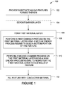
- Figure 1 depicts a method 100 for processing of substrates in accordance with some embodiments of the present invention.
- Figures 2A-F are illustrative cross-sectional views of a substrate during different stages of the method depicted in Figure 1 .
- the method 100 may be performed in any suitable substrate process chamber having both DC and radio frequency (RF) power sources, such as a process chamber 300 described below and depicted in Figure 3 .
- RF radio frequency
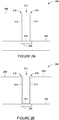
- the method 100 begins at 102, where a substrate 200 having a feature, such as opening 212, formed therein is provided, as depicted in Figure 2A .
- the substrate 200 may be any suitable substrate, such as a silicon substrate, a III-V compound substrate, a silicon germanium (SiGe) substrate, an epi-substrate, a silicon-on-insulator (SOI) substrate, a display substrate such as a liquid crystal display (LCD), a plasma display, an electro luminescence (EL) lamp display, a light emitting diode (LED) substrate, a solar cell array, solar panel, or the like.
- the substrate 200 may be a semiconductor wafer (e.g., a 200 mm, 300 mm, 450 mm, or the like silicon wafer).
- the substrate 200 may comprise one or more layers, for example, such as a bulk dielectric layer 206 formed over a dielectric layer 202, as depicted in Figure 2A .
- a conductive feature 204 may be formed in an upper region of the dielectric layer 202 such that an upper surface of the conductive feature 204 may be exposed by the opening 212 formed in the bulk dielectric layer 206.
- a via/trench etching process may be performed to define the opening 212 in the bulk dielectric layer 206, thereby exposing an upper surface of the conductive feature 204.
- the conductive feature 204 may be fabricated from any suitable conductive material.
- the conductive feature 204 may be a copper layer embedded in the dielectric layer 202.
- the conductive feature 204 may be fabricated from a metal, such as copper, aluminum, tungsten, or the like, alloys thereof, or combinations thereof.
- the bulk dielectric layer 206 and the dielectric layer 202 may be fabricated from the same or different dielectric materials.
- the dielectric materials may comprise silicon oxide (SiO 2 ), silicon nitride (SiN), a low-k material, or the like.
- the low-k material may be carbon-doped dielectric materials (such as carbon-doped silicon oxide (SiOC), BLACK DIAMOND® dielectric material available from Applied Materials, Inc. of Santa Clara, California, or the like), an organic polymer (such as polyimide, parylene, or the like), organic doped silicon glass (OSG), fluorine doped silicon glass (FSG), or the like.
- low-k materials are materials having a dielectric constant less than about that of silicon oxide, which is about 3.9.
- the opening 212 is generally defined by one or more sidewalls 214, a bottom surface 216 and upper corners (bevel) 218.
- the opening 212 may be any feature suitable for substrate fabrication, for example such as a via, a trench, a dual damascene feature, or the like, and may be formed by any suitable process or processes such as etching. Although only one opening 212 is shown, multiple features may be simultaneously processed in accordance with the teachings disclosed herein.
- the opening 212 may generally have any dimensions. For example, in some embodiments, the opening 212 may have a ratio of a height of the feature to a width of the feature of at least about 2:1. In some embodiments, the opening 212 may be a high aspect ratio feature. In such embodiments, the opening 212 may have a ratio of a height of the feature to a width of the feature of at least about 4:1. In some embodiments, the opening 212 may have a width of about 5 to about 50 nm.
- the substrate 200 is depicted as having a bulk dielectric layer 206 formed over a dielectric layer 202, the substrate 200 may also include different and/or additional material layers. In addition, other features, such as trenches, vias, or the like, may be formed in different and/or additional material layers.
- a barrier layer 208 may be optionally deposited atop the substrate 200.
- the barrier layer 208 may serve as an electrical and/or physical barrier between the substrate and layers to be subsequently deposited in the opening, and/or may function as a better surface for attachment during the deposition process discussed below than a native surface of the substrate.
- the barrier layer 208 may comprise any materials suitable to perform the above discussed functions.
- the barrier layer 208 may comprise one or more of titanium (Ti), tantalum (Ta), oxides or nitrides thereof, or the like.
- the barrier layer 208 may be deposited to any suitable thickness, for example, about 0.5 to about 10 nm.
- the barrier layer 208 may be deposited by any suitable method, for example, such as chemical vapor deposition (CVD), physical vapor deposition (PVD), or the like.
- CVD chemical vapor deposition
- PVD physical vapor deposition
- the barrier layer 208 may be deposited via a PVD process in a suitable process chamber, such as the process chamber 300 described below with respect to Figure 3 .
- the process chamber may have a target (e.g. target 342) disposed therein that comprises a source material to be deposited atop the substrate 200.
- the target may comprise tantalum (Ta).
- depositing the barrier layer 208 may include providing a process gas to the process chamber and forming a plasma from the process gas to react with source material from the target. The reaction causes the target to eject atoms of the target material, which are then directed towards the substrate 200.
- the process gas may comprise an inert gas, such as argon (Ar), helium (He), krypton (Kr), neon (Ne), xenon (Xe), or the like.
- the process gas may be provided at a flow rate of between about 2 to about 200 sccm. In some embodiments, about 5 to about 40 kW of DC power may be applied to the target to ignite the process gas and maintain a plasma.
- a bias power in the form of RF power may be applied to a substrate support pedestal (e.g., substrate support pedestal 352 discussed below) supporting the substrate 200.
- a substrate support pedestal e.g., substrate support pedestal 352 discussed below
- about 50 to about 2000 W of RF power may be supplied at a frequency of between 2 to about 60 MHz, or about 13.56 MHz.
- the process chamber may be maintained at a pressure of about 0.2 to about 50 mTorr.
- the process chamber may be maintained at a temperature of about -20 degrees Celsius to about +400 degrees Celsius.
- an initial seed layer 210 (i.e., a first material layer) may be deposited within the opening 212, as depicted in Figure 2C .
- the seed layer 210 provides a better surface for attachment and may act as a template for subsequently deposited materials, for example, such as the conductive materials discussed below.
- the seed layer 210 may comprise any materials suitable to provide the aforementioned functions.
- the seed layer may comprise one of copper (Cu), ruthenium (Ru), cobalt (Co), or the like, and alloys thereof, such as copper-aluminum (Cu-AI), copper-manganese (Cu-Mn), copper-magnesium (Cu -Mg), or the like.
- a multi-step deposition and/or etch process may be used.
- a first chamber process may be performed on the substrate 200 to form the seed layer 210.
- the initial seed layer 210 may be deposited within the opening 212 (and atop the substrate 200), as depicted in Figure 2C , using a low to medium energy process regime.
- the seed layer 210 may be deposited via any deposition process suitable to form the seed layer having a desired profile, for example, such as PVD, CVD, or the like.
- the seed layer 210 may be deposited via a PVD process in a suitable process chamber, such as the process chamber 300 described below with respect to Figure 3 .
- the process chamber may have a target (e.g. target 342) disposed therein that comprises a source material to be deposited atop the substrate 200.
- the target may comprise a copper (Cu) source material.
- depositing the seed layer 210 may include providing a process gas to the process chamber to physically sputter source material from the target, e.g., to cause the target to eject atoms of the target material, which are then directed towards the substrate 200.
- the process gas may comprise an inert gas, such as argon (Ar), helium (He), krypton (Kr), neon (Ne), xenon (Xe), or the like.
- the process gas may be provided at a flow rate of between about 4 to about 300 sccm, or in some embodiments, about 4 sccm.
- a plasma may be formed from the process gas to facilitate sputtering the source material from the target.
- a target voltage i.e., sputter voltage
- sputter voltage between -300 v to -1400 v
- an exemplary target voltage of -750v is applied to the target.
- a bias power in the form of RF power may be applied to a substrate support pedestal (e.g. , substrate support pedestal 352) supporting the substrate 200.
- a substrate support pedestal e.g. , substrate support pedestal 352 supporting the substrate 200.
- about 50 W to about 2000 W of RF power, or in some embodiments about 120 W of RF power may be supplied at a frequency of between 2 MHz to about 60 MHz, or about 13.56 MHz.
- a substrate pedestal voltage of between +150 v to -750 v may be applied.
- a substrate pedestal voltage of -120 v, to -240 v, and back to -50 v may be applied.
- the process chamber may be maintained at a pressure of about 0.1 to about 50 mTorr. In addition, in some embodiments, the process chamber may be maintained at a temperature of about 20 to about 200 degrees Celsius.
- the inventors have observed that when depositing the seed layer 210 via the low/medium energy deposition processes as described above with respect to step 108 to build the bottom substrate features 230, the seed layer material may accumulate near the upper corners 218 of the opening 212 as shown in Figure 2C . In conventional processing, the accumulation of seed layer material may partially or fully close off the opening 212 and create a void.
- a second chamber process may be performed on the substrate 200.
- the seed layer 210 is etched/resputtered in a high energy process regime to remove at least a portion of the seed layer 210 proximate the upper corners 218 of the opening 212, as depicted in Figure 2D ( e.g ., to provide an etched seed layer).
- the thickness of the seed layer 210 may be controlled at desired locations along the sidewalls 214 and proximate the upper corners 218 of the opening 212 to provide an inwardly sloped seed layer profile (e.g ., the average seed layer thickness increases from an upper portion 226, 228 of the opening 212 towards the bottom 216 of the opening 212), such as depicted in Figure 2D .
- a thickness of the seed layer 210 formed on the sidewalls 232 proximate the bottom 216 of the opening 212 may be about 2 to about 10 nm and a thickness of the seed layer 210 formed on the sidewalls 232 proximate the upper portion of the opening 212 may be about 1 to about 5 nm.
- the seed layer 210 may not be a continuous layer.
- no seed layer 210 material may be disposed on portions of the sidewalls 214 proximate the upper portion 226, 228 of the opening 212 or the upper corners 218 of the opening 212.
- the thickness of the seed layer may change dependent upon feature size.
- the seed layer thickness at the lower portion of the sidewall 232 may be more than twice of the seed layer thickness at the upper portion of the sidewall 232.
- the process gas may comprise any gas suitable to form the plasma to etch the seed layer 210, for example such as an inert gas, such as argon (Ar), helium (He), krypton (Kr), neon (Ne), xenon (Xe), or the like.
- the process gas may be provided at a flow rate of between about 10 to about 300 sccm, or in some embodiments, about 100 sccm.
- the process gas may be formed into a plasma by coupling a source power to the process gas within the process chamber under suitable conditions to establish and maintain the plasma. For example, in some embodiments, about 5 kW to about 60 kW of DC power, or in some embodiments, about 20 kW of DC power may be provided to ignite the process gas and maintain the plasma.
- a bias power may be applied to the substrate to facilitate directing ions from the plasma towards the substrate, thereby facilitating the etching process.
- the bias power applied to the substrate for the high energy process regime may between -240 V to -750 V.
- the bias power may be about 50 W to about 2000 W, or in some embodiments about 600 W at a frequency of about 2 MHz to about 60 MHz, or about 13.56 MHz.
- process chamber may be maintained at a pressure of about 1 to about 50 mTorr.
- process chamber may be maintained at a temperature of about 20 to about 200 degrees Celsius.
- a conductive material 222 may be deposited atop the seed layer 210 to fill the opening 212, as depicted in Figure 2E .
- portions of the conductive material 222 may be deposited directly atop the barrier layer 208.
- the conductive material 222 may be deposited in any manner such as electrochemical deposition, or electrochemical plating (ECP), or the like.
- the conductive material 222 may be any suitable conductive material, such as aluminum (Al), copper (Cu), or the like.
- a growth rate of the conductive material 222 during deposition may increase as the thickness of the seed layer 210 increases.
- the growth rate of the conductive material 222 may be higher when deposited atop portions of the seed layer 210 having a greater thickness (e.g . the portions of the seed layer 210 disposed on the sidewalls proximate the bottom 216 of the opening 212 and the portions of the seed layer deposited on the bottom itself) as compared to the growth rate of the conductive material 222 when deposited atop portions of the seed layer 210 having a lower thickness (e.g.
- the growth rate of the conductive material 222 may advantageously be greater proximate the bottom 216 of the opening 212, thereby allowing the opening 212 to be filled from the bottom 216 to the top. Filling the feature from the bottom 216 to the top may prevent an excess amount of conductive material 222 to form near the upper corners 218 of the feature, thereby preventing the opening 212 from being closed before fully filling the opening 212 with the conductive material 222.
- CMP chemical mechanical polishing
- the method After depositing the conductive material 222 to fill the opening 212, the method generally ends and the substrate 200 may proceed for further processing, such as deposition, etch, annealing, or the like. For example, in some embodiments additional layers may be deposited, for example additional dielectric layers and/or metallization structures may be formed over the filled opening 212.
- FIG. 3 illustrates a process chamber suitable for processing substrates in accordance with some embodiments of the present invention.
- suitable process chambers include the ENDURA® EXTENSA TTN and ENDURA® ENCORE processing chambers, both commercially available from Applied Materials, Inc., of Santa Clara, California. It is contemplated that other processing chambers, including those from other manufacturers, may also be utilized to perform the present invention.
- the processing chamber 300 contains a substrate support pedestal 352 for receiving the substrate 200 thereon, and a sputtering source, such as a target 342.
- the substrate support pedestal 352 may be located within a grounded chamber wall 350, which may be a chamber wall (as shown) or a grounded shield (not shown).
- the substrate support pedestal 352 may include any suitable means (not shown) of providing heat to the substrate 200, for example, such as a resistive heating element, radiant cavity and light source, or the like.
- the target 342 may be supported on a grounded conductive aluminum adapter 344 through a dielectric isolator 346.
- the target 342 comprises a material to be deposited on the substrate 200 during sputtering, such as titanium when depositing a titanium nitride film in accordance with embodiments of the present invention.
- the substrate support pedestal 352 has a material-receiving surface facing the principal surface of the target 342 and supports the substrate 200 to be sputter coated in planar position opposite to the principal surface of the target 342.
- the substrate support pedestal 352 may support the substrate 200 in a central region 340 of the processing chamber 300.
- the central region 340 is defined as the region above the substrate support pedestal 352 during processing (for example, between the target 342 and the substrate support pedestal 352 when in a processing position).
- the substrate support pedestal 352 is vertically movable through a bellows 358 connected to a bottom chamber wall 360 to allow the substrate 200 to be transferred onto the substrate support pedestal 352 through a load lock valve (not shown) in the lower portion of processing the chamber 300 and thereafter raised to a deposition, or processing position as depicted in Figure 3 .
- One or more processing gases may be supplied from a gas source 362 through a mass flow controller 364 into the lower part of the chamber 300.
- An exhaust port 368 may be provided and coupled to a pump (not shown) via a valve 366 for exhausting the interior of the processing chamber 300 and facilitating maintaining a desired pressure inside the processing chamber 300.
- a controllable DC power source 348 may be coupled to the chamber 300 to apply a negative voltage, or bias, to the target 342.
- An RF power supply 356 may be coupled to the substrate support pedestal 352 in order to induce a negative DC bias on the substrate 200.
- a negative DC self-bias may form on the substrate 200 during processing.
- the substrate support pedestal 352 may be grounded or left electrically floating.
- a rotatable magnetron 370 may be positioned proximate a back surface of the target 342.
- the magnetron 370 includes a plurality of magnets 372 supported by a base plate 374.
- the base plate 374 connects to a rotation shaft 376 coincident with the central axis of the chamber 300 and the substrate 200.
- the magnets 372 produce a magnetic field within the chamber 300, generally parallel and close to the surface of the target 342 to trap electrons and increase the local plasma density, which in turn increases the sputtering rate.
- the magnets 372 produce an electromagnetic field around the top of the chamber 300, and magnets 372 are rotated to rotate the electromagnetic field which influences the plasma density of the process to more uniformly sputter the target 342.
- the chamber 300 further includes a grounded bottom shield 380 connected to a ledge 384 of the adapter 344.
- a dark space shield 386 is supported on the bottom shield 380 and is fastened to the shield 380 by screws or other suitable manner.
- the metallic threaded connection between the bottom shield 380 and the dark space shield 386 allows the two shields 380, 386 to be grounded to the adapter 344.
- the adapter 344 in turn is sealed and grounded to the aluminum chamber wall 350.
- Both shields 380, 386 are typically formed from hard, non-magnetic stainless steel.
- the bottom shield 380 extends downwardly in an upper tubular portion 394 of a first diameter and a lower tubular portion 396 of a second diameter.
- the bottom shield 380 extends along the walls of the adapter 344 and the chamber wall 350 downwardly to below a top surface of the substrate support pedestal 352 and returns upwardly until reaching a top surface of the substrate support pedestal 352 (e.g., forming a u-shaped portion 398 at the bottom).
- a cover ring 302 rests on the top of the upwardly extending inner portion of the bottom shield 380 when the substrate support pedestal 352 is in its lower, loading position but rests on the outer periphery of the substrate support pedestal 352 when it is in its upper, deposition position to protect the substrate support pedestal 352 from sputter deposition.
- An additional deposition ring (not shown) may be used to shield the periphery of the substrate 200 from deposition.
- An RF coil 304 may be disposed just outside the periphery of the substrate 200 in a lower half or third of the space between the target 342 and the substrate support pedestal 352.
- Multiple insulating supports (not shown) in the bottom shield 380 support the RF coil 304 and also supply RF power and grounding to the RF coil 304.
- the coil 304 may be a single-turn, nearly tubular coil composed of copper and having a small gap between the closely spaced electrical leads for power and grounding.
- An RF power supply 308 may be provided to supply RF power to the RF coil 304 to generate an argon plasma in a region removed from the target 342.
- the target 342 may be DC powered for sputter deposition and the RF coil 304 may be utilized for sputter etching of the substrate 200. However, in some embodiments , any combination of DC and RF power may power the two step DCE processes.
- the chamber 300 may also be adapted to provide a more directional sputtering of material onto a substrate.
- directional sputtering may be achieved by positioning an optional collimator 310 between the target 342 and the substrate support pedestal 352 to provide a more uniform and symmetrical flux of deposition material to the substrate 200.
- the collimator 310 when present, may rest on the ledge portion of the bottom shield 380, thereby grounding the collimator 310.
- the collimator 310 may be a metal ring and may include an outer tubular section and at least one inner concentric tubular section, for example, three concentric tubular sections 312, 314, 316 linked by cross struts 320, 318.
- the outer tubular section 316 rests on the ledge portion 306 of the bottom shield 380.
- the use of the bottom shield 380 to support the collimator 310 simplifies the design and maintenance of the chamber 300.
- At least the two inner tubular sections 312, 314 are of sufficient height to define high aspect ratio apertures that partially collimate the sputtered particles.
- the upper surface of the collimator 310 acts as a ground plane in opposition to the biased target 342, which facilitates keeping plasma electrons away from the substrate 200.
- a magnet 354 may be disposed about the chamber 300 for selectively providing a magnetic field between the substrate support pedestal 352 and the target 342.
- the magnet 354 may be disposed about the outside of the chamber wall 350 in a region just above the substrate support pedestal 352 when in processing position.
- the magnet 354 may be an electromagnet and may be coupled to a power source (not shown) for controlling the magnitude of the magnetic field generated by the electromagnet.
- a process controller 330 is coupled to various components of the process chamber 300 for controlling the operation thereof and comprises a central processing unit (CPU) 332, a memory 334, and support circuits 336 for the CPU 332.
- the process controller 330 may control the substrate processing apparatus directly, or via computers (or controllers) associated with particular process chamber and/or the support system components.
- the process controller 330 may be one of any form of general-purpose computer processor that can be used in an industrial setting for controlling various chambers and sub-processors.
- the memory, or computer-readable medium, 334 of the CPU 332 may be one or more of readily available memory such as random access memory (RAM), read only memory (ROM), floppy disk, hard disk, flash, or any other form of digital storage, local or remote.
- the support circuits 336 are coupled to the CPU 332 for supporting the processor in a conventional manner. These circuits include cache, power supplies, clock circuits, input/output circuitry and subsystems, and the like. Inventive methods as described herein may be stored in the memory 334 as software routine that may be executed or invoked to control the operation of the process chamber 300 in the manner described herein. The software routine may also be stored and/or executed by a second CPU (not shown) that is remotely located from the hardware being controlled by the CPU 332.
- a synchronization controller 322 (described below in more detail with respect to Figure 5 ) is coupled to various components of the process chamber 300 for controlling the operation thereof and comprises a central processing unit (CPU) 324, a memory 326, and support circuits 328 for the CPU 324.
- the synchronization controller 322 may receive process parameters for a sub-set of substrate processing support systems from the process controller 330.
- the synchronization controller 322 may receive process parameters for RF power supplies 308 and 356, DC power source 348, and optionally magnetron 370 from the process controller 330.
- the synchronization controller 322 may control these systems directly, or via computers (or controllers) associated the support system components.
- the synchronization controller 322 may be one of any form of general-purpose computer processor that can be used in an industrial setting for controlling various support systems and sub-processors.
- the memory, or computer-readable medium, 326 of the CPU 324 may be one or more of readily available memory such as random access memory (RAM), read only memory (ROM), floppy disk, hard disk, flash, or any other form of digital storage, local or remote.
- the support circuits 328 are coupled to the CPU 324 for supporting the processor in a conventional manner. These circuits include cache, power supplies, clock circuits, input/output circuitry and subsystems, and the like.
- Inventive methods as described herein may be stored in the memory 326 as software routine that may be executed or invoked to control the operation of selected support devices (e.g., power supplies) associated with process chamber 300 in the manner described herein, for example, such as described above with respect to the methods 100 and 600.
- the software routine may also be stored and/or executed by a second CPU (not shown) that is remotely located from the hardware being controlled by the CPU 324.
- a substrate processing tool may have numerous process chambers and network nodes for communication with devices and power supplies.
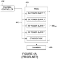
- a central "real time" process controller 402 is used to coordinate the signals to all the devices 406 a-n over a shared network connection 410 as shown in Figure 4A .
- a process controller 402 may send all process parameters for devices 406 a-n required to perform a specific deposition process in chamber 408, for example, to the devices 406 a-n in device rack 404 over a shared network 410.
- devices may be delayed in receiving their operating instructions for performing the specific deposition process.
- each device e.g., internal signal processing and power cycling time of a power supply.
- the sum of these delays has been shown to be above 300 ms in some cases.
- signaling delays show the actual power applied and removed at different times. These delays also vary depending on how many systems may be attached to the process controller.
- the individual process recipes described above can be between 2 to 5 seconds in duration. With delay times, the actual results can vary significantly, as demonstrated by film thickness variations across the wafer and from wafer-to-wafer since the timing is not precise.
- the inventors have observed that by synchronizing the sending of process parameters (e.g ., magnetron position, electromagnet current, DC and RF powers, temperature, pressure, etc.), using direct communication lines to each of the devices, and taking into account the intrinsic delays associated with each device, improvements can be realized in deposition performance (step coverage, uniformity), repeatability of process results, and reliability of hardware components.
- process parameters e.g ., magnetron position, electromagnet current, DC and RF powers, temperature, pressure, etc.
- improvements can be realized in deposition performance (step coverage, uniformity), repeatability of process results, and reliability of hardware components.
- a separate programmable synchronization controller 504 as shown in control system 500 of Figure 5 , to synchronize the sending of process parameters, delay times for controlling power supplies, for example, can be greatly decreased.
- the synchronization controller 504 described here may be used as the synchronization controller 322 described above with respect to Figure 3 .
- Figure 6 depicts and exemplary method 600 that may be performed by the synchronization controller 504 in Figure 5 and synchronization controller 322 described above with respect to Figure 3 .
- the method 600 begins at 602 where the synchronization controller 504 receives process control parameters for one or more devices 506 1-n from a process controller 502 over link 510 to perform, for example, a first deposition chamber process in chamber 508.
- the synchronization controller 504 determines a time to send each of the process control parameters to the one or more devices 506 1-n using information contained in the process control parameters.
- the synchronization controller 504 will adjust the determined time to send each of the process control parameters using specific signal process delays (e.g., intrinsic delays) associated with each of the one or more devices 506 1-n .
- the synchronization controller will send the process control parameters to each of the one or more devices 506 1-n at the adjusted times to perform the first chamber process.
- each device of the one or more devices 506 1-n is controlled by the synchronization controller 504 using process control parameters sent on the output channel directly coupled to an analog control port of the device in step 610.
- the process control parameters are received in a digital format from the process controller, and the synchronization controller 504 converts the digital process control parameters for each device into analog signals to be sent to and control each of the one or more devices 506 1-n .
- the act of sending the process control parameters to the one or more devices at the adjusted time includes sending the analog signals corresponding to the process control parameters separately to each of the one or more devices over each channel directly coupled to one of the one or more devices.
- the synchronization controller 504 will wait until all process control parameters are received and will synchronize the sending of the process control parameters to each of the one or more devices 506 1-n .
- Synchronizing the sending of process control parameters to each of the one or more devices 506 1-n may include sending control signals to each of the one or more devices 506 1-n simultaneously (in parallel) over one or more output channels 512 1-n , where each channel is directly coupled to one of the one or more devices channel directly coupled to analog control ports on each of the one or more devices 506 1-n .
- output channels 512 1-n may be coupled to more than one device that are not used simultaneously in the same substrate process chamber process.
- the length of signal conductors to each of the one or more devices 506 1-n do not need to be the same length.
- each of the one or more devices may be controlled by the synchronization controller 504 at step 606 using process control parameters sent on the output channel 512 1-n directly coupled to the control port of the device.
- Each of the one or more devices 506 1-n may then supply the specified power, or substrate support process, as appropriate, to chamber 508.
- the first deposition process may be a first DCE process where metal (e.g. , Cu) ions are to be deposited on a substrate using a low energy process regime to build the bottom of a feature on the substrate.
- the synchronization controller 504 will receive all the necessary process parameters for the one or more devices 506 1-n used in first chamber process from process controller 502.
- the synchronization controller 504 will simultaneously (in parallel) send the necessary process parameters directly to controls ports on DC power supplies 506 1 and 506 2 over output channels 512 1 and 512 2 to shut off, and to controls ports on RF power supplies 506 3 and 506 4 over output channels 512 3 and 512 4 to turn on.
- the inventors have discovered that in embodiments of the present invention discussed above, synchronization of DC and RF power supply response times have been improved from 300ms delay to 30ms delay. As such, each device will essentially receive the required processing parameters substantially at the same time (i.e., with minimal delays) and will more closely match an ideal setpoint for required power.
- the process parameters received by synchronization controller 504 may be in the form of packet data for controlling each device 506 1-n .
- Each device 506 1-n may require a different data/signaling format for interfacing with the device. Conversions of the process parameters to control each device 506 1-n may be performed by process controller 502 or by synchronization controller 504.
- processes other than deposition processes may be performed by the control system 500.
- synchronization controller 504 may be used to control pressure systems, temperature systems, magnetron assemblies, or any other devices that may be controlled for use in substrate processing.
Description
- Embodiments of the present invention generally relate to controlling processing conditions during physical vapor deposition processes
- Integrated circuits have evolved into complex devices that can include millions of components (e.g., transistors, capacitors and resistors) on a single chip. The evolution of chip designs continually requires faster circuitry and greater circuit density. The demands for greater circuit density necessitate a reduction in the dimensions of the integrated circuit components. As the dimensions decrease, processing of the integrated chip substrates become increasingly more challenging.
- For example, in conventional substrate processing, thin layers of material are applied to the inner surfaces of substrate features prior to filling the feature with conductive material. Ideally, the thin layer would be consistent throughout the feature, while minimizing overhang (excessive material on surfaces of the opening of the feature), which can reduce the size of the feature opening, or close the opening completely (undesirably leaving an air gap, or void, trapped within the feature). As the dimensions of the integrated circuit components decrease, the aspect ratio of the height of the feature to the width of the feature increases, further exacerbating the challenge of consistent deposition of the thin layer.
- Typical processes commonly used for fabricating integrated circuits having such high aspect ratio features include depositing material in a bottom of the features and re-sputtering the material to facilitate redistribution from the bottom to the sidewalls of the feature. This is done using high energy ions directed toward the substrate. Unfortunately, this method may cause damage to the underlying layers and the substrate itself, particularly at the corners, or bevel, and bottom of the feature. This damage results in significant line resistance increase and reliability degradation. In addition, unfavorable results of typical processes include overhang buildup, which may close up the feature, with the effect becoming more prevalent at smaller feature geometries (e.g., at higher aspect ratios).
- Furthermore, the inventors have observed that attempts to solve the aforementioned problems by varying the ion density and energy through controlling the DC, RF powers and electromagnet current results film thickness variations across the wafer and from wafer-to-wafer due to delays in signal processing with respect to the power supplies.
JP2011149093 - Therefore, the inventors have provided improved methods for forming thin layers of material to the inner surfaces of high aspect ratio features.
- Methods and apparatus for processing a substrate are provided herein. In some embodiments, a method for processing a substrate in a process chamber, includes receiving, by the synchronization controller, process control parameters for one or more devices from a process controller to perform a first chamber process, determining, by the synchronization controller, a time to send each of the process control parameters to the one or more devices, for each of the one or more devices, adjusting, by the synchronization controller, the determined time to send each of the process control parameters using specific signal process delays associated with each of the one or more devices wherein the specific signal processing delays include intrinsic delays associated with each of the one or more devices, and sending, by the synchronization controller, the process control parameters to each of the one or more devices at the adjusted times to perform the first chamber process, wherein the synchronization controller includes one or more output channels, each channel directly coupled to one of the one or more devices.
- In some embodiments, a substrate processing system includes a synchronization controller having one or more inputs to receive process control parameters of one or more devices from a process controller, and one or more output channels, each output channel directly coupled to one of the one or more devices, wherein the synchronization controller is configured to (a) receive the process control parameters, (b) determine a time to send each of the process control parameters to the one or more devices, c) for each of the one or more devices, adjust the determined time to send each of the process control parameters using specific signal process delays associated with each of the one or more devices, wherein the specific signal processing delays include intrinsic delays associated with each of the one or more devices, and (d) send the process control parameters to each of the one or more devices at the adjusted times to perform a first chamber process.
- In an example useful for understanding the invention, a method for forming layers on a substrate having one or more features includes performing a first substrate process on the first layer using a first energy process regime to build up a bottom portion of the one or more features with the first material and performing a second substrate process on the first layer using a second energy process regime to redistribute the first material from the bottom portion of the one or more features to a sidewall of the one or more features, wherein the second energy process regime is higher than the first energy process regime.
- Embodiments of the present invention, briefly summarized above and discussed in greater detail below, can be understood by reference to the illustrative embodiments of the invention depicted in the appended drawings. It is to be noted, however, that the appended drawings illustrate only typical embodiments of this invention and are therefore not to be considered limiting of its scope, for the invention may admit to other equally effective embodiments.
-
Figure 1 depicts a method for the processing of a semiconductor substrate in accordance with some embodiments of the present invention. -
Figures 2A-2F are illustrative cross-sectional views of a substrate during different stages of the processing sequence in accordance with some embodiments of the present invention. -
Figure 3 depicts an apparatus suitable for processing semiconductor substrates in accordance with some embodiments of the present invention. -
Figure 4A is a schematic of a conventional control system for controlling support systems in substrate processing. -
Figure 4B is a chart showing an exemplary signal delay associated with conventional control systems for controlling support systems in substrate processing. -
Figure 5 is a schematic of an exemplary control system including a separate synchronization controller in accordance with some embodiments of the present invention. -
Figure 6 depicts a method for synchronizing the control of support systems associated with processing of a semiconductor substrate in accordance with some embodiments of the present invention. - To facilitate understanding, identical reference numerals have been used, where possible, to designate identical elements that are common to the figures. The figures are not drawn to scale and may be simplified for clarity. It is contemplated that elements and features of one embodiment may be beneficially incorporated in other embodiments without further recitation.
- In ionized physical vapor deposition (PVD) copper processes, metal ions are accelerated from a target source material and deposited into via and trench structures (i.e., features) formed on a substrate. The inventors have discovered that by varying the ion density and energy, step coverage of the feature (e.g., a thickness of the deposited material on horizontal surfaces as compared to a thickness of the deposited material on vertical surfaces) may be tailored by adjusting the ion/neutral metal ratio, trajectory and sputter yield. Typically a PVD copper deposition process is operated in the high metal ion ratio regime at varying ion energies. By varying the energy of incoming ions, distinct process regimes are realized. At medium ion energy process regimes, a high bottom deposition process is observed with minimum resputtering on the substrate. At higher energy process regimes, the ions may physically etch the substrate. The inventors have discovered that combining the medium energy and high energy processes, in a multi-step process, favorable step coverage for copper ion reflow or electrochemical deposition, or plating (ECP) gap fill may be realized while minimizing or preventing damage to the substrate or the feature.
- In addition, the inventors have also observed that by synchronizing the sending of process parameters (e.g., magnetron position, electromagnet current, DC and RF powers), improvements can be realized in deposition performance (step coverage, uniformity), repeatability of process results, and reliability of hardware components. By using a separate programmable logic controller to synchronize the sending of process parameters, delay times for controlling power supplies, for example, can be greatly decreased. Specifically, in embodiments, synchronization of DC and RF power supply response times have been improved from, for example, 300ms delay to 30ms delay. The inventors have also observed that by synchronizing the DC and RF power supply response times, substrate wafer edge uniformity has been improved, for example, from 7% to 2.5%. In addition, in at least some embodiments, wafer-to-wafer repeatability is also improved by a similar margin. Furthermore, by synchronizing the sending of process parameters to the process devices, arcing within the process chamber may be prevented by more accurately controlling when certain devices are turned on and off.
-
Figure 1 depicts amethod 100 for processing of substrates in accordance with some embodiments of the present invention.Figures 2A-F are illustrative cross-sectional views of a substrate during different stages of the method depicted inFigure 1 . Themethod 100 may be performed in any suitable substrate process chamber having both DC and radio frequency (RF) power sources, such as aprocess chamber 300 described below and depicted inFigure 3 . - The
method 100 begins at 102, where asubstrate 200 having a feature, such as opening 212, formed therein is provided, as depicted inFigure 2A . Thesubstrate 200 may be any suitable substrate, such as a silicon substrate, a III-V compound substrate, a silicon germanium (SiGe) substrate, an epi-substrate, a silicon-on-insulator (SOI) substrate, a display substrate such as a liquid crystal display (LCD), a plasma display, an electro luminescence (EL) lamp display, a light emitting diode (LED) substrate, a solar cell array, solar panel, or the like. In some embodiments, thesubstrate 200 may be a semiconductor wafer (e.g., a 200 mm, 300 mm, 450 mm, or the like silicon wafer). - In some embodiments, the
substrate 200 may comprise one or more layers, for example, such as a bulkdielectric layer 206 formed over adielectric layer 202, as depicted inFigure 2A . Aconductive feature 204 may be formed in an upper region of thedielectric layer 202 such that an upper surface of theconductive feature 204 may be exposed by theopening 212 formed in the bulkdielectric layer 206. For example, a via/trench etching process may be performed to define theopening 212 in the bulkdielectric layer 206, thereby exposing an upper surface of theconductive feature 204. Theconductive feature 204 may be fabricated from any suitable conductive material. For example, for a copper interconnect, theconductive feature 204 may be a copper layer embedded in thedielectric layer 202. In some embodiments, theconductive feature 204 may be fabricated from a metal, such as copper, aluminum, tungsten, or the like, alloys thereof, or combinations thereof. - The bulk
dielectric layer 206 and thedielectric layer 202 may be fabricated from the same or different dielectric materials. In some embodiments, the dielectric materials may comprise silicon oxide (SiO2), silicon nitride (SiN), a low-k material, or the like. The low-k material may be carbon-doped dielectric materials (such as carbon-doped silicon oxide (SiOC), BLACK DIAMOND® dielectric material available from Applied Materials, Inc. of Santa Clara, California, or the like), an organic polymer (such as polyimide, parylene, or the like), organic doped silicon glass (OSG), fluorine doped silicon glass (FSG), or the like. As used herein, low-k materials are materials having a dielectric constant less than about that of silicon oxide, which is about 3.9. - The
opening 212 is generally defined by one or more sidewalls 214, abottom surface 216 and upper corners (bevel) 218. Theopening 212 may be any feature suitable for substrate fabrication, for example such as a via, a trench, a dual damascene feature, or the like, and may be formed by any suitable process or processes such as etching. Although only oneopening 212 is shown, multiple features may be simultaneously processed in accordance with the teachings disclosed herein. Theopening 212 may generally have any dimensions. For example, in some embodiments, theopening 212 may have a ratio of a height of the feature to a width of the feature of at least about 2:1. In some embodiments, theopening 212 may be a high aspect ratio feature. In such embodiments, theopening 212 may have a ratio of a height of the feature to a width of the feature of at least about 4:1. In some embodiments, theopening 212 may have a width of about 5 to about 50 nm. - Although the
substrate 200 is depicted as having abulk dielectric layer 206 formed over adielectric layer 202, thesubstrate 200 may also include different and/or additional material layers. In addition, other features, such as trenches, vias, or the like, may be formed in different and/or additional material layers. - Next, at 104, a
barrier layer 208 may be optionally deposited atop thesubstrate 200. When present, thebarrier layer 208 may serve as an electrical and/or physical barrier between the substrate and layers to be subsequently deposited in the opening, and/or may function as a better surface for attachment during the deposition process discussed below than a native surface of the substrate. Thebarrier layer 208 may comprise any materials suitable to perform the above discussed functions. For example, in some embodiments, thebarrier layer 208 may comprise one or more of titanium (Ti), tantalum (Ta), oxides or nitrides thereof, or the like. Thebarrier layer 208 may be deposited to any suitable thickness, for example, about 0.5 to about 10 nm. - The
barrier layer 208 may be deposited by any suitable method, for example, such as chemical vapor deposition (CVD), physical vapor deposition (PVD), or the like. For example, in some embodiments, thebarrier layer 208 may be deposited via a PVD process in a suitable process chamber, such as theprocess chamber 300 described below with respect toFigure 3 . In such embodiments, the process chamber may have a target (e.g. target 342) disposed therein that comprises a source material to be deposited atop thesubstrate 200. For example, in embodiments where the barrier layer comprises tantalum nitride (TaNx), the target may comprise tantalum (Ta). - In some embodiments, depositing the
barrier layer 208 may include providing a process gas to the process chamber and forming a plasma from the process gas to react with source material from the target. The reaction causes the target to eject atoms of the target material, which are then directed towards thesubstrate 200. In some embodiments, the process gas may comprise an inert gas, such as argon (Ar), helium (He), krypton (Kr), neon (Ne), xenon (Xe), or the like. The process gas may be provided at a flow rate of between about 2 to about 200 sccm. In some embodiments, about 5 to about 40 kW of DC power may be applied to the target to ignite the process gas and maintain a plasma. - In some embodiments, to facilitate directing the ejected atoms from the target towards the substrate 200 a bias power in the form of RF power may be applied to a substrate support pedestal (e.g.,
substrate support pedestal 352 discussed below) supporting thesubstrate 200. In such embodiments about 50 to about 2000 W of RF power may be supplied at a frequency of between 2 to about 60 MHz, or about 13.56 MHz. - In addition to the above, additional process parameters may be utilized to facilitate depositing the
barrier layer 208. For example, in some embodiments, the process chamber may be maintained at a pressure of about 0.2 to about 50 mTorr. In addition, in some embodiments, the process chamber may be maintained at a temperature of about -20 degrees Celsius to about +400 degrees Celsius. - Next, at 106, an initial seed layer 210 (i.e., a first material layer) may be deposited within the
opening 212, as depicted inFigure 2C . Theseed layer 210 provides a better surface for attachment and may act as a template for subsequently deposited materials, for example, such as the conductive materials discussed below. Theseed layer 210 may comprise any materials suitable to provide the aforementioned functions. For example, in some embodiments, the seed layer may comprise one of copper (Cu), ruthenium (Ru), cobalt (Co), or the like, and alloys thereof, such as copper-aluminum (Cu-AI), copper-manganese (Cu-Mn), copper-magnesium (Cu -Mg), or the like. - To form the initial seed layer 210 (e.g., a first material layer), in some embodiments, a multi-step deposition and/or etch process may be used. First at 108, a first chamber process may be performed on the
substrate 200 to form theseed layer 210. In some embodiments, theinitial seed layer 210 may be deposited within the opening 212 (and atop the substrate 200), as depicted inFigure 2C , using a low to medium energy process regime. Theseed layer 210 may be deposited via any deposition process suitable to form the seed layer having a desired profile, for example, such as PVD, CVD, or the like. For example, in some embodiments, theseed layer 210 may be deposited via a PVD process in a suitable process chamber, such as theprocess chamber 300 described below with respect toFigure 3 . In such embodiments, the process chamber may have a target (e.g. target 342) disposed therein that comprises a source material to be deposited atop thesubstrate 200. For example, in embodiments where theseed layer 210 comprises copper (Cu), the target may comprise a copper (Cu) source material. - In some embodiments, depositing the
seed layer 210 may include providing a process gas to the process chamber to physically sputter source material from the target, e.g., to cause the target to eject atoms of the target material, which are then directed towards thesubstrate 200. In some embodiments, the process gas may comprise an inert gas, such as argon (Ar), helium (He), krypton (Kr), neon (Ne), xenon (Xe), or the like. The process gas may be provided at a flow rate of between about 4 to about 300 sccm, or in some embodiments, about 4 sccm. In some embodiments, a plasma may be formed from the process gas to facilitate sputtering the source material from the target. In such embodiments, about 5 kW to about 60 kW of DC power, or in some embodiments, about 30 kW of DC power may be applied to the target to ignite the process gas and maintain the plasma. A target voltage (i.e., sputter voltage) between -300 v to -1400 v may be applied to the target to induce sputtering. In some embodiments, an exemplary target voltage of -750v is applied to the target. By using a low/medium DC energy process regime to sputter the target material in combination with applying RF bias energy, the target source material ions (e.g., Cu ions) enter the feature of the substrate (e.g., via and/or trench) at a nearly vertical trajectory. Due to the low energy of the target source material ions, a bottom portion of thefeature 230 is built up with target source material ions that don't resputter to other portions of the substrate. - In some embodiments, to facilitate directing the ejected atoms from the target towards the substrate 200 a bias power in the form of RF power may be applied to a substrate support pedestal (e.g., substrate support pedestal 352) supporting the
substrate 200. In such embodiments, about 50 W to about 2000 W of RF power, or in some embodiments about 120 W of RF power may be supplied at a frequency of between 2 MHz to about 60 MHz, or about 13.56 MHz. In addition, in some embodiments a substrate pedestal voltage of between +150 v to -750 v may be applied. In an exemplary multistep deposition/etch process, a substrate pedestal voltage of -120 v, to -240 v, and back to -50 v may be applied. - In addition to the above, additional process parameters may be utilized to facilitate depositing the
seed layer 210. For example, in some embodiments, the process chamber may be maintained at a pressure of about 0.1 to about 50 mTorr. In addition, in some embodiments, the process chamber may be maintained at a temperature of about 20 to about 200 degrees Celsius. - In some embodiments, the inventors have observed that when depositing the
seed layer 210 via the low/medium energy deposition processes as described above with respect to step 108 to build the bottom substrate features 230, the seed layer material may accumulate near theupper corners 218 of theopening 212 as shown inFigure 2C . In conventional processing, the accumulation of seed layer material may partially or fully close off theopening 212 and create a void. - Accordingly, at 110 a second chamber process may be performed on the
substrate 200. At 110, theseed layer 210 is etched/resputtered in a high energy process regime to remove at least a portion of theseed layer 210 proximate theupper corners 218 of theopening 212, as depicted inFigure 2D (e.g., to provide an etched seed layer). By etching/resputtering at least a portion of theseed layer 210, the thickness of theseed layer 210 may be controlled at desired locations along thesidewalls 214 and proximate theupper corners 218 of theopening 212 to provide an inwardly sloped seed layer profile (e.g., the average seed layer thickness increases from anupper portion opening 212 towards thebottom 216 of the opening 212), such as depicted inFigure 2D . For example, in some embodiments, a thickness of theseed layer 210 formed on thesidewalls 232 proximate the bottom 216 of theopening 212 may be about 2 to about 10 nm and a thickness of theseed layer 210 formed on thesidewalls 232 proximate the upper portion of theopening 212 may be about 1 to about 5 nm. In some embodiments, theseed layer 210 may not be a continuous layer. For example, in some embodiments, noseed layer 210 material may be disposed on portions of thesidewalls 214 proximate theupper portion opening 212 or theupper corners 218 of theopening 212. The thickness of the seed layer may change dependent upon feature size. In some embodiments, the seed layer thickness at the lower portion of thesidewall 232 may be more than twice of the seed layer thickness at the upper portion of thesidewall 232. - The process gas may comprise any gas suitable to form the plasma to etch the
seed layer 210, for example such as an inert gas, such as argon (Ar), helium (He), krypton (Kr), neon (Ne), xenon (Xe), or the like. The process gas may be provided at a flow rate of between about 10 to about 300 sccm, or in some embodiments, about 100 sccm. The process gas may be formed into a plasma by coupling a source power to the process gas within the process chamber under suitable conditions to establish and maintain the plasma. For example, in some embodiments, about 5 kW to about 60 kW of DC power, or in some embodiments, about 20 kW of DC power may be provided to ignite the process gas and maintain the plasma. In some embodiments, a bias power may be applied to the substrate to facilitate directing ions from the plasma towards the substrate, thereby facilitating the etching process. In some embodiments, the bias power applied to the substrate for the high energy process regime may between -240 V to -750 V. For example, in some embodiments, the bias power may be about 50 W to about 2000 W, or in some embodiments about 600 W at a frequency of about 2 MHz to about 60 MHz, or about 13.56 MHz. - In addition to the above, additional process parameters may be utilized to facilitate etching/resputtering the
seed layer 210. For example, in some embodiments, the process chamber may be maintained at a pressure of about 1 to about 50 mTorr. In addition, in some embodiments, the process chamber may be maintained at a temperature of about 20 to about 200 degrees Celsius. - Next, at 112, a
conductive material 222 may be deposited atop theseed layer 210 to fill theopening 212, as depicted inFigure 2E . In embodiments where theseed layer 210 does not form a continuous layer (described above), portions of theconductive material 222 may be deposited directly atop thebarrier layer 208. Theconductive material 222 may be deposited in any manner such as electrochemical deposition, or electrochemical plating (ECP), or the like. Theconductive material 222 may be any suitable conductive material, such as aluminum (Al), copper (Cu), or the like. - In some embodiments, the inventors have observed that a growth rate of the
conductive material 222 during deposition may increase as the thickness of theseed layer 210 increases. For example, in some embodiments, the growth rate of theconductive material 222 may be higher when deposited atop portions of theseed layer 210 having a greater thickness (e.g. the portions of theseed layer 210 disposed on the sidewalls proximate the bottom 216 of theopening 212 and the portions of the seed layer deposited on the bottom itself) as compared to the growth rate of theconductive material 222 when deposited atop portions of theseed layer 210 having a lower thickness (e.g. the portions of theseed layer 210 disposed on the sidewalls proximate the top of theopening 212 and the portions of the seed layer deposited on the upper corners 218). Accordingly, by providing theseed layer 210 having a sloped profile (as discussed above) the growth rate of theconductive material 222 may advantageously be greater proximate the bottom 216 of theopening 212, thereby allowing theopening 212 to be filled from the bottom 216 to the top. Filling the feature from the bottom 216 to the top may prevent an excess amount ofconductive material 222 to form near theupper corners 218 of the feature, thereby preventing theopening 212 from being closed before fully filling theopening 212 with theconductive material 222. - After filling the
opening 212 with theconductive material 222, chemical mechanical polishing (CMP) or other suitable technique may be used to remove the excessconductive material 222 outside the opening 212 (and any other features, such as other vias, trenches, dual damascene structures, or the like), as depicted inFigure 2F . - After depositing the
conductive material 222 to fill theopening 212, the method generally ends and thesubstrate 200 may proceed for further processing, such as deposition, etch, annealing, or the like. For example, in some embodiments additional layers may be deposited, for example additional dielectric layers and/or metallization structures may be formed over the filledopening 212. - The inventive methods described herein may be performed in a process chamber as described below.
Figure 3 illustrates a process chamber suitable for processing substrates in accordance with some embodiments of the present invention. Examples of suitable process chambers include the ENDURA® EXTENSA TTN and ENDURA® ENCORE processing chambers, both commercially available from Applied Materials, Inc., of Santa Clara, California. It is contemplated that other processing chambers, including those from other manufacturers, may also be utilized to perform the present invention. - In some embodiments, the
processing chamber 300 contains asubstrate support pedestal 352 for receiving thesubstrate 200 thereon, and a sputtering source, such as atarget 342. Thesubstrate support pedestal 352 may be located within a groundedchamber wall 350, which may be a chamber wall (as shown) or a grounded shield (not shown). Thesubstrate support pedestal 352 may include any suitable means (not shown) of providing heat to thesubstrate 200, for example, such as a resistive heating element, radiant cavity and light source, or the like. - The
target 342 may be supported on a groundedconductive aluminum adapter 344 through adielectric isolator 346. Thetarget 342 comprises a material to be deposited on thesubstrate 200 during sputtering, such as titanium when depositing a titanium nitride film in accordance with embodiments of the present invention. - The
substrate support pedestal 352 has a material-receiving surface facing the principal surface of thetarget 342 and supports thesubstrate 200 to be sputter coated in planar position opposite to the principal surface of thetarget 342. Thesubstrate support pedestal 352 may support thesubstrate 200 in acentral region 340 of theprocessing chamber 300. Thecentral region 340 is defined as the region above thesubstrate support pedestal 352 during processing (for example, between thetarget 342 and thesubstrate support pedestal 352 when in a processing position). - The
substrate support pedestal 352 is vertically movable through abellows 358 connected to abottom chamber wall 360 to allow thesubstrate 200 to be transferred onto thesubstrate support pedestal 352 through a load lock valve (not shown) in the lower portion of processing thechamber 300 and thereafter raised to a deposition, or processing position as depicted inFigure 3 . One or more processing gases may be supplied from agas source 362 through amass flow controller 364 into the lower part of thechamber 300. Anexhaust port 368 may be provided and coupled to a pump (not shown) via avalve 366 for exhausting the interior of theprocessing chamber 300 and facilitating maintaining a desired pressure inside theprocessing chamber 300. - A controllable
DC power source 348 may be coupled to thechamber 300 to apply a negative voltage, or bias, to thetarget 342. AnRF power supply 356 may be coupled to thesubstrate support pedestal 352 in order to induce a negative DC bias on thesubstrate 200. In addition, in some embodiments, a negative DC self-bias may form on thesubstrate 200 during processing. In other applications, thesubstrate support pedestal 352 may be grounded or left electrically floating. - A
rotatable magnetron 370 may be positioned proximate a back surface of thetarget 342. Themagnetron 370 includes a plurality ofmagnets 372 supported by abase plate 374. Thebase plate 374 connects to arotation shaft 376 coincident with the central axis of thechamber 300 and thesubstrate 200. Themagnets 372 produce a magnetic field within thechamber 300, generally parallel and close to the surface of thetarget 342 to trap electrons and increase the local plasma density, which in turn increases the sputtering rate. Themagnets 372 produce an electromagnetic field around the top of thechamber 300, andmagnets 372 are rotated to rotate the electromagnetic field which influences the plasma density of the process to more uniformly sputter thetarget 342. - The
chamber 300 further includes a groundedbottom shield 380 connected to aledge 384 of theadapter 344. Adark space shield 386 is supported on thebottom shield 380 and is fastened to theshield 380 by screws or other suitable manner. The metallic threaded connection between thebottom shield 380 and thedark space shield 386 allows the twoshields adapter 344. Theadapter 344 in turn is sealed and grounded to thealuminum chamber wall 350. Both shields 380, 386 are typically formed from hard, non-magnetic stainless steel. - The
bottom shield 380 extends downwardly in an uppertubular portion 394 of a first diameter and a lowertubular portion 396 of a second diameter. Thebottom shield 380 extends along the walls of theadapter 344 and thechamber wall 350 downwardly to below a top surface of thesubstrate support pedestal 352 and returns upwardly until reaching a top surface of the substrate support pedestal 352 (e.g., forming au-shaped portion 398 at the bottom). Acover ring 302 rests on the top of the upwardly extending inner portion of thebottom shield 380 when thesubstrate support pedestal 352 is in its lower, loading position but rests on the outer periphery of thesubstrate support pedestal 352 when it is in its upper, deposition position to protect thesubstrate support pedestal 352 from sputter deposition. An additional deposition ring (not shown) may be used to shield the periphery of thesubstrate 200 from deposition. - An
RF coil 304 may be disposed just outside the periphery of thesubstrate 200 in a lower half or third of the space between thetarget 342 and thesubstrate support pedestal 352. Multiple insulating supports (not shown) in thebottom shield 380 support theRF coil 304 and also supply RF power and grounding to theRF coil 304. Thecoil 304 may be a single-turn, nearly tubular coil composed of copper and having a small gap between the closely spaced electrical leads for power and grounding. AnRF power supply 308 may be provided to supply RF power to theRF coil 304 to generate an argon plasma in a region removed from thetarget 342. Thetarget 342 may be DC powered for sputter deposition and theRF coil 304 may be utilized for sputter etching of thesubstrate 200. However, in some embodiments , any combination of DC and RF power may power the two step DCE processes. - The
chamber 300 may also be adapted to provide a more directional sputtering of material onto a substrate. In some embodiments, directional sputtering may be achieved by positioning anoptional collimator 310 between thetarget 342 and thesubstrate support pedestal 352 to provide a more uniform and symmetrical flux of deposition material to thesubstrate 200. - The
collimator 310, when present, may rest on the ledge portion of thebottom shield 380, thereby grounding thecollimator 310. Thecollimator 310 may be a metal ring and may include an outer tubular section and at least one inner concentric tubular section, for example, three concentrictubular sections tubular section 316 rests on theledge portion 306 of thebottom shield 380. The use of thebottom shield 380 to support thecollimator 310 simplifies the design and maintenance of thechamber 300. At least the two innertubular sections collimator 310 acts as a ground plane in opposition to thebiased target 342, which facilitates keeping plasma electrons away from thesubstrate 200. - In some embodiments, a
magnet 354 may be disposed about thechamber 300 for selectively providing a magnetic field between thesubstrate support pedestal 352 and thetarget 342. For example, as shown inFigure 3 , themagnet 354 may be disposed about the outside of thechamber wall 350 in a region just above thesubstrate support pedestal 352 when in processing position. Themagnet 354 may be an electromagnet and may be coupled to a power source (not shown) for controlling the magnitude of the magnetic field generated by the electromagnet. - A
process controller 330 is coupled to various components of theprocess chamber 300 for controlling the operation thereof and comprises a central processing unit (CPU) 332, amemory 334, and supportcircuits 336 for theCPU 332. Theprocess controller 330 may control the substrate processing apparatus directly, or via computers (or controllers) associated with particular process chamber and/or the support system components. Theprocess controller 330 may be one of any form of general-purpose computer processor that can be used in an industrial setting for controlling various chambers and sub-processors. The memory, or computer-readable medium, 334 of theCPU 332 may be one or more of readily available memory such as random access memory (RAM), read only memory (ROM), floppy disk, hard disk, flash, or any other form of digital storage, local or remote. Thesupport circuits 336 are coupled to theCPU 332 for supporting the processor in a conventional manner. These circuits include cache, power supplies, clock circuits, input/output circuitry and subsystems, and the like. Inventive methods as described herein may be stored in thememory 334 as software routine that may be executed or invoked to control the operation of theprocess chamber 300 in the manner described herein. The software routine may also be stored and/or executed by a second CPU (not shown) that is remotely located from the hardware being controlled by theCPU 332. - A synchronization controller 322 (described below in more detail with respect to
Figure 5 ) is coupled to various components of theprocess chamber 300 for controlling the operation thereof and comprises a central processing unit (CPU) 324, amemory 326, and supportcircuits 328 for theCPU 324. Thesynchronization controller 322 may receive process parameters for a sub-set of substrate processing support systems from theprocess controller 330. For example, thesynchronization controller 322 may receive process parameters forRF power supplies DC power source 348, and optionally magnetron 370 from theprocess controller 330. Thesynchronization controller 322 may control these systems directly, or via computers (or controllers) associated the support system components. Thesynchronization controller 322 may be one of any form of general-purpose computer processor that can be used in an industrial setting for controlling various support systems and sub-processors. The memory, or computer-readable medium, 326 of theCPU 324 may be one or more of readily available memory such as random access memory (RAM), read only memory (ROM), floppy disk, hard disk, flash, or any other form of digital storage, local or remote. Thesupport circuits 328 are coupled to theCPU 324 for supporting the processor in a conventional manner. These circuits include cache, power supplies, clock circuits, input/output circuitry and subsystems, and the like. Inventive methods as described herein may be stored in thememory 326 as software routine that may be executed or invoked to control the operation of selected support devices (e.g., power supplies) associated withprocess chamber 300 in the manner described herein, for example, such as described above with respect to themethods CPU 324. - As discussed above, the inventors have observed that by synchronizing the sending of process parameters (e.g., magnetron position, electromagnet current, DC and RF powers) to reduce control signal transmission delays, improvements can be realized in deposition performance (step coverage, uniformity), repeatability of process results, and reliability of hardware components. Specifically, the inventors have observed that current methods of controlling DC and RF powers and electromagnet current through a process controller impart significant signal delays which greatly affect deposition performance and repeatability of process results. A substrate processing tool may have numerous process chambers and network nodes for communication with devices and power supplies. Typically, a central "real time"
process controller 402 is used to coordinate the signals to all thedevices 406a-n over a sharednetwork connection 410 as shown inFigure 4A . In the system as shown inFigure 4A , the inventors have observed that theprocess controller 402 is not truly "real time" but has delays up to 100 ms in signal processing betweenprocess components 406a-n being controlled. The inventors have demonstrated that there are network delays and communication coding/decoding times which also contribute to a slower total response time for any given device on thenetwork 410. Specifically, aprocess controller 402 may send all process parameters fordevices 406a-n required to perform a specific deposition process inchamber 408, for example, to thedevices 406a-n indevice rack 404 over a sharednetwork 410. However, due to network congestion on the shared network, devices may be delayed in receiving their operating instructions for performing the specific deposition process. Furthermore, adding to the delays are intrinsic delays associated with each device (e.g., internal signal processing and power cycling time of a power supply). The sum of these delays has been shown to be above 300 ms in some cases. For example,Figure 4B shows an idealized setpoint for applying power to effectuate a deposition process beginning at t=15 sec and removing all power at t=17 sec. However, signaling delays show the actual power applied and removed at different times. These delays also vary depending on how many systems may be attached to the process controller. Thus, for thin substrate films, the individual process recipes described above can be between 2 to 5 seconds in duration. With delay times, the actual results can vary significantly, as demonstrated by film thickness variations across the wafer and from wafer-to-wafer since the timing is not precise. - The inventors have observed that by synchronizing the sending of process parameters (e.g., magnetron position, electromagnet current, DC and RF powers, temperature, pressure, etc.), using direct communication lines to each of the devices, and taking into account the intrinsic delays associated with each device, improvements can be realized in deposition performance (step coverage, uniformity), repeatability of process results, and reliability of hardware components. By using a separate
programmable synchronization controller 504, as shown incontrol system 500 ofFigure 5 , to synchronize the sending of process parameters, delay times for controlling power supplies, for example, can be greatly decreased. Thesynchronization controller 504 described here may be used as thesynchronization controller 322 described above with respect toFigure 3 .Figure 6 depicts andexemplary method 600 that may be performed by thesynchronization controller 504 inFigure 5 andsynchronization controller 322 described above with respect toFigure 3 . Themethod 600 begins at 602 where thesynchronization controller 504 receives process control parameters for one ormore devices 5061-n from aprocess controller 502 overlink 510 to perform, for example, a first deposition chamber process inchamber 508. - After the
synchronization controller 504 receives the process parameters for performing the first deposition chamber process, atstep 604, thesynchronization controller 504 determines a time to send each of the process control parameters to the one ormore devices 5061-n using information contained in the process control parameters. Atstep 606, for each of the one ormore devices 5061-n, thesynchronization controller 504 will adjust the determined time to send each of the process control parameters using specific signal process delays (e.g., intrinsic delays) associated with each of the one ormore devices 5061-n. Atstep 608, the synchronization controller will send the process control parameters to each of the one ormore devices 5061-n at the adjusted times to perform the first chamber process. In some embodiments, each device of the one ormore devices 5061-n is controlled by thesynchronization controller 504 using process control parameters sent on the output channel directly coupled to an analog control port of the device instep 610. In some embodiments, the process control parameters are received in a digital format from the process controller, and thesynchronization controller 504 converts the digital process control parameters for each device into analog signals to be sent to and control each of the one ormore devices 5061-n. In some embodiments, the act of sending the process control parameters to the one or more devices at the adjusted time includes sending the analog signals corresponding to the process control parameters separately to each of the one or more devices over each channel directly coupled to one of the one or more devices. - In some embodiments, the
synchronization controller 504 will wait until all process control parameters are received and will synchronize the sending of the process control parameters to each of the one ormore devices 5061-n. Synchronizing the sending of process control parameters to each of the one ormore devices 5061-n may include sending control signals to each of the one ormore devices 5061-n simultaneously (in parallel) over one or more output channels 5121-n, where each channel is directly coupled to one of the one or more devices channel directly coupled to analog control ports on each of the one ormore devices 5061-n. In other embodiments, output channels 5121-n may be coupled to more than one device that are not used simultaneously in the same substrate process chamber process. In some embodiments, the length of signal conductors to each of the one ormore devices 5061-n do not need to be the same length. - In some embodiments, each of the one or more devices may be controlled by the
synchronization controller 504 atstep 606 using process control parameters sent on the output channel 5121-n directly coupled to the control port of the device. Each of the one ormore devices 5061-n may then supply the specified power, or substrate support process, as appropriate, tochamber 508. - An example of
method 600 that may be performed bysynchronization controller 322 inFigure 3 andsynchronization controller 504 inFigure 5 is described below. For example, in some embodiments, the first deposition process may be a first DCE process where metal (e.g., Cu) ions are to be deposited on a substrate using a low energy process regime to build the bottom of a feature on the substrate. Thesynchronization controller 504 will receive all the necessary process parameters for the one ormore devices 5061-n used in first chamber process fromprocess controller 502. For example, the first chamber process may require activating two DC power supplies at t=15 seconds to supply -120V tochamber 508 for 2 seconds, and activating two RF power supplies at t=17 to supply -240 tochamber 508 for 3 seconds. Thesynchronization controller 504 will send the necessary process parameters directly to controls ports onDC power supplies synchronization controller 504 will simultaneously (in parallel) send the necessary process parameters directly to controls ports onDC power supplies RF power supplies - In some embodiments, the process parameters received by
synchronization controller 504 may be in the form of packet data for controlling eachdevice 5061-n. Eachdevice 5061-n may require a different data/signaling format for interfacing with the device. Conversions of the process parameters to control eachdevice 5061-n may be performed byprocess controller 502 or bysynchronization controller 504. - In some embodiments, processes other than deposition processes may be performed by the
control system 500. In addition,synchronization controller 504 may be used to control pressure systems, temperature systems, magnetron assemblies, or any other devices that may be controlled for use in substrate processing. - While the foregoing is directed to embodiments of the present invention, other and further embodiments of the invention may be devised without departing from the basic scope thereof, and the scope thereof is determined by the claims that follow.
Claims (13)
- A method (600) for processing a substrate (200) in a process chamber (300; 508), comprising:receiving (602), by a synchronization controller (322; 504), process control parameters for one or more devices (308, 356, 348, 370; 5061-n) from a process controller (330; 502) to perform a first chamber process;determining (604), by the synchronization controller, a time to send each of the process control parameters to the one or more devices;for each of the one or more devices, adjusting (606), by the synchronization controller, the determined time to send each of the process control parameters using specific signal process delays associated with each of the one or more devices wherein the specific signal processing delays include intrinsic delays associated with each of the one or more devices; andsending (608), by the synchronization controller, the process control parameters to each of the one or more devices at the adjusted times to perform the first chamber process, wherein the synchronization controller includes one or more output channels (5121-n), each channel directly coupled to one of the one or more devices.
- The method of claim 1, wherein each device of the one or more devices is controlled by the synchronization controller using process control parameters sent on the output channel directly coupled to a control port of the device.
- The method of claim 1, wherein the process control parameters are received in a digital format from the process controller, and wherein the synchronization controller converts the digital process control parameters for each device into analog signals to be sent to and control each of the one or more devices.
- The method of claim 3, wherein the act of sending the process control parameters to the one or more devices at the adjusted time includes sending the analog signals corresponding to the process control parameters separately to each of the one or more devices over each channel directly coupled to one of the one or more devices.
- The method of any of claims 1-4, wherein the first chamber process is a deposition process performed using a first energy process regime to build up a bottom portion (230) of one or more features (212) formed on the substrate with a first material.
- The method of claim 5, further comprising:receiving, by the synchronization controller, a second set of process control parameters for a second set of one or more devices from the process controller to perform a second chamber process;determining, by the synchronization controller, a time to send each of the second set of process control parameters to the second set of one or more devices;for each of the second set of one or more devices, adjusting, by the synchronization controller, the determined time to send each of the second set of process control parameters using specific signal process delays associated with each of the second set of one or more devices; andsending, by the synchronization controller, the second set of process control parameters to each of the second set of one or more devices at the adjusted times to perform the second chamber process, wherein the synchronization controller includes an output channel directly coupled to each of the second set of one or more devices.
- The method of claim 6, wherein the second chamber process is a resputtering process performed using a second energy process regime to redistribute the first material from the bottom portion of the one or more features to a sidewall (214) of the one or more features, and wherein the second energy process regime is higher than the first energy process regime.
- The method of claim 7, wherein the first material disposed along the sidewall of the one or more features has a first thickness after the first chamber process, wherein the first material disposed along the sidewall of the one or more features has a second thickness after the second chamber process, and wherein the second thickness is greater than the first thickness.
- The method of claim 7, wherein the first chamber process is a deposition process, and wherein the second chamber process is a resputtering process.
- The method of any of claims 1-4, wherein at least one of the one or more devices is a power supply, and wherein the process parameter received by the synchronization controller for the power supply includes (a) an energy level and (b) a time parameter when to apply the energy level.
- The method of any of claims 1-4, wherein process control parameters are sent to each of the one or more devices at the adjusted times to perform the first chamber process such that each of the one or more devices receives the process control parameters substantially at the same time.
- A substrate processing system (500), comprising:
a synchronization controller (322; 504) having one or more inputs to receive process control parameters of one or more devices (308, 356, 348, 370; 5061-n) from a process controller (330; 502), and one or more output channels (5121-n), each output channel directly coupled to one of the one or more devices, wherein the synchronization controller is configured to (a) receive the process control parameters, (b) determine a time to send each of the process control parameters to the one or more devices, (c) for each of the one or more devices, adjust the determined time to send each of the process control parameters using specific signal process delays associated with each of the one or more devices, wherein the specific signal processing delays include intrinsic delays associated with each of the one or more devices, and (d) send the process control parameters to each of the one or more devices at the adjusted times to perform a first chamber process. - The substrate processing system of claim 13, wherein each device of the one or more devices is controlled by the synchronization controller using process control parameters sent on the output channel directly coupled to a control port of the device.
Applications Claiming Priority (2)
| Application Number | Priority Date | Filing Date | Title |
|---|---|---|---|
| US13/570,712 US20140046475A1 (en) | 2012-08-09 | 2012-08-09 | Method and apparatus deposition process synchronization |
| PCT/US2013/051017 WO2014025508A1 (en) | 2012-08-09 | 2013-07-18 | Method and apparatus deposition process synchronization |
Publications (3)
| Publication Number | Publication Date |
|---|---|
| EP2883240A1 EP2883240A1 (en) | 2015-06-17 |
| EP2883240A4 EP2883240A4 (en) | 2016-04-27 |
| EP2883240B1 true EP2883240B1 (en) | 2020-09-02 |
Family
ID=50066787
Family Applications (1)
| Application Number | Title | Priority Date | Filing Date |
|---|---|---|---|
| EP13828359.3A Active EP2883240B1 (en) | 2012-08-09 | 2013-07-18 | Method and apparatus deposition process synchronization |
Country Status (7)
| Country | Link |
|---|---|
| US (1) | US20140046475A1 (en) |
| EP (1) | EP2883240B1 (en) |
| JP (1) | JP6412498B2 (en) |
| KR (1) | KR102108717B1 (en) |
| CN (1) | CN104520972B (en) |
| TW (1) | TWI600785B (en) |
| WO (1) | WO2014025508A1 (en) |
Families Citing this family (11)
| Publication number | Priority date | Publication date | Assignee | Title |
|---|---|---|---|---|
| EP3197022A1 (en) * | 2016-01-20 | 2017-07-26 | Siemens Aktiengesellschaft | Method for producing a can for an electric motor |
| US10312065B2 (en) * | 2016-07-20 | 2019-06-04 | Applied Materials, Inc. | Physical vapor deposition (PVD) plasma energy control per dynamic magnetron control |
| TWI733850B (en) * | 2016-07-27 | 2021-07-21 | 美商應用材料股份有限公司 | Seamless trench fill using deposition/etch techniques |
| JP6559107B2 (en) * | 2016-09-09 | 2019-08-14 | 東京エレクトロン株式会社 | Film forming method and film forming system |
| US10438846B2 (en) * | 2017-11-28 | 2019-10-08 | Taiwan Semiconductor Manufacturing Co., Ltd. | Physical vapor deposition process for semiconductor interconnection structures |
| KR20220038150A (en) * | 2019-07-29 | 2022-03-25 | 어플라이드 머티어리얼스, 인코포레이티드 | Semiconductor processing chamber and methods for cleaning same |
| CN110484884A (en) * | 2019-09-06 | 2019-11-22 | 北京北方华创微电子装备有限公司 | Magnetron sputtering control system and its control method |
| CN110643964B (en) * | 2019-09-24 | 2022-06-14 | 北京北方华创微电子装备有限公司 | Control method, control device and system of direct-current power supply in magnetron sputtering process |
| US20210391176A1 (en) * | 2020-06-16 | 2021-12-16 | Applied Materials, Inc. | Overhang reduction using pulsed bias |
| US11371148B2 (en) * | 2020-08-24 | 2022-06-28 | Applied Materials, Inc. | Fabricating a recursive flow gas distribution stack using multiple layers |
| US20230017383A1 (en) * | 2021-07-14 | 2023-01-19 | Applied Materials, Inc. | Methods and apparatus for processing a substrate |
Family Cites Families (25)
| Publication number | Priority date | Publication date | Assignee | Title |
|---|---|---|---|---|
| US6794301B2 (en) * | 1995-10-13 | 2004-09-21 | Mattson Technology, Inc. | Pulsed plasma processing of semiconductor substrates |
| US20050272254A1 (en) * | 1997-11-26 | 2005-12-08 | Applied Materials, Inc. | Method of depositing low resistivity barrier layers for copper interconnects |
| US6610151B1 (en) * | 1999-10-02 | 2003-08-26 | Uri Cohen | Seed layers for interconnects and methods and apparatus for their fabrication |
| US6413382B1 (en) * | 2000-11-03 | 2002-07-02 | Applied Materials, Inc. | Pulsed sputtering with a small rotating magnetron |
| KR100375333B1 (en) * | 2001-01-31 | 2003-03-06 | 한국과학기술연구원 | Apparatus and Method for Coating And Surface Modification Using Single Source |
| US20020117399A1 (en) * | 2001-02-23 | 2002-08-29 | Applied Materials, Inc. | Atomically thin highly resistive barrier layer in a copper via |
| US6755945B2 (en) | 2001-05-04 | 2004-06-29 | Tokyo Electron Limited | Ionized PVD with sequential deposition and etching |
| JP2004047885A (en) * | 2002-07-15 | 2004-02-12 | Matsushita Electric Ind Co Ltd | Monitoring system and monitoring method of semiconductor manufacturing apparatus |
| US20040140196A1 (en) * | 2003-01-17 | 2004-07-22 | Applied Materials, Inc. | Shaping features in sputter deposition |
| JP2005026390A (en) * | 2003-07-01 | 2005-01-27 | Toshiba Microelectronics Corp | Signal wiring connection method of semiconductor integrated circuit device, signal wiring connection system, and process for fabricating semiconductor integrated circuit device |
| JP4390568B2 (en) * | 2004-01-19 | 2009-12-24 | 富士通株式会社 | Delay measurement system |
| US20050241762A1 (en) * | 2004-04-30 | 2005-11-03 | Applied Materials, Inc. | Alternating asymmetrical plasma generation in a process chamber |
| US7071095B2 (en) * | 2004-05-20 | 2006-07-04 | Taiwan Semiconductor Manufacturing Company | Barrier metal re-distribution process for resistivity reduction |
| DE102007004860B4 (en) * | 2007-01-31 | 2008-11-06 | Advanced Micro Devices, Inc., Sunnyvale | A method of making a copper-based metallization layer having a conductive overcoat by an improved integration scheme |
| KR20080111627A (en) * | 2007-06-19 | 2008-12-24 | 삼성전자주식회사 | Plasma processing apparatus and method thereof |
| JP4607930B2 (en) * | 2007-09-14 | 2011-01-05 | 株式会社東芝 | Plasma processing apparatus and plasma processing method |
| US20100067604A1 (en) * | 2008-09-17 | 2010-03-18 | Texas Instruments Incorporated | Network multiple antenna transmission employing an x2 interface |
| JP5649426B2 (en) * | 2009-12-22 | 2015-01-07 | キヤノンアネルバ株式会社 | Sputtering apparatus, sputtering film forming method, and sputtering apparatus power control method |
| JP5839318B2 (en) * | 2010-03-19 | 2016-01-06 | ナノテック株式会社 | Carbon film forming method, carbon film forming apparatus, and carbon film |
| US8728956B2 (en) * | 2010-04-15 | 2014-05-20 | Novellus Systems, Inc. | Plasma activated conformal film deposition |
| WO2012039932A2 (en) * | 2010-09-21 | 2012-03-29 | Applied Materials, Inc. | Methods for forming layers on a substrate |
| US8392002B2 (en) * | 2010-10-14 | 2013-03-05 | Delta Tau Data Systems, Inc. | Hybrid machine control incorporating fast-tool servos |
| US8779662B2 (en) * | 2010-10-20 | 2014-07-15 | Comet Technologies Usa, Inc | Pulse mode capability for operation of an RF/VHF impedance matching network with 4 quadrant, VRMS/IRMS responding detector circuitry |
| US8440473B2 (en) * | 2011-06-06 | 2013-05-14 | Lam Research Corporation | Use of spectrum to synchronize RF switching with gas switching during etch |
| US9147620B2 (en) * | 2012-03-28 | 2015-09-29 | Teradyne, Inc. | Edge triggered calibration |
-
2012
- 2012-08-09 US US13/570,712 patent/US20140046475A1/en not_active Abandoned
-
2013
- 2013-07-18 JP JP2015526551A patent/JP6412498B2/en active Active
- 2013-07-18 CN CN201380042279.3A patent/CN104520972B/en active Active
- 2013-07-18 WO PCT/US2013/051017 patent/WO2014025508A1/en active Application Filing
- 2013-07-18 KR KR1020157006118A patent/KR102108717B1/en active IP Right Grant
- 2013-07-18 EP EP13828359.3A patent/EP2883240B1/en active Active
- 2013-07-22 TW TW102126141A patent/TWI600785B/en active
Non-Patent Citations (1)
| Title |
|---|
| None * |
Also Published As
| Publication number | Publication date |
|---|---|
| TWI600785B (en) | 2017-10-01 |
| WO2014025508A1 (en) | 2014-02-13 |
| CN104520972A (en) | 2015-04-15 |
| KR102108717B1 (en) | 2020-05-08 |
| JP2015533928A (en) | 2015-11-26 |
| EP2883240A4 (en) | 2016-04-27 |
| CN104520972B (en) | 2017-12-26 |
| JP6412498B2 (en) | 2018-10-24 |
| TW201406982A (en) | 2014-02-16 |
| KR20150043389A (en) | 2015-04-22 |
| US20140046475A1 (en) | 2014-02-13 |
| EP2883240A1 (en) | 2015-06-17 |
Similar Documents
| Publication | Publication Date | Title |
|---|---|---|
| EP2883240B1 (en) | Method and apparatus deposition process synchronization | |
| US8993434B2 (en) | Methods for forming layers on a substrate | |
| US8476162B2 (en) | Methods of forming layers on substrates | |
| US9399812B2 (en) | Methods of preventing plasma induced damage during substrate processing | |
| KR101760846B1 (en) | Methods for depositing metal in high aspect ratio features | |
| JP2004526868A5 (en) | ||
| EP1384257A2 (en) | Ionized pvd with sequential deposition and etching | |
| KR20140001203A (en) | Methods for depositing metal in high aspect ratio features | |
| US7807568B2 (en) | Methods for reducing damage to substrate layers in deposition processes | |
| US7829456B2 (en) | Method to modulate coverage of barrier and seed layer using titanium nitride | |
| TW201442069A (en) | Plasma process etch-to-deposition ratio modulation via ground surface design | |
| CN117597465A (en) | Method and apparatus for processing substrate | |
| TWI723465B (en) | Method of forming nickel silicide materials | |
| KR20220119137A (en) | Methods and apparatus for depositing aluminum by PHYSICAL VAPOR DEPOSITION (PVD) using controlled cooling | |
| US11670485B2 (en) | Methods and apparatus for depositing aluminum by physical vapor deposition (PVD) | |
| US20220364230A1 (en) | Pulsing plasma treatment for film densification | |
| US11965236B2 (en) | Method of forming nickel silicide materials |
Legal Events
| Date | Code | Title | Description |
|---|---|---|---|
| PUAI | Public reference made under article 153(3) epc to a published international application that has entered the european phase |
Free format text: ORIGINAL CODE: 0009012 |
|
| 17P | Request for examination filed |
Effective date: 20150130 |
|
| AK | Designated contracting states |
Kind code of ref document: A1 Designated state(s): AL AT BE BG CH CY CZ DE DK EE ES FI FR GB GR HR HU IE IS IT LI LT LU LV MC MK MT NL NO PL PT RO RS SE SI SK SM TR |
|
| AX | Request for extension of the european patent |
Extension state: BA ME |
|
| DAX | Request for extension of the european patent (deleted) | ||
| REG | Reference to a national code |
Ref country code: DE Ref legal event code: R079 Ref document number: 602013072228 Country of ref document: DE Free format text: PREVIOUS MAIN CLASS: H01L0021203000 Ipc: H01L0021768000 |
|
| RA4 | Supplementary search report drawn up and despatched (corrected) |
Effective date: 20160330 |
|
| RIC1 | Information provided on ipc code assigned before grant |
Ipc: C23C 14/54 20060101ALI20160322BHEP Ipc: H01L 21/768 20060101AFI20160322BHEP Ipc: H01L 21/285 20060101ALI20160322BHEP |
|
| GRAP | Despatch of communication of intention to grant a patent |
Free format text: ORIGINAL CODE: EPIDOSNIGR1 |
|
| STAA | Information on the status of an ep patent application or granted ep patent |
Free format text: STATUS: GRANT OF PATENT IS INTENDED |
|
| INTG | Intention to grant announced |
Effective date: 20200313 |
|
| GRAS | Grant fee paid |
Free format text: ORIGINAL CODE: EPIDOSNIGR3 |
|
| GRAA | (expected) grant |
Free format text: ORIGINAL CODE: 0009210 |
|
| STAA | Information on the status of an ep patent application or granted ep patent |
Free format text: STATUS: THE PATENT HAS BEEN GRANTED |
|
| AK | Designated contracting states |
Kind code of ref document: B1 Designated state(s): AL AT BE BG CH CY CZ DE DK EE ES FI FR GB GR HR HU IE IS IT LI LT LU LV MC MK MT NL NO PL PT RO RS SE SI SK SM TR |
|
| REG | Reference to a national code |
Ref country code: GB Ref legal event code: FG4D |
|
| REG | Reference to a national code |
Ref country code: AT Ref legal event code: REF Ref document number: 1309807 Country of ref document: AT Kind code of ref document: T Effective date: 20200915 Ref country code: CH Ref legal event code: EP |
|
| REG | Reference to a national code |
Ref country code: DE Ref legal event code: R096 Ref document number: 602013072228 Country of ref document: DE |
|
| REG | Reference to a national code |
Ref country code: IE Ref legal event code: FG4D |
|
| REG | Reference to a national code |
Ref country code: LT Ref legal event code: MG4D |
|
| PG25 | Lapsed in a contracting state [announced via postgrant information from national office to epo] |
Ref country code: LT Free format text: LAPSE BECAUSE OF FAILURE TO SUBMIT A TRANSLATION OF THE DESCRIPTION OR TO PAY THE FEE WITHIN THE PRESCRIBED TIME-LIMIT Effective date: 20200902 Ref country code: HR Free format text: LAPSE BECAUSE OF FAILURE TO SUBMIT A TRANSLATION OF THE DESCRIPTION OR TO PAY THE FEE WITHIN THE PRESCRIBED TIME-LIMIT Effective date: 20200902 Ref country code: FI Free format text: LAPSE BECAUSE OF FAILURE TO SUBMIT A TRANSLATION OF THE DESCRIPTION OR TO PAY THE FEE WITHIN THE PRESCRIBED TIME-LIMIT Effective date: 20200902 Ref country code: SE Free format text: LAPSE BECAUSE OF FAILURE TO SUBMIT A TRANSLATION OF THE DESCRIPTION OR TO PAY THE FEE WITHIN THE PRESCRIBED TIME-LIMIT Effective date: 20200902 Ref country code: BG Free format text: LAPSE BECAUSE OF FAILURE TO SUBMIT A TRANSLATION OF THE DESCRIPTION OR TO PAY THE FEE WITHIN THE PRESCRIBED TIME-LIMIT Effective date: 20201202 Ref country code: GR Free format text: LAPSE BECAUSE OF FAILURE TO SUBMIT A TRANSLATION OF THE DESCRIPTION OR TO PAY THE FEE WITHIN THE PRESCRIBED TIME-LIMIT Effective date: 20201203 Ref country code: NO Free format text: LAPSE BECAUSE OF FAILURE TO SUBMIT A TRANSLATION OF THE DESCRIPTION OR TO PAY THE FEE WITHIN THE PRESCRIBED TIME-LIMIT Effective date: 20201202 |
|
| REG | Reference to a national code |
Ref country code: NL Ref legal event code: MP Effective date: 20200902 |
|
| REG | Reference to a national code |
Ref country code: AT Ref legal event code: MK05 Ref document number: 1309807 Country of ref document: AT Kind code of ref document: T Effective date: 20200902 |
|
| PG25 | Lapsed in a contracting state [announced via postgrant information from national office to epo] |
Ref country code: RS Free format text: LAPSE BECAUSE OF FAILURE TO SUBMIT A TRANSLATION OF THE DESCRIPTION OR TO PAY THE FEE WITHIN THE PRESCRIBED TIME-LIMIT Effective date: 20200902 Ref country code: LV Free format text: LAPSE BECAUSE OF FAILURE TO SUBMIT A TRANSLATION OF THE DESCRIPTION OR TO PAY THE FEE WITHIN THE PRESCRIBED TIME-LIMIT Effective date: 20200902 Ref country code: PL Free format text: LAPSE BECAUSE OF FAILURE TO SUBMIT A TRANSLATION OF THE DESCRIPTION OR TO PAY THE FEE WITHIN THE PRESCRIBED TIME-LIMIT Effective date: 20200902 |
|
| PG25 | Lapsed in a contracting state [announced via postgrant information from national office to epo] |
Ref country code: SM Free format text: LAPSE BECAUSE OF FAILURE TO SUBMIT A TRANSLATION OF THE DESCRIPTION OR TO PAY THE FEE WITHIN THE PRESCRIBED TIME-LIMIT Effective date: 20200902 Ref country code: RO Free format text: LAPSE BECAUSE OF FAILURE TO SUBMIT A TRANSLATION OF THE DESCRIPTION OR TO PAY THE FEE WITHIN THE PRESCRIBED TIME-LIMIT Effective date: 20200902 Ref country code: PT Free format text: LAPSE BECAUSE OF FAILURE TO SUBMIT A TRANSLATION OF THE DESCRIPTION OR TO PAY THE FEE WITHIN THE PRESCRIBED TIME-LIMIT Effective date: 20210104 Ref country code: NL Free format text: LAPSE BECAUSE OF FAILURE TO SUBMIT A TRANSLATION OF THE DESCRIPTION OR TO PAY THE FEE WITHIN THE PRESCRIBED TIME-LIMIT Effective date: 20200902 Ref country code: CZ Free format text: LAPSE BECAUSE OF FAILURE TO SUBMIT A TRANSLATION OF THE DESCRIPTION OR TO PAY THE FEE WITHIN THE PRESCRIBED TIME-LIMIT Effective date: 20200902 Ref country code: EE Free format text: LAPSE BECAUSE OF FAILURE TO SUBMIT A TRANSLATION OF THE DESCRIPTION OR TO PAY THE FEE WITHIN THE PRESCRIBED TIME-LIMIT Effective date: 20200902 |
|
| PG25 | Lapsed in a contracting state [announced via postgrant information from national office to epo] |
Ref country code: IS Free format text: LAPSE BECAUSE OF FAILURE TO SUBMIT A TRANSLATION OF THE DESCRIPTION OR TO PAY THE FEE WITHIN THE PRESCRIBED TIME-LIMIT Effective date: 20210102 Ref country code: ES Free format text: LAPSE BECAUSE OF FAILURE TO SUBMIT A TRANSLATION OF THE DESCRIPTION OR TO PAY THE FEE WITHIN THE PRESCRIBED TIME-LIMIT Effective date: 20200902 Ref country code: AL Free format text: LAPSE BECAUSE OF FAILURE TO SUBMIT A TRANSLATION OF THE DESCRIPTION OR TO PAY THE FEE WITHIN THE PRESCRIBED TIME-LIMIT Effective date: 20200902 Ref country code: AT Free format text: LAPSE BECAUSE OF FAILURE TO SUBMIT A TRANSLATION OF THE DESCRIPTION OR TO PAY THE FEE WITHIN THE PRESCRIBED TIME-LIMIT Effective date: 20200902 |
|
| REG | Reference to a national code |
Ref country code: DE Ref legal event code: R097 Ref document number: 602013072228 Country of ref document: DE |
|
| PG25 | Lapsed in a contracting state [announced via postgrant information from national office to epo] |
Ref country code: SK Free format text: LAPSE BECAUSE OF FAILURE TO SUBMIT A TRANSLATION OF THE DESCRIPTION OR TO PAY THE FEE WITHIN THE PRESCRIBED TIME-LIMIT Effective date: 20200902 |
|
| PLBE | No opposition filed within time limit |
Free format text: ORIGINAL CODE: 0009261 |
|
| STAA | Information on the status of an ep patent application or granted ep patent |
Free format text: STATUS: NO OPPOSITION FILED WITHIN TIME LIMIT |
|
| 26N | No opposition filed |
Effective date: 20210603 |
|
| PG25 | Lapsed in a contracting state [announced via postgrant information from national office to epo] |
Ref country code: SI Free format text: LAPSE BECAUSE OF FAILURE TO SUBMIT A TRANSLATION OF THE DESCRIPTION OR TO PAY THE FEE WITHIN THE PRESCRIBED TIME-LIMIT Effective date: 20200902 Ref country code: DK Free format text: LAPSE BECAUSE OF FAILURE TO SUBMIT A TRANSLATION OF THE DESCRIPTION OR TO PAY THE FEE WITHIN THE PRESCRIBED TIME-LIMIT Effective date: 20200902 |
|
| REG | Reference to a national code |
Ref country code: CH Ref legal event code: PL |
|
| GBPC | Gb: european patent ceased through non-payment of renewal fee |
Effective date: 20210718 |
|
| PG25 | Lapsed in a contracting state [announced via postgrant information from national office to epo] |
Ref country code: MC Free format text: LAPSE BECAUSE OF FAILURE TO SUBMIT A TRANSLATION OF THE DESCRIPTION OR TO PAY THE FEE WITHIN THE PRESCRIBED TIME-LIMIT Effective date: 20200902 |
|
| PG25 | Lapsed in a contracting state [announced via postgrant information from national office to epo] |
Ref country code: LI Free format text: LAPSE BECAUSE OF NON-PAYMENT OF DUE FEES Effective date: 20210731 Ref country code: GB Free format text: LAPSE BECAUSE OF NON-PAYMENT OF DUE FEES Effective date: 20210718 Ref country code: CH Free format text: LAPSE BECAUSE OF NON-PAYMENT OF DUE FEES Effective date: 20210731 |
|
| PG25 | Lapsed in a contracting state [announced via postgrant information from national office to epo] |
Ref country code: LU Free format text: LAPSE BECAUSE OF NON-PAYMENT OF DUE FEES Effective date: 20210718 |
|
| PGFP | Annual fee paid to national office [announced via postgrant information from national office to epo] |
Ref country code: IE Payment date: 20220623 Year of fee payment: 10 |
|
| PGFP | Annual fee paid to national office [announced via postgrant information from national office to epo] |
Ref country code: BE Payment date: 20220621 Year of fee payment: 10 |
|
| PGFP | Annual fee paid to national office [announced via postgrant information from national office to epo] |
Ref country code: FR Payment date: 20220621 Year of fee payment: 10 |
|
| PGFP | Annual fee paid to national office [announced via postgrant information from national office to epo] |
Ref country code: DE Payment date: 20220621 Year of fee payment: 10 |
|
| PG25 | Lapsed in a contracting state [announced via postgrant information from national office to epo] |
Ref country code: IT Free format text: LAPSE BECAUSE OF NON-PAYMENT OF DUE FEES Effective date: 20210718 Ref country code: HU Free format text: LAPSE BECAUSE OF FAILURE TO SUBMIT A TRANSLATION OF THE DESCRIPTION OR TO PAY THE FEE WITHIN THE PRESCRIBED TIME-LIMIT; INVALID AB INITIO Effective date: 20130718 |
|
| PG25 | Lapsed in a contracting state [announced via postgrant information from national office to epo] |
Ref country code: CY Free format text: LAPSE BECAUSE OF FAILURE TO SUBMIT A TRANSLATION OF THE DESCRIPTION OR TO PAY THE FEE WITHIN THE PRESCRIBED TIME-LIMIT Effective date: 20200902 |
|
| REG | Reference to a national code |
Ref country code: DE Ref legal event code: R119 Ref document number: 602013072228 Country of ref document: DE |