EP2882266A1 - Trace structure for improved electrical signaling - Google Patents
Trace structure for improved electrical signaling Download PDFInfo
- Publication number
- EP2882266A1 EP2882266A1 EP14196024.5A EP14196024A EP2882266A1 EP 2882266 A1 EP2882266 A1 EP 2882266A1 EP 14196024 A EP14196024 A EP 14196024A EP 2882266 A1 EP2882266 A1 EP 2882266A1
- Authority
- EP
- European Patent Office
- Prior art keywords
- portions
- width
- trace
- periods
- length
- Prior art date
- Legal status (The legal status is an assumption and is not a legal conclusion. Google has not performed a legal analysis and makes no representation as to the accuracy of the status listed.)
- Granted
Links
Images


Classifications
-
- G—PHYSICS
- G09—EDUCATION; CRYPTOGRAPHY; DISPLAY; ADVERTISING; SEALS
- G09G—ARRANGEMENTS OR CIRCUITS FOR CONTROL OF INDICATING DEVICES USING STATIC MEANS TO PRESENT VARIABLE INFORMATION
- G09G3/00—Control arrangements or circuits, of interest only in connection with visual indicators other than cathode-ray tubes
- G09G3/20—Control arrangements or circuits, of interest only in connection with visual indicators other than cathode-ray tubes for presentation of an assembly of a number of characters, e.g. a page, by composing the assembly by combination of individual elements arranged in a matrix no fixed position being assigned to or needed to be assigned to the individual characters or partial characters
-
- G—PHYSICS
- G09—EDUCATION; CRYPTOGRAPHY; DISPLAY; ADVERTISING; SEALS
- G09G—ARRANGEMENTS OR CIRCUITS FOR CONTROL OF INDICATING DEVICES USING STATIC MEANS TO PRESENT VARIABLE INFORMATION
- G09G3/00—Control arrangements or circuits, of interest only in connection with visual indicators other than cathode-ray tubes
- G09G3/20—Control arrangements or circuits, of interest only in connection with visual indicators other than cathode-ray tubes for presentation of an assembly of a number of characters, e.g. a page, by composing the assembly by combination of individual elements arranged in a matrix no fixed position being assigned to or needed to be assigned to the individual characters or partial characters
- G09G3/2092—Details of a display terminals using a flat panel, the details relating to the control arrangement of the display terminal and to the interfaces thereto
- G09G3/2096—Details of the interface to the display terminal specific for a flat panel
-
- H—ELECTRICITY
- H05—ELECTRIC TECHNIQUES NOT OTHERWISE PROVIDED FOR
- H05K—PRINTED CIRCUITS; CASINGS OR CONSTRUCTIONAL DETAILS OF ELECTRIC APPARATUS; MANUFACTURE OF ASSEMBLAGES OF ELECTRICAL COMPONENTS
- H05K1/00—Printed circuits
- H05K1/02—Details
- H05K1/0213—Electrical arrangements not otherwise provided for
- H05K1/0237—High frequency adaptations
- H05K1/0242—Structural details of individual signal conductors, e.g. related to the skin effect
-
- H—ELECTRICITY
- H05—ELECTRIC TECHNIQUES NOT OTHERWISE PROVIDED FOR
- H05K—PRINTED CIRCUITS; CASINGS OR CONSTRUCTIONAL DETAILS OF ELECTRIC APPARATUS; MANUFACTURE OF ASSEMBLAGES OF ELECTRICAL COMPONENTS
- H05K1/00—Printed circuits
- H05K1/02—Details
- H05K1/0296—Conductive pattern lay-out details not covered by sub groups H05K1/02 - H05K1/0295
-
- H—ELECTRICITY
- H05—ELECTRIC TECHNIQUES NOT OTHERWISE PROVIDED FOR
- H05K—PRINTED CIRCUITS; CASINGS OR CONSTRUCTIONAL DETAILS OF ELECTRIC APPARATUS; MANUFACTURE OF ASSEMBLAGES OF ELECTRICAL COMPONENTS
- H05K1/00—Printed circuits
- H05K1/02—Details
- H05K1/11—Printed elements for providing electric connections to or between printed circuits
-
- G—PHYSICS
- G09—EDUCATION; CRYPTOGRAPHY; DISPLAY; ADVERTISING; SEALS
- G09G—ARRANGEMENTS OR CIRCUITS FOR CONTROL OF INDICATING DEVICES USING STATIC MEANS TO PRESENT VARIABLE INFORMATION
- G09G2300/00—Aspects of the constitution of display devices
- G09G2300/04—Structural and physical details of display devices
- G09G2300/0404—Matrix technologies
-
- G—PHYSICS
- G09—EDUCATION; CRYPTOGRAPHY; DISPLAY; ADVERTISING; SEALS
- G09G—ARRANGEMENTS OR CIRCUITS FOR CONTROL OF INDICATING DEVICES USING STATIC MEANS TO PRESENT VARIABLE INFORMATION
- G09G2310/00—Command of the display device
- G09G2310/06—Details of flat display driving waveforms
-
- G—PHYSICS
- G09—EDUCATION; CRYPTOGRAPHY; DISPLAY; ADVERTISING; SEALS
- G09G—ARRANGEMENTS OR CIRCUITS FOR CONTROL OF INDICATING DEVICES USING STATIC MEANS TO PRESENT VARIABLE INFORMATION
- G09G2310/00—Command of the display device
- G09G2310/08—Details of timing specific for flat panels, other than clock recovery
-
- G—PHYSICS
- G09—EDUCATION; CRYPTOGRAPHY; DISPLAY; ADVERTISING; SEALS
- G09G—ARRANGEMENTS OR CIRCUITS FOR CONTROL OF INDICATING DEVICES USING STATIC MEANS TO PRESENT VARIABLE INFORMATION
- G09G2370/00—Aspects of data communication
-
- G—PHYSICS
- G09—EDUCATION; CRYPTOGRAPHY; DISPLAY; ADVERTISING; SEALS
- G09G—ARRANGEMENTS OR CIRCUITS FOR CONTROL OF INDICATING DEVICES USING STATIC MEANS TO PRESENT VARIABLE INFORMATION
- G09G5/00—Control arrangements or circuits for visual indicators common to cathode-ray tube indicators and other visual indicators
- G09G5/003—Details of a display terminal, the details relating to the control arrangement of the display terminal and to the interfaces thereto
- G09G5/006—Details of the interface to the display terminal
-
- H—ELECTRICITY
- H05—ELECTRIC TECHNIQUES NOT OTHERWISE PROVIDED FOR
- H05K—PRINTED CIRCUITS; CASINGS OR CONSTRUCTIONAL DETAILS OF ELECTRIC APPARATUS; MANUFACTURE OF ASSEMBLAGES OF ELECTRICAL COMPONENTS
- H05K1/00—Printed circuits
- H05K1/02—Details
- H05K1/0213—Electrical arrangements not otherwise provided for
- H05K1/0237—High frequency adaptations
- H05K1/0246—Termination of transmission lines
-
- H—ELECTRICITY
- H05—ELECTRIC TECHNIQUES NOT OTHERWISE PROVIDED FOR
- H05K—PRINTED CIRCUITS; CASINGS OR CONSTRUCTIONAL DETAILS OF ELECTRIC APPARATUS; MANUFACTURE OF ASSEMBLAGES OF ELECTRICAL COMPONENTS
- H05K1/00—Printed circuits
- H05K1/02—Details
- H05K1/0213—Electrical arrangements not otherwise provided for
- H05K1/0237—High frequency adaptations
- H05K1/025—Impedance arrangements, e.g. impedance matching, reduction of parasitic impedance
-
- H—ELECTRICITY
- H05—ELECTRIC TECHNIQUES NOT OTHERWISE PROVIDED FOR
- H05K—PRINTED CIRCUITS; CASINGS OR CONSTRUCTIONAL DETAILS OF ELECTRIC APPARATUS; MANUFACTURE OF ASSEMBLAGES OF ELECTRICAL COMPONENTS
- H05K2201/00—Indexing scheme relating to printed circuits covered by H05K1/00
- H05K2201/09—Shape and layout
- H05K2201/09209—Shape and layout details of conductors
- H05K2201/09218—Conductive traces
-
- H—ELECTRICITY
- H05—ELECTRIC TECHNIQUES NOT OTHERWISE PROVIDED FOR
- H05K—PRINTED CIRCUITS; CASINGS OR CONSTRUCTIONAL DETAILS OF ELECTRIC APPARATUS; MANUFACTURE OF ASSEMBLAGES OF ELECTRICAL COMPONENTS
- H05K2201/00—Indexing scheme relating to printed circuits covered by H05K1/00
- H05K2201/09—Shape and layout
- H05K2201/09209—Shape and layout details of conductors
- H05K2201/09654—Shape and layout details of conductors covering at least two types of conductors provided for in H05K2201/09218 - H05K2201/095
- H05K2201/097—Alternating conductors, e.g. alternating different shaped pads, twisted pairs; Alternating components
-
- H—ELECTRICITY
- H05—ELECTRIC TECHNIQUES NOT OTHERWISE PROVIDED FOR
- H05K—PRINTED CIRCUITS; CASINGS OR CONSTRUCTIONAL DETAILS OF ELECTRIC APPARATUS; MANUFACTURE OF ASSEMBLAGES OF ELECTRICAL COMPONENTS
- H05K2201/00—Indexing scheme relating to printed circuits covered by H05K1/00
- H05K2201/09—Shape and layout
- H05K2201/09209—Shape and layout details of conductors
- H05K2201/09654—Shape and layout details of conductors covering at least two types of conductors provided for in H05K2201/09218 - H05K2201/095
- H05K2201/09727—Varying width along a single conductor; Conductors or pads having different widths
-
- H—ELECTRICITY
- H05—ELECTRIC TECHNIQUES NOT OTHERWISE PROVIDED FOR
- H05K—PRINTED CIRCUITS; CASINGS OR CONSTRUCTIONAL DETAILS OF ELECTRIC APPARATUS; MANUFACTURE OF ASSEMBLAGES OF ELECTRICAL COMPONENTS
- H05K2201/00—Indexing scheme relating to printed circuits covered by H05K1/00
- H05K2201/09—Shape and layout
- H05K2201/09818—Shape or layout details not covered by a single group of H05K2201/09009 - H05K2201/09809
- H05K2201/09827—Tapered, e.g. tapered hole, via or groove
-
- H—ELECTRICITY
- H05—ELECTRIC TECHNIQUES NOT OTHERWISE PROVIDED FOR
- H05K—PRINTED CIRCUITS; CASINGS OR CONSTRUCTIONAL DETAILS OF ELECTRIC APPARATUS; MANUFACTURE OF ASSEMBLAGES OF ELECTRICAL COMPONENTS
- H05K2201/00—Indexing scheme relating to printed circuits covered by H05K1/00
- H05K2201/10—Details of components or other objects attached to or integrated in a printed circuit board
- H05K2201/10007—Types of components
- H05K2201/10128—Display
-
- H—ELECTRICITY
- H10—SEMICONDUCTOR DEVICES; ELECTRIC SOLID-STATE DEVICES NOT OTHERWISE PROVIDED FOR
- H10W—GENERIC PACKAGES, INTERCONNECTIONS, CONNECTORS OR OTHER CONSTRUCTIONAL DETAILS OF DEVICES COVERED BY CLASS H10
- H10W44/00—Electrical arrangements for controlling or matching impedance
- H10W44/20—Electrical arrangements for controlling or matching impedance at high-frequency [HF] or radio frequency [RF]
Definitions
- Channel loss is a primary limiting factor when transmitting electrical signals over long distances at multi-Gbps data rates.
- Existing solutions focus on equalization schemes inside the transmitter and receiver chips, such as finite impulse response filters (FIRs), continuous time linear equalizers (CTLEs), and decision feedback equalizers (DFEs).
- FIRs finite impulse response filters
- CLEs continuous time linear equalizers
- DFEs decision feedback equalizers
- FIRs finite impulse response filters
- CLEs continuous time linear equalizers
- DFEs decision feedback equalizers
- these chip-level solutions are process technology dependent, have relatively high power consumption, and have performance variation across different process, voltage, and temperature (PVT) corners.
- aspects of embodiments of the present invention relate to a data channel for increasing the quality of received signals.
- a display device includes: a display; a transmitter coupled to the display; a receiver coupled to the transmitter; and a trace coupled between the transmitter and the receiver, the trace including: a plurality of first portions; and a plurality of second portions alternately coupled in series with the first portions, the second portions having a width that is different from that of the first portions.
- the width of a first portion from among the first portions may be constant from a first end of the first portion to a second end of the first portion, and the width of a second portion from among the second portions may be constant from a first end of the second portion to a second end of the second portion.
- the width of a first portion from among the first portions may be smaller than the width of a second portion from among the second portions, and the width of the first portion may increase from a first end of the first portion to a second end of the first portion, and the width of the second portion may increase from a first end of the second portion to a second end of the second portion.
- the width of a first portion from among the first portions may be larger than the width of a second portion from among the second portions, and the width of the first portion may decrease from a first end of the first portion to a second end of the first portion, and the width of the second portion may decrease from a first end of the second portion to a second end of the second portion.
- the trace may include a plurality of periods, each of the periods may include one of the first portions and an adjacent one of the second portions, and a length of each of the periods may be equal to each other.
- a circuit board includes: a first terminal to be coupled to a transmitter; a second terminal to be coupled to a receiver; and a trace coupled between the first terminal and the second terminal, the trace including: a plurality of first portions; and a plurality of second portions alternately coupled in series with the first portions, the second portions having a width that is different from that of the first portions.
- the width of a first portion from among the first portions may be constant from a first end of the first portion to a second end of the first portion, and the width of a second portion from among the second portions may be constant from a first end of the second portion to a second end of the second portion.
- the width of a first portion from among the first portions may be smaller than the width of a second portion from among the second portions, and the width of the first portion may increase from a first end of the first portion to a second end of the first portion, and the width of the second portion may increase from a first end of the second portion to a second end of the second portion.
- the width of a first portion from among the first portions may be larger than the width of a second portion from among the second portions, and the width of the first portion may decrease from a first end of the first portion to a second end of the first portion, and the width of the second portion may decrease from a first end of the second portion to a second end of the second portion.
- the trace may include a plurality of periods, each of the periods may include one of the first portions and an adjacent one of the second portions, and a length of each of the periods may be equal to each other.
- a trace to be coupled to an input of a receiver includes: a plurality of first portions; and a plurality of second portions alternately coupled in series with the first portions, the second portions having a width that is different from that of the first portions.
- the width of a first portion from among the first portions may be constant from a first end of the first portion to a second end of the first portion, and the width of a second portion from among the second portions may be constant from a first end of the second portion to a second end of the second portion.
- Each one of the first portions and the second portions may have a quadrilateral shape.
- the width of a first portion from among the first portions may be smaller than the width of a second portion from among the second portions, and the width of the first portion may increase from a first end of the first portion to a second end of the first portion, and the width of the second portion may increase from a first end of the second portion to a second end of the second portion.
- Each one of the first portions and the second portions may have a trapezoidal shape or any suitable shape.
- the width of a first portion from among the first portions may be larger than the width of a second portion from among the second portions, and the width of the first portion may decrease from a first end of the first portion to a second end of the first portion, and the width of the second portion may decrease from a first end of the second portion to a second end of the second portion.
- Each one of the first portions and the second portions may have a trapezoidal shape or any suitable shape.
- the trace may further include a plurality of periods, each of the periods may include one of the first portions and an adjacent one of the second portions, and a length of each of the periods may be equal to each other.
- Each of the first portions may have a quadrilateral shape
- each of the second portions may have a quadrilateral shape
- the width of the first portions may be smaller than the width of the second portions.
- Each of the periods may have a trapezoidal shape or any suitable shape.
- spatially relative terms such as “beneath,” “below,” “lower,” “under,” “above,” “upper,” and the like, may be used herein for ease of explanation to describe one element or feature's relationship to another element(s) or feature(s) as illustrated in the figures. It will be understood that the spatially relative terms are intended to encompass different orientations of the device in use or in operation, in addition to the orientation depicted in the figures. For example, if the device in the figures is turned over, elements described as “below” or “beneath” or “under” other elements or features would then be oriented “above” the other elements or features. Thus, the example terms “below” and “under” can encompass both an orientation of above and below.
- the device may be otherwise oriented (e.g., rotated 90 degrees or at other orientations) and the spatially relative descriptors used herein should be interpreted accordingly.
- an element or layer is referred to as being "between" two elements or layers, it can be the only element or layer between the two elements or layers, or one or more intervening elements or layers may also be present.
- FIG. 1 illustrates an example application of a non-uniform trace structure in the context of a display device according to some embodiments of the present invention.
- a display device 100 includes a timing controller 110, a scan driver 120, a data driver 130, and a plurality of pixels Px in a display area 140.
- Each of the plurality of pixels Px is coupled to respective ones of the scan lines SL1 to SLn, where n is a positive integer, and data lines DL1 to DLj, where j is a positive integer, at crossing portions of the scan lines SL1 to SLn and the data lines DL1 to DLj.
- Each of the pixels Px receives a data signal from the data driver 130 through the respective one of the data lines DL1 to DLj, when a scan signal is received from the scan driver 120 through a respective one of the scan lines SL1 to SLn.
- the timing controller 110 receives an image signal Image, a synchronization signal Sync, and a clock signal CLK from an external source (e.g., external to the timing controller).
- the timing controller 110 generates image data DATA, a data driver control signal DCS, and a scan driver control signal SCS.
- the synchronization signal Sync may include a vertical synchronization signal Vsync and a horizontal synchronization signal Hsync.
- the timing controller 110 is coupled to (e.g., connected to) the data driver 130 and the scan driver 120 through respective ones of the data lanes 150 (e.g., data line, data path, data bus, etc.).
- the timing controller 110 transmits the image data Data and the data driver control signal DCS to the data driver 130, and transmits the scan driver control signal SCS to the scan driver 120 through the respective ones of the data lanes 150.
- Each of the data lanes 150 may have the same or substantially the same structure as any ones of data lanes 250 described in detail with reference to FIGS. 2 through 3B below.
- FIG. 2 is a schematic diagram illustrating an example of a data lane (e.g., the data lane 150 shown in FIG. 1 ) for transmitting signals between devices, according to an embodiment of the present invention.
- a data lane e.g., the data lane 150 shown in FIG. 1
- FIG. 2 is a schematic diagram illustrating an example of a data lane (e.g., the data lane 150 shown in FIG. 1 ) for transmitting signals between devices, according to an embodiment of the present invention.
- a circuit or circuit board 200 includes a transmitter 210, a receiver 220, and a data lane 250 coupling (e.g., connecting) the transmitter 210 to the receiver 220.
- the circuit board 200 may include any suitable circuit structure, for example, a printed circuit board (PCB) or a flexible printed circuit board (FPCB), but the present invention is not limited thereto.
- the data lane 250 includes a channel 252 for transmitting a signal (e.g., an electronic signal) from the transmitter 210 to the receiver 220, and a non-uniform trace 254 (e.g., a non-uniform trace having a grating-like structure) near (or at) a portion of the channel 252 that is coupled to an input of the receiver 220.
- a signal e.g., an electronic signal
- a non-uniform trace 254 e.g., a non-uniform trace having a grating-like structure
- the non-uniform trace 254 enhances (e.g., selectively enhances) reflection of the signal propagating through the channel 252 at particular frequencies (e.g., predetermined frequencies) to the input of the receiver 220.
- the non-uniform trace 254 is terminated with a resistor R2 for reflection control, and to set a DC bias of the input of the receiver 220.
- the resistor R2 may have the same or substantially the same impedance value as that of the channel 252, and the input of the receiver 220 may be left unterminated as shown in FIG. 2 .
- the present invention is not limited thereto.
- the impedance of the resistor R2 may be any suitable impedance, and the input of the receiver 220 may be terminated within the receiver chip as well.
- the impedance of the resistor R2 may be experimentally determined based on a desired reflection property of the non-uniform trace 254.
- the reflection properties of the non-uniform trace 254 may be fine-tuned with various different combinations of the impedance value of the resistor R2 and the impedance value of the terminated input within the receiver chip.
- FIGS. 3A and 3B are plan views illustrating various different non-uniform trace structures 254 included in the data lane 250 shown in FIG. 2 , according to some embodiments of the present invention.
- the non-uniform trace 254 includes a plurality of periods r1 through r4.
- the number of periods may determine the amplitude of the reflected frequency. For example, a greater number of periods, may increase the resonance peak of the transmitted signal.
- FIGS. 3A and 3B show four periods r1 through r4, but the present invention is not limited thereto, and the number of periods may vary according to a desired depth of the ratio between the peak of the reflected frequency and the length of the frequency, as well as an amount of physical space available within the circuit board 200.
- each of the periods r1 through r4 has a length ⁇ (e.g., a physical length) and a plurality of widths along a direction perpendicular to the length ⁇ . Accordingly, for each period, the width of the periods of the non-uniform trace 254 may vary at different sections along the length ⁇ . In some embodiments, the length ⁇ of each period r1 through r4 may be equal to or substantially equal to each other, but the present invention is not limited thereto.
- each of the periods r1 through r4 includes a first portion 301 a, a second portion 303a opposite the first portion 301 a, and a middle portion 302a coupling (e.g., connecting or between) the first portion 301 a and the second portion 303a.
- a width W1 of the first portion 301 a is different from (e.g., less than) a width W2 of the second portion 303a.
- the width W1 of the first portion 301 a may be constant or substantially constant from a first end of the first portion 301 a to a second end of the first portion 301 a
- the width W2 of the second portion 303a may be constant or substantially constant from a first end of the second portion 303a to a second end of the second portion 303a.
- the present invention is not limited thereto.
- a plurality of second portions may be alternately coupled in series with a plurality of first portions.
- first portion 301 a of the second period r2 is coupled to the second portion 303a of the first period r1
- the first portions 301 a of each subsequent period are coupled to the second portions 303a of respective previous periods to form the non-uniform trace 254.
- the first portion 301a may have a quadrilateral shape including four right angles and four sides. Two of the sides that are parallel to each other may extend in a first direction and may each have a height equal to the width W1. Two of the other sides that are parallel to each other may extend in a second direction and may each have a length equal to a first length ⁇ 1. The first length ⁇ 1 may be greater than the width W1. The first direction may extend along the width W1 direction and the second direction may extend along the length ⁇ direction.
- the quadrilateral shape may include no right angles and/or each of the four sides may be equal in length to each other.
- the second portion 303a may have a quadrilateral shape including four right angles and four sides. Two of the sides that are parallel to each other may extend in the first direction and may each have a height equal to the width W2. Two of the other sides that are parallel to each other may extend in the second direction and may each have a length equal to a second length ⁇ 2. The second length ⁇ 2 may be greater than the width W2.
- the quadrilateral shape may include no right angles and/or each of the four sides may be equal in length to each other.
- the first length ⁇ 1 may be equal to or substantially equal to the second length ⁇ 2.
- the present invention is not limited thereto, and the first length ⁇ 1 may be less than the second length ⁇ 2, or the first length ⁇ 1 may be greater than the second length ⁇ 2.
- the middle portion 302a includes at least one location where the width varies. That is, the middle portion 302a according to some embodiments of the present invention may include one or more step portions at which the width varies, but as will be described further below with reference to FIG. 3B , the present invention is not limited thereto.
- the middle portion 302a may be a section along the length ⁇ where the width W1 of the first portion 302a and the width W2 of the second portion 303a meet.
- FIG. 3A shows that the width W1 of the first portion 301 a is smaller than the width W2 of the second portion 303a, but the present invention is not limited thereto, and the width of the first portion 301 a may be larger than the width of the second portion 303a depending on whether or not a positive reflection or a negative reflection is desired for the particular application.
- the reflection at the period (e.g., at a first end of the period) may be negative, whereas if the first portion 301a has a smaller width W1 than that of W2 the second portion 303a, then the reflection at the period (e.g., the first end of the period) may be positive.
- each of the periods r1 through r4 has a length ⁇ (e.g., a physical length) and a plurality of widths along a direction perpendicular to the length ⁇ . Accordingly, for each period, the width of the periods of the non-uniform trace 254 may gradually (e.g., continuously) vary along the length ⁇ .
- the length ⁇ of each period r1 through r4 may be equal to or substantially equal to one another, but the present invention is not limited thereto.
- each of the periods r1 through r4 includes a first portion 301 b, a second portion 303b opposite the first portion 301 b, and a middle portion 302b coupling (e.g., connecting or between) the first portion 301 b and the second portion 303b.
- a width W3 of the first portion 301 b is different from (e.g., less than) a width W4 of the second portion 303b.
- a plurality of second portions may be alternately coupled in series with a plurality of first portions.
- first portion 301 b of the second period r2 is coupled to the second portion 303b of the first period r1
- the first portions 301 b of each subsequent period is coupled to the second portions 303b of respective previous periods to form the non-uniform trace 254.
- the first portion 301 b may have a width that increases from a first end of the first portion 301 b to a second end of the first portion 301 b
- the second portion 303b may have a width that increases from a first end of the second portion 303b to a second end of the second portion 303b
- the present invention is not limited thereto, for example, the first portion 301 b may have a width that decreases from the first end of the first portion 301 b to the second end of the first portion 301 b
- the second portion 303b may have a width that decreases from the first end of the second portion 303b to the second end of the second portion 303b.
- the first portion 301b may be a trapezoidal shape and the second portion 303b may be a trapezoidal shape.
- the present invention is not limited thereto, and the first and second portions 301 b and 303b may be any suitable shape (e.g., triangle, diamond, circle, etc.).
- the first portion 301 b may have a triangular shape and the second portion 303b may have a trapezoidal shape.
- the period has a circular shape
- the first portion 301 b may be a semi-circle and the second portion 303b may be a semi-circle.
- the first portion 301 b may be a section along the length ⁇ having the width W3.
- the second portion 303b may be a section along the length ⁇ having the width W4.
- the middle portion 302b includes at least one location where the width varies. That is, the middle portion 302b according to some embodiments of the present invention may include one or more portions at which the width varies continuously or gradually, but the present invention is not limited thereto.
- the middle portion 302b may extend from the first portion 301 b to the second portion 303b.
- the middle portion 302b may include a first slope gradually (e.g., continuously) increasing from the first portion 301 b to the second portion 303b, and may include a second slope gradually (e.g., continuously) decreasing from the first portion 301 b to the second portion 303b.
- the first slope may be a mirror image of the second slope along an axis intersecting center points of the width W3 and the width W4 that is parallel to the length ⁇ , but the present invention is not limited thereto.
- FIG. 3B shows that the width of the first portion 301 b is smaller than the width of the second portion 303b, but the present invention is not limited thereto, and the width of the first portion 301 b may be larger than the width of the second portion 303b depending on whether or not a positive reflection or a negative reflection is desired based on the particular application. For example, if the first portion 301 b has a larger width than that of the second portion 303b, the reflection at the period (e.g., at a first end of the period) may be negative, whereas if the first portion 301 b has a smaller width than that of the second portion 303b, then the reflection at the period (e.g., at the first end of the period) may be positive.
- each period r1 through r4 may vary abruptly at one or more sections along the length ⁇ of each period r1 through r4, or as shown in FIG. 3B the width of each period r1 through r4 may gradually (e.g., continuously) vary at multiple sections along the length ⁇ of each period r1 through r4.
- FIG. 3A shows each of the periods r1 through r4 including two rectangular shapes having different widths W1 and W2
- FIG. 3B shows each of the periods r1 through r4 including a single trapezium shape in which the width gradually (e.g., continuously) increases from the width W3 to the width W4.
- the manner in which the widths vary and the shape or shapes of the periods are not limited thereto, as long as the width varies at at least one section along the length ⁇ within each of the periods, so that there is reflection at each period.
- the shape(s) of the periods may include any suitable shape(s) (e.g., a triangle shape, a star shape, a diamond shape, a circle shape, etc.) in which the width(s) of the period varies at at least one section along the length ⁇ .
- the non-uniform trace 254 includes a plurality of periods, each period including a length and a plurality of widths at different sections along the length.
- each period r1 through r4 of the non-uniform trace 254 reflects the signal at particular frequencies according to the period's length ⁇ and varying widths.
- the reflection at each period is combined such that a strong reflection at particular frequencies is enhanced, while having small or minimal reflection at other frequencies.
- the non-uniform trace 254 having the plurality of periods with the varying widths allow strong reflection at particular frequencies through constructive interference of multi-path reflection signals.
- an overall quality of a received signal can benefit from reflection, when the reflection of the signal is more significant at frequencies near a clock rate of the channel than at lower frequencies.
- a total reflection of the non-uniform trace 254 peaks at a frequency f defined by equation (1) below, when individual reflections from each period r1 through r4 are in phase with one another.
- f n + 1 2 ⁇ v eff ⁇
- ⁇ is the physical length of each period
- V eff is the effective signal propagation speed in each period
- the channel 252 including the non-uniform trace 254 as shown in FIGS. 2 , 3A, and 3B enhances the quality of the signal received by the receiver 220 of both clock signals and arbitrary data sequences transmitted by the transmitter 210 when compared to a channel without the non-uniform trace.
- FIGS. 4 and 5 are graphs comparing the improvement of a signal received by a receiver on a circuit board having the non-uniform trace 254 according to some embodiments of the present invention, and to a circuit board without the non-uniform trace.
- more than 80% improvement is achieved for a differential link operating at, for example, 5Gb/s.
- the original channel on the circuit board is 600mm long, and the non-uniform trace includes 4 periods, each period being 36mm long.
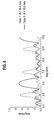
- FIG. 4 shows a 2.5 GHz clock signal received by a receiver on a circuit board without the non-uniform trace (dotted-line) and a 2.5 GHz clock signal received by a receiver on a circuit board having the non-uniform trace (straight line) according to some embodiments of the present invention.
- the signal received by the receiver on the circuit board including the non-uniform trace 254 has an improved gain (e.g., greater amplitude) than that of the signal received by the receiver on the circuit board without the non-uniform trace.
- FIG. 5 shows an eye-diagram of a 5Gbps pseudorandom binary sequence (PRBS) data sequence received by a receiver on a circuit board without the non-uniform trace (gray area), and received by a receiver on a circuit board having the non-uniform trace (black area) according to some embodiments of the present invention.
- PRBS pseudorandom binary sequence
- the opening of the eye for the signal received by the receiver having the non-uniform trace 254 has a larger height H1 than the height H2 of the opening of the eye for the signal received by the receiver without the non-uniform trace.
- the reflection of the signal may be enhanced at particular frequencies according to the period length ⁇ .
- FIG. 6 is a graph illustrating reflective spectrums of non-uniform traces having various period lengths ⁇ according to some embodiments of the present invention.
- FIG. 6 shows, for example, the reflective spectrums of differential microstrip traces fabricated on a standard FR4 graded material having a dielectric constant of about 4.0 and a loss tangent of about 0.02.
- Case 1 (dotted-line) has a period length ⁇ of about 36mm
- case 2 (straight line) has a period length ⁇ of about 18mm.
- Each of the non-uniform traces have 4 periods and includes two rectangular shapes, similar to that shown, for example, in FIG. 3A .
- the first portion has a smaller width than that of the second portion, and has a differential impedance of about 100 ⁇ .
- the second portion has a larger width than that of the first portion, and has a differential impedance ⁇ 100 ⁇ .
- differential impedance of the first and second portions are not limited thereto, and the differential impedance of the first and second portions may be set to any suitable differential impedance.
- suitable differential impedances of the first and second portions may be determined by rigorous channel simulations.
- the reflection of the signal by the non-uniform trace 254 having varying widths may be enhanced at particular frequencies based on the period length ⁇ .
- case 1 having the period length ⁇ of about 36mm exhibits greater reflection at frequencies of 2.5 GHz, 7.5 GHz, 12.5 GHz, etc., while having small or minimal reflection at the other frequencies
- case 2 having the period length ⁇ of about 18mm exhibits greater reflection at frequencies of 5 GHz, 15 GHz, etc., while having small or minimal reflection at the other frequencies.
- frequency-selective reflection patterns may be enhanced according to the period length ⁇ of the non-uniform trace 254 having the varying widths.
- channel loss may be compensated for by modifying the original channel on the circuit board to include the non-uniform trace 254 at or near the input of the receiver chip, without additional circuitry in either the transmitter chip or the receiver chip.
- the non-uniform trace 254 includes a plurality of periods each having a length and varying widths along different sections of the length. Each period selectively reflects the signal propagating through the channel at particular frequencies, which in the aggregate, enhances the signal at those frequencies, while having small or minimal reflection at other frequencies.
- the quality of the signal received by the receiver chip may be improved by emphasizing reflection for the selected frequencies at the input of the receiver chip.
Landscapes
- Engineering & Computer Science (AREA)
- Microelectronics & Electronic Packaging (AREA)
- Physics & Mathematics (AREA)
- Computer Hardware Design (AREA)
- General Physics & Mathematics (AREA)
- Theoretical Computer Science (AREA)
- Structure Of Printed Boards (AREA)
- Dc Digital Transmission (AREA)
- Printing Elements For Providing Electric Connections Between Printed Circuits (AREA)
- Cable Transmission Systems, Equalization Of Radio And Reduction Of Echo (AREA)
- Electroluminescent Light Sources (AREA)
- Planar Illumination Modules (AREA)
Abstract
Description
- This utility patent application claims priority to
U.S. Provisional Patent Application Serial No. 61/912,472, filed December 5, 2013 - Channel loss is a primary limiting factor when transmitting electrical signals over long distances at multi-Gbps data rates. Existing solutions focus on equalization schemes inside the transmitter and receiver chips, such as finite impulse response filters (FIRs), continuous time linear equalizers (CTLEs), and decision feedback equalizers (DFEs). However, these chip-level solutions are process technology dependent, have relatively high power consumption, and have performance variation across different process, voltage, and temperature (PVT) corners.
- The above information disclosed in this Background section is only for enhancement of understanding of the background of the invention and therefore it may contain information that does not form the prior art that is already known to a person of ordinary skill in the art.
- Aspects of embodiments of the present invention relate to a data channel for increasing the quality of received signals.
- According to an embodiment of the present invention, a display device includes: a display; a transmitter coupled to the display; a receiver coupled to the transmitter; and a trace coupled between the transmitter and the receiver, the trace including: a plurality of first portions; and a plurality of second portions alternately coupled in series with the first portions, the second portions having a width that is different from that of the first portions.
- The width of a first portion from among the first portions may be constant from a first end of the first portion to a second end of the first portion, and the width of a second portion from among the second portions may be constant from a first end of the second portion to a second end of the second portion.
- The width of a first portion from among the first portions may be smaller than the width of a second portion from among the second portions, and the width of the first portion may increase from a first end of the first portion to a second end of the first portion, and the width of the second portion may increase from a first end of the second portion to a second end of the second portion.
- The width of a first portion from among the first portions may be larger than the width of a second portion from among the second portions, and the width of the first portion may decrease from a first end of the first portion to a second end of the first portion, and the width of the second portion may decrease from a first end of the second portion to a second end of the second portion.
- The trace may include a plurality of periods, each of the periods may include one of the first portions and an adjacent one of the second portions, and a length of each of the periods may be equal to each other.
- According to another embodiment of the present invention, a circuit board includes: a first terminal to be coupled to a transmitter; a second terminal to be coupled to a receiver; and a trace coupled between the first terminal and the second terminal, the trace including: a plurality of first portions; and a plurality of second portions alternately coupled in series with the first portions, the second portions having a width that is different from that of the first portions.
- The width of a first portion from among the first portions may be constant from a first end of the first portion to a second end of the first portion, and the width of a second portion from among the second portions may be constant from a first end of the second portion to a second end of the second portion.
- The width of a first portion from among the first portions may be smaller than the width of a second portion from among the second portions, and the width of the first portion may increase from a first end of the first portion to a second end of the first portion, and the width of the second portion may increase from a first end of the second portion to a second end of the second portion.
- The width of a first portion from among the first portions may be larger than the width of a second portion from among the second portions, and the width of the first portion may decrease from a first end of the first portion to a second end of the first portion, and the width of the second portion may decrease from a first end of the second portion to a second end of the second portion.
- The trace may include a plurality of periods, each of the periods may include one of the first portions and an adjacent one of the second portions, and a length of each of the periods may be equal to each other.
- According to another embodiment of the present invention, a trace to be coupled to an input of a receiver includes: a plurality of first portions; and a plurality of second portions alternately coupled in series with the first portions, the second portions having a width that is different from that of the first portions.
- The width of a first portion from among the first portions may be constant from a first end of the first portion to a second end of the first portion, and the width of a second portion from among the second portions may be constant from a first end of the second portion to a second end of the second portion.
- Each one of the first portions and the second portions may have a quadrilateral shape.
- The width of a first portion from among the first portions may be smaller than the width of a second portion from among the second portions, and the width of the first portion may increase from a first end of the first portion to a second end of the first portion, and the width of the second portion may increase from a first end of the second portion to a second end of the second portion.
- Each one of the first portions and the second portions may have a trapezoidal shape or any suitable shape.
- The width of a first portion from among the first portions may be larger than the width of a second portion from among the second portions, and the width of the first portion may decrease from a first end of the first portion to a second end of the first portion, and the width of the second portion may decrease from a first end of the second portion to a second end of the second portion.
- Each one of the first portions and the second portions may have a trapezoidal shape or any suitable shape.
- The trace may further include a plurality of periods, each of the periods may include one of the first portions and an adjacent one of the second portions, and a length of each of the periods may be equal to each other.
- Each of the first portions may have a quadrilateral shape, each of the second portions may have a quadrilateral shape, and the width of the first portions may be smaller than the width of the second portions.
- Each of the periods may have a trapezoidal shape or any suitable shape.
- The above and other aspects and features of the present invention will become apparent to those skilled in the art from the following detailed description of the example embodiments with reference to the accompanying drawings.
-
FIG. 1 illustrates an example application of a non-uniform trace structure in the context of a display device according to some embodiments of the present invention. -
FIG. 2 is a schematic diagram illustrating a data lane for transmitting signals between devices, according to some embodiments of the present invention. -
FIGS. 3A and 3B are plan views illustrating various non-uniform trace structures included in the data lane shown inFIG. 2 , according to some embodiments of the present invention. -
FIG. 4 is a graph comparing received signals at a receiver through a channel including the non-uniform trace according to some embodiments of the present invention, and through a channel without the non-uniform trace. -
FIG. 5 is an eye-diagram comparing received pseudorandom data sequences at a receiver through a channel including the non-uniform trace according to some embodiments of the present invention, and through a channel without the non-uniform trace. -
FIG. 6 is a graph illustrating reflective spectrums of non-uniform traces having various period lengths according to some embodiments of the present invention. - Hereinafter, example embodiments will be described in more detail with reference to the accompanying drawings, in which like reference numbers refer to like elements throughout. The present invention, however, may be embodied in various different forms, and should not be construed as being limited to only the illustrated embodiments herein. Rather, these embodiments are provided as examples so that this disclosure will be thorough and complete, and will fully convey some of the aspects and features of the present invention to those skilled in the art. Accordingly, processes, elements, and techniques that are not necessary to those having ordinary skill in the art for a complete understanding of the aspects and features of the present invention are not described with respect to some of the embodiments of the present invention. Unless otherwise noted, like reference numerals denote like elements throughout the attached drawings and the written description, and thus, descriptions thereof will not be repeated. In the drawings, the relative sizes of elements, layers, and regions may be exaggerated for clarity.
- It will be understood that, although the terms "first," "second," "third," etc., may be used herein to describe various elements, components, regions, layers and/or sections, these elements, components, regions, layers and/or sections should not be limited by these terms. These terms are only used to distinguish one element, component, region, layer or section from another element, component, region, layer or section. Thus, a first element, component, region, layer or section described below could be termed a second element, component, region, layer or section, without departing from the scope of the present invention.
- Spatially relative terms, such as "beneath," "below," "lower," "under," "above," "upper," and the like, may be used herein for ease of explanation to describe one element or feature's relationship to another element(s) or feature(s) as illustrated in the figures. It will be understood that the spatially relative terms are intended to encompass different orientations of the device in use or in operation, in addition to the orientation depicted in the figures. For example, if the device in the figures is turned over, elements described as "below" or "beneath" or "under" other elements or features would then be oriented "above" the other elements or features. Thus, the example terms "below" and "under" can encompass both an orientation of above and below. The device may be otherwise oriented (e.g., rotated 90 degrees or at other orientations) and the spatially relative descriptors used herein should be interpreted accordingly. In addition, it will also be understood that when an element or layer is referred to as being "between" two elements or layers, it can be the only element or layer between the two elements or layers, or one or more intervening elements or layers may also be present.
- The terminology used herein is for the purpose of describing particular embodiments only and is not intended to be limiting of the present invention. As used herein, the singular forms "a," "an," and "the" are intended to include the plural forms as well, unless the context clearly indicates otherwise. It will be further understood that the terms "comprises" and/or "comprising," when used in this specification, specify the presence of the stated features, integers, steps, operations, elements, and/or components, but do not preclude the presence or addition of one or more other features, integers, steps, operations, elements, components, and/or groups thereof. As used herein, the term "and/or" includes any and all combinations of one or more of the associated listed items. Expressions such as "at least one of," when preceding a list of elements, modify the entire list of elements and do not modify the individual elements of the list. Further, the use of "may" when describing embodiments of the present invention refers to "one or more embodiments of the present invention." Also, the term "exemplary" is intended to refer to an example or illustration.
- It will be understood that when an element or layer is referred to as being "on," "connected to," or "coupled to" another element or layer, it can be directly on, connected to, or coupled to the other element or layer, or one or more intervening elements or layers may be present. However, when an element or layer is referred to as being "directly on," "directly connected to," or "directly coupled to" another element or layer, there are no intervening elements or layers present.
- Unless otherwise defined, all terms (including technical and scientific terms) used herein have the same meaning as commonly understood by one of ordinary skill in the art to which the present invention belongs. It will be further understood that terms, such as those defined in commonly used dictionaries, should be interpreted as having a meaning that is consistent with their meaning in the context of the relevant art and/or the present specification, and should not be interpreted in an idealized or overly formal sense, unless expressly so defined herein.
-
FIG. 1 illustrates an example application of a non-uniform trace structure in the context of a display device according to some embodiments of the present invention. - Referring to
FIG. 1 , adisplay device 100 includes atiming controller 110, ascan driver 120, adata driver 130, and a plurality of pixels Px in adisplay area 140. Each of the plurality of pixels Px is coupled to respective ones of the scan lines SL1 to SLn, where n is a positive integer, and data lines DL1 to DLj, where j is a positive integer, at crossing portions of the scan lines SL1 to SLn and the data lines DL1 to DLj. Each of the pixels Px receives a data signal from thedata driver 130 through the respective one of the data lines DL1 to DLj, when a scan signal is received from thescan driver 120 through a respective one of the scan lines SL1 to SLn. - The
timing controller 110 receives an image signal Image, a synchronization signal Sync, and a clock signal CLK from an external source (e.g., external to the timing controller). Thetiming controller 110 generates image data DATA, a data driver control signal DCS, and a scan driver control signal SCS. The synchronization signal Sync may include a vertical synchronization signal Vsync and a horizontal synchronization signal Hsync. - The
timing controller 110 is coupled to (e.g., connected to) thedata driver 130 and thescan driver 120 through respective ones of the data lanes 150 (e.g., data line, data path, data bus, etc.). Thetiming controller 110 transmits the image data Data and the data driver control signal DCS to thedata driver 130, and transmits the scan driver control signal SCS to thescan driver 120 through the respective ones of thedata lanes 150. Each of thedata lanes 150 according to embodiments of the present invention may have the same or substantially the same structure as any ones ofdata lanes 250 described in detail with reference toFIGS. 2 through 3B below. -
FIG. 2 is a schematic diagram illustrating an example of a data lane (e.g., thedata lane 150 shown inFIG. 1 ) for transmitting signals between devices, according to an embodiment of the present invention. - Referring to
FIG. 2 , a circuit orcircuit board 200 includes atransmitter 210, areceiver 220, and adata lane 250 coupling (e.g., connecting) thetransmitter 210 to thereceiver 220. Thecircuit board 200 may include any suitable circuit structure, for example, a printed circuit board (PCB) or a flexible printed circuit board (FPCB), but the present invention is not limited thereto. - The
data lane 250 includes achannel 252 for transmitting a signal (e.g., an electronic signal) from thetransmitter 210 to thereceiver 220, and a non-uniform trace 254 (e.g., a non-uniform trace having a grating-like structure) near (or at) a portion of thechannel 252 that is coupled to an input of thereceiver 220. As will be further discussed in detail below with reference toFIGS. 3A and 3B , thenon-uniform trace 254 enhances (e.g., selectively enhances) reflection of the signal propagating through thechannel 252 at particular frequencies (e.g., predetermined frequencies) to the input of thereceiver 220. - The
non-uniform trace 254 is terminated with a resistor R2 for reflection control, and to set a DC bias of the input of thereceiver 220. The resistor R2 may have the same or substantially the same impedance value as that of thechannel 252, and the input of thereceiver 220 may be left unterminated as shown inFIG. 2 . However, the present invention is not limited thereto. For example, the impedance of the resistor R2 may be any suitable impedance, and the input of thereceiver 220 may be terminated within the receiver chip as well. For example, the impedance of the resistor R2 may be experimentally determined based on a desired reflection property of thenon-uniform trace 254. If the input of thereceiver 220 is also terminated within the receiver chip, the reflection properties of thenon-uniform trace 254 may be fine-tuned with various different combinations of the impedance value of the resistor R2 and the impedance value of the terminated input within the receiver chip. -
FIGS. 3A and 3B are plan views illustrating various differentnon-uniform trace structures 254 included in thedata lane 250 shown inFIG. 2 , according to some embodiments of the present invention. - As shown in
FIGS. 3A and 3B , thenon-uniform trace 254 includes a plurality of periods r1 through r4. The number of periods may determine the amplitude of the reflected frequency. For example, a greater number of periods, may increase the resonance peak of the transmitted signal.FIGS. 3A and 3B show four periods r1 through r4, but the present invention is not limited thereto, and the number of periods may vary according to a desired depth of the ratio between the peak of the reflected frequency and the length of the frequency, as well as an amount of physical space available within thecircuit board 200. - Referring to
FIG. 3A , according to some embodiments, each of the periods r1 through r4 has a length Λ (e.g., a physical length) and a plurality of widths along a direction perpendicular to the length Λ. Accordingly, for each period, the width of the periods of thenon-uniform trace 254 may vary at different sections along the length Λ. In some embodiments, the length Λ of each period r1 through r4 may be equal to or substantially equal to each other, but the present invention is not limited thereto. - According to one embodiment, each of the periods r1 through r4 includes a first portion 301 a, a
second portion 303a opposite the first portion 301 a, and amiddle portion 302a coupling (e.g., connecting or between) the first portion 301 a and thesecond portion 303a. A width W1 of the first portion 301 a is different from (e.g., less than) a width W2 of thesecond portion 303a. The width W1 of the first portion 301 a may be constant or substantially constant from a first end of the first portion 301 a to a second end of the first portion 301 a, and the width W2 of thesecond portion 303a may be constant or substantially constant from a first end of thesecond portion 303a to a second end of thesecond portion 303a. However, the present invention is not limited thereto. - In some embodiments, a plurality of second portions may be alternately coupled in series with a plurality of first portions. For example, the first portion 301 a of the second period r2 is coupled to the
second portion 303a of the first period r1, and the first portions 301 a of each subsequent period are coupled to thesecond portions 303a of respective previous periods to form thenon-uniform trace 254. - In some embodiments, the first portion 301a may have a quadrilateral shape including four right angles and four sides. Two of the sides that are parallel to each other may extend in a first direction and may each have a height equal to the width W1. Two of the other sides that are parallel to each other may extend in a second direction and may each have a length equal to a first length λ1. The first length λ1 may be greater than the width W1. The first direction may extend along the width W1 direction and the second direction may extend along the length Λ direction. However, the present invention is not limited thereto, for example, the quadrilateral shape may include no right angles and/or each of the four sides may be equal in length to each other.
- In some embodiments, the
second portion 303a may have a quadrilateral shape including four right angles and four sides. Two of the sides that are parallel to each other may extend in the first direction and may each have a height equal to the width W2. Two of the other sides that are parallel to each other may extend in the second direction and may each have a length equal to a second length λ2. The second length λ2 may be greater than the width W2. However, the present invention is not limited thereto, for example, the quadrilateral shape may include no right angles and/or each of the four sides may be equal in length to each other. - In one embodiment, the first length λ1 may be equal to or substantially equal to the second length λ2. However, the present invention is not limited thereto, and the first length λ1 may be less than the second length λ2, or the first length λ1 may be greater than the second length λ2.
- The
middle portion 302a includes at least one location where the width varies. That is, themiddle portion 302a according to some embodiments of the present invention may include one or more step portions at which the width varies, but as will be described further below with reference toFIG. 3B , the present invention is not limited thereto. - In some embodiments, the
middle portion 302a may be a section along the length Λ where the width W1 of thefirst portion 302a and the width W2 of thesecond portion 303a meet. -
FIG. 3A shows that the width W1 of the first portion 301 a is smaller than the width W2 of thesecond portion 303a, but the present invention is not limited thereto, and the width of the first portion 301 a may be larger than the width of thesecond portion 303a depending on whether or not a positive reflection or a negative reflection is desired for the particular application. For example, if the first portion 301 a has a larger width W1 than that of W2 thesecond portion 303a, the reflection at the period (e.g., at a first end of the period) may be negative, whereas if the first portion 301a has a smaller width W1 than that of W2 thesecond portion 303a, then the reflection at the period (e.g., the first end of the period) may be positive. - Hereinafter, a
non-uniform trace structure 254 will be described according to another embodiment of the present invention with reference toFIG. 3B . Referring toFIG. 3B , according to another embodiment, each of the periods r1 through r4 has a length Λ (e.g., a physical length) and a plurality of widths along a direction perpendicular to the length Λ. Accordingly, for each period, the width of the periods of thenon-uniform trace 254 may gradually (e.g., continuously) vary along the length Λ. In some embodiments, the length Λ of each period r1 through r4 may be equal to or substantially equal to one another, but the present invention is not limited thereto. - According to one embodiment, each of the periods r1 through r4 includes a
first portion 301 b, asecond portion 303b opposite thefirst portion 301 b, and amiddle portion 302b coupling (e.g., connecting or between) thefirst portion 301 b and thesecond portion 303b. A width W3 of thefirst portion 301 b is different from (e.g., less than) a width W4 of thesecond portion 303b. - In some embodiments, a plurality of second portions may be alternately coupled in series with a plurality of first portions. For example, the
first portion 301 b of the second period r2 is coupled to thesecond portion 303b of the first period r1, and thefirst portions 301 b of each subsequent period is coupled to thesecond portions 303b of respective previous periods to form thenon-uniform trace 254. - In some embodiments, the
first portion 301 b may have a width that increases from a first end of thefirst portion 301 b to a second end of thefirst portion 301 b, and thesecond portion 303b may have a width that increases from a first end of thesecond portion 303b to a second end of thesecond portion 303b. However, the present invention is not limited thereto, for example, thefirst portion 301 b may have a width that decreases from the first end of thefirst portion 301 b to the second end of thefirst portion 301 b, and thesecond portion 303b may have a width that decreases from the first end of thesecond portion 303b to the second end of thesecond portion 303b. - In some embodiments, the
first portion 301b may be a trapezoidal shape and thesecond portion 303b may be a trapezoidal shape. However, the present invention is not limited thereto, and the first andsecond portions first portion 301 b may have a triangular shape and thesecond portion 303b may have a trapezoidal shape. If the period has a circular shape, then thefirst portion 301 b may be a semi-circle and thesecond portion 303b may be a semi-circle. - In some embodiments, the
first portion 301 b may be a section along the length Λ having the width W3. - In some embodiments, the
second portion 303b may be a section along the length Λ having the width W4. - In some embodiments, the
middle portion 302b includes at least one location where the width varies. That is, themiddle portion 302b according to some embodiments of the present invention may include one or more portions at which the width varies continuously or gradually, but the present invention is not limited thereto. - In some embodiments, the
middle portion 302b may extend from thefirst portion 301 b to thesecond portion 303b. Themiddle portion 302b may include a first slope gradually (e.g., continuously) increasing from thefirst portion 301 b to thesecond portion 303b, and may include a second slope gradually (e.g., continuously) decreasing from thefirst portion 301 b to thesecond portion 303b. The first slope may be a mirror image of the second slope along an axis intersecting center points of the width W3 and the width W4 that is parallel to the length Λ, but the present invention is not limited thereto. -
FIG. 3B shows that the width of thefirst portion 301 b is smaller than the width of thesecond portion 303b, but the present invention is not limited thereto, and the width of thefirst portion 301 b may be larger than the width of thesecond portion 303b depending on whether or not a positive reflection or a negative reflection is desired based on the particular application. For example, if thefirst portion 301 b has a larger width than that of thesecond portion 303b, the reflection at the period (e.g., at a first end of the period) may be negative, whereas if thefirst portion 301 b has a smaller width than that of thesecond portion 303b, then the reflection at the period (e.g., at the first end of the period) may be positive. - As shown in
FIG. 3A , the width of each period r1 through r4 may vary abruptly at one or more sections along the length Λ of each period r1 through r4, or as shown inFIG. 3B the width of each period r1 through r4 may gradually (e.g., continuously) vary at multiple sections along the length Λ of each period r1 through r4. Further,FIG. 3A shows each of the periods r1 through r4 including two rectangular shapes having different widths W1 and W2, andFIG. 3B shows each of the periods r1 through r4 including a single trapezium shape in which the width gradually (e.g., continuously) increases from the width W3 to the width W4. However, the manner in which the widths vary and the shape or shapes of the periods are not limited thereto, as long as the width varies at at least one section along the length Λ within each of the periods, so that there is reflection at each period. For example, the shape(s) of the periods may include any suitable shape(s) (e.g., a triangle shape, a star shape, a diamond shape, a circle shape, etc.) in which the width(s) of the period varies at at least one section along the length Λ. - Accordingly, the
non-uniform trace 254 includes a plurality of periods, each period including a length and a plurality of widths at different sections along the length. - As will be described in further detail below, when the signal propagates through the
channel 252, the signal is reflected at particular frequencies by thenon-uniform trace 254. That is, each period r1 through r4 of thenon-uniform trace 254 reflects the signal at particular frequencies according to the period's length Λ and varying widths. Thus, by arranging the periods having the varying widths according to its length Λ, the reflection at each period is combined such that a strong reflection at particular frequencies is enhanced, while having small or minimal reflection at other frequencies. - Accordingly, unlike uniform traces, the
non-uniform trace 254 having the plurality of periods with the varying widths allow strong reflection at particular frequencies through constructive interference of multi-path reflection signals. For example, an overall quality of a received signal can benefit from reflection, when the reflection of the signal is more significant at frequencies near a clock rate of the channel than at lower frequencies. - A total reflection of the
non-uniform trace 254 peaks at a frequency f defined by equation (1) below, when individual reflections from each period r1 through r4 are in phase with one another.
In equation (1), Λ is the physical length of each period, Veff is the effective signal propagation speed in each period, and n is an integer greater than or equal to 0 (n>=0). - Thus, as further described in detail with reference to
FIGS. 4 and5 , thechannel 252 including thenon-uniform trace 254 as shown inFIGS. 2 ,3A, and 3B , enhances the quality of the signal received by thereceiver 220 of both clock signals and arbitrary data sequences transmitted by thetransmitter 210 when compared to a channel without the non-uniform trace. -
FIGS. 4 and5 are graphs comparing the improvement of a signal received by a receiver on a circuit board having thenon-uniform trace 254 according to some embodiments of the present invention, and to a circuit board without the non-uniform trace. - Referring to
FIGS. 4 and5 , in some embodiments, more than 80% improvement is achieved for a differential link operating at, for example, 5Gb/s. The original channel on the circuit board is 600mm long, and the non-uniform trace includes 4 periods, each period being 36mm long. -
FIG. 4 shows a 2.5 GHz clock signal received by a receiver on a circuit board without the non-uniform trace (dotted-line) and a 2.5 GHz clock signal received by a receiver on a circuit board having the non-uniform trace (straight line) according to some embodiments of the present invention. As shown inFIG. 4 , the signal received by the receiver on the circuit board including thenon-uniform trace 254 has an improved gain (e.g., greater amplitude) than that of the signal received by the receiver on the circuit board without the non-uniform trace. -
FIG. 5 shows an eye-diagram of a 5Gbps pseudorandom binary sequence (PRBS) data sequence received by a receiver on a circuit board without the non-uniform trace (gray area), and received by a receiver on a circuit board having the non-uniform trace (black area) according to some embodiments of the present invention. As shown inFIG. 5 , the opening of the eye for the signal received by the receiver having thenon-uniform trace 254 has a larger height H1 than the height H2 of the opening of the eye for the signal received by the receiver without the non-uniform trace. - As will be described further below with reference to
FIG. 6 , the reflection of the signal may be enhanced at particular frequencies according to the period length Λ. -
FIG. 6 is a graph illustrating reflective spectrums of non-uniform traces having various period lengths Λ according to some embodiments of the present invention. -
FIG. 6 shows, for example, the reflective spectrums of differential microstrip traces fabricated on a standard FR4 graded material having a dielectric constant of about 4.0 and a loss tangent of about 0.02. Case 1 (dotted-line) has a period length Λ of about 36mm, and case 2 (straight line) has a period length Λ of about 18mm. Each of the non-uniform traces have 4 periods and includes two rectangular shapes, similar to that shown, for example, inFIG. 3A . The first portion has a smaller width than that of the second portion, and has a differential impedance of about 100Ω. The second portion has a larger width than that of the first portion, and has a differential impedance < 100Ω. However, the differential impedance of the first and second portions are not limited thereto, and the differential impedance of the first and second portions may be set to any suitable differential impedance. For example, suitable differential impedances of the first and second portions may be determined by rigorous channel simulations. - As shown in
FIG. 6 , according to some embodiments, the reflection of the signal by thenon-uniform trace 254 having varying widths may be enhanced at particular frequencies based on the period length Λ. For example,case 1 having the period length Λ of about 36mm exhibits greater reflection at frequencies of 2.5 GHz, 7.5 GHz, 12.5 GHz, etc., while having small or minimal reflection at the other frequencies, whereascase 2 having the period length Λ of about 18mm exhibits greater reflection at frequencies of 5 GHz, 15 GHz, etc., while having small or minimal reflection at the other frequencies. Thus, frequency-selective reflection patterns may be enhanced according to the period length Λ of thenon-uniform trace 254 having the varying widths. - Accordingly, in some embodiments of the present invention, channel loss may be compensated for by modifying the original channel on the circuit board to include the
non-uniform trace 254 at or near the input of the receiver chip, without additional circuitry in either the transmitter chip or the receiver chip. Thenon-uniform trace 254 includes a plurality of periods each having a length and varying widths along different sections of the length. Each period selectively reflects the signal propagating through the channel at particular frequencies, which in the aggregate, enhances the signal at those frequencies, while having small or minimal reflection at other frequencies. Thus, the quality of the signal received by the receiver chip may be improved by emphasizing reflection for the selected frequencies at the input of the receiver chip. - Although the present invention has been described with reference to the example embodiments, those skilled in the art will recognize that various changes and modifications to the described embodiments may be performed, all without departing from the spirit and scope of the present invention. Furthermore, those skilled in the various arts will recognize that the present invention described herein will suggest solutions to other tasks and adaptations for other applications. It is the applicant's intention to cover by the claims herein, all such uses of the present invention, and those changes and modifications which could be made to the example embodiments of the present invention herein chosen for the purpose of disclosure, all without departing from the scope of the present invention. Thus, the example embodiments of the present invention should be considered in all respects as illustrative and not restrictive, with the scope of the present invention being indicated by the appended claims and their equivalents.
Claims (20)
- A display device comprising:a display;a transmitter coupled to the display;a receiver coupled to the transmitter; anda trace coupled between the transmitter and the receiver, the trace comprising:a plurality of first portions; anda plurality of second portions alternately coupled in series with the first portions, the second portions having a width that is different from that of the first portions.
- The display device of claim 1, wherein the width of a first portion from among the first portions is constant from a first end of the first portion to a second end of the first portion, and
the width of a second portion from among the second portions is constant from a first end of the second portion to a second end of the second portion. - The display device of claim 1, wherein the width of a first portion from among the first portions is smaller than the width of a second portion from among the second portions, and
the width of the first portion increases from a first end of the first portion to a second end of the first portion, and the width of the second portion increases from a first end of the second portion to a second end of the second portion. - The display device of claim 1, wherein the width of a first portion from among the first portions is larger than the width of a second portion from among the second portions, and
the width of the first portion decreases from a first end of the first portion to a second end of the first portion, and the width of the second portion decreases from a first end of the second portion to a second end of the second portion. - The display device of one of the claims 1-4, wherein the trace comprises a plurality of periods, each of the periods comprising one of the first portions and an adjacent one of the second portions, and a length of each of the periods is equal to each other.
- A circuit board comprising:a first terminal to be coupled to a transmitter;a second terminal to be coupled to a receiver; anda trace coupled between the first terminal and the second terminal, the trace comprising:a plurality of first portions; anda plurality of second portions alternately coupled in series with the first portions, the second portions having a width that is different from that of the first portions.
- The circuit board of claim 6, wherein the width of a first portion from among the first portions is constant from a first end of the first portion to a second end of the first portion, and
the width of a second portion from among the second portions is constant from a first end of the second portion to a second end of the second portion. - The circuit board of claim 6, wherein the width of a first portion from among the first portions is smaller than the width of a second portion from among the second portions, and
the width of the first portion increases from a first end of the first portion to a second end of the first portion, and the width of the second portion increases from a first end of the second portion to a second end of the second portion. - The circuit board of claim 6, wherein the width of a first portion from among the first portions is larger than the width of a second portion from among the second portions, and
the width of the first portion decreases from a first end of the first portion to a second end of the first portion, and the width of the second portion decreases from a first end of the second portion to a second end of the second portion. - The circuit board of claim 6, wherein the trace comprises a plurality of periods, each of the periods comprising one of the first portions and an adjacent one of the second portions, and a length of each of the periods is equal to each other.
- A trace to be coupled to an input of a receiver, the trace comprising:a plurality of first portions; anda plurality of second portions alternately coupled in series with the first portions, the second portions having a width that is different from that of the first portions.
- The trace of claim 11, wherein the width of a first portion from among the first portions is constant from a first end of the first portion to a second end of the first portion, and
the width of a second portion from among the second portions is constant from a first end of the second portion to a second end of the second portion. - The trace of claim 11 or 12, wherein each one of the first portions and the second portions have a quadrilateral shape.
- The trace of claim 11, wherein the width of a first portion from among the first portions is smaller than the width of a second portion from among the second portions, and
the width of the first portion increases from a first end of the first portion to a second end of the first portion, and the width of the second portion increases from a first end of the second portion to a second end of the second portion. - The trace of claim 14, wherein each one of the first portions and the second portions have a trapezoidal shape.
- The trace of claim 11, wherein the width of a first portion from among the first portions is larger than the width of a second portion from among the second portions, and
the width of the first portion decreases from a first end of the first portion to a second end of the first portion, and the width of the second portion decreases from a first end of the second portion to a second end of the second portion. - The trace of claim 16, wherein each one of the first portions and the second portions have a trapezoidal shape.
- The trace of one of the claims 11-17 further comprising a plurality of periods, each of the periods comprising one of the first portions and an adjacent one of the second portions, and a length of each of the periods is equal to each other.
- The trace of claim 18, wherein each of the first portions have a quadrilateral shape, each of the second portions have a quadrilateral shape, and the width of the first portions is smaller than the width of the second portions.
- The trace of claim 18, wherein each of the periods have a trapezoidal shape.
Applications Claiming Priority (2)
| Application Number | Priority Date | Filing Date | Title |
|---|---|---|---|
| US201361912472P | 2013-12-05 | 2013-12-05 | |
| US14/535,216 US9595217B2 (en) | 2013-12-05 | 2014-11-06 | Trace structure for improved electrical signaling |
Publications (2)
| Publication Number | Publication Date |
|---|---|
| EP2882266A1 true EP2882266A1 (en) | 2015-06-10 |
| EP2882266B1 EP2882266B1 (en) | 2023-05-17 |
Family
ID=52231801
Family Applications (1)
| Application Number | Title | Priority Date | Filing Date |
|---|---|---|---|
| EP14196024.5A Active EP2882266B1 (en) | 2013-12-05 | 2014-12-03 | Trace structure for improved electrical signaling |
Country Status (6)
| Country | Link |
|---|---|
| US (1) | US9595217B2 (en) |
| EP (1) | EP2882266B1 (en) |
| JP (1) | JP6574566B2 (en) |
| KR (1) | KR102240292B1 (en) |
| CN (1) | CN104765583B (en) |
| TW (1) | TWI636443B (en) |
Families Citing this family (5)
| Publication number | Priority date | Publication date | Assignee | Title |
|---|---|---|---|---|
| KR102548857B1 (en) * | 2016-11-30 | 2023-06-29 | 삼성디스플레이 주식회사 | Display apparatus and method of driving display panel using the same |
| US10667384B2 (en) * | 2018-07-17 | 2020-05-26 | Quanta Computer Inc. | Low frequency reduced passive equalizer |
| CN112150954B (en) * | 2019-06-27 | 2024-09-20 | 奇景光电股份有限公司 | Electronic device |
| CN113645751B (en) * | 2021-07-26 | 2023-05-26 | 合肥联宝信息技术有限公司 | Signal line and anti-interference structure determining method and device |
| WO2025102272A1 (en) * | 2023-11-15 | 2025-05-22 | 鸿富锦精密工业(武汉)有限公司 | Circuit board assembly and electronic device |
Citations (5)
| Publication number | Priority date | Publication date | Assignee | Title |
|---|---|---|---|---|
| GB1131115A (en) * | 1966-06-13 | 1968-10-23 | Marconi Co Ltd | Improvements in or relating to transmission line and wave guide impedance matching arrangements |
| EP1326302A2 (en) * | 2001-12-28 | 2003-07-09 | Zarlink Semiconductor (U.S.) Inc. | Integrated circuit fractal antenna in a hearing aid device |
| US20040125526A1 (en) * | 2002-12-30 | 2004-07-01 | Motorola, Inc. | Distributive capacitor for high density applications |
| US20090152689A1 (en) * | 2007-12-17 | 2009-06-18 | Agere Systems Inc. | Integrated Circuit Package for High-Speed Signals |
| US20090195327A1 (en) * | 2008-01-31 | 2009-08-06 | Taiwan Semiconductor Manufacturing Company, Ltd. | Transmitting radio frequency signal in semiconductor structure |
Family Cites Families (16)
| Publication number | Priority date | Publication date | Assignee | Title |
|---|---|---|---|---|
| US6459343B1 (en) | 1999-02-25 | 2002-10-01 | Formfactor, Inc. | Integrated circuit interconnect system forming a multi-pole filter |
| KR20020054900A (en) | 2000-12-28 | 2002-07-08 | 박종섭 | Printer circuit board for memory module |
| TWI254903B (en) * | 2004-02-27 | 2006-05-11 | Au Optronics Corp | Terminal circuit of liquid crystal display and manufacturing method therefor |
| KR100691583B1 (en) * | 2004-12-31 | 2007-03-09 | 학교법인 포항공과대학교 | Multi-drop bus structure memory system with multiple termination resistors |
| JP2006250986A (en) * | 2005-03-08 | 2006-09-21 | Sanyo Epson Imaging Devices Corp | Drive circuit of electro-optical device, electro-optical device, and electronic equipment provided with it |
| JP2007012661A (en) | 2005-06-28 | 2007-01-18 | Seiko Epson Corp | Flexible printed circuit board, mounting structure, droplet discharge head |
| KR101249833B1 (en) | 2006-09-06 | 2013-04-05 | 삼성전자주식회사 | Pcb with low emi noise |
| US7564695B2 (en) | 2007-07-09 | 2009-07-21 | Canon Kabushiki Kaisha | Circuit connection structure and printed circuit board |
| KR101580897B1 (en) | 2008-10-07 | 2015-12-30 | 삼성전자주식회사 | Display driver method thereof and device having the display driver |
| CN101944315B (en) * | 2009-07-09 | 2014-04-02 | 奇景光电股份有限公司 | Source driver and display using the source driver |
| TWI419620B (en) | 2010-05-20 | 2013-12-11 | Hon Hai Prec Ind Co Ltd | Printed circuit board |
| JP2012227793A (en) * | 2011-04-20 | 2012-11-15 | Univ Of Electro-Communications | Transmission line resonator and bandpass filter, balanced filter, push-push generator and splitter using the same |
| JP5246899B1 (en) * | 2012-06-07 | 2013-07-24 | 国立大学法人 筑波大学 | High-frequency wiring structure, high-frequency mounting substrate, high-frequency wiring structure manufacturing method, and high-frequency signal waveform shaping method |
| JP6216951B2 (en) | 2012-07-12 | 2017-10-25 | 学校法人慶應義塾 | Directional coupled communication device |
| KR102023939B1 (en) | 2012-12-26 | 2019-11-04 | 엘지디스플레이 주식회사 | Image display device and method for driving the same |
| KR102082936B1 (en) * | 2013-10-21 | 2020-04-14 | 엘지디스플레이 주식회사 | Touch sensing system and driving method thereof |
-
2014
- 2014-11-06 US US14/535,216 patent/US9595217B2/en active Active
- 2014-12-03 EP EP14196024.5A patent/EP2882266B1/en active Active
- 2014-12-03 JP JP2014244763A patent/JP6574566B2/en active Active
- 2014-12-03 TW TW103141991A patent/TWI636443B/en active
- 2014-12-05 KR KR1020140174442A patent/KR102240292B1/en active Active
- 2014-12-05 CN CN201410738760.2A patent/CN104765583B/en active Active
Patent Citations (5)
| Publication number | Priority date | Publication date | Assignee | Title |
|---|---|---|---|---|
| GB1131115A (en) * | 1966-06-13 | 1968-10-23 | Marconi Co Ltd | Improvements in or relating to transmission line and wave guide impedance matching arrangements |
| EP1326302A2 (en) * | 2001-12-28 | 2003-07-09 | Zarlink Semiconductor (U.S.) Inc. | Integrated circuit fractal antenna in a hearing aid device |
| US20040125526A1 (en) * | 2002-12-30 | 2004-07-01 | Motorola, Inc. | Distributive capacitor for high density applications |
| US20090152689A1 (en) * | 2007-12-17 | 2009-06-18 | Agere Systems Inc. | Integrated Circuit Package for High-Speed Signals |
| US20090195327A1 (en) * | 2008-01-31 | 2009-08-06 | Taiwan Semiconductor Manufacturing Company, Ltd. | Transmitting radio frequency signal in semiconductor structure |
Also Published As
| Publication number | Publication date |
|---|---|
| TWI636443B (en) | 2018-09-21 |
| EP2882266B1 (en) | 2023-05-17 |
| CN104765583A (en) | 2015-07-08 |
| KR102240292B1 (en) | 2021-04-14 |
| US20150161929A1 (en) | 2015-06-11 |
| JP6574566B2 (en) | 2019-09-11 |
| JP2015128289A (en) | 2015-07-09 |
| KR20150065617A (en) | 2015-06-15 |
| CN104765583B (en) | 2019-09-17 |
| US9595217B2 (en) | 2017-03-14 |
| TW201539410A (en) | 2015-10-16 |
Similar Documents
| Publication | Publication Date | Title |
|---|---|---|
| EP2882266A1 (en) | Trace structure for improved electrical signaling | |
| CN207038050U (en) | Array base palte and display device | |
| US10325053B2 (en) | Triangular routing for high speed differential pair length matching | |
| US8384489B2 (en) | Serpentine micro-strip lines configured in an aggressor/victim type transmission line structure | |
| US7859309B2 (en) | Clock tree distributing method | |
| US10249989B2 (en) | Mitigation of connector stub resonance | |
| EP2874474A2 (en) | Crosstalk reduction in signal lines by crosstalk introduction | |
| US10153238B2 (en) | Electrical channel including pattern voids | |
| CN113473694A (en) | Wiring structure of PCB and PCB | |
| KR102382000B1 (en) | Clock channel, circuit board and electronic device indlucing transmission line | |
| CN108124375A (en) | Overcome the method for transmission line phase difference and its transmission wire wiring structure | |
| RU2696213C2 (en) | Circuit, display substrate and display device | |
| CN101569054B (en) | Apparatus and method for high speed signals on printed circuit boards | |
| US9069913B2 (en) | Circuit topology for multiple loads | |
| CN101001229A (en) | Loss compensation method | |
| CN104103392A (en) | Resistor arrangement device |
Legal Events
| Date | Code | Title | Description |
|---|---|---|---|
| PUAI | Public reference made under article 153(3) epc to a published international application that has entered the european phase |
Free format text: ORIGINAL CODE: 0009012 |
|
| 17P | Request for examination filed |
Effective date: 20141203 |
|
| AK | Designated contracting states |
Kind code of ref document: A1 Designated state(s): AL AT BE BG CH CY CZ DE DK EE ES FI FR GB GR HR HU IE IS IT LI LT LU LV MC MK MT NL NO PL PT RO RS SE SI SK SM TR |
|
| AX | Request for extension of the european patent |
Extension state: BA ME |
|
| RAP1 | Party data changed (applicant data changed or rights of an application transferred) |
Owner name: SAMSUNG DISPLAY CO., LTD. |
|
| R17P | Request for examination filed (corrected) |
Effective date: 20151203 |
|
| RBV | Designated contracting states (corrected) |
Designated state(s): AL AT BE BG CH CY CZ DE DK EE ES FI FR GB GR HR HU IE IS IT LI LT LU LV MC MK MT NL NO PL PT RO RS SE SI SK SM TR |
|
| STAA | Information on the status of an ep patent application or granted ep patent |
Free format text: STATUS: EXAMINATION IS IN PROGRESS |
|
| 17Q | First examination report despatched |
Effective date: 20180525 |
|
| GRAP | Despatch of communication of intention to grant a patent |
Free format text: ORIGINAL CODE: EPIDOSNIGR1 |
|
| STAA | Information on the status of an ep patent application or granted ep patent |
Free format text: STATUS: GRANT OF PATENT IS INTENDED |
|
| RIC1 | Information provided on ipc code assigned before grant |
Ipc: G09G 5/00 19900101ALN20230105BHEP Ipc: H01L 23/66 19900101ALN20230105BHEP Ipc: G09G 3/20 19800101ALI20230105BHEP Ipc: H05K 1/02 19680901AFI20230105BHEP |
|
| INTG | Intention to grant announced |
Effective date: 20230127 |
|
| RIC1 | Information provided on ipc code assigned before grant |
Ipc: G09G 5/00 20060101ALN20230117BHEP Ipc: H01L 23/66 20060101ALN20230117BHEP Ipc: G09G 3/20 20060101ALI20230117BHEP Ipc: H05K 1/02 20060101AFI20230117BHEP |
|
| GRAS | Grant fee paid |
Free format text: ORIGINAL CODE: EPIDOSNIGR3 |
|
| GRAA | (expected) grant |
Free format text: ORIGINAL CODE: 0009210 |
|
| STAA | Information on the status of an ep patent application or granted ep patent |
Free format text: STATUS: THE PATENT HAS BEEN GRANTED |
|
| AK | Designated contracting states |
Kind code of ref document: B1 Designated state(s): AL AT BE BG CH CY CZ DE DK EE ES FI FR GB GR HR HU IE IS IT LI LT LU LV MC MK MT NL NO PL PT RO RS SE SI SK SM TR |
|
| REG | Reference to a national code |
Ref country code: GB Ref legal event code: FG4D |
|
| REG | Reference to a national code |
Ref country code: CH Ref legal event code: EP |
|
| REG | Reference to a national code |
Ref country code: DE Ref legal event code: R096 Ref document number: 602014086960 Country of ref document: DE |
|
| REG | Reference to a national code |
Ref country code: IE Ref legal event code: FG4D |
|
| REG | Reference to a national code |
Ref country code: AT Ref legal event code: REF Ref document number: 1568942 Country of ref document: AT Kind code of ref document: T Effective date: 20230615 |
|
| P01 | Opt-out of the competence of the unified patent court (upc) registered |
Effective date: 20230516 |
|
| REG | Reference to a national code |
Ref country code: NL Ref legal event code: FP |
|
| REG | Reference to a national code |
Ref country code: LT Ref legal event code: MG9D |
|
| REG | Reference to a national code |
Ref country code: AT Ref legal event code: MK05 Ref document number: 1568942 Country of ref document: AT Kind code of ref document: T Effective date: 20230517 |
|
| PG25 | Lapsed in a contracting state [announced via postgrant information from national office to epo] |
Ref country code: SE Free format text: LAPSE BECAUSE OF FAILURE TO SUBMIT A TRANSLATION OF THE DESCRIPTION OR TO PAY THE FEE WITHIN THE PRESCRIBED TIME-LIMIT Effective date: 20230517 Ref country code: PT Free format text: LAPSE BECAUSE OF FAILURE TO SUBMIT A TRANSLATION OF THE DESCRIPTION OR TO PAY THE FEE WITHIN THE PRESCRIBED TIME-LIMIT Effective date: 20230918 Ref country code: NO Free format text: LAPSE BECAUSE OF FAILURE TO SUBMIT A TRANSLATION OF THE DESCRIPTION OR TO PAY THE FEE WITHIN THE PRESCRIBED TIME-LIMIT Effective date: 20230817 Ref country code: ES Free format text: LAPSE BECAUSE OF FAILURE TO SUBMIT A TRANSLATION OF THE DESCRIPTION OR TO PAY THE FEE WITHIN THE PRESCRIBED TIME-LIMIT Effective date: 20230517 Ref country code: AT Free format text: LAPSE BECAUSE OF FAILURE TO SUBMIT A TRANSLATION OF THE DESCRIPTION OR TO PAY THE FEE WITHIN THE PRESCRIBED TIME-LIMIT Effective date: 20230517 |
|
| PG25 | Lapsed in a contracting state [announced via postgrant information from national office to epo] |
Ref country code: RS Free format text: LAPSE BECAUSE OF FAILURE TO SUBMIT A TRANSLATION OF THE DESCRIPTION OR TO PAY THE FEE WITHIN THE PRESCRIBED TIME-LIMIT Effective date: 20230517 Ref country code: PL Free format text: LAPSE BECAUSE OF FAILURE TO SUBMIT A TRANSLATION OF THE DESCRIPTION OR TO PAY THE FEE WITHIN THE PRESCRIBED TIME-LIMIT Effective date: 20230517 Ref country code: LV Free format text: LAPSE BECAUSE OF FAILURE TO SUBMIT A TRANSLATION OF THE DESCRIPTION OR TO PAY THE FEE WITHIN THE PRESCRIBED TIME-LIMIT Effective date: 20230517 Ref country code: LT Free format text: LAPSE BECAUSE OF FAILURE TO SUBMIT A TRANSLATION OF THE DESCRIPTION OR TO PAY THE FEE WITHIN THE PRESCRIBED TIME-LIMIT Effective date: 20230517 Ref country code: IS Free format text: LAPSE BECAUSE OF FAILURE TO SUBMIT A TRANSLATION OF THE DESCRIPTION OR TO PAY THE FEE WITHIN THE PRESCRIBED TIME-LIMIT Effective date: 20230917 Ref country code: HR Free format text: LAPSE BECAUSE OF FAILURE TO SUBMIT A TRANSLATION OF THE DESCRIPTION OR TO PAY THE FEE WITHIN THE PRESCRIBED TIME-LIMIT Effective date: 20230517 Ref country code: GR Free format text: LAPSE BECAUSE OF FAILURE TO SUBMIT A TRANSLATION OF THE DESCRIPTION OR TO PAY THE FEE WITHIN THE PRESCRIBED TIME-LIMIT Effective date: 20230818 |
|
| PG25 | Lapsed in a contracting state [announced via postgrant information from national office to epo] |
Ref country code: FI Free format text: LAPSE BECAUSE OF FAILURE TO SUBMIT A TRANSLATION OF THE DESCRIPTION OR TO PAY THE FEE WITHIN THE PRESCRIBED TIME-LIMIT Effective date: 20230517 |
|
| PG25 | Lapsed in a contracting state [announced via postgrant information from national office to epo] |
Ref country code: SK Free format text: LAPSE BECAUSE OF FAILURE TO SUBMIT A TRANSLATION OF THE DESCRIPTION OR TO PAY THE FEE WITHIN THE PRESCRIBED TIME-LIMIT Effective date: 20230517 |
|
| PG25 | Lapsed in a contracting state [announced via postgrant information from national office to epo] |
Ref country code: SM Free format text: LAPSE BECAUSE OF FAILURE TO SUBMIT A TRANSLATION OF THE DESCRIPTION OR TO PAY THE FEE WITHIN THE PRESCRIBED TIME-LIMIT Effective date: 20230517 Ref country code: SK Free format text: LAPSE BECAUSE OF FAILURE TO SUBMIT A TRANSLATION OF THE DESCRIPTION OR TO PAY THE FEE WITHIN THE PRESCRIBED TIME-LIMIT Effective date: 20230517 Ref country code: RO Free format text: LAPSE BECAUSE OF FAILURE TO SUBMIT A TRANSLATION OF THE DESCRIPTION OR TO PAY THE FEE WITHIN THE PRESCRIBED TIME-LIMIT Effective date: 20230517 Ref country code: EE Free format text: LAPSE BECAUSE OF FAILURE TO SUBMIT A TRANSLATION OF THE DESCRIPTION OR TO PAY THE FEE WITHIN THE PRESCRIBED TIME-LIMIT Effective date: 20230517 Ref country code: DK Free format text: LAPSE BECAUSE OF FAILURE TO SUBMIT A TRANSLATION OF THE DESCRIPTION OR TO PAY THE FEE WITHIN THE PRESCRIBED TIME-LIMIT Effective date: 20230517 Ref country code: CZ Free format text: LAPSE BECAUSE OF FAILURE TO SUBMIT A TRANSLATION OF THE DESCRIPTION OR TO PAY THE FEE WITHIN THE PRESCRIBED TIME-LIMIT Effective date: 20230517 |
|
| REG | Reference to a national code |
Ref country code: DE Ref legal event code: R097 Ref document number: 602014086960 Country of ref document: DE |
|
| PLBE | No opposition filed within time limit |
Free format text: ORIGINAL CODE: 0009261 |
|
| STAA | Information on the status of an ep patent application or granted ep patent |
Free format text: STATUS: NO OPPOSITION FILED WITHIN TIME LIMIT |
|
| 26N | No opposition filed |
Effective date: 20240220 |
|
| PG25 | Lapsed in a contracting state [announced via postgrant information from national office to epo] |
Ref country code: SI Free format text: LAPSE BECAUSE OF FAILURE TO SUBMIT A TRANSLATION OF THE DESCRIPTION OR TO PAY THE FEE WITHIN THE PRESCRIBED TIME-LIMIT Effective date: 20230517 |
|
| PG25 | Lapsed in a contracting state [announced via postgrant information from national office to epo] |
Ref country code: SI Free format text: LAPSE BECAUSE OF FAILURE TO SUBMIT A TRANSLATION OF THE DESCRIPTION OR TO PAY THE FEE WITHIN THE PRESCRIBED TIME-LIMIT Effective date: 20230517 Ref country code: IT Free format text: LAPSE BECAUSE OF FAILURE TO SUBMIT A TRANSLATION OF THE DESCRIPTION OR TO PAY THE FEE WITHIN THE PRESCRIBED TIME-LIMIT Effective date: 20230517 |
|
| REG | Reference to a national code |
Ref country code: CH Ref legal event code: PL |
|
| PG25 | Lapsed in a contracting state [announced via postgrant information from national office to epo] |
Ref country code: LU Free format text: LAPSE BECAUSE OF NON-PAYMENT OF DUE FEES Effective date: 20231203 |
|
| PG25 | Lapsed in a contracting state [announced via postgrant information from national office to epo] |
Ref country code: MC Free format text: LAPSE BECAUSE OF FAILURE TO SUBMIT A TRANSLATION OF THE DESCRIPTION OR TO PAY THE FEE WITHIN THE PRESCRIBED TIME-LIMIT Effective date: 20230517 |
|
| REG | Reference to a national code |
Ref country code: BE Ref legal event code: MM Effective date: 20231231 |
|
| PG25 | Lapsed in a contracting state [announced via postgrant information from national office to epo] |
Ref country code: MC Free format text: LAPSE BECAUSE OF FAILURE TO SUBMIT A TRANSLATION OF THE DESCRIPTION OR TO PAY THE FEE WITHIN THE PRESCRIBED TIME-LIMIT Effective date: 20230517 Ref country code: LU Free format text: LAPSE BECAUSE OF NON-PAYMENT OF DUE FEES Effective date: 20231203 |
|
| REG | Reference to a national code |
Ref country code: IE Ref legal event code: MM4A |
|
| PG25 | Lapsed in a contracting state [announced via postgrant information from national office to epo] |
Ref country code: IE Free format text: LAPSE BECAUSE OF NON-PAYMENT OF DUE FEES Effective date: 20231203 |
|
| PG25 | Lapsed in a contracting state [announced via postgrant information from national office to epo] |
Ref country code: BE Free format text: LAPSE BECAUSE OF NON-PAYMENT OF DUE FEES Effective date: 20231231 |
|
| PG25 | Lapsed in a contracting state [announced via postgrant information from national office to epo] |
Ref country code: FR Free format text: LAPSE BECAUSE OF NON-PAYMENT OF DUE FEES Effective date: 20231231 |
|
| PG25 | Lapsed in a contracting state [announced via postgrant information from national office to epo] |
Ref country code: CH Free format text: LAPSE BECAUSE OF NON-PAYMENT OF DUE FEES Effective date: 20231231 |
|
| PG25 | Lapsed in a contracting state [announced via postgrant information from national office to epo] |
Ref country code: IE Free format text: LAPSE BECAUSE OF NON-PAYMENT OF DUE FEES Effective date: 20231203 Ref country code: FR Free format text: LAPSE BECAUSE OF NON-PAYMENT OF DUE FEES Effective date: 20231231 Ref country code: CH Free format text: LAPSE BECAUSE OF NON-PAYMENT OF DUE FEES Effective date: 20231231 Ref country code: BE Free format text: LAPSE BECAUSE OF NON-PAYMENT OF DUE FEES Effective date: 20231231 |
|
| PG25 | Lapsed in a contracting state [announced via postgrant information from national office to epo] |
Ref country code: BG Free format text: LAPSE BECAUSE OF FAILURE TO SUBMIT A TRANSLATION OF THE DESCRIPTION OR TO PAY THE FEE WITHIN THE PRESCRIBED TIME-LIMIT Effective date: 20230517 |
|
| PG25 | Lapsed in a contracting state [announced via postgrant information from national office to epo] |
Ref country code: BG Free format text: LAPSE BECAUSE OF FAILURE TO SUBMIT A TRANSLATION OF THE DESCRIPTION OR TO PAY THE FEE WITHIN THE PRESCRIBED TIME-LIMIT Effective date: 20230517 |
|
| PG25 | Lapsed in a contracting state [announced via postgrant information from national office to epo] |
Ref country code: CY Free format text: LAPSE BECAUSE OF FAILURE TO SUBMIT A TRANSLATION OF THE DESCRIPTION OR TO PAY THE FEE WITHIN THE PRESCRIBED TIME-LIMIT; INVALID AB INITIO Effective date: 20141203 |
|
| PG25 | Lapsed in a contracting state [announced via postgrant information from national office to epo] |
Ref country code: HU Free format text: LAPSE BECAUSE OF FAILURE TO SUBMIT A TRANSLATION OF THE DESCRIPTION OR TO PAY THE FEE WITHIN THE PRESCRIBED TIME-LIMIT; INVALID AB INITIO Effective date: 20141203 |
|
| PG25 | Lapsed in a contracting state [announced via postgrant information from national office to epo] |
Ref country code: TR Free format text: LAPSE BECAUSE OF FAILURE TO SUBMIT A TRANSLATION OF THE DESCRIPTION OR TO PAY THE FEE WITHIN THE PRESCRIBED TIME-LIMIT Effective date: 20230517 |
|
| PGFP | Annual fee paid to national office [announced via postgrant information from national office to epo] |
Ref country code: NL Payment date: 20251120 Year of fee payment: 12 |
|
| PGFP | Annual fee paid to national office [announced via postgrant information from national office to epo] |
Ref country code: DE Payment date: 20251120 Year of fee payment: 12 |
|
| PGFP | Annual fee paid to national office [announced via postgrant information from national office to epo] |
Ref country code: GB Payment date: 20251120 Year of fee payment: 12 |