EP2881983A1 - Interposer-chip-arrangement for dense packaging of chips - Google Patents
Interposer-chip-arrangement for dense packaging of chips Download PDFInfo
- Publication number
- EP2881983A1 EP2881983A1 EP13198854.5A EP13198854A EP2881983A1 EP 2881983 A1 EP2881983 A1 EP 2881983A1 EP 13198854 A EP13198854 A EP 13198854A EP 2881983 A1 EP2881983 A1 EP 2881983A1
- Authority
- EP
- European Patent Office
- Prior art keywords
- interposer
- chip
- main surface
- interconnection
- cavity
- Prior art date
- Legal status (The legal status is an assumption and is not a legal conclusion. Google has not performed a legal analysis and makes no representation as to the accuracy of the status listed.)
- Granted
Links
Images


Classifications
-
- H—ELECTRICITY
- H10—SEMICONDUCTOR DEVICES; ELECTRIC SOLID-STATE DEVICES NOT OTHERWISE PROVIDED FOR
- H10D—INORGANIC ELECTRIC SEMICONDUCTOR DEVICES
- H10D62/00—Semiconductor bodies, or regions thereof, of devices having potential barriers
- H10D62/10—Shapes, relative sizes or dispositions of the regions of the semiconductor bodies; Shapes of the semiconductor bodies
- H10D62/117—Shapes of semiconductor bodies
-
- H—ELECTRICITY
- H10—SEMICONDUCTOR DEVICES; ELECTRIC SOLID-STATE DEVICES NOT OTHERWISE PROVIDED FOR
- H10P—GENERIC PROCESSES OR APPARATUS FOR THE MANUFACTURE OR TREATMENT OF DEVICES COVERED BY CLASS H10
- H10P72/00—Handling or holding of wafers, substrates or devices during manufacture or treatment thereof
- H10P72/70—Handling or holding of wafers, substrates or devices during manufacture or treatment thereof for supporting or gripping
- H10P72/74—Handling or holding of wafers, substrates or devices during manufacture or treatment thereof for supporting or gripping using temporarily an auxiliary support
-
- H—ELECTRICITY
- H10—SEMICONDUCTOR DEVICES; ELECTRIC SOLID-STATE DEVICES NOT OTHERWISE PROVIDED FOR
- H10W—GENERIC PACKAGES, INTERCONNECTIONS, CONNECTORS OR OTHER CONSTRUCTIONAL DETAILS OF DEVICES COVERED BY CLASS H10
- H10W20/00—Interconnections in chips, wafers or substrates
- H10W20/01—Manufacture or treatment
- H10W20/021—Manufacture or treatment of interconnections within wafers or substrates
- H10W20/023—Manufacture or treatment of interconnections within wafers or substrates the interconnections being through-semiconductor vias
- H10W20/0234—Manufacture or treatment of interconnections within wafers or substrates the interconnections being through-semiconductor vias comprising etching via holes that stop on pads or on electrodes
-
- H—ELECTRICITY
- H10—SEMICONDUCTOR DEVICES; ELECTRIC SOLID-STATE DEVICES NOT OTHERWISE PROVIDED FOR
- H10W—GENERIC PACKAGES, INTERCONNECTIONS, CONNECTORS OR OTHER CONSTRUCTIONAL DETAILS OF DEVICES COVERED BY CLASS H10
- H10W20/00—Interconnections in chips, wafers or substrates
- H10W20/01—Manufacture or treatment
- H10W20/021—Manufacture or treatment of interconnections within wafers or substrates
- H10W20/023—Manufacture or treatment of interconnections within wafers or substrates the interconnections being through-semiconductor vias
- H10W20/0242—Manufacture or treatment of interconnections within wafers or substrates the interconnections being through-semiconductor vias comprising etching via holes from the back sides of the chips, wafers or substrates
-
- H—ELECTRICITY
- H10—SEMICONDUCTOR DEVICES; ELECTRIC SOLID-STATE DEVICES NOT OTHERWISE PROVIDED FOR
- H10W—GENERIC PACKAGES, INTERCONNECTIONS, CONNECTORS OR OTHER CONSTRUCTIONAL DETAILS OF DEVICES COVERED BY CLASS H10
- H10W20/00—Interconnections in chips, wafers or substrates
- H10W20/20—Interconnections within wafers or substrates, e.g. through-silicon vias [TSV]
-
- H—ELECTRICITY
- H10—SEMICONDUCTOR DEVICES; ELECTRIC SOLID-STATE DEVICES NOT OTHERWISE PROVIDED FOR
- H10W—GENERIC PACKAGES, INTERCONNECTIONS, CONNECTORS OR OTHER CONSTRUCTIONAL DETAILS OF DEVICES COVERED BY CLASS H10
- H10W20/00—Interconnections in chips, wafers or substrates
- H10W20/40—Interconnections external to wafers or substrates, e.g. back-end-of-line [BEOL] metallisations or vias connecting to gate electrodes
- H10W20/481—Interconnections external to wafers or substrates, e.g. back-end-of-line [BEOL] metallisations or vias connecting to gate electrodes on the rear surfaces of the wafers or substrates
-
- H—ELECTRICITY
- H10—SEMICONDUCTOR DEVICES; ELECTRIC SOLID-STATE DEVICES NOT OTHERWISE PROVIDED FOR
- H10W—GENERIC PACKAGES, INTERCONNECTIONS, CONNECTORS OR OTHER CONSTRUCTIONAL DETAILS OF DEVICES COVERED BY CLASS H10
- H10W70/00—Package substrates; Interposers; Redistribution layers [RDL]
- H10W70/60—Insulating or insulated package substrates; Interposers; Redistribution layers
- H10W70/67—Insulating or insulated package substrates; Interposers; Redistribution layers characterised by their insulating layers or insulating parts
- H10W70/68—Shapes or dispositions thereof
- H10W70/685—Shapes or dispositions thereof comprising multiple insulating layers
- H10W70/686—Shapes or dispositions thereof comprising multiple insulating layers the multiple insulating layers having different compositions, e.g. polymer layer on glass substrate
-
- H—ELECTRICITY
- H10—SEMICONDUCTOR DEVICES; ELECTRIC SOLID-STATE DEVICES NOT OTHERWISE PROVIDED FOR
- H10W—GENERIC PACKAGES, INTERCONNECTIONS, CONNECTORS OR OTHER CONSTRUCTIONAL DETAILS OF DEVICES COVERED BY CLASS H10
- H10W90/00—Package configurations
-
- H—ELECTRICITY
- H10—SEMICONDUCTOR DEVICES; ELECTRIC SOLID-STATE DEVICES NOT OTHERWISE PROVIDED FOR
- H10P—GENERIC PROCESSES OR APPARATUS FOR THE MANUFACTURE OR TREATMENT OF DEVICES COVERED BY CLASS H10
- H10P72/00—Handling or holding of wafers, substrates or devices during manufacture or treatment thereof
- H10P72/70—Handling or holding of wafers, substrates or devices during manufacture or treatment thereof for supporting or gripping
- H10P72/74—Handling or holding of wafers, substrates or devices during manufacture or treatment thereof for supporting or gripping using temporarily an auxiliary support
- H10P72/7436—Handling or holding of wafers, substrates or devices during manufacture or treatment thereof for supporting or gripping using temporarily an auxiliary support used to support a device or a wafer when forming electrical connections thereto
-
- H—ELECTRICITY
- H10—SEMICONDUCTOR DEVICES; ELECTRIC SOLID-STATE DEVICES NOT OTHERWISE PROVIDED FOR
- H10W—GENERIC PACKAGES, INTERCONNECTIONS, CONNECTORS OR OTHER CONSTRUCTIONAL DETAILS OF DEVICES COVERED BY CLASS H10
- H10W70/00—Package substrates; Interposers; Redistribution layers [RDL]
- H10W70/01—Manufacture or treatment
- H10W70/05—Manufacture or treatment of insulating or insulated package substrates, or of interposers, or of redistribution layers
- H10W70/093—Connecting or disconnecting other interconnections thereto or therefrom, e.g. connecting bond wires or bumps
-
- H—ELECTRICITY
- H10—SEMICONDUCTOR DEVICES; ELECTRIC SOLID-STATE DEVICES NOT OTHERWISE PROVIDED FOR
- H10W—GENERIC PACKAGES, INTERCONNECTIONS, CONNECTORS OR OTHER CONSTRUCTIONAL DETAILS OF DEVICES COVERED BY CLASS H10
- H10W70/00—Package substrates; Interposers; Redistribution layers [RDL]
- H10W70/01—Manufacture or treatment
- H10W70/05—Manufacture or treatment of insulating or insulated package substrates, or of interposers, or of redistribution layers
- H10W70/095—Manufacture or treatment of insulating or insulated package substrates, or of interposers, or of redistribution layers of vias therein
-
- H—ELECTRICITY
- H10—SEMICONDUCTOR DEVICES; ELECTRIC SOLID-STATE DEVICES NOT OTHERWISE PROVIDED FOR
- H10W—GENERIC PACKAGES, INTERCONNECTIONS, CONNECTORS OR OTHER CONSTRUCTIONAL DETAILS OF DEVICES COVERED BY CLASS H10
- H10W70/00—Package substrates; Interposers; Redistribution layers [RDL]
- H10W70/099—Connecting interconnections to insulating or insulated package substrates, interposers or redistribution layers
-
- H—ELECTRICITY
- H10—SEMICONDUCTOR DEVICES; ELECTRIC SOLID-STATE DEVICES NOT OTHERWISE PROVIDED FOR
- H10W—GENERIC PACKAGES, INTERCONNECTIONS, CONNECTORS OR OTHER CONSTRUCTIONAL DETAILS OF DEVICES COVERED BY CLASS H10
- H10W70/00—Package substrates; Interposers; Redistribution layers [RDL]
- H10W70/60—Insulating or insulated package substrates; Interposers; Redistribution layers
- H10W70/611—Insulating or insulated package substrates; Interposers; Redistribution layers for connecting multiple chips together
- H10W70/614—Insulating or insulated package substrates; Interposers; Redistribution layers for connecting multiple chips together the multiple chips being integrally enclosed
-
- H—ELECTRICITY
- H10—SEMICONDUCTOR DEVICES; ELECTRIC SOLID-STATE DEVICES NOT OTHERWISE PROVIDED FOR
- H10W—GENERIC PACKAGES, INTERCONNECTIONS, CONNECTORS OR OTHER CONSTRUCTIONAL DETAILS OF DEVICES COVERED BY CLASS H10
- H10W70/00—Package substrates; Interposers; Redistribution layers [RDL]
- H10W70/60—Insulating or insulated package substrates; Interposers; Redistribution layers
- H10W70/62—Insulating or insulated package substrates; Interposers; Redistribution layers characterised by their interconnections
- H10W70/63—Vias, e.g. via plugs
- H10W70/635—Through-vias
-
- H—ELECTRICITY
- H10—SEMICONDUCTOR DEVICES; ELECTRIC SOLID-STATE DEVICES NOT OTHERWISE PROVIDED FOR
- H10W—GENERIC PACKAGES, INTERCONNECTIONS, CONNECTORS OR OTHER CONSTRUCTIONAL DETAILS OF DEVICES COVERED BY CLASS H10
- H10W70/00—Package substrates; Interposers; Redistribution layers [RDL]
- H10W70/60—Insulating or insulated package substrates; Interposers; Redistribution layers
- H10W70/62—Insulating or insulated package substrates; Interposers; Redistribution layers characterised by their interconnections
- H10W70/65—Shapes or dispositions of interconnections
-
- H—ELECTRICITY
- H10—SEMICONDUCTOR DEVICES; ELECTRIC SOLID-STATE DEVICES NOT OTHERWISE PROVIDED FOR
- H10W—GENERIC PACKAGES, INTERCONNECTIONS, CONNECTORS OR OTHER CONSTRUCTIONAL DETAILS OF DEVICES COVERED BY CLASS H10
- H10W70/00—Package substrates; Interposers; Redistribution layers [RDL]
- H10W70/60—Insulating or insulated package substrates; Interposers; Redistribution layers
- H10W70/67—Insulating or insulated package substrates; Interposers; Redistribution layers characterised by their insulating layers or insulating parts
- H10W70/68—Shapes or dispositions thereof
- H10W70/682—Shapes or dispositions thereof comprising holes having chips therein
-
- H—ELECTRICITY
- H10—SEMICONDUCTOR DEVICES; ELECTRIC SOLID-STATE DEVICES NOT OTHERWISE PROVIDED FOR
- H10W—GENERIC PACKAGES, INTERCONNECTIONS, CONNECTORS OR OTHER CONSTRUCTIONAL DETAILS OF DEVICES COVERED BY CLASS H10
- H10W70/00—Package substrates; Interposers; Redistribution layers [RDL]
- H10W70/60—Insulating or insulated package substrates; Interposers; Redistribution layers
- H10W70/67—Insulating or insulated package substrates; Interposers; Redistribution layers characterised by their insulating layers or insulating parts
- H10W70/69—Insulating materials thereof
- H10W70/698—Semiconductor materials that are electrically insulating, e.g. undoped silicon
-
- H—ELECTRICITY
- H10—SEMICONDUCTOR DEVICES; ELECTRIC SOLID-STATE DEVICES NOT OTHERWISE PROVIDED FOR
- H10W—GENERIC PACKAGES, INTERCONNECTIONS, CONNECTORS OR OTHER CONSTRUCTIONAL DETAILS OF DEVICES COVERED BY CLASS H10
- H10W72/00—Interconnections or connectors in packages
- H10W72/01—Manufacture or treatment
- H10W72/0198—Manufacture or treatment batch processes
-
- H—ELECTRICITY
- H10—SEMICONDUCTOR DEVICES; ELECTRIC SOLID-STATE DEVICES NOT OTHERWISE PROVIDED FOR
- H10W—GENERIC PACKAGES, INTERCONNECTIONS, CONNECTORS OR OTHER CONSTRUCTIONAL DETAILS OF DEVICES COVERED BY CLASS H10
- H10W72/00—Interconnections or connectors in packages
- H10W72/071—Connecting or disconnecting
- H10W72/073—Connecting or disconnecting of die-attach connectors
-
- H—ELECTRICITY
- H10—SEMICONDUCTOR DEVICES; ELECTRIC SOLID-STATE DEVICES NOT OTHERWISE PROVIDED FOR
- H10W—GENERIC PACKAGES, INTERCONNECTIONS, CONNECTORS OR OTHER CONSTRUCTIONAL DETAILS OF DEVICES COVERED BY CLASS H10
- H10W72/00—Interconnections or connectors in packages
- H10W72/071—Connecting or disconnecting
- H10W72/073—Connecting or disconnecting of die-attach connectors
- H10W72/07302—Connecting or disconnecting of die-attach connectors using an auxiliary member
- H10W72/07304—Connecting or disconnecting of die-attach connectors using an auxiliary member the auxiliary member being temporary, e.g. a sacrificial coating
- H10W72/07307—Connecting or disconnecting of die-attach connectors using an auxiliary member the auxiliary member being temporary, e.g. a sacrificial coating the auxiliary member being a temporary substrate, e.g. a removable substrate
-
- H—ELECTRICITY
- H10—SEMICONDUCTOR DEVICES; ELECTRIC SOLID-STATE DEVICES NOT OTHERWISE PROVIDED FOR
- H10W—GENERIC PACKAGES, INTERCONNECTIONS, CONNECTORS OR OTHER CONSTRUCTIONAL DETAILS OF DEVICES COVERED BY CLASS H10
- H10W72/00—Interconnections or connectors in packages
- H10W72/071—Connecting or disconnecting
- H10W72/075—Connecting or disconnecting of bond wires
-
- H—ELECTRICITY
- H10—SEMICONDUCTOR DEVICES; ELECTRIC SOLID-STATE DEVICES NOT OTHERWISE PROVIDED FOR
- H10W—GENERIC PACKAGES, INTERCONNECTIONS, CONNECTORS OR OTHER CONSTRUCTIONAL DETAILS OF DEVICES COVERED BY CLASS H10
- H10W72/00—Interconnections or connectors in packages
- H10W72/071—Connecting or disconnecting
- H10W72/075—Connecting or disconnecting of bond wires
- H10W72/07502—Connecting or disconnecting of bond wires using an auxiliary member
- H10W72/07504—Connecting or disconnecting of bond wires using an auxiliary member the auxiliary member being temporary, e.g. a sacrificial coating
- H10W72/07507—Connecting or disconnecting of bond wires using an auxiliary member the auxiliary member being temporary, e.g. a sacrificial coating the auxiliary member being a temporary substrate, e.g. a removable substrate
-
- H—ELECTRICITY
- H10—SEMICONDUCTOR DEVICES; ELECTRIC SOLID-STATE DEVICES NOT OTHERWISE PROVIDED FOR
- H10W—GENERIC PACKAGES, INTERCONNECTIONS, CONNECTORS OR OTHER CONSTRUCTIONAL DETAILS OF DEVICES COVERED BY CLASS H10
- H10W72/00—Interconnections or connectors in packages
- H10W72/20—Bump connectors, e.g. solder bumps or copper pillars; Dummy bumps; Thermal bumps
- H10W72/221—Structures or relative sizes
- H10W72/227—Multiple bumps having different sizes
-
- H—ELECTRICITY
- H10—SEMICONDUCTOR DEVICES; ELECTRIC SOLID-STATE DEVICES NOT OTHERWISE PROVIDED FOR
- H10W—GENERIC PACKAGES, INTERCONNECTIONS, CONNECTORS OR OTHER CONSTRUCTIONAL DETAILS OF DEVICES COVERED BY CLASS H10
- H10W72/00—Interconnections or connectors in packages
- H10W72/20—Bump connectors, e.g. solder bumps or copper pillars; Dummy bumps; Thermal bumps
- H10W72/241—Dispositions, e.g. layouts
- H10W72/244—Dispositions, e.g. layouts relative to underlying supporting features, e.g. bond pads, RDLs or vias
-
- H—ELECTRICITY
- H10—SEMICONDUCTOR DEVICES; ELECTRIC SOLID-STATE DEVICES NOT OTHERWISE PROVIDED FOR
- H10W—GENERIC PACKAGES, INTERCONNECTIONS, CONNECTORS OR OTHER CONSTRUCTIONAL DETAILS OF DEVICES COVERED BY CLASS H10
- H10W72/00—Interconnections or connectors in packages
- H10W72/20—Bump connectors, e.g. solder bumps or copper pillars; Dummy bumps; Thermal bumps
- H10W72/29—Bond pads specially adapted therefor
-
- H—ELECTRICITY
- H10—SEMICONDUCTOR DEVICES; ELECTRIC SOLID-STATE DEVICES NOT OTHERWISE PROVIDED FOR
- H10W—GENERIC PACKAGES, INTERCONNECTIONS, CONNECTORS OR OTHER CONSTRUCTIONAL DETAILS OF DEVICES COVERED BY CLASS H10
- H10W72/00—Interconnections or connectors in packages
- H10W72/30—Die-attach connectors
- H10W72/351—Materials of die-attach connectors
- H10W72/353—Materials of die-attach connectors not comprising solid metals or solid metalloids, e.g. ceramics
- H10W72/354—Materials of die-attach connectors not comprising solid metals or solid metalloids, e.g. ceramics comprising polymers
-
- H—ELECTRICITY
- H10—SEMICONDUCTOR DEVICES; ELECTRIC SOLID-STATE DEVICES NOT OTHERWISE PROVIDED FOR
- H10W—GENERIC PACKAGES, INTERCONNECTIONS, CONNECTORS OR OTHER CONSTRUCTIONAL DETAILS OF DEVICES COVERED BY CLASS H10
- H10W72/00—Interconnections or connectors in packages
- H10W72/50—Bond wires
- H10W72/551—Materials of bond wires
-
- H—ELECTRICITY
- H10—SEMICONDUCTOR DEVICES; ELECTRIC SOLID-STATE DEVICES NOT OTHERWISE PROVIDED FOR
- H10W—GENERIC PACKAGES, INTERCONNECTIONS, CONNECTORS OR OTHER CONSTRUCTIONAL DETAILS OF DEVICES COVERED BY CLASS H10
- H10W72/00—Interconnections or connectors in packages
- H10W72/50—Bond wires
- H10W72/59—Bond pads specially adapted therefor
-
- H—ELECTRICITY
- H10—SEMICONDUCTOR DEVICES; ELECTRIC SOLID-STATE DEVICES NOT OTHERWISE PROVIDED FOR
- H10W—GENERIC PACKAGES, INTERCONNECTIONS, CONNECTORS OR OTHER CONSTRUCTIONAL DETAILS OF DEVICES COVERED BY CLASS H10
- H10W72/00—Interconnections or connectors in packages
- H10W72/851—Dispositions of multiple connectors or interconnections
- H10W72/874—On different surfaces
-
- H—ELECTRICITY
- H10—SEMICONDUCTOR DEVICES; ELECTRIC SOLID-STATE DEVICES NOT OTHERWISE PROVIDED FOR
- H10W—GENERIC PACKAGES, INTERCONNECTIONS, CONNECTORS OR OTHER CONSTRUCTIONAL DETAILS OF DEVICES COVERED BY CLASS H10
- H10W72/00—Interconnections or connectors in packages
- H10W72/851—Dispositions of multiple connectors or interconnections
- H10W72/874—On different surfaces
- H10W72/877—Bump connectors and die-attach connectors
-
- H—ELECTRICITY
- H10—SEMICONDUCTOR DEVICES; ELECTRIC SOLID-STATE DEVICES NOT OTHERWISE PROVIDED FOR
- H10W—GENERIC PACKAGES, INTERCONNECTIONS, CONNECTORS OR OTHER CONSTRUCTIONAL DETAILS OF DEVICES COVERED BY CLASS H10
- H10W72/00—Interconnections or connectors in packages
- H10W72/851—Dispositions of multiple connectors or interconnections
- H10W72/874—On different surfaces
- H10W72/884—Die-attach connectors and bond wires
-
- H—ELECTRICITY
- H10—SEMICONDUCTOR DEVICES; ELECTRIC SOLID-STATE DEVICES NOT OTHERWISE PROVIDED FOR
- H10W—GENERIC PACKAGES, INTERCONNECTIONS, CONNECTORS OR OTHER CONSTRUCTIONAL DETAILS OF DEVICES COVERED BY CLASS H10
- H10W72/00—Interconnections or connectors in packages
- H10W72/90—Bond pads, in general
- H10W72/921—Structures or relative sizes of bond pads
- H10W72/922—Bond pads being integral with underlying chip-level interconnections
-
- H—ELECTRICITY
- H10—SEMICONDUCTOR DEVICES; ELECTRIC SOLID-STATE DEVICES NOT OTHERWISE PROVIDED FOR
- H10W—GENERIC PACKAGES, INTERCONNECTIONS, CONNECTORS OR OTHER CONSTRUCTIONAL DETAILS OF DEVICES COVERED BY CLASS H10
- H10W72/00—Interconnections or connectors in packages
- H10W72/90—Bond pads, in general
- H10W72/941—Dispositions of bond pads
- H10W72/942—Dispositions of bond pads relative to underlying supporting features, e.g. bond pads, RDLs or vias
-
- H—ELECTRICITY
- H10—SEMICONDUCTOR DEVICES; ELECTRIC SOLID-STATE DEVICES NOT OTHERWISE PROVIDED FOR
- H10W—GENERIC PACKAGES, INTERCONNECTIONS, CONNECTORS OR OTHER CONSTRUCTIONAL DETAILS OF DEVICES COVERED BY CLASS H10
- H10W72/00—Interconnections or connectors in packages
- H10W72/90—Bond pads, in general
- H10W72/941—Dispositions of bond pads
- H10W72/944—Dispositions of multiple bond pads
-
- H—ELECTRICITY
- H10—SEMICONDUCTOR DEVICES; ELECTRIC SOLID-STATE DEVICES NOT OTHERWISE PROVIDED FOR
- H10W—GENERIC PACKAGES, INTERCONNECTIONS, CONNECTORS OR OTHER CONSTRUCTIONAL DETAILS OF DEVICES COVERED BY CLASS H10
- H10W74/00—Encapsulations, e.g. protective coatings
- H10W74/01—Manufacture or treatment
- H10W74/019—Manufacture or treatment using temporary auxiliary substrates
-
- H—ELECTRICITY
- H10—SEMICONDUCTOR DEVICES; ELECTRIC SOLID-STATE DEVICES NOT OTHERWISE PROVIDED FOR
- H10W—GENERIC PACKAGES, INTERCONNECTIONS, CONNECTORS OR OTHER CONSTRUCTIONAL DETAILS OF DEVICES COVERED BY CLASS H10
- H10W90/00—Package configurations
- H10W90/20—Configurations of stacked chips
-
- H—ELECTRICITY
- H10—SEMICONDUCTOR DEVICES; ELECTRIC SOLID-STATE DEVICES NOT OTHERWISE PROVIDED FOR
- H10W—GENERIC PACKAGES, INTERCONNECTIONS, CONNECTORS OR OTHER CONSTRUCTIONAL DETAILS OF DEVICES COVERED BY CLASS H10
- H10W90/00—Package configurations
- H10W90/20—Configurations of stacked chips
- H10W90/22—Configurations of stacked chips the stacked chips being on both top and bottom sides of a package substrate, interposer or RDL
-
- H—ELECTRICITY
- H10—SEMICONDUCTOR DEVICES; ELECTRIC SOLID-STATE DEVICES NOT OTHERWISE PROVIDED FOR
- H10W—GENERIC PACKAGES, INTERCONNECTIONS, CONNECTORS OR OTHER CONSTRUCTIONAL DETAILS OF DEVICES COVERED BY CLASS H10
- H10W90/00—Package configurations
- H10W90/20—Configurations of stacked chips
- H10W90/28—Configurations of stacked chips the stacked chips having different sizes, e.g. chip stacks having a pyramidal shape
-
- H—ELECTRICITY
- H10—SEMICONDUCTOR DEVICES; ELECTRIC SOLID-STATE DEVICES NOT OTHERWISE PROVIDED FOR
- H10W—GENERIC PACKAGES, INTERCONNECTIONS, CONNECTORS OR OTHER CONSTRUCTIONAL DETAILS OF DEVICES COVERED BY CLASS H10
- H10W90/00—Package configurations
- H10W90/20—Configurations of stacked chips
- H10W90/297—Configurations of stacked chips characterised by the through-semiconductor vias [TSVs] in the stacked chips
-
- H—ELECTRICITY
- H10—SEMICONDUCTOR DEVICES; ELECTRIC SOLID-STATE DEVICES NOT OTHERWISE PROVIDED FOR
- H10W—GENERIC PACKAGES, INTERCONNECTIONS, CONNECTORS OR OTHER CONSTRUCTIONAL DETAILS OF DEVICES COVERED BY CLASS H10
- H10W90/00—Package configurations
- H10W90/701—Package configurations characterised by the relative positions of pads or connectors relative to package parts
- H10W90/721—Package configurations characterised by the relative positions of pads or connectors relative to package parts of bump connectors
- H10W90/722—Package configurations characterised by the relative positions of pads or connectors relative to package parts of bump connectors between stacked chips
-
- H—ELECTRICITY
- H10—SEMICONDUCTOR DEVICES; ELECTRIC SOLID-STATE DEVICES NOT OTHERWISE PROVIDED FOR
- H10W—GENERIC PACKAGES, INTERCONNECTIONS, CONNECTORS OR OTHER CONSTRUCTIONAL DETAILS OF DEVICES COVERED BY CLASS H10
- H10W90/00—Package configurations
- H10W90/701—Package configurations characterised by the relative positions of pads or connectors relative to package parts
- H10W90/721—Package configurations characterised by the relative positions of pads or connectors relative to package parts of bump connectors
- H10W90/724—Package configurations characterised by the relative positions of pads or connectors relative to package parts of bump connectors between a chip and a stacked insulating package substrate, interposer or RDL
-
- H—ELECTRICITY
- H10—SEMICONDUCTOR DEVICES; ELECTRIC SOLID-STATE DEVICES NOT OTHERWISE PROVIDED FOR
- H10W—GENERIC PACKAGES, INTERCONNECTIONS, CONNECTORS OR OTHER CONSTRUCTIONAL DETAILS OF DEVICES COVERED BY CLASS H10
- H10W90/00—Package configurations
- H10W90/701—Package configurations characterised by the relative positions of pads or connectors relative to package parts
- H10W90/731—Package configurations characterised by the relative positions of pads or connectors relative to package parts of die-attach connectors
- H10W90/732—Package configurations characterised by the relative positions of pads or connectors relative to package parts of die-attach connectors between stacked chips
-
- H—ELECTRICITY
- H10—SEMICONDUCTOR DEVICES; ELECTRIC SOLID-STATE DEVICES NOT OTHERWISE PROVIDED FOR
- H10W—GENERIC PACKAGES, INTERCONNECTIONS, CONNECTORS OR OTHER CONSTRUCTIONAL DETAILS OF DEVICES COVERED BY CLASS H10
- H10W90/00—Package configurations
- H10W90/701—Package configurations characterised by the relative positions of pads or connectors relative to package parts
- H10W90/731—Package configurations characterised by the relative positions of pads or connectors relative to package parts of die-attach connectors
- H10W90/734—Package configurations characterised by the relative positions of pads or connectors relative to package parts of die-attach connectors between a chip and a stacked insulating package substrate, interposer or RDL
-
- H—ELECTRICITY
- H10—SEMICONDUCTOR DEVICES; ELECTRIC SOLID-STATE DEVICES NOT OTHERWISE PROVIDED FOR
- H10W—GENERIC PACKAGES, INTERCONNECTIONS, CONNECTORS OR OTHER CONSTRUCTIONAL DETAILS OF DEVICES COVERED BY CLASS H10
- H10W90/00—Package configurations
- H10W90/701—Package configurations characterised by the relative positions of pads or connectors relative to package parts
- H10W90/751—Package configurations characterised by the relative positions of pads or connectors relative to package parts of bond wires
- H10W90/752—Package configurations characterised by the relative positions of pads or connectors relative to package parts of bond wires between stacked chips
-
- H—ELECTRICITY
- H10—SEMICONDUCTOR DEVICES; ELECTRIC SOLID-STATE DEVICES NOT OTHERWISE PROVIDED FOR
- H10W—GENERIC PACKAGES, INTERCONNECTIONS, CONNECTORS OR OTHER CONSTRUCTIONAL DETAILS OF DEVICES COVERED BY CLASS H10
- H10W90/00—Package configurations
- H10W90/701—Package configurations characterised by the relative positions of pads or connectors relative to package parts
- H10W90/751—Package configurations characterised by the relative positions of pads or connectors relative to package parts of bond wires
- H10W90/754—Package configurations characterised by the relative positions of pads or connectors relative to package parts of bond wires between a chip and a stacked insulating package substrate, interposer or RDL
Definitions
- TSVs Through-silicon vias
- advanced wiring methods can also be used to reduce the dimensions.
- US 2010/0171226 A1 discloses an IC with an array of TSVs, each TSV comprising an electrically conductive filler material surrounded by a dielectric liner.
- the TSVs are arranged in interior and exterior rows and columns. At least a portion of the TSVs are electrically connected to a terminating metal interconnect level. At least one of the exterior rows or columns includes a lower number of electrically connected TSVs than the interior rows and the interior columns.
- US 2011/0024916 A1 discloses a method of forming an interposer package with through-silicon vias.
- a semiconductor die and a dummy die provided with a through-silicon via are mounted over a carrier, the dies are encapsulated, and the carrier is removed.
- a first redistribution layer is formed over the dies, thus electrically connecting the through-silicon via and a contact pad of the semiconductor die.
- An insulation layer is formed over the first redistribution layer.
- a second redistribution layer is formed opposite the first redistribution layer and electrically connected to the through-silicon via.
- a semiconductor package is connected to the second redistribution layer.
- the interposer-chip-arrangement comprises an interposer having a main surface and a further main surface opposite the main surface, metal layers arranged above the main surface, a further metal layer arranged above the further main surface, an electrically conductive interconnection through the interposer, the interconnection connecting one of the metal layers and the further metal layer, a chip arranged at the main surface or at the further main surface, the chip having a contact pad, which is electrically conductively connected with the interconnection, a dielectric layer arranged above the main surface with the metal layers embedded in the dielectric layer, a further dielectric layer arranged above the further main surface with the further metal layer arranged in or on the further dielectric layer, and an integrated circuit in the interposer, the integrated circuit being connected with at least one of the metal layers.
- the contact pad of the chip is electrically conductively connected with the interconnection by a structured metallization.
- the contact pad of the chip is electrically conductively connected with the interconnection via one of the metal layers.
- the contact pad of the chip is electrically conductively connected with the interconnection via the further metal layer.
- the interconnection has the shape of a hollow cylinder and is filled with dielectric material.
- an insulation is arranged between the interposer and the interconnection.
- a cavity and a further cavity are formed in the main surface of the interposer or in the further main surface of the interposer, the cavities having different depths, the chip is arranged in the cavity, and a further chip is arranged in the further cavity.
- a method of producing the interposer-chip-arrangement comprises providing an interposer with an integrated circuit, arranging a dielectric layer with metal layers embedded in the dielectric layer above a main surface of the interposer, connecting the integrated circuit with at least one of the metal layers, forming an interconnection through the interposer, the interconnection contacting one of the metal layers, arranging a further dielectric layer above a further main surface of the interposer opposite the main surface with a further metal layer arranged in or on the further dielectric layer, the further metal layer being connected with the interconnection, arranging a chip provided with at least one contact pad at the main surface or at the further main surface, and electrically conductively connecting the contact pad with the interconnection.
- a structured metallization is applied to connect the contact pad with the interconnection.
- the contact pad is connected with the interconnection via one of the metal layers or via the further metal layer.
- a cavity is formed in the interposer, and the chip is arranged in the cavity.
- a further cavity is formed in the interposer, and a further chip provided with at least one contact pad is arranged in the further cavity, so that the contact pads of the chips are at the same level.
- the interconnection is formed in the shape of a hollow cylinder and is filled with dielectric material.
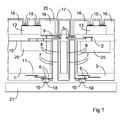
- Figure 1 is a cross section of an embodiment of the interposer-chip-arrangement.
- the interposer 1 which may be semiconductor material, especially a silicon wafer, for instance, has a main surface 10 and a further main surface 11 opposite the main surface.
- An integrated circuit 25 is arranged in the interposer 1 and is connected with at least one of the metal layers 5, which can be provided as a wiring of the integrated circuit 25.
- a further dielectric layer 3 is arranged above the further main surface 11 with at least one further metal layer 6 embedded in the further dielectric layer 3.
- An electrically conductive interconnection 7 through the interposer 1 connects one of the metal layers 5 and the further metal layer 6.
- the interconnection 7 can be formed by a metallization, which is arranged in a via hole and is preferably electrically insulated from the material of the interposer 1 by an insulation 8 at the sidewall of the via hole.
- the metallization of the interconnection 7 is applied on a contact area 9 of the relevant metal layer 5.
- the interconnection 7 can be formed as an open through-substrate via in the shape of a hollow cylinder surrounding an inner volume, which may be filled with dielectric material, for instance.
- a chip 12 comprising at least one contact pad 15 is arranged on or above the dielectric layer 2.
- the contact pad 15 is electrically conductively connected with the interconnection 7 by means of a structured metallization 20, which is applied on the contact pad 15 and on a metal layer 5 that is electrically conductively connected with the interconnection 7.
- bond wires may be applied to connect the contact pad 15 with the metal layer 5.
- a cover layer 16 may be applied on the dielectric layer 2 and on the chip 12. The cover layer 16 is provided with openings 17 above the contact pad 15 and above the metal layer 5 to enable the electrical connection.
- the further metal layer 6 can be provided as a redistribution layer or as part of a further wiring, for instance.
- a further contact area 19 on the further metal layer 6 can be provided with a bump contact 18, which can be a solder ball, for instance.
- the bump contact 18 serves as an external electrical connection, in particular as a connection with conductor tracks or the like when the interposer-chip-arrangement is mounted on a carrier like a printed circuit board 21, for instance.
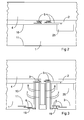
- Figure 2 is a cross section of the interposer 1 with the dielectric layer 2 and embedded metal layers 5 on its main surface 10.
- An integrated circuit 25 is connected to the metal layers 5, which serve as a wiring. Manufacture is facilitated if a handling wafer 4 is fastened to the upper surface of the dielectric layer 2.
- the interconnection 7 is produced from the further main surface 11 of the interposer 1, opposite the dielectric layer 2.
- Figure 3 is a cross section according to Figure 2 after the formation of the interconnection 7.
- the further dielectric layer 3 is arranged above the further main surface 11.
- the interconnection 7 can be produced by etching a via hole through the further dielectric layer 3 and the interposer 1, until a contact area 9 of one of the metal layers 5 is uncovered.
- a sidewall insulation 8 is preferably formed in the via hole, and a metallization is applied in the via hole, so that the metallization electrically contacts the contact area 9.
- the metallization yields the electrically conductive interconnection 7.
- At least one further metal layer 6, which is connected to the interconnection 7, is arranged in or on the further dielectric layer 3.
- the inner volume of the interconnection 7 can be filled with the material that is applied to form the further dielectric layer 3, which may be an oxide or nitride of semiconductor material, for instance.
- a further contact area 19 of the further metal layer 6 can be provided for an external electrical connection. The handling wafer 4 is then removed.
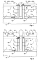
- Figure 4 is a cross section according to Figure 3 after the placement of chips. Manufacture is facilitated if a further handling wafer 14 is fastened to the further dielectric layer 3. A chip 12 and a further chip 13 are mounted on the dielectric layer 2. Any number of chips can thus be mounted above the main surface 10. Chips and integrated circuits 25 of the interposer 1 may especially be arranged in one-to-one correspondence to form a plurality of device units.
- Figure 5 is a cross section according to Figure 4 after the application of a planarizing cover layer 16, which may be a polymer, for instance, in particular a photosensitive organic polymer. Openings 17 are formed in the cover layer 16 above contact pads 15 of the chips 12, 13 and above the metal layers 5 in order to allow the contact pads 15 to be electrically connected with one of the metal layers 5 and thus with the interconnection 7.
- the electrical connection can be formed by an application of a structured metallization 20 as shown in Figure 1 or by an application of bond wires, which are known per se.
- a bump contact 18 can be applied on the further contact area 19, and the interposer-chip-arrangement according to Figure 1 is obtained.
- Figure 6 is a cross section according to Figure 3 after the formation of chip cavities for a further embodiment. Elements corresponding to similar elements of the embodiment according to Figure 3 are designated with the same reference numerals.
- a further handling wafer 14 is preferably fastened to the dielectric layer 3.
- Cavities 22, 23 are formed in the dielectric layer 2 and in the interposer 1.
- the cavities 22, 23, which are provided for the accomodation of chips, can be produced by etching and may have different depths. It may be suitable to arrange the cavities 22, 23 outside the region occupied by the integrated circuit 25, which is hence not shown in Figure 6 .
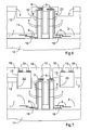
- FIG. 7 is a cross section according to Figure 6 after the placement of chips.
- a chip 12 is arranged in the cavity 22, and a further chip 13 is arranged in the further cavity 23.
- the chips 12, 13 have different sizes, and the depths of the cavities 22, 23 are different, so that the contact pads 15 of the chips 12, 13 are at the same level.
- the cavities 22, 23 can thus be adapted to the sizes of the chips 12, 13. Instead, the cavities 22, 23 can each have the same depth and the same lateral dimensions.
- the chips 12, 13 can be mounted in the cavities 22, 23 by means of an adhesive, for instance.
- the interposer 1 is a semiconductor material
- the chips 12, 13 can instead be fastened by a bonding process, which is known per se. If a bonding method is applied, the bottom of the cavity has to be sufficiently plain. This can be achieved by providing an etch stop layer in the interposer 1 at the position where the bottom of a cavity is to be formed.
- Figure 8 is a cross section according to Figure 7 after the application of a structured metallization 20, which connects areas of the contact pads 15 and the metal layers 5, which are uncovered in the openings 17 of the cover layer 16.
- a bump contact 18 may be applied on the further contact area 19 of the further metal layer 6 according to the embodiment shown in Figure 1 , and the interposer-chip-arrangement can be mounted on a printed circuit board 21.
- Figure 9 is a cross section according to Figure 6 for a further embodiment comprising cavities for the chips. Elements corresponding to similar elements of the embodiment according to Figure 6 are designated with the same reference numerals.
- the cavities 22, 23 are formed in the further dielectric layer 3 and in the further main surface 11 of the interposer 1.
- the cavities 22, 23 and the integrated circuits 25 are located on opposite sides of the interposer 1.
- the cavities 22, 23 can be produced by etching like the via hole that is provided for the interconnection 7.
- the further contact areas 19 of the further metal layer 6 are provided for a connection of the contact pads 15 of the chips 12, 13 with the corresponding interconnections 7.
- Figure 10 is a cross section according to Figure 9 after the placement of the chip 12 in the cavity 22 and the further chip 13 in the further cavity 23.
- the chips 12, 13 have different sizes, and the depths of the cavities 22, 23 are adapted so that the contact pads 15 of the chips 12, 13 are at the same level.
- the cavities 22, 23 can thus be adapted to the sizes of the chips 12, 13.
- the cavities 22, 23 can instead each have the same dimensions.
- the chips 12, 13 can be mounted in the cavities 22, 23 by means of an adhesive, for instance. If the interposer 1 is a semiconductor material, the chips 12, 13 can instead be fastened by a bonding process.
- a cover layer 16, which may be a polymer, may be applied on the further dielectric layer 3 and on the chip 12.
- the cover layer 16 is provided with openings 17 above the contact pads 15 and above the further contact areas 19 of the further metal layer 6.
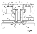
- Figure 11 is a cross section according to Figure 10 after the application of a structured metallization 20, which connects the contact pads 15 and the further contact areas 19 of the further metal layer 6 in the openings 17 of the cover layer 16.
- bump contacts 18 may be applied on the further contact areas 24 of the metal layers 5 according to the embodiment shown in Figure 8 , and the interposer-chip-arrangement can be mounted on a printed circuit board 21.
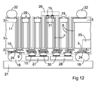
- Figure 12 is a cross section according to Figure 11 for a further embodiment comprising chips mounted in flip-chip technology. Elements corresponding to similar elements of the embodiment according to Figure 11 are designated with the same reference numerals.
- the interposer-chip-arrangement is provided with bump contacts 18 arranged on the further contact areas 24 above the main surface 10 of the interposer 1.
- the interposer-chip-arrangement is shown after it has been mounted on a printed circuit board 21 using the bump contacts 18.
- the contact areas 9 above the main surface 10 are connected by interconnections 7 with the further contact areas 19 above the further main surface 11.
- the further contact areas 19 can be provided with further bump contacts 32, which can be connected with contact pads of a further interposer or printed circuit board, for example.
- a chip 26 is arranged with its contact pads 15 connected to further contact areas 19 of the interposer 1 in order to connect the contact pads 15 electrically conductively with interconnections 7 of the interposer 1.
- the connections between the contact pads 15 and the corresponding further contact areas 19 can be provided by bump contacts 31 in flip-chip-technology.
- further chips 27, 28 can be arranged with their contact pads 15 connected to further contact areas 24 of the interposer 1. These connections can also be provided by bump contacts 30 in flip-chip-technology.
- the further chips 27, 28 are thus arranged between the interposer 1 and the printed circuit board 21. There may be any number of chips 26, 27, 28 mounted in this way by means of bump contacts 30, 31.
- An interconnection 7 can serve to connect bump contacts 18 and further bump contacts 32 of the interposer-chip-arrangement in order to provide an electrical connection through the interposer 1.
- An interconnection 7 can instead or additionally serve to connect a contact pad 15 of one of the mounted chips 12, 13, 26, 27, 28 with any further contact pad 15 of any of the mounted chips 12, 13, 26, 27, 28.
- the described interposer-chip-arrangement allows a reduction of the lateral and vertical dimensions of the chip package.
- Extremly flat and small wafer level packages are obtained by means of interconnections formed like through-substrate vias connecting redistribution metal layers on opposite sides of the interposer.
- the integrated circuit of the interposer yields an especially dense arrangement of the circuitry, additionally to the circuit components that are provided by the mounted chips.
Landscapes
- Production Of Multi-Layered Print Wiring Board (AREA)
- Physics & Mathematics (AREA)
- Geometry (AREA)
- Engineering & Computer Science (AREA)
- Manufacturing & Machinery (AREA)
Abstract
Description
- Dense packaging of semiconductor chips is achieved by techniques that allow a compact arrangement of chips in a housing, like wafer-to-wafer or chip-to-wafer direct bonding. Through-silicon vias (TSVs), which are also called through-substrate vias in more general applications, and advanced wiring methods can also be used to reduce the dimensions.
-
US 2007/0007641 A1 discloses a chip-embedded interposer structure comprising a silicon substrate with a cavity, an integrated circuit chip with a plurality of I/O pads arranged in the cavity, a plurality of through-substrate vias penetrating the substrate and rerouting conductors connected to the I/O pads and the through-substrate vias. -
US 2010/0171226 A1 discloses an IC with an array of TSVs, each TSV comprising an electrically conductive filler material surrounded by a dielectric liner. The TSVs are arranged in interior and exterior rows and columns. At least a portion of the TSVs are electrically connected to a terminating metal interconnect level. At least one of the exterior rows or columns includes a lower number of electrically connected TSVs than the interior rows and the interior columns. -
US 2011/0024916 A1 discloses a method of forming an interposer package with through-silicon vias. A semiconductor die and a dummy die provided with a through-silicon via are mounted over a carrier, the dies are encapsulated, and the carrier is removed. A first redistribution layer is formed over the dies, thus electrically connecting the through-silicon via and a contact pad of the semiconductor die. An insulation layer is formed over the first redistribution layer. A second redistribution layer is formed opposite the first redistribution layer and electrically connected to the through-silicon via. A semiconductor package is connected to the second redistribution layer. - M. Murugesan et al., "High-step-coverage Cu-lateral interconnections over 100 µm thick chips on a polymer substrate - an alternative method to wire bonding," in J. Micromech. Microeng. 22 (2012) 085033 doi:10.1088/0960-1317/22/8/085033, describe a method for packaging different kinds of chips on a wafer level. The resistance value of high-step-coverage interconnections formed by electroplating over 100 µm thick silicon chips was found to be very close to the resistance value of interconnections on the plain wafer even at 150°C. The method is suggested for the manufacture of CMOS compatible interconnections between a polymer substrate and a chip.
- Qianwen Chen et al., "Chip-to-Wafer (C2W) 3D Integration with Well-Controlled Template Alignment and Wafer-Level Bonding," in IEEE 61st Electronic Components and Technology Conference (ECTC 2011), describe the embedding of chips into cavities.
- Akitsu Shigetou and Tadatomo Suga, "Homo/Heterogeneous Bonding of Cu, SiO2, and Polyimide by Low Temperature Vapor-Assisted Surface Activation Method," in IEEE 61st Electronic Components and Technology Conference (ECTC 2011), describe polyimide bonding with thickness of 10 nm.
- It is an object of the present invention to disclose an interposer-chip-arrangement for dense packaging of chips and a method of producing the interposer-chip-arrangement.
- This object is achieved with the interposer-chip-arrangement according to
claim 1 and with the method of producing an interposer-chip-arrangement according toclaim 9. Embodiments derive from the dependent claims. - The interposer-chip-arrangement comprises an interposer having a main surface and a further main surface opposite the main surface, metal layers arranged above the main surface, a further metal layer arranged above the further main surface, an electrically conductive interconnection through the interposer, the interconnection connecting one of the metal layers and the further metal layer, a chip arranged at the main surface or at the further main surface, the chip having a contact pad, which is electrically conductively connected with the interconnection, a dielectric layer arranged above the main surface with the metal layers embedded in the dielectric layer, a further dielectric layer arranged above the further main surface with the further metal layer arranged in or on the further dielectric layer, and an integrated circuit in the interposer, the integrated circuit being connected with at least one of the metal layers.
- In an embodiment of the interposer-chip-arrangement, the contact pad of the chip is electrically conductively connected with the interconnection by a structured metallization.
- In a further embodiment, the contact pad of the chip is electrically conductively connected with the interconnection via one of the metal layers.
- In a further embodiment, the contact pad of the chip is electrically conductively connected with the interconnection via the further metal layer.
- In a further embodiment, the interconnection has the shape of a hollow cylinder and is filled with dielectric material.
- In a further embodiment, an insulation is arranged between the interposer and the interconnection.
- In a further embodiment, a cavity and a further cavity are formed in the main surface of the interposer or in the further main surface of the interposer, the cavities having different depths, the chip is arranged in the cavity, and a further chip is arranged in the further cavity.
- A method of producing the interposer-chip-arrangement comprises providing an interposer with an integrated circuit, arranging a dielectric layer with metal layers embedded in the dielectric layer above a main surface of the interposer, connecting the integrated circuit with at least one of the metal layers, forming an interconnection through the interposer, the interconnection contacting one of the metal layers, arranging a further dielectric layer above a further main surface of the interposer opposite the main surface with a further metal layer arranged in or on the further dielectric layer, the further metal layer being connected with the interconnection, arranging a chip provided with at least one contact pad at the main surface or at the further main surface, and electrically conductively connecting the contact pad with the interconnection.
- In a variant of the method, a structured metallization is applied to connect the contact pad with the interconnection.
- In further variants of the method, the contact pad is connected with the interconnection via one of the metal layers or via the further metal layer.
- In a further variant of the method, a cavity is formed in the interposer, and the chip is arranged in the cavity.
- In a further variant of the method, a further cavity is formed in the interposer, and a further chip provided with at least one contact pad is arranged in the further cavity, so that the contact pads of the chips are at the same level.
- In a further variant of the method, the interconnection is formed in the shape of a hollow cylinder and is filled with dielectric material.
- The following is a detailed description of embodiments of the interposer-chip-arrangement and of intermediate products of examples of the method.
- Figure 1
- is a cross section of an embodiment of the interposer-chip-arrangement.
- Figure 2
- is a cross section of an intermediate product of a method of producing the interposer-chip-arrangement.
- Figure 3
- is a cross section according to
Figure 2 after the formation of through-substrate-vias. - Figure 4
- is a cross section according to
Figure 3 after the placement of chips. - Figure 5
- is a cross section according to
Figure 4 after the application of a cover layer provided with openings. - Figure 6
- is a cross section according to
Figure 3 after the formation of chip cavities for a further embodiment. - Figure 7
- is a cross section according to
Figure 6 after the placement of chips. - Figure 8
- is a cross section according to
Figure 7 after the application of a metallization. - Figure 9
- is a cross section according to
Figure 6 for a further embodiment. - Figure 10
- is a cross section according to
Figure 9 after the placement of chips. - Figure 11
- is a cross section according to
Figure 10 after the application of a metallization. -
Figure 1 is a cross section of an embodiment of the interposer-chip-arrangement. Theinterposer 1, which may be semiconductor material, especially a silicon wafer, for instance, has amain surface 10 and a furthermain surface 11 opposite the main surface. Adielectric layer 2, which may be an oxide of the semiconductor material, for instance, is arranged above themain surface 10. Structured and interconnectedmetal layers 5 are embedded in thedielectric layer 2. An integratedcircuit 25 is arranged in theinterposer 1 and is connected with at least one of themetal layers 5, which can be provided as a wiring of the integratedcircuit 25. A furtherdielectric layer 3 is arranged above the furthermain surface 11 with at least onefurther metal layer 6 embedded in the furtherdielectric layer 3. - An electrically
conductive interconnection 7 through theinterposer 1 connects one of themetal layers 5 and thefurther metal layer 6. Theinterconnection 7 can be formed by a metallization, which is arranged in a via hole and is preferably electrically insulated from the material of theinterposer 1 by aninsulation 8 at the sidewall of the via hole. The metallization of theinterconnection 7 is applied on acontact area 9 of therelevant metal layer 5. Theinterconnection 7 can be formed as an open through-substrate via in the shape of a hollow cylinder surrounding an inner volume, which may be filled with dielectric material, for instance. - A
chip 12 comprising at least onecontact pad 15 is arranged on or above thedielectric layer 2. Thecontact pad 15 is electrically conductively connected with theinterconnection 7 by means of a structuredmetallization 20, which is applied on thecontact pad 15 and on ametal layer 5 that is electrically conductively connected with theinterconnection 7. Instead of the structuredmetallization 20, bond wires may be applied to connect thecontact pad 15 with themetal layer 5. Acover layer 16 may be applied on thedielectric layer 2 and on thechip 12. Thecover layer 16 is provided withopenings 17 above thecontact pad 15 and above themetal layer 5 to enable the electrical connection. - The
further metal layer 6 can be provided as a redistribution layer or as part of a further wiring, for instance. Afurther contact area 19 on thefurther metal layer 6 can be provided with abump contact 18, which can be a solder ball, for instance. Thebump contact 18 serves as an external electrical connection, in particular as a connection with conductor tracks or the like when the interposer-chip-arrangement is mounted on a carrier like a printedcircuit board 21, for instance. - A method for producing the interposer-chip-arrangement is described in the following in conjunction with
Figures 2 to 5 , which show cross sections of intermediate products. Elements corresponding to similar elements of the embodiment according toFigure 1 are designated with the same reference numerals. -
Figure 2 is a cross section of theinterposer 1 with thedielectric layer 2 and embeddedmetal layers 5 on itsmain surface 10. Anintegrated circuit 25 is connected to themetal layers 5, which serve as a wiring. Manufacture is facilitated if ahandling wafer 4 is fastened to the upper surface of thedielectric layer 2. Theinterconnection 7 is produced from the furthermain surface 11 of theinterposer 1, opposite thedielectric layer 2. -
Figure 3 is a cross section according toFigure 2 after the formation of theinterconnection 7. Thefurther dielectric layer 3 is arranged above the furthermain surface 11. Theinterconnection 7 can be produced by etching a via hole through thefurther dielectric layer 3 and theinterposer 1, until acontact area 9 of one of themetal layers 5 is uncovered. Asidewall insulation 8 is preferably formed in the via hole, and a metallization is applied in the via hole, so that the metallization electrically contacts thecontact area 9. The metallization yields the electricallyconductive interconnection 7. At least onefurther metal layer 6, which is connected to theinterconnection 7, is arranged in or on thefurther dielectric layer 3. The inner volume of theinterconnection 7 can be filled with the material that is applied to form thefurther dielectric layer 3, which may be an oxide or nitride of semiconductor material, for instance. Afurther contact area 19 of thefurther metal layer 6 can be provided for an external electrical connection. The handlingwafer 4 is then removed. -
Figure 4 is a cross section according toFigure 3 after the placement of chips. Manufacture is facilitated if afurther handling wafer 14 is fastened to thefurther dielectric layer 3. Achip 12 and afurther chip 13 are mounted on thedielectric layer 2. Any number of chips can thus be mounted above themain surface 10. Chips andintegrated circuits 25 of theinterposer 1 may especially be arranged in one-to-one correspondence to form a plurality of device units. -
Figure 5 is a cross section according toFigure 4 after the application of aplanarizing cover layer 16, which may be a polymer, for instance, in particular a photosensitive organic polymer.Openings 17 are formed in thecover layer 16 abovecontact pads 15 of thechips metal layers 5 in order to allow thecontact pads 15 to be electrically connected with one of themetal layers 5 and thus with theinterconnection 7. The electrical connection can be formed by an application of a structuredmetallization 20 as shown inFigure 1 or by an application of bond wires, which are known per se. After removal of thefurther handling wafer 14, abump contact 18 can be applied on thefurther contact area 19, and the interposer-chip-arrangement according toFigure 1 is obtained. -
Figure 6 is a cross section according toFigure 3 after the formation of chip cavities for a further embodiment. Elements corresponding to similar elements of the embodiment according toFigure 3 are designated with the same reference numerals. After the removal of thehandling wafer 4, afurther handling wafer 14 is preferably fastened to thedielectric layer 3.Cavities dielectric layer 2 and in theinterposer 1. Thecavities cavities circuit 25, which is hence not shown inFigure 6 . -
Figure 7 is a cross section according toFigure 6 after the placement of chips. Achip 12 is arranged in thecavity 22, and afurther chip 13 is arranged in thefurther cavity 23. In the embodiment shown inFigure 7 , thechips cavities contact pads 15 of thechips cavities chips cavities chips cavities interposer 1 is a semiconductor material, thechips interposer 1 at the position where the bottom of a cavity is to be formed. -
Figure 8 is a cross section according toFigure 7 after the application of a structuredmetallization 20, which connects areas of thecontact pads 15 and themetal layers 5, which are uncovered in theopenings 17 of thecover layer 16. After removal of thefurther handling wafer 14, abump contact 18 may be applied on thefurther contact area 19 of thefurther metal layer 6 according to the embodiment shown inFigure 1 , and the interposer-chip-arrangement can be mounted on a printedcircuit board 21. -
Figure 9 is a cross section according toFigure 6 for a further embodiment comprising cavities for the chips. Elements corresponding to similar elements of the embodiment according toFigure 6 are designated with the same reference numerals. In the embodiment according toFigure 9 , thecavities further dielectric layer 3 and in the furthermain surface 11 of theinterposer 1. Thecavities integrated circuits 25 are located on opposite sides of theinterposer 1. Thecavities interconnection 7. Thefurther contact areas 19 of thefurther metal layer 6 are provided for a connection of thecontact pads 15 of thechips corresponding interconnections 7. -
Figure 10 is a cross section according toFigure 9 after the placement of thechip 12 in thecavity 22 and thefurther chip 13 in thefurther cavity 23. In the embodiment shown inFigure 10 , thechips cavities contact pads 15 of thechips cavities chips cavities chips cavities interposer 1 is a semiconductor material, thechips cover layer 16, which may be a polymer, may be applied on thefurther dielectric layer 3 and on thechip 12. Thecover layer 16 is provided withopenings 17 above thecontact pads 15 and above thefurther contact areas 19 of thefurther metal layer 6. -
Figure 11 is a cross section according toFigure 10 after the application of a structuredmetallization 20, which connects thecontact pads 15 and thefurther contact areas 19 of thefurther metal layer 6 in theopenings 17 of thecover layer 16. After removal of thehandling wafer 4, bumpcontacts 18 may be applied on thefurther contact areas 24 of themetal layers 5 according to the embodiment shown inFigure 8 , and the interposer-chip-arrangement can be mounted on a printedcircuit board 21. -
Figure 12 is a cross section according toFigure 11 for a further embodiment comprising chips mounted in flip-chip technology. Elements corresponding to similar elements of the embodiment according toFigure 11 are designated with the same reference numerals. In the embodiment according toFigure 12 , the interposer-chip-arrangement is provided withbump contacts 18 arranged on thefurther contact areas 24 above themain surface 10 of theinterposer 1. InFigure 12 the interposer-chip-arrangement is shown after it has been mounted on a printedcircuit board 21 using thebump contacts 18. Thecontact areas 9 above themain surface 10 are connected byinterconnections 7 with thefurther contact areas 19 above the furthermain surface 11. Thefurther contact areas 19 can be provided withfurther bump contacts 32, which can be connected with contact pads of a further interposer or printed circuit board, for example. - Above the further
main surface 11, achip 26 is arranged with itscontact pads 15 connected tofurther contact areas 19 of theinterposer 1 in order to connect thecontact pads 15 electrically conductively withinterconnections 7 of theinterposer 1. The connections between thecontact pads 15 and the correspondingfurther contact areas 19 can be provided bybump contacts 31 in flip-chip-technology. Above themain surface 10, further chips 27, 28 can be arranged with theircontact pads 15 connected tofurther contact areas 24 of theinterposer 1. These connections can also be provided bybump contacts 30 in flip-chip-technology. Thefurther chips interposer 1 and the printedcircuit board 21. There may be any number ofchips bump contacts - An
interconnection 7 can serve to connectbump contacts 18 andfurther bump contacts 32 of the interposer-chip-arrangement in order to provide an electrical connection through theinterposer 1. Aninterconnection 7 can instead or additionally serve to connect acontact pad 15 of one of the mountedchips further contact pad 15 of any of the mountedchips - The described interposer-chip-arrangement allows a reduction of the lateral and vertical dimensions of the chip package. Extremly flat and small wafer level packages are obtained by means of interconnections formed like through-substrate vias connecting redistribution metal layers on opposite sides of the interposer. The integrated circuit of the interposer yields an especially dense arrangement of the circuitry, additionally to the circuit components that are provided by the mounted chips.
-
- 1
- interposer
- 2
- dielectric layer
- 3
- further dielectric layer
- 4
- handling wafer
- 5
- metal layer
- 6
- further metal layer
- 7
- interconnection
- 8
- sidewall insulation
- 9
- contact area
- 10
- main surface
- 11
- further main surface
- 12
- chip
- 13
- further chip
- 14
- further handling wafer
- 15
- contact pad
- 16
- cover layer
- 17
- opening
- 18
- bump contact
- 19
- further contact area
- 20
- metallization
- 21
- printed circuit board
- 22
- cavity
- 23
- further cavity
- 24
- further contact area
- 25
- integrated circuit
- 26
- chip
- 27
- further chip
- 28
- further chip
- 29
- passivation
- 30
- bump contact
- 31
- bump contact
- 32
- further bump contact
Claims (15)
- An interposer-chip-arrangement, comprising:- an interposer (1) with a main surface (10) and a further main surface (11) opposite the main surface (10),- metal layers (5) arranged above the main surface (10),- a further metal layer (6) arranged above the further main surface (11),- an electrically conductive interconnection (7) through the interposer (1), the interconnection (7) connecting one of the metal layers (5) and the further metal layer (6),- a chip (12) arranged at the main surface (10) or at the further main surface (11), and- a contact pad (15) of the chip (12), the contact pad (15) being electrically conductively connected with the interconnection (7),characterized in that- a dielectric layer (2) is arranged above the main surface (10) with the metal layers (5) embedded in the dielectric layer (2),- a further dielectric layer (3) is arranged above the further main surface (11) with the further metal layer (6) arranged in or on the further dielectric layer (3), and- the interposer (1) is provided with an integrated circuit (25), which is connected with at least one of the metal layers (5).
- The interposer-chip-arrangement of claim 1, wherein the contact pad (15) of the chip (12) is electrically conductively connected with the interconnection (7) by a structured metallization (20).
- The interposer-chip-arrangement of claim 1 or 2, wherein the contact pad (15) of the chip (12) is electrically conductively connected with the interconnection (7) via one of the metal layers (5).
- The interposer-chip-arrangement of claim 1 or 2, wherein the contact pad (15) of the chip (12) is electrically conductively connected with the interconnection (7) via the further metal layer (6).
- The interposer-chip-arrangement of one of claims 1 to 4, wherein the interconnection (7) has the shape of a hollow cylinder and is filled with dielectric material.
- The interposer-chip-arrangement of one of claims 1 to 5, further comprising:an insulation (8) arranged between the interposer (1) and the interconnection (7).
- The interposer-chip-arrangement of one of claims 1 to 6, further comprising:a cavity (22) in the main surface (10) of the interposer (1), the chip (12) being arranged in the cavity (22),a further chip (13), anda further cavity (23) in the main surface (10) of the interposer (1), the further chip (13) being arranged in the further cavity (23), and the cavities (22, 23) having different depths.
- The interposer-chip-arrangement of one of claims 1 to 6, further comprising:a cavity (22) in the further main surface (11) of the interposer (1), the chip (12) being arranged in the cavity (22),a further chip (13), anda further cavity (23) in the further main surface (11) of the interposer (1), the further chip (13) being arranged in the further cavity (23), and the cavities (22, 23) having different depths.
- A method of producing an interposer-chip-arrangement, comprising:- providing an interposer (1) with an integrated circuit (25),- arranging a dielectric layer (2) with metal layers (5) embedded in the dielectric layer (2) above a main surface (10) of the interposer (1),- connecting the integrated circuit (25) with at least one of the metal layers (5),- forming an interconnection (7) through the interposer (1), the interconnection (7) contacting one of the metal layers (5),- arranging a further dielectric layer (3) above a further main surface (11) of the interposer (1) opposite the main surface (10) and arranging a further metal layer (6) in or on the further dielectric layer (3), the further metal layer (6) being connected with the interconnection (7),- arranging a chip (12) provided with at least one contact pad (15) at the main surface (10) or at the further main surface (11), and- electrically conductively connecting the contact pad (15) with the interconnection (7).
- The method of claim 9, further comprising:applying a structured metallization (20) connecting the contact pad (15) with the interconnection (7).
- The method of claim 9 or 10, wherein the contact pad (15) is connected with the interconnection (7) via one of the metal layers (5).
- The method of claim 9 or 10, wherein the contact pad (15) is connected with the interconnection (7) via the further metal layer (6).
- The method of one of claims 9 to 12, further comprising:forming a cavity (22) in the interposer (1) and arranging the chip (12) in the cavity (22).
- The method of claim 13, further comprising:forming a further cavity (23) in the interposer (1) andarranging a further chip (13) provided with at least one contact pad (15) in the further cavity (23), so that the contact pads (15) of the chips (12, 13) are at the same level.
- The method of one of claims 9 to 14, wherein the interconnection (7) is formed in the shape of a hollow cylinder and is filled with dielectric material.
Priority Applications (2)
| Application Number | Priority Date | Filing Date | Title |
|---|---|---|---|
| US14/561,164 US9818724B2 (en) | 2013-12-05 | 2014-12-04 | Interposer-chip-arrangement for dense packaging of chips |
| US15/726,905 US10340254B2 (en) | 2013-12-05 | 2017-10-06 | Method of producing an interposer-chip-arrangement for dense packaging of chips |
Applications Claiming Priority (1)
| Application Number | Priority Date | Filing Date | Title |
|---|---|---|---|
| US201361912114P | 2013-12-05 | 2013-12-05 |
Publications (2)
| Publication Number | Publication Date |
|---|---|
| EP2881983A1 true EP2881983A1 (en) | 2015-06-10 |
| EP2881983B1 EP2881983B1 (en) | 2019-09-18 |
Family
ID=49880516
Family Applications (1)
| Application Number | Title | Priority Date | Filing Date |
|---|---|---|---|
| EP13198854.5A Active EP2881983B1 (en) | 2013-12-05 | 2013-12-20 | Interposer-chip-arrangement for dense packaging of chips |
Country Status (2)
| Country | Link |
|---|---|
| US (2) | US9818724B2 (en) |
| EP (1) | EP2881983B1 (en) |
Cited By (1)
| Publication number | Priority date | Publication date | Assignee | Title |
|---|---|---|---|---|
| CN112908984A (en) * | 2021-01-18 | 2021-06-04 | 上海先方半导体有限公司 | SSD (solid State disk) stacked packaging structure with radiating fins and manufacturing method thereof |
Families Citing this family (6)
| Publication number | Priority date | Publication date | Assignee | Title |
|---|---|---|---|---|
| US9543270B1 (en) * | 2015-07-31 | 2017-01-10 | Inotera Memories, Inc. | Multi-device package and manufacturing method thereof |
| US10986144B1 (en) * | 2015-09-28 | 2021-04-20 | HealthLinx Technologies, Inc. | System and method for collaboration over a network |
| US9960102B2 (en) * | 2016-06-13 | 2018-05-01 | Advanced Semiconductor Engineering, Inc. | Semiconductor devices and methods of manufacturing the same |
| CN112956019B (en) * | 2018-11-09 | 2023-06-02 | 华为技术有限公司 | Chip integrated with at least two bare chips |
| US11830842B2 (en) | 2020-10-22 | 2023-11-28 | NXP USA., Inc. | Hybrid device assemblies and method of fabrication |
| WO2025017397A1 (en) * | 2023-07-14 | 2025-01-23 | Medtronic, Inc. | Integrated circuit package and method of forming same |
Citations (5)
| Publication number | Priority date | Publication date | Assignee | Title |
|---|---|---|---|---|
| US20070007641A1 (en) | 2005-07-08 | 2007-01-11 | Kang-Wook Lee | Chip-embedded interposer structure and fabrication method thereof, wafer level stack structure and resultant package structure |
| US20100171226A1 (en) | 2008-12-29 | 2010-07-08 | Texas Instruments, Inc. | Ic having tsv arrays with reduced tsv induced stress |
| US20110024916A1 (en) | 2008-12-01 | 2011-02-03 | Stats Chippac, Ltd. | Semiconductor Device and Method of Forming an Interposer Package with Through Silicon Vias |
| US20110024887A1 (en) * | 2009-07-31 | 2011-02-03 | Chi Heejo | Integrated circuit packaging system with through silicon via base and method of manufacture thereof |
| WO2011097089A2 (en) * | 2010-02-03 | 2011-08-11 | Marvell World Trade Ltd. | Recessed semiconductor substrates |
Family Cites Families (29)
| Publication number | Priority date | Publication date | Assignee | Title |
|---|---|---|---|---|
| DE3633181C2 (en) | 1986-09-30 | 1998-12-10 | Siemens Ag | Reflex light barrier |
| JP2985691B2 (en) | 1994-03-23 | 1999-12-06 | 株式会社デンソー | Semiconductor device |
| DE19859669A1 (en) | 1998-12-23 | 2000-06-29 | Heidenhain Gmbh Dr Johannes | Integrated optoelectronic sensor and method for its production |
| JP2001024150A (en) * | 1999-07-06 | 2001-01-26 | Sony Corp | Semiconductor device |
| JP4711029B2 (en) | 2000-12-04 | 2011-06-29 | 住友電気工業株式会社 | Optical communication device |
| DE10309747B4 (en) | 2002-03-07 | 2011-11-24 | CiS Institut für Mikrosensorik gGmbH | Auflichtsensor and method for its preparation |
| DE10352741B4 (en) | 2003-11-12 | 2012-08-16 | Austriamicrosystems Ag | Radiation-detecting optoelectronic component, process for its production and use |
| JP4252019B2 (en) * | 2004-09-01 | 2009-04-08 | 三洋電機株式会社 | Circuit device and manufacturing method thereof |
| JP4061409B2 (en) | 2004-11-09 | 2008-03-19 | 国立大学法人九州大学 | Sensor unit and biosensor |
| JP2006203111A (en) | 2005-01-24 | 2006-08-03 | Hosiden Corp | Object detection sensor |
| JP2007027621A (en) | 2005-07-21 | 2007-02-01 | Rohm Co Ltd | Surface mount type photo interrupter and manufacturing method thereof |
| JP2007199328A (en) | 2006-01-26 | 2007-08-09 | Fuji Xerox Co Ltd | Optical coupling device |
| JP2010034189A (en) | 2008-07-28 | 2010-02-12 | Sharp Corp | Optical proximity sensor, method of manufacturing the same, and electronic apparatus mounted with the same |
| JP4871344B2 (en) | 2008-11-25 | 2012-02-08 | 株式会社東芝 | Light emitting device and manufacturing method thereof |
| US8212202B2 (en) | 2009-01-08 | 2012-07-03 | Avago Technologies Ecbu Ip (Singapore) Pte. Ltd. | Reflective optical encoder package and method |
| US8324602B2 (en) | 2009-04-14 | 2012-12-04 | Intersil Americas Inc. | Optical sensors that reduce specular reflections |
| US8779361B2 (en) | 2009-06-30 | 2014-07-15 | Avago Technologies General Ip (Singapore) Pte. Ltd. | Optical proximity sensor package with molded infrared light rejection barrier and infrared pass components |
| US20110089531A1 (en) * | 2009-10-16 | 2011-04-21 | Teledyne Scientific & Imaging, Llc | Interposer Based Monolithic Microwave Integrate Circuit (iMMIC) |
| US8492720B2 (en) | 2010-06-08 | 2013-07-23 | Avago Technologies General Ip (Singapore) Pte. Ltd. | Small low-profile optical proximity sensor |
| US8518746B2 (en) | 2010-09-02 | 2013-08-27 | Stats Chippac, Ltd. | Semiconductor device and method of forming TSV semiconductor wafer with embedded semiconductor die |
| US8928159B2 (en) * | 2010-09-02 | 2015-01-06 | Taiwan Semiconductor Manufacturing & Company, Ltd. | Alignment marks in substrate having through-substrate via (TSV) |
| TWI434387B (en) * | 2010-10-11 | 2014-04-11 | 日月光半導體製造股份有限公司 | Semiconductor device having via hole and package structure of semiconductor device having via hole and manufacturing method thereof |
| US9398694B2 (en) * | 2011-01-18 | 2016-07-19 | Sony Corporation | Method of manufacturing a package for embedding one or more electronic components |
| FR2973573A1 (en) | 2011-04-01 | 2012-10-05 | St Microelectronics Grenoble 2 | SEMICONDUCTOR HOUSING COMPRISING AN OPTICAL SEMICONDUCTOR DEVICE |
| JP5399525B2 (en) | 2011-06-29 | 2014-01-29 | シャープ株式会社 | Optical distance measuring device and electronic device |
| FR2977714B1 (en) | 2011-07-08 | 2013-07-26 | St Microelectronics Grenoble 2 | OPTICAL ELECTRONIC HOUSING |
| US9385058B1 (en) * | 2012-12-29 | 2016-07-05 | Monolithic 3D Inc. | Semiconductor device and structure |
| US8912663B1 (en) * | 2013-06-28 | 2014-12-16 | Delta Electronics, Inc. | Embedded package structure and method for manufacturing thereof |
| US9525094B2 (en) | 2015-03-27 | 2016-12-20 | Stmicroelectronics (Grenoble 2) Sas | Proximity and ranging sensor |
-
2013
- 2013-12-20 EP EP13198854.5A patent/EP2881983B1/en active Active
-
2014
- 2014-12-04 US US14/561,164 patent/US9818724B2/en active Active
-
2017
- 2017-10-06 US US15/726,905 patent/US10340254B2/en active Active
Patent Citations (5)
| Publication number | Priority date | Publication date | Assignee | Title |
|---|---|---|---|---|
| US20070007641A1 (en) | 2005-07-08 | 2007-01-11 | Kang-Wook Lee | Chip-embedded interposer structure and fabrication method thereof, wafer level stack structure and resultant package structure |
| US20110024916A1 (en) | 2008-12-01 | 2011-02-03 | Stats Chippac, Ltd. | Semiconductor Device and Method of Forming an Interposer Package with Through Silicon Vias |
| US20100171226A1 (en) | 2008-12-29 | 2010-07-08 | Texas Instruments, Inc. | Ic having tsv arrays with reduced tsv induced stress |
| US20110024887A1 (en) * | 2009-07-31 | 2011-02-03 | Chi Heejo | Integrated circuit packaging system with through silicon via base and method of manufacture thereof |
| WO2011097089A2 (en) * | 2010-02-03 | 2011-08-11 | Marvell World Trade Ltd. | Recessed semiconductor substrates |
Non-Patent Citations (4)
Cited By (1)
| Publication number | Priority date | Publication date | Assignee | Title |
|---|---|---|---|---|
| CN112908984A (en) * | 2021-01-18 | 2021-06-04 | 上海先方半导体有限公司 | SSD (solid State disk) stacked packaging structure with radiating fins and manufacturing method thereof |
Also Published As
| Publication number | Publication date |
|---|---|
| US9818724B2 (en) | 2017-11-14 |
| US20180096969A1 (en) | 2018-04-05 |
| US10340254B2 (en) | 2019-07-02 |
| EP2881983B1 (en) | 2019-09-18 |
| US20150162308A1 (en) | 2015-06-11 |
Similar Documents
| Publication | Publication Date | Title |
|---|---|---|
| US12261151B2 (en) | Integrated circuit packages | |
| US10777502B2 (en) | Semiconductor chip, package structure, and pacakge-on-package structure | |
| US10340254B2 (en) | Method of producing an interposer-chip-arrangement for dense packaging of chips | |
| TWI467734B (en) | Semiconductor component | |
| US9741696B2 (en) | Thermal vias disposed in a substrate proximate to a well thereof | |
| EP2351077B1 (en) | Through-substrate via and redistribution layer with metal paste | |
| KR102296721B1 (en) | Thermal vias disposed in a substrate without a liner layer | |
| CN104882417B (en) | Integrating passive Flip-Chip Using | |
| US20090212420A1 (en) | integrated circuit device and method for fabricating same | |
| US9190347B2 (en) | Die edge contacts for semiconductor devices | |
| TW202025439A (en) | Wafer-level stack chip package and method of manufacturing the same | |
| CN110085523A (en) | Semiconductor devices and its manufacturing method | |
| US12027455B2 (en) | Chip-on-wafer structure with Chiplet Interposer | |
| KR102469446B1 (en) | Semiconductor structure and method forming same | |
| US20240047404A1 (en) | Semiconductor structure | |
| US20230352418A1 (en) | Semiconductor die, semiconductor package and manufacturing method thereof | |
| US20260090367A1 (en) | Semiconductor die, semiconductor package and manufacturing method of semiconductor die | |
| KR20090131733A (en) | Semiconductor Package Manufacturing Method |
Legal Events
| Date | Code | Title | Description |
|---|---|---|---|
| PUAI | Public reference made under article 153(3) epc to a published international application that has entered the european phase |
Free format text: ORIGINAL CODE: 0009012 |
|
| 17P | Request for examination filed |
Effective date: 20131220 |
|
| AK | Designated contracting states |
Kind code of ref document: A1 Designated state(s): AL AT BE BG CH CY CZ DE DK EE ES FI FR GB GR HR HU IE IS IT LI LT LU LV MC MK MT NL NO PL PT RO RS SE SI SK SM TR |
|
| AX | Request for extension of the european patent |
Extension state: BA ME |
|
| R17P | Request for examination filed (corrected) |
Effective date: 20151116 |
|
| RBV | Designated contracting states (corrected) |
Designated state(s): AL AT BE BG CH CY CZ DE DK EE ES FI FR GB GR HR HU IE IS IT LI LT LU LV MC MK MT NL NO PL PT RO RS SE SI SK SM TR |
|
| STAA | Information on the status of an ep patent application or granted ep patent |
Free format text: STATUS: EXAMINATION IS IN PROGRESS |
|
| 17Q | First examination report despatched |
Effective date: 20181113 |
|
| RAP1 | Party data changed (applicant data changed or rights of an application transferred) |
Owner name: AMS AG |
|
| REG | Reference to a national code |
Ref country code: DE Ref legal event code: R079 Ref document number: 602013060633 Country of ref document: DE Free format text: PREVIOUS MAIN CLASS: H01L0023000000 Ipc: H01L0021600000 |
|
| GRAP | Despatch of communication of intention to grant a patent |
Free format text: ORIGINAL CODE: EPIDOSNIGR1 |
|
| STAA | Information on the status of an ep patent application or granted ep patent |
Free format text: STATUS: GRANT OF PATENT IS INTENDED |
|
| RIC1 | Information provided on ipc code assigned before grant |
Ipc: H01L 25/065 20060101ALI20190315BHEP Ipc: H01L 21/683 20060101ALN20190315BHEP Ipc: H01L 21/60 20060101AFI20190315BHEP |
|
| INTG | Intention to grant announced |
Effective date: 20190410 |
|
| GRAS | Grant fee paid |
Free format text: ORIGINAL CODE: EPIDOSNIGR3 |
|
| GRAA | (expected) grant |
Free format text: ORIGINAL CODE: 0009210 |
|
| STAA | Information on the status of an ep patent application or granted ep patent |
Free format text: STATUS: THE PATENT HAS BEEN GRANTED |
|
| RIN1 | Information on inventor provided before grant (corrected) |
Inventor name: SCHRANK, FRANZ Inventor name: KRAFT, JOCHEN Inventor name: SCHREMS, MARTIN |
|
| AK | Designated contracting states |
Kind code of ref document: B1 Designated state(s): AL AT BE BG CH CY CZ DE DK EE ES FI FR GB GR HR HU IE IS IT LI LT LU LV MC MK MT NL NO PL PT RO RS SE SI SK SM TR |
|
| REG | Reference to a national code |
Ref country code: GB Ref legal event code: FG4D |
|
| REG | Reference to a national code |
Ref country code: CH Ref legal event code: EP |
|
| REG | Reference to a national code |
Ref country code: DE Ref legal event code: R096 Ref document number: 602013060633 Country of ref document: DE |
|
| REG | Reference to a national code |
Ref country code: AT Ref legal event code: REF Ref document number: 1182305 Country of ref document: AT Kind code of ref document: T Effective date: 20191015 |
|
| REG | Reference to a national code |
Ref country code: IE Ref legal event code: FG4D |
|
| REG | Reference to a national code |
Ref country code: NL Ref legal event code: MP Effective date: 20190918 |
|
| PG25 | Lapsed in a contracting state [announced via postgrant information from national office to epo] |
Ref country code: FI Free format text: LAPSE BECAUSE OF FAILURE TO SUBMIT A TRANSLATION OF THE DESCRIPTION OR TO PAY THE FEE WITHIN THE PRESCRIBED TIME-LIMIT Effective date: 20190918 Ref country code: LT Free format text: LAPSE BECAUSE OF FAILURE TO SUBMIT A TRANSLATION OF THE DESCRIPTION OR TO PAY THE FEE WITHIN THE PRESCRIBED TIME-LIMIT Effective date: 20190918 Ref country code: HR Free format text: LAPSE BECAUSE OF FAILURE TO SUBMIT A TRANSLATION OF THE DESCRIPTION OR TO PAY THE FEE WITHIN THE PRESCRIBED TIME-LIMIT Effective date: 20190918 Ref country code: NO Free format text: LAPSE BECAUSE OF FAILURE TO SUBMIT A TRANSLATION OF THE DESCRIPTION OR TO PAY THE FEE WITHIN THE PRESCRIBED TIME-LIMIT Effective date: 20191218 Ref country code: SE Free format text: LAPSE BECAUSE OF FAILURE TO SUBMIT A TRANSLATION OF THE DESCRIPTION OR TO PAY THE FEE WITHIN THE PRESCRIBED TIME-LIMIT Effective date: 20190918 Ref country code: BG Free format text: LAPSE BECAUSE OF FAILURE TO SUBMIT A TRANSLATION OF THE DESCRIPTION OR TO PAY THE FEE WITHIN THE PRESCRIBED TIME-LIMIT Effective date: 20191218 |
|
| REG | Reference to a national code |
Ref country code: LT Ref legal event code: MG4D |
|
| PG25 | Lapsed in a contracting state [announced via postgrant information from national office to epo] |
Ref country code: GR Free format text: LAPSE BECAUSE OF FAILURE TO SUBMIT A TRANSLATION OF THE DESCRIPTION OR TO PAY THE FEE WITHIN THE PRESCRIBED TIME-LIMIT Effective date: 20191219 Ref country code: AL Free format text: LAPSE BECAUSE OF FAILURE TO SUBMIT A TRANSLATION OF THE DESCRIPTION OR TO PAY THE FEE WITHIN THE PRESCRIBED TIME-LIMIT Effective date: 20190918 Ref country code: LV Free format text: LAPSE BECAUSE OF FAILURE TO SUBMIT A TRANSLATION OF THE DESCRIPTION OR TO PAY THE FEE WITHIN THE PRESCRIBED TIME-LIMIT Effective date: 20190918 Ref country code: RS Free format text: LAPSE BECAUSE OF FAILURE TO SUBMIT A TRANSLATION OF THE DESCRIPTION OR TO PAY THE FEE WITHIN THE PRESCRIBED TIME-LIMIT Effective date: 20190918 |
|
| REG | Reference to a national code |
Ref country code: AT Ref legal event code: MK05 Ref document number: 1182305 Country of ref document: AT Kind code of ref document: T Effective date: 20190918 |
|
| PG25 | Lapsed in a contracting state [announced via postgrant information from national office to epo] |
Ref country code: PL Free format text: LAPSE BECAUSE OF FAILURE TO SUBMIT A TRANSLATION OF THE DESCRIPTION OR TO PAY THE FEE WITHIN THE PRESCRIBED TIME-LIMIT Effective date: 20190918 Ref country code: EE Free format text: LAPSE BECAUSE OF FAILURE TO SUBMIT A TRANSLATION OF THE DESCRIPTION OR TO PAY THE FEE WITHIN THE PRESCRIBED TIME-LIMIT Effective date: 20190918 Ref country code: IT Free format text: LAPSE BECAUSE OF FAILURE TO SUBMIT A TRANSLATION OF THE DESCRIPTION OR TO PAY THE FEE WITHIN THE PRESCRIBED TIME-LIMIT Effective date: 20190918 Ref country code: NL Free format text: LAPSE BECAUSE OF FAILURE TO SUBMIT A TRANSLATION OF THE DESCRIPTION OR TO PAY THE FEE WITHIN THE PRESCRIBED TIME-LIMIT Effective date: 20190918 Ref country code: AT Free format text: LAPSE BECAUSE OF FAILURE TO SUBMIT A TRANSLATION OF THE DESCRIPTION OR TO PAY THE FEE WITHIN THE PRESCRIBED TIME-LIMIT Effective date: 20190918 Ref country code: RO Free format text: LAPSE BECAUSE OF FAILURE TO SUBMIT A TRANSLATION OF THE DESCRIPTION OR TO PAY THE FEE WITHIN THE PRESCRIBED TIME-LIMIT Effective date: 20190918 Ref country code: ES Free format text: LAPSE BECAUSE OF FAILURE TO SUBMIT A TRANSLATION OF THE DESCRIPTION OR TO PAY THE FEE WITHIN THE PRESCRIBED TIME-LIMIT Effective date: 20190918 Ref country code: PT Free format text: LAPSE BECAUSE OF FAILURE TO SUBMIT A TRANSLATION OF THE DESCRIPTION OR TO PAY THE FEE WITHIN THE PRESCRIBED TIME-LIMIT Effective date: 20200120 |
|
| PG25 | Lapsed in a contracting state [announced via postgrant information from national office to epo] |
Ref country code: SK Free format text: LAPSE BECAUSE OF FAILURE TO SUBMIT A TRANSLATION OF THE DESCRIPTION OR TO PAY THE FEE WITHIN THE PRESCRIBED TIME-LIMIT Effective date: 20190918 Ref country code: SM Free format text: LAPSE BECAUSE OF FAILURE TO SUBMIT A TRANSLATION OF THE DESCRIPTION OR TO PAY THE FEE WITHIN THE PRESCRIBED TIME-LIMIT Effective date: 20190918 Ref country code: IS Free format text: LAPSE BECAUSE OF FAILURE TO SUBMIT A TRANSLATION OF THE DESCRIPTION OR TO PAY THE FEE WITHIN THE PRESCRIBED TIME-LIMIT Effective date: 20200224 Ref country code: CZ Free format text: LAPSE BECAUSE OF FAILURE TO SUBMIT A TRANSLATION OF THE DESCRIPTION OR TO PAY THE FEE WITHIN THE PRESCRIBED TIME-LIMIT Effective date: 20190918 |
|
| REG | Reference to a national code |
Ref country code: DE Ref legal event code: R097 Ref document number: 602013060633 Country of ref document: DE |
|
| PLBE | No opposition filed within time limit |
Free format text: ORIGINAL CODE: 0009261 |
|
| STAA | Information on the status of an ep patent application or granted ep patent |
Free format text: STATUS: NO OPPOSITION FILED WITHIN TIME LIMIT |
|
| PG2D | Information on lapse in contracting state deleted |
Ref country code: IS |
|
| PG25 | Lapsed in a contracting state [announced via postgrant information from national office to epo] |
Ref country code: DK Free format text: LAPSE BECAUSE OF FAILURE TO SUBMIT A TRANSLATION OF THE DESCRIPTION OR TO PAY THE FEE WITHIN THE PRESCRIBED TIME-LIMIT Effective date: 20190918 Ref country code: IS Free format text: LAPSE BECAUSE OF FAILURE TO SUBMIT A TRANSLATION OF THE DESCRIPTION OR TO PAY THE FEE WITHIN THE PRESCRIBED TIME-LIMIT Effective date: 20200119 |
|
| REG | Reference to a national code |
Ref country code: CH Ref legal event code: PL |
|
| 26N | No opposition filed |
Effective date: 20200619 |
|
| REG | Reference to a national code |
Ref country code: BE Ref legal event code: MM Effective date: 20191231 |
|
| PG25 | Lapsed in a contracting state [announced via postgrant information from national office to epo] |
Ref country code: SI Free format text: LAPSE BECAUSE OF FAILURE TO SUBMIT A TRANSLATION OF THE DESCRIPTION OR TO PAY THE FEE WITHIN THE PRESCRIBED TIME-LIMIT Effective date: 20190918 Ref country code: MC Free format text: LAPSE BECAUSE OF FAILURE TO SUBMIT A TRANSLATION OF THE DESCRIPTION OR TO PAY THE FEE WITHIN THE PRESCRIBED TIME-LIMIT Effective date: 20190918 |
|
| PG25 | Lapsed in a contracting state [announced via postgrant information from national office to epo] |
Ref country code: LU Free format text: LAPSE BECAUSE OF NON-PAYMENT OF DUE FEES Effective date: 20191220 Ref country code: IE Free format text: LAPSE BECAUSE OF NON-PAYMENT OF DUE FEES Effective date: 20191220 |
|
| PG25 | Lapsed in a contracting state [announced via postgrant information from national office to epo] |
Ref country code: BE Free format text: LAPSE BECAUSE OF NON-PAYMENT OF DUE FEES Effective date: 20191231 Ref country code: LI Free format text: LAPSE BECAUSE OF NON-PAYMENT OF DUE FEES Effective date: 20191231 Ref country code: CH Free format text: LAPSE BECAUSE OF NON-PAYMENT OF DUE FEES Effective date: 20191231 |
|
| PG25 | Lapsed in a contracting state [announced via postgrant information from national office to epo] |
Ref country code: CY Free format text: LAPSE BECAUSE OF FAILURE TO SUBMIT A TRANSLATION OF THE DESCRIPTION OR TO PAY THE FEE WITHIN THE PRESCRIBED TIME-LIMIT Effective date: 20190918 |
|
| PG25 | Lapsed in a contracting state [announced via postgrant information from national office to epo] |
Ref country code: HU Free format text: LAPSE BECAUSE OF FAILURE TO SUBMIT A TRANSLATION OF THE DESCRIPTION OR TO PAY THE FEE WITHIN THE PRESCRIBED TIME-LIMIT; INVALID AB INITIO Effective date: 20131220 Ref country code: MT Free format text: LAPSE BECAUSE OF FAILURE TO SUBMIT A TRANSLATION OF THE DESCRIPTION OR TO PAY THE FEE WITHIN THE PRESCRIBED TIME-LIMIT Effective date: 20190918 |
|
| PG25 | Lapsed in a contracting state [announced via postgrant information from national office to epo] |
Ref country code: TR Free format text: LAPSE BECAUSE OF FAILURE TO SUBMIT A TRANSLATION OF THE DESCRIPTION OR TO PAY THE FEE WITHIN THE PRESCRIBED TIME-LIMIT Effective date: 20190918 |
|
| PG25 | Lapsed in a contracting state [announced via postgrant information from national office to epo] |
Ref country code: MK Free format text: LAPSE BECAUSE OF FAILURE TO SUBMIT A TRANSLATION OF THE DESCRIPTION OR TO PAY THE FEE WITHIN THE PRESCRIBED TIME-LIMIT Effective date: 20190918 |
|
| P01 | Opt-out of the competence of the unified patent court (upc) registered |
Effective date: 20230822 |
|
| REG | Reference to a national code |
Ref country code: DE Ref legal event code: R079 Ref document number: 602013060633 Country of ref document: DE Free format text: PREVIOUS MAIN CLASS: H01L0021600000 Ipc: H10W0070010000 |
|
| PGFP | Annual fee paid to national office [announced via postgrant information from national office to epo] |
Ref country code: DE Payment date: 20251211 Year of fee payment: 13 |
|
| PGFP | Annual fee paid to national office [announced via postgrant information from national office to epo] |
Ref country code: GB Payment date: 20251219 Year of fee payment: 13 |
|
| PGFP | Annual fee paid to national office [announced via postgrant information from national office to epo] |
Ref country code: FR Payment date: 20251223 Year of fee payment: 13 |