EP2881761A1 - Composite sensor and composite sensor module - Google Patents
Composite sensor and composite sensor module Download PDFInfo
- Publication number
- EP2881761A1 EP2881761A1 EP13825122.8A EP13825122A EP2881761A1 EP 2881761 A1 EP2881761 A1 EP 2881761A1 EP 13825122 A EP13825122 A EP 13825122A EP 2881761 A1 EP2881761 A1 EP 2881761A1
- Authority
- EP
- European Patent Office
- Prior art keywords
- substrate
- thermal image
- image sensor
- image sensors
- composite sensor
- Prior art date
- Legal status (The legal status is an assumption and is not a legal conclusion. Google has not performed a legal analysis and makes no representation as to the accuracy of the status listed.)
- Granted
Links
Images



Classifications
-
- G—PHYSICS
- G01—MEASURING; TESTING
- G01J—MEASUREMENT OF INTENSITY, VELOCITY, SPECTRAL CONTENT, POLARISATION, PHASE OR PULSE CHARACTERISTICS OF INFRARED, VISIBLE OR ULTRAVIOLET LIGHT; COLORIMETRY; RADIATION PYROMETRY
- G01J5/00—Radiation pyrometry, e.g. infrared or optical thermometry
- G01J5/10—Radiation pyrometry, e.g. infrared or optical thermometry using electric radiation detectors
- G01J5/12—Radiation pyrometry, e.g. infrared or optical thermometry using electric radiation detectors using thermoelectric elements, e.g. thermocouples
-
- G—PHYSICS
- G01—MEASURING; TESTING
- G01C—MEASURING DISTANCES, LEVELS OR BEARINGS; SURVEYING; NAVIGATION; GYROSCOPIC INSTRUMENTS; PHOTOGRAMMETRY OR VIDEOGRAMMETRY
- G01C3/00—Measuring distances in line of sight; Optical rangefinders
- G01C3/02—Details
-
- G—PHYSICS
- G01—MEASURING; TESTING
- G01J—MEASUREMENT OF INTENSITY, VELOCITY, SPECTRAL CONTENT, POLARISATION, PHASE OR PULSE CHARACTERISTICS OF INFRARED, VISIBLE OR ULTRAVIOLET LIGHT; COLORIMETRY; RADIATION PYROMETRY
- G01J1/00—Photometry, e.g. photographic exposure meter
- G01J1/02—Details
- G01J1/04—Optical or mechanical part supplementary adjustable parts
- G01J1/0407—Optical elements not provided otherwise, e.g. manifolds, windows, holograms, gratings
-
- G—PHYSICS
- G01—MEASURING; TESTING
- G01J—MEASUREMENT OF INTENSITY, VELOCITY, SPECTRAL CONTENT, POLARISATION, PHASE OR PULSE CHARACTERISTICS OF INFRARED, VISIBLE OR ULTRAVIOLET LIGHT; COLORIMETRY; RADIATION PYROMETRY
- G01J3/00—Spectrometry; Spectrophotometry; Monochromators; Measuring colours
- G01J3/28—Investigating the spectrum
- G01J3/30—Measuring the intensity of spectral lines directly on the spectrum itself
- G01J3/36—Investigating two or more bands of a spectrum by separate detectors
-
- G—PHYSICS
- G01—MEASURING; TESTING
- G01J—MEASUREMENT OF INTENSITY, VELOCITY, SPECTRAL CONTENT, POLARISATION, PHASE OR PULSE CHARACTERISTICS OF INFRARED, VISIBLE OR ULTRAVIOLET LIGHT; COLORIMETRY; RADIATION PYROMETRY
- G01J5/00—Radiation pyrometry, e.g. infrared or optical thermometry
- G01J5/02—Constructional details
- G01J5/0275—Control or determination of height or distance or angle information for sensors or receivers
-
- G—PHYSICS
- G01—MEASURING; TESTING
- G01J—MEASUREMENT OF INTENSITY, VELOCITY, SPECTRAL CONTENT, POLARISATION, PHASE OR PULSE CHARACTERISTICS OF INFRARED, VISIBLE OR ULTRAVIOLET LIGHT; COLORIMETRY; RADIATION PYROMETRY
- G01J5/00—Radiation pyrometry, e.g. infrared or optical thermometry
- G01J5/02—Constructional details
- G01J5/04—Casings
- G01J5/041—Mountings in enclosures or in a particular environment
- G01J5/045—Sealings; Vacuum enclosures; Encapsulated packages; Wafer bonding structures; Getter arrangements
-
- G—PHYSICS
- G01—MEASURING; TESTING
- G01J—MEASUREMENT OF INTENSITY, VELOCITY, SPECTRAL CONTENT, POLARISATION, PHASE OR PULSE CHARACTERISTICS OF INFRARED, VISIBLE OR ULTRAVIOLET LIGHT; COLORIMETRY; RADIATION PYROMETRY
- G01J5/00—Radiation pyrometry, e.g. infrared or optical thermometry
- G01J5/02—Constructional details
- G01J5/08—Optical arrangements
- G01J5/0859—Sighting arrangements, e.g. cameras
-
- G—PHYSICS
- G01—MEASURING; TESTING
- G01S—RADIO DIRECTION-FINDING; RADIO NAVIGATION; DETERMINING DISTANCE OR VELOCITY BY USE OF RADIO WAVES; LOCATING OR PRESENCE-DETECTING BY USE OF THE REFLECTION OR RERADIATION OF RADIO WAVES; ANALOGOUS ARRANGEMENTS USING OTHER WAVES
- G01S17/00—Systems using the reflection or reradiation of electromagnetic waves other than radio waves, e.g. lidar systems
- G01S17/86—Combinations of lidar systems with systems other than lidar, radar or sonar, e.g. with direction finders
-
- G—PHYSICS
- G01—MEASURING; TESTING
- G01S—RADIO DIRECTION-FINDING; RADIO NAVIGATION; DETERMINING DISTANCE OR VELOCITY BY USE OF RADIO WAVES; LOCATING OR PRESENCE-DETECTING BY USE OF THE REFLECTION OR RERADIATION OF RADIO WAVES; ANALOGOUS ARRANGEMENTS USING OTHER WAVES
- G01S7/00—Details of systems according to groups G01S13/00, G01S15/00, G01S17/00
- G01S7/48—Details of systems according to groups G01S13/00, G01S15/00, G01S17/00 of systems according to group G01S17/00
- G01S7/481—Constructional features, e.g. arrangements of optical elements
- G01S7/4816—Constructional features, e.g. arrangements of optical elements of receivers alone
-
- H—ELECTRICITY
- H04—ELECTRIC COMMUNICATION TECHNIQUE
- H04N—PICTORIAL COMMUNICATION, e.g. TELEVISION
- H04N23/00—Cameras or camera modules comprising electronic image sensors; Control thereof
- H04N23/20—Cameras or camera modules comprising electronic image sensors; Control thereof for generating image signals from infrared radiation only
- H04N23/23—Cameras or camera modules comprising electronic image sensors; Control thereof for generating image signals from infrared radiation only from thermal infrared radiation
-
- H—ELECTRICITY
- H04—ELECTRIC COMMUNICATION TECHNIQUE
- H04N—PICTORIAL COMMUNICATION, e.g. TELEVISION
- H04N25/00—Circuitry of solid-state image sensors [SSIS]; Control thereof
- H04N25/70—SSIS architectures; Circuits associated therewith
- H04N25/76—Addressed sensors, e.g. MOS or CMOS sensors
-
- H—ELECTRICITY
- H10—SEMICONDUCTOR DEVICES; ELECTRIC SOLID-STATE DEVICES NOT OTHERWISE PROVIDED FOR
- H10F—INORGANIC SEMICONDUCTOR DEVICES SENSITIVE TO INFRARED RADIATION, LIGHT, ELECTROMAGNETIC RADIATION OF SHORTER WAVELENGTH OR CORPUSCULAR RADIATION
- H10F39/00—Integrated devices, or assemblies of multiple devices, comprising at least one element covered by group H10F30/00, e.g. radiation detectors comprising photodiode arrays
- H10F39/10—Integrated devices
- H10F39/12—Image sensors
- H10F39/18—Complementary metal-oxide-semiconductor [CMOS] image sensors; Photodiode array image sensors
- H10F39/184—Infrared image sensors
-
- G—PHYSICS
- G01—MEASURING; TESTING
- G01J—MEASUREMENT OF INTENSITY, VELOCITY, SPECTRAL CONTENT, POLARISATION, PHASE OR PULSE CHARACTERISTICS OF INFRARED, VISIBLE OR ULTRAVIOLET LIGHT; COLORIMETRY; RADIATION PYROMETRY
- G01J5/00—Radiation pyrometry, e.g. infrared or optical thermometry
- G01J5/10—Radiation pyrometry, e.g. infrared or optical thermometry using electric radiation detectors
- G01J5/12—Radiation pyrometry, e.g. infrared or optical thermometry using electric radiation detectors using thermoelectric elements, e.g. thermocouples
- G01J2005/123—Thermoelectric array
-
- G—PHYSICS
- G01—MEASURING; TESTING
- G01S—RADIO DIRECTION-FINDING; RADIO NAVIGATION; DETERMINING DISTANCE OR VELOCITY BY USE OF RADIO WAVES; LOCATING OR PRESENCE-DETECTING BY USE OF THE REFLECTION OR RERADIATION OF RADIO WAVES; ANALOGOUS ARRANGEMENTS USING OTHER WAVES
- G01S17/00—Systems using the reflection or reradiation of electromagnetic waves other than radio waves, e.g. lidar systems
- G01S17/88—Lidar systems specially adapted for specific applications
- G01S17/89—Lidar systems specially adapted for specific applications for mapping or imaging
- G01S17/894—Three-dimensional [3D] imaging with simultaneous measurement of time-of-flight at a two-dimensional [2D] array of receiver pixels, e.g. time-of-flight cameras or flash lidar
Definitions
- the present invention relates to a composite sensor and a composite sensor module.
- the above-mentioned composite sensors are required to suppress image misalignment between the thermal and range images. It is also necessary for them to eliminate influences of external disturbances, so as to improve sensitivities of the thermal and range image sensors. Further, in connection with arranging the thermal and range image sensors, there are demands for carrying out manufacturing methods optimal for the respective sensors and securing such a degree of freedom as to allow designing for arranging a signal readout circuit and the like.
- the composite sensor in accordance with the present invention comprises a first substrate arranged with a thermal image sensor constituted by a plurality of thermoelectric elements; and a second substrate arranged with a range image sensor having a charge generation region for generating an electric charge in response to light incident thereon and a transfer electrode for transferring the electric charge generated in the charge generation region to a predetermined charge collection region according to a charge transfer signal given beforehand; the second substrate being mounted on the first substrate such that a region arranged with the thermal image sensor and a region arranged with the range image sensor overlap each other as seen in the mounting direction; the first and second substrates being mounted on top of each other so as to form a seal body sealing a space about the thermal image sensor with the first substrate serving as a top plate.
- a region arranged with the thermal image sensor and a region arranged with the range image sensor are arranged such as to overlap each other as seen in the mounting direction. This makes it possible to acquire thermal and range images coaxially, thereby suppressing image misalignment between the thermal and range images. Hence, an object to be detected can be detected accurately. It also reduces the time required for calculations and improves time resolution.
- the seal body formed by mounting the first and second substrates on top of each other seals the space about the thermal image sensor. This can prevent the heat occurring about the range image sensor from affecting the thermal image sensor side, thereby improving the sensitivity of the thermal image sensor.
- the substrate arranged with the thermal image sensor and the substrate arranged with the range image sensor are separate from each other, which makes it possible to perform manufacturing methods optimal for the sensors and secure a degree of freedom in designing for arranging a signal readout circuit and the like.
- the range image sensor in the second substrate has an arrangement pitch smaller than that of the thermal image sensor in the first substrate.
- the range image sensor includes constituents such as the transfer electrode, and these constituents may become a shield which covers the thermal image sensor. Therefore, when the arrangement pitch of the range image sensor is on a par with or greater than that of the thermal image sensor, the influence of shield per pixel of the thermal image sensor may be so large that thermal image deteriorates its quality. Hence, making the range image sensor arrangement pitch smaller than the thermal image sensor arrangement pitch can suppress the influence of shield per pixel of the thermal image sensor, thereby securing the thermal image quality.
- an optical filter film transparent to light in a mid-infrared region is formed on an inner wall surface of the seal body. This can cut off light in a wavelength band which is susceptible to the absorption by moisture, carbon dioxide, and the like in air, thereby enabling the thermal image sensor to further improve its sensitivity.
- the seal body has a vacuum state therewithin. This can more securely prevent the heat occurring about the range image sensor from affecting the thermal image sensor side.
- the composite sensor module in accordance with the present invention comprises the above-mentioned composite sensor and a lens arranged such as to have an imaging plane at the region arranged with the range image sensor in the second substrate.
- a region arranged with the thermal image sensor and a region arranged with the range image sensor are arranged such as to overlap each other as seen in the mounting direction in the composite sensor. This makes it possible to acquire thermal and range images coaxially, so as to suppress image misalignment between the thermal and range images, whereby an object to be detected can be detected accurately. It also reduces the time required for calculations and improves time resolution.
- the seal body formed by mounting the first and second substrates on top of each other seals the space about the thermal image sensor. This can prevent the heat occurring about the range image sensor from affecting the thermal image sensor side, thereby improving the sensitivity of the thermal image sensor.
- the substrate arranged with the thermal image sensor and the substrate arranged with the range image sensor are separate from each other, which makes it possible to perform manufacturing methods optimal for the sensors and secure a degree of freedom in designing for arranging a signal readout circuit and the like.
- the present invention can fully improve the sensitivity of the sensor and secure a degree of freedom in manufacture and arrangement.
- Fig. 1 is a sectional view illustrating the composite sensor module in accordance with a first embodiment of the present invention. As depicted, this composite sensor module 1 comprises a composite sensor 11 and a lens 12.
- the composite sensor module 1 is a module used as a motion sensor which detects entries of people into a predetermined area and the like according to thermal and range images.
- a light source unit 5 including a light source 2 such as a laser or a light-emitting diode, for example, a light source drive circuit 3 for driving the light source 2 at a high frequency, and a control circuit 4 for outputting a driving clock for the light source drive circuit 3.
- the light source 2 emits a modulated wave subjected to light intensity modulation in the form of a square wave or sine wave. The modulated wave is reflected by a surface of an object to be detected K and enters the composite sensor 11 through the lens 12.
- the light emitted from the light source 2 is not visible light, but falls in a wavelength band where a sufficient sensitivity for Si is obtained; for example, near-infrared light having a wavelength of about 800 nm is chosen.
- the modulated signal (charge transfer signal) in the form of the square wave or sine wave in synchronization with the driving clock from the control circuit 4 is fed to transfer electrodes 43, 43 of a range image sensor 31, which will be explained later, in respective phases on the reverse of each other.
- the lens 12 which is an imaging lens made of ZnSe, for example, is arranged such as to have an imaging plane at an arrangement region R2 of range image sensors 31, which will be explained later.
- light in a wavelength band of 0.5 ⁇ m to 28.1 ⁇ m passes through the lens 12, so as to enter the composite sensor 11.
- ZnSe ZnS, As 2 S 3 , and the like may also be used as a material for the lens 12.
- the composite sensor 11 will now be explained.
- the composite sensor 11 comprises a first substrate 13 on which thermal image sensors 16 are arranged in a matrix and a second substrate 14, slightly smaller than the first substrate 13, on which range image sensors 31 are arranged in a matrix.
- Each of the first and second substrates 13, 14 is formed of Si by a thickness of about 30 ⁇ m, so that light in a wavelength band of 1.2 ⁇ m to 28.1 ⁇ m, for example, passes therethrough.
- An arrangement region R1 of the thermal image sensors 16 is set into a substantially square form on one side of the first substrate 13.
- electrode pads 17 for the thermal image sensors 16 are arranged so as to surround the arrangement region R1.
- Wires 18 electrically connect the electrode pads 18 to wiring circuits on the package side. Except for the locations formed with the electrode pads 17, the one side of the first substrate 13 is covered with an insulating film 19 made of SiO 2 , for example.
- Each of the thermal image sensors 16 arranged on the first substrate 13 is a wavelength-independent sensor such as a thermopile or bolometer, for example, and has a plurality of thermoelectric elements. As illustrated in Fig. 3 , each pixel of the thermal image sensor 16 has a substantially rectangular light-receiving part 20, joints 21, 21 extending from two opposing corners of the light-receiving part 20 in respective directions opposite from each other along sides of the light-receiving part 20, and support columns 22, 22 disposed at respective leading end parts of the joints 21, 21.
- the light-receiving parts 20 are raised from one side of the first substrate 13 while being slightly separated from the insulating film 19.
- the thermal image sensors 16, 16 adjacent to each other have therebetween an arrangement pitch (distance between the centers of the light-receiving parts 20) W1 of about 60 ⁇ m, for example.
- a light-reflecting layer made of Al or the like may be disposed on the insulating film 19 so as to correspond to the region formed with the light-receiving parts 20. In this case, the light-reflecting layer can make leak light incident on the light-receiving parts 20, thereby further improving the sensitivity of the thermal image sensors 16.
- the arrangement region R2 of the thermal image sensors 31 is set into a substantially square form with a size on a par with the arrangement region R1 of the thermal image sensors 16, for example, as illustrated in Fig. 1 .
- the electrode pads 32 for the range image sensors 31 are arranged so as to surround the arrangement region R2 at positions on the inside of the electrode pads 32 for the thermal image sensors 31 in planar view.
- the electrode pads 32 are electrically connected to wiring circuits on the package side with wires 33.
- the one side of the second substrate 14 is covered with an insulating film 34 made of SiO 2 , for example.
- the other side of the second substrate 14 is formed with a depression 36 having a substantially square cross section with a size corresponding to the arrangement region R1 of the thermal image sensors 16 by anisotropic etching or dry etching of Si, for example.
- the inner wall surface of the depression 36 is provided with an optical filter film 37 transparent to light in a mid-infrared region. More specifically, the optical filter film 37 is constituted by a multilayer film of Ge and ZnS, for example, so as to transmit therethrough only light in a band on the order of 8 ⁇ m to 14 ⁇ m.
- fringe parts of the depression 36 are provided with an insulating film 38 made of SiO 2 , for example.
- the foregoing second substrate 14 is mounted on the first substrate 13 such that the depression 36 faces the first substrate 36, while the arrangement region R1 of the thermal image sensors 16 and the arrangement region R2 of the range image sensors 31 overlap each other as seen in the mounting direction.
- Mounting the second substrate 14 causes the inner wall surface of the depression 36 and one side of the first substrate 13 to form a seal body S1 which seals a space about the thermal image sensors 16 with the first substrate 13 serving as a top plate.
- room temperature bonding in a vacuum atmosphere is used, for example. Therefore, the inner space of the seal body S1 containing the thermal image sensors 16 is in a vacuum state.
- the range image sensors 31 arranged on the second substrate 14 are so-called charge distribution type range image sensors. As illustrated in Fig. 4 , each pixel of the range image sensors 31 has a light-receiving part (charge generation region) 41 for generating an electric charge in response to light incident thereon and a pair of transfer electrodes 43, 43 for transferring the electric charge generated in the light-receiving part 41 to charge collection regions 42, 42 according to a charge transfer signal given beforehand.
- the light-receiving parts 41 which are parts where the light transmitted through the lens 12 is incident, are arranged 2 ⁇ 2 for each light-receiving part 20 of the thermal image sensors 16 as illustrated in Fig. 2 .
- the range image sensors 31, 31 adjacent to each other have therebetween an arrangement pitch (distance between the centers of the light-receiving parts 41) W2 which is 1/2 or less of the above-mentioned arrangement pitch W1 between the thermal image sensors 16, 16.
- the part excluding the light-receiving parts 41 is formed with a light-shielding part 44 made of Al, for example.
- the light-shielding part 44 is formed on the insulating film 34 such as to open at the portion corresponding to the light-receiving parts 41, so that the ratio of the opening portion to the light-shielding part 44 is on the order of 20% to 50%, for example.
- the charge collection regions 42, 42 are a pair of high-concentration n-type semiconductor regions further formed on the surface side of a p-type semiconductor region formed with a low concentration on the surface side of a high-concentration p-type semiconductor region.
- the n-type semiconductor regions have electrons as carriers in an electrically neutral state and will positively be ionized if the carriers drop out. Hence, the charge collection regions 42, 42 will greatly be depressed downward, thereby constructing a potential well.
- Source follower amplifiers 46, 46 are electrically connected to the charge collection regions 42, 42, respectively.
- the transfer electrodes 43, 43 are arranged between the light-receiving part 41 and the charge collection regions 42, 42.
- the modulated signal charge transfer signal
- the transfer electrodes 43, 43 in respective phases on the reverse of each other.
- a region having a potential lower than that of the light-receiving part 41 is formed directly under the transfer electrode 43 fed with the high-level modulated signal.
- the electrons generated in the light-receiving part 41 are transferred by the transfer electrode 43, so as to be distributed and stored into its corresponding charge collection region 42.
- the electric charges stored in the charge collection regions 42, 42 are fed through an amplification circuit and the like to the control circuit 4 as outputs from the source follower amplifiers 46, 46.
- the first and second substrates 13, 14 are prepared separately from each other as illustrated in Fig. 5(a) .
- the electrode pads 17 and insulating film 19 are formed beforehand as a pattern on the first substrate 13, and the thermal image sensors 16 are arranged in the arrangement region R1.
- the second substrate 14 is formed with the depression 36 by anisotropic etching or dry etching of Si, and then the optical filter film 37 is formed on the inner wall surface of the depression 36 by vapor deposition and the like. Thereafter, individual constituents of the electrode pads 32, insulating films 34, 38, light-shielding part 44, and range image sensors 31 are formed as a pattern.
- the second substrate 14 is mounted on the first substrate 13 by room temperature bonding such that the depression 36 faces the first substrate 13, while the arrangement region R1 of the thermal image sensors 16 and the arrangement region R2 of the range image sensors 31 overlap each other as seen in the mounting direction.
- Joining the second substrate 14 to the first substrate 13 at room temperature in a vacuum atmosphere can make the seal body S1 have a vacuum state therewithin.
- the first and second substrates 13, 14 are irradiated with laser light along predetermined lines to cut as illustrated in Fig. 6(a) , so as to form modified layers 48 therewithin. From the viewpoint of workability, it is preferred for the first substrate 13 to be formed with the modified layers 48 before the second substrate 14.
- an expandable sheet 49 is attached to the other side of the second substrate 14, for example. Then, the expandable sheet 49 is expanded in its in-plane directions, so as to cut the first and second substrates 13, 14 along the modified layers 48 as illustrated in Fig. 6(b) . This separates the individual devices of the composite sensors 11 from each other, thereby yielding the composite sensor 11 illustrated in Fig. 1 .
- the arrangement region R1 of the thermal image sensors 16 and the arrangement region R2 of the range image sensors 31 are arranged so as to overlap each other as seen in the mounting direction. This makes it possible to acquire thermal and range images coaxially, thereby suppressing image misalignment between the thermal and range images. Hence, an object to be detected can be detected accurately. It also reduces the time required for calculations and improves time resolution.
- the seal body S1 formed by mounting the first and second substrates 13, 14 on top of each other seals a space about the thermal image sensors 16 in a vacuum state. This can prevent the heat occurring about the range image sensors 31 from affecting the thermal image sensor 16 side, thereby improving the sensitivity of the thermal image sensors 16.
- the substrate arranged with the thermal image sensors 16 and the substrate arranged with the range image sensors 31 are separate from each other, which makes it possible to perform manufacturing methods optimal for the sensors and secure a degree of freedom in designing for arranging a signal readout circuit and the like.
- the arrangement pitch W2 of the range image sensors 31 in the second substrate 14 is smaller than the arrangement pitch W1 of the thermal image sensors 16 in the first substrate 13.
- the range image sensors 31 include constituents such as the transfer electrodes 43, and these constituents may become a shield which covers the thermal image sensors 16. Therefore, when the arrangement pitch W2 of the range image sensors 31 is on a par with or greater than the arrangement pitch W1 of the thermal image sensors 16, the influence of shield per pixel of the thermal image sensors 16 may be so large that thermal images deteriorate their quality. Hence, making the arrangement pitch W2 of the range image sensors 31 smaller than the arrangement pitch W1 of the thermal image sensors 16 can suppress the influence of shield per pixel of the thermal image sensors 16, thereby securing the thermal image quality.
- the optical filter film 37 transparent to light in a mid-infrared region is formed on an inner wall surface of the seal body S 1. This can cut off light in a wavelength band which is susceptible to the absorption by moisture, carbon dioxide, and the like in air, thereby enabling the thermal image sensors 16 to further improve their sensitivity.
- Fig. 7 is a sectional view illustrating a composite sensor module 50 in accordance with a second embodiment of the present invention. As depicted, the composite sensor module 50 in accordance with the second embodiment differs from the first embodiment in the joint structure between the first and second substrates 13, 14 in the composite sensor 51.
- the composite sensor 51 has no depression 36 on the other side of the second substrate 14, so that the second substrate 14 has a flat surface on the other side.
- the optical filter film 37 is formed all over the surface on the other side of the second substrate 14.
- foil materials 52 and a lid material 53 are used for joining the first and second substrates 13, 14 together.
- the foil materials 52 each of which is a layer combining a buffer metal with a low-melting metal, are made of Ti/Pt/Au or Cr/Ni/Au, for example.
- the foil materials 52 are arranged like rings on one side of the first substrate 13 and the other side of the second substrate 14 at positions overlapping the electrode pads 32, for example.
- the lid material 53 is a ring-shaped metal material made of Kovar, for example.
- the lid material 53 is held between and joined to the foil material 52 on the first substrate 13 side and the foil material 52 on the second substrate side. Since the lid material 53 is interposed, a space corresponding to the thickness of the lid material 53 is formed between the first and second substrates 13, 14.
- One side of the first substrate 13, the other side of the second substrate 14, and the lid material 53 form a seal body S2 sealing a space about the thermal image sensors 16 with the first substrate 13 serving as a top plate.
- the inner space of the seal body S2 has a vacuum state as in the first embodiment.
- the first and second substrates 13, 14 are prepared separately from each other as illustrated in Fig. 8(a) .
- the electrode pads 17, insulating film 19, and foil material 52 are formed beforehand as a pattern on the first substrate 13, and the thermal image sensors 16 are arranged in the arrangement region R1.
- the second substrate 14 is formed beforehand with individual constituents of the electrode pads 32, insulating films 34, 38, foil material 52, light-shielding part 44, and range image sensors 31 as a pattern after forming the optical filter film 37 on the other side by vapor deposition, for example.
- the lid material 53 is arranged between the foil materials 52, 52 while the arrangement region R1 of the thermal image sensors 16 and the arrangement region R2 of the range image sensors 31 overlap each other as seen in the mounting direction, and the second substrate 14 is mounted on the first substrate 13.
- the first and second substrates 13, 14 are irradiated with laser light along predetermined lines to cut as illustrated in Fig. 9(a) , so as to form modified layers 54 therewithin. From the viewpoint of workability, it is preferred for the first substrate 13 to be formed with the modified layers 54 before the second substrate 14.
- an expandable sheet 49 is attached to the other side of the second substrate 14, for example. Then, the expandable sheet 49 is expanded in its in-plane directions, so as to cut the first and second substrates 13, 14 along the modified layers 54 as illustrated in Fig. 9(b) . This separates the individual devices of the composite sensor 51 from each other, thereby yielding the composite sensor 51 illustrated in Fig. 7 .
- the arrangement region R1 of the thermal image sensors 16 and the arrangement region R2 of the range image sensors 31 are also arranged so as to overlap each other as seen in the mounting direction. This makes it possible to acquire thermal and range images coaxially, thereby suppressing image misalignment between the thermal and range images. Hence, an object to be detected can be detected accurately. It also reduces the time required for calculations and improves time resolution.
- the seal body S2 formed by mounting the first and second substrates 13, 14 on top of each other also seals a space about the thermal image sensors 16 in a vacuum state. This can prevent the heat occurring about the range image sensors 31 from affecting the thermal image sensor 16 side, thereby improving the sensitivity of the thermal image sensors 16.
- the substrate arranged with the thermal image sensors 16 and the substrate arranged with the range image sensors 31 are separate from each other, which makes it possible to perform manufacturing methods optimal for the sensors and secure a degree of freedom in designing for arranging a signal readout circuit and the like.
- the arrangement pitch W2 of the range image sensors 31 in the second substrate 14 is also smaller than the arrangement pitch W1 of the thermal image sensors 16 in the first substrate 13. This can suppress the influence of shield per pixel of the thermal image sensors 16, thereby securing the thermal image quality. Further, the optical filter film 37 within the seal body S2 can cut off light in a wavelength band which is susceptible to the absorption by moisture, carbon dioxide, and the like in air, thereby enabling the thermal image sensors 16 to further improve their sensitivity.
Landscapes
- Physics & Mathematics (AREA)
- General Physics & Mathematics (AREA)
- Engineering & Computer Science (AREA)
- Spectroscopy & Molecular Physics (AREA)
- Remote Sensing (AREA)
- Radar, Positioning & Navigation (AREA)
- Computer Networks & Wireless Communication (AREA)
- Electromagnetism (AREA)
- Signal Processing (AREA)
- Multimedia (AREA)
- Toxicology (AREA)
- Health & Medical Sciences (AREA)
- Solid State Image Pick-Up Elements (AREA)
- Transforming Light Signals Into Electric Signals (AREA)
- Photometry And Measurement Of Optical Pulse Characteristics (AREA)
- Length Measuring Devices By Optical Means (AREA)
- Geophysics And Detection Of Objects (AREA)
- Radiation Pyrometers (AREA)
Abstract
Description
- The present invention relates to a composite sensor and a composite sensor module.
- Sensors having motion-detecting functions for sensing entries of people and the like have conventionally been known. While such a sensor is required to have a sufficient detection accuracy, using a thermal image sensor such as a thermopile or a bolometer array alone may fail to distinguish a remote adult and a nearby child from each other, for example. Hence, for example, techniques set forth in
Patent Literatures 1 to 3 propose composite sensors each combining a thermal image sensor and a range image sensor together. -
- Patent Literature 1: Japanese Patent Application Laid-Open No.
2001-318165 - Patent Literature 2: Japanese Translated International Application Laid-Open No.
2011-514709 - Patent Literature 3: Japanese Patent Application Laid-Open No.
2011-232606 - For accurately detecting an object to be detected, the above-mentioned composite sensors are required to suppress image misalignment between the thermal and range images. It is also necessary for them to eliminate influences of external disturbances, so as to improve sensitivities of the thermal and range image sensors. Further, in connection with arranging the thermal and range image sensors, there are demands for carrying out manufacturing methods optimal for the respective sensors and securing such a degree of freedom as to allow designing for arranging a signal readout circuit and the like.
- For solving the problems mentioned above, it is an object of the present invention to provide a composite sensor which can fully improve the sensitivity of the sensor, while securing a degree of freedom in manufacture and arrangement.
- For solving the above-mentioned problems, the composite sensor in accordance with the present invention comprises a first substrate arranged with a thermal image sensor constituted by a plurality of thermoelectric elements; and a second substrate arranged with a range image sensor having a charge generation region for generating an electric charge in response to light incident thereon and a transfer electrode for transferring the electric charge generated in the charge generation region to a predetermined charge collection region according to a charge transfer signal given beforehand; the second substrate being mounted on the first substrate such that a region arranged with the thermal image sensor and a region arranged with the range image sensor overlap each other as seen in the mounting direction; the first and second substrates being mounted on top of each other so as to form a seal body sealing a space about the thermal image sensor with the first substrate serving as a top plate.
- In this composite sensor, a region arranged with the thermal image sensor and a region arranged with the range image sensor are arranged such as to overlap each other as seen in the mounting direction. This makes it possible to acquire thermal and range images coaxially, thereby suppressing image misalignment between the thermal and range images. Hence, an object to be detected can be detected accurately. It also reduces the time required for calculations and improves time resolution. In this composite sensor, the seal body formed by mounting the first and second substrates on top of each other seals the space about the thermal image sensor. This can prevent the heat occurring about the range image sensor from affecting the thermal image sensor side, thereby improving the sensitivity of the thermal image sensor. In addition, the substrate arranged with the thermal image sensor and the substrate arranged with the range image sensor are separate from each other, which makes it possible to perform manufacturing methods optimal for the sensors and secure a degree of freedom in designing for arranging a signal readout circuit and the like.
- Preferably, the range image sensor in the second substrate has an arrangement pitch smaller than that of the thermal image sensor in the first substrate. The range image sensor includes constituents such as the transfer electrode, and these constituents may become a shield which covers the thermal image sensor. Therefore, when the arrangement pitch of the range image sensor is on a par with or greater than that of the thermal image sensor, the influence of shield per pixel of the thermal image sensor may be so large that thermal image deteriorates its quality. Hence, making the range image sensor arrangement pitch smaller than the thermal image sensor arrangement pitch can suppress the influence of shield per pixel of the thermal image sensor, thereby securing the thermal image quality.
- Preferably, an optical filter film transparent to light in a mid-infrared region is formed on an inner wall surface of the seal body. This can cut off light in a wavelength band which is susceptible to the absorption by moisture, carbon dioxide, and the like in air, thereby enabling the thermal image sensor to further improve its sensitivity.
- Preferably, the seal body has a vacuum state therewithin. This can more securely prevent the heat occurring about the range image sensor from affecting the thermal image sensor side.
- The composite sensor module in accordance with the present invention comprises the above-mentioned composite sensor and a lens arranged such as to have an imaging plane at the region arranged with the range image sensor in the second substrate.
- In this composite sensor module, a region arranged with the thermal image sensor and a region arranged with the range image sensor are arranged such as to overlap each other as seen in the mounting direction in the composite sensor. This makes it possible to acquire thermal and range images coaxially, so as to suppress image misalignment between the thermal and range images, whereby an object to be detected can be detected accurately. It also reduces the time required for calculations and improves time resolution. In this composite sensor module, the seal body formed by mounting the first and second substrates on top of each other seals the space about the thermal image sensor. This can prevent the heat occurring about the range image sensor from affecting the thermal image sensor side, thereby improving the sensitivity of the thermal image sensor. In addition, the substrate arranged with the thermal image sensor and the substrate arranged with the range image sensor are separate from each other, which makes it possible to perform manufacturing methods optimal for the sensors and secure a degree of freedom in designing for arranging a signal readout circuit and the like.
- The present invention can fully improve the sensitivity of the sensor and secure a degree of freedom in manufacture and arrangement.
-
-
Fig. 1 is a sectional view illustrating the composite sensor module in accordance with a first embodiment of the present invention; -
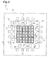
Fig. 2 is a plan view of a composite sensor; -
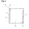
Fig. 3 is a plan view of a thermal image sensor; -
Fig. 4 is a circuit diagram of a range image sensor; -
Fig. 5 is a set of diagrams illustrating steps of manufacturing the composite sensor depicted inFig. 1 ; -
Fig. 6 is a set of diagrams illustrating steps subsequent toFig. 5 ; -
Fig. 7 is a sectional view illustrating the composite sensor module in accordance with a second embodiment of the present invention; -
Fig. 8 is a set of diagrams illustrating steps of manufacturing the composite sensor depicted inFig. 7 ; and -
Fig. 9 is a set of diagrams illustrating steps subsequent toFig. 8 . - In the following, preferred embodiments of the composite sensor and composite sensor module in accordance with the present invention will be explained in detail with reference to the drawings.
-
Fig. 1 is a sectional view illustrating the composite sensor module in accordance with a first embodiment of the present invention. As depicted, thiscomposite sensor module 1 comprises acomposite sensor 11 and alens 12. Thecomposite sensor module 1 is a module used as a motion sensor which detects entries of people into a predetermined area and the like according to thermal and range images. - Connected to the
composite sensor module 1 in use is alight source unit 5 including alight source 2 such as a laser or a light-emitting diode, for example, a lightsource drive circuit 3 for driving thelight source 2 at a high frequency, and a control circuit 4 for outputting a driving clock for the lightsource drive circuit 3. Thelight source 2 emits a modulated wave subjected to light intensity modulation in the form of a square wave or sine wave. The modulated wave is reflected by a surface of an object to be detected K and enters thecomposite sensor 11 through thelens 12. Preferably, the light emitted from thelight source 2 is not visible light, but falls in a wavelength band where a sufficient sensitivity for Si is obtained; for example, near-infrared light having a wavelength of about 800 nm is chosen. The modulated signal (charge transfer signal) in the form of the square wave or sine wave in synchronization with the driving clock from the control circuit 4 is fed to transferelectrodes range image sensor 31, which will be explained later, in respective phases on the reverse of each other. - The
lens 12, which is an imaging lens made of ZnSe, for example, is arranged such as to have an imaging plane at an arrangement region R2 ofrange image sensors 31, which will be explained later. For example, light in a wavelength band of 0.5 µm to 28.1 µm passes through thelens 12, so as to enter thecomposite sensor 11. Not only ZnSe, but ZnS, As2S3, and the like may also be used as a material for thelens 12. - The
composite sensor 11 will now be explained. - As illustrated in
Figs. 1 and2 , thecomposite sensor 11 comprises afirst substrate 13 on whichthermal image sensors 16 are arranged in a matrix and asecond substrate 14, slightly smaller than thefirst substrate 13, on which rangeimage sensors 31 are arranged in a matrix. Each of the first andsecond substrates - An arrangement region R1 of the
thermal image sensors 16 is set into a substantially square form on one side of thefirst substrate 13. On the outside of the arrangement region R1,electrode pads 17 for thethermal image sensors 16 are arranged so as to surround the arrangement region R1.Wires 18 electrically connect theelectrode pads 18 to wiring circuits on the package side. Except for the locations formed with theelectrode pads 17, the one side of thefirst substrate 13 is covered with an insulatingfilm 19 made of SiO2, for example. - Each of the
thermal image sensors 16 arranged on thefirst substrate 13 is a wavelength-independent sensor such as a thermopile or bolometer, for example, and has a plurality of thermoelectric elements. As illustrated inFig. 3 , each pixel of thethermal image sensor 16 has a substantially rectangular light-receivingpart 20, joints 21, 21 extending from two opposing corners of the light-receivingpart 20 in respective directions opposite from each other along sides of the light-receivingpart 20, and supportcolumns joints - Consequently, as illustrated in
Fig. 1 , the light-receivingparts 20 are raised from one side of thefirst substrate 13 while being slightly separated from the insulatingfilm 19. As illustrated inFig. 2 , thethermal image sensors film 19 so as to correspond to the region formed with the light-receivingparts 20. In this case, the light-reflecting layer can make leak light incident on the light-receivingparts 20, thereby further improving the sensitivity of thethermal image sensors 16. - On one side of the
second substrate 14, on the other hand, the arrangement region R2 of thethermal image sensors 31 is set into a substantially square form with a size on a par with the arrangement region R1 of thethermal image sensors 16, for example, as illustrated inFig. 1 . On the outside of the arrangement region R2, theelectrode pads 32 for therange image sensors 31 are arranged so as to surround the arrangement region R2 at positions on the inside of theelectrode pads 32 for thethermal image sensors 31 in planar view. As with theelectrode pads 17, theelectrode pads 32 are electrically connected to wiring circuits on the package side withwires 33. Except for the locations formed with theelectrode pads 32, the one side of thesecond substrate 14 is covered with an insulatingfilm 34 made of SiO2, for example. - The other side of the
second substrate 14 is formed with adepression 36 having a substantially square cross section with a size corresponding to the arrangement region R1 of thethermal image sensors 16 by anisotropic etching or dry etching of Si, for example. The inner wall surface of thedepression 36 is provided with anoptical filter film 37 transparent to light in a mid-infrared region. More specifically, theoptical filter film 37 is constituted by a multilayer film of Ge and ZnS, for example, so as to transmit therethrough only light in a band on the order of 8 µm to 14 µm. On the other side of thesecond substrate 14, fringe parts of thedepression 36 are provided with an insulatingfilm 38 made of SiO2, for example. - The foregoing
second substrate 14 is mounted on thefirst substrate 13 such that thedepression 36 faces thefirst substrate 36, while the arrangement region R1 of thethermal image sensors 16 and the arrangement region R2 of therange image sensors 31 overlap each other as seen in the mounting direction. Mounting thesecond substrate 14 causes the inner wall surface of thedepression 36 and one side of thefirst substrate 13 to form a seal body S1 which seals a space about thethermal image sensors 16 with thefirst substrate 13 serving as a top plate. For mounting the first andsecond substrates thermal image sensors 16 is in a vacuum state. - The
range image sensors 31 arranged on thesecond substrate 14 are so-called charge distribution type range image sensors. As illustrated inFig. 4 , each pixel of therange image sensors 31 has a light-receiving part (charge generation region) 41 for generating an electric charge in response to light incident thereon and a pair oftransfer electrodes part 41 to chargecollection regions - The light-receiving
parts 41, which are parts where the light transmitted through thelens 12 is incident, are arranged 2 × 2 for each light-receivingpart 20 of thethermal image sensors 16 as illustrated inFig. 2 . As a consequence, therange image sensors thermal image sensors parts 41 is formed with a light-shieldingpart 44 made of Al, for example. The light-shieldingpart 44 is formed on the insulatingfilm 34 such as to open at the portion corresponding to the light-receivingparts 41, so that the ratio of the opening portion to the light-shieldingpart 44 is on the order of 20% to 50%, for example. - As illustrated in
Fig. 4 , thecharge collection regions charge collection regions Source follower amplifiers charge collection regions - The
transfer electrodes part 41 and thecharge collection regions transfer electrodes part 41 is formed directly under thetransfer electrode 43 fed with the high-level modulated signal. As a consequence, the electrons generated in the light-receivingpart 41 are transferred by thetransfer electrode 43, so as to be distributed and stored into its correspondingcharge collection region 42. - The electric charges stored in the
charge collection regions source follower amplifiers source follower amplifiers - Steps of manufacturing the
composite sensor 11 will now be explained. - For manufacturing the
composite sensor 11, the first andsecond substrates Fig. 5(a) . Theelectrode pads 17 and insulatingfilm 19 are formed beforehand as a pattern on thefirst substrate 13, and thethermal image sensors 16 are arranged in the arrangement region R1. Thesecond substrate 14 is formed with thedepression 36 by anisotropic etching or dry etching of Si, and then theoptical filter film 37 is formed on the inner wall surface of thedepression 36 by vapor deposition and the like. Thereafter, individual constituents of theelectrode pads 32, insulatingfilms part 44, andrange image sensors 31 are formed as a pattern. - Subsequently, as illustrated in
Fig. 5(b) , thesecond substrate 14 is mounted on thefirst substrate 13 by room temperature bonding such that thedepression 36 faces thefirst substrate 13, while the arrangement region R1 of thethermal image sensors 16 and the arrangement region R2 of therange image sensors 31 overlap each other as seen in the mounting direction. This forms the seal body S1 sealing a space about thethermal image sensors 16 with thefirst substrate 13 serving as a top plate. Joining thesecond substrate 14 to thefirst substrate 13 at room temperature in a vacuum atmosphere can make the seal body S1 have a vacuum state therewithin. - After mounting the
second substrate 14 on thefirst substrate 13, the first andsecond substrates Fig. 6(a) , so as to form modifiedlayers 48 therewithin. From the viewpoint of workability, it is preferred for thefirst substrate 13 to be formed with the modifiedlayers 48 before thesecond substrate 14. - After forming the modified layers 48, an
expandable sheet 49 is attached to the other side of thesecond substrate 14, for example. Then, theexpandable sheet 49 is expanded in its in-plane directions, so as to cut the first andsecond substrates layers 48 as illustrated inFig. 6(b) . This separates the individual devices of thecomposite sensors 11 from each other, thereby yielding thecomposite sensor 11 illustrated inFig. 1 . - In this
composite sensor 11, as explained in the foregoing, the arrangement region R1 of thethermal image sensors 16 and the arrangement region R2 of therange image sensors 31 are arranged so as to overlap each other as seen in the mounting direction. This makes it possible to acquire thermal and range images coaxially, thereby suppressing image misalignment between the thermal and range images. Hence, an object to be detected can be detected accurately. It also reduces the time required for calculations and improves time resolution. - In this
composite sensor 11, the seal body S1 formed by mounting the first andsecond substrates thermal image sensors 16 in a vacuum state. This can prevent the heat occurring about therange image sensors 31 from affecting thethermal image sensor 16 side, thereby improving the sensitivity of thethermal image sensors 16. In addition, the substrate arranged with thethermal image sensors 16 and the substrate arranged with therange image sensors 31 are separate from each other, which makes it possible to perform manufacturing methods optimal for the sensors and secure a degree of freedom in designing for arranging a signal readout circuit and the like. - In the
composite sensor 11, the arrangement pitch W2 of therange image sensors 31 in thesecond substrate 14 is smaller than the arrangement pitch W1 of thethermal image sensors 16 in thefirst substrate 13. Therange image sensors 31 include constituents such as thetransfer electrodes 43, and these constituents may become a shield which covers thethermal image sensors 16. Therefore, when the arrangement pitch W2 of therange image sensors 31 is on a par with or greater than the arrangement pitch W1 of thethermal image sensors 16, the influence of shield per pixel of thethermal image sensors 16 may be so large that thermal images deteriorate their quality. Hence, making the arrangement pitch W2 of therange image sensors 31 smaller than the arrangement pitch W1 of thethermal image sensors 16 can suppress the influence of shield per pixel of thethermal image sensors 16, thereby securing the thermal image quality. - In the
composite sensor 11, theoptical filter film 37 transparent to light in a mid-infrared region is formed on an inner wall surface of theseal body S 1. This can cut off light in a wavelength band which is susceptible to the absorption by moisture, carbon dioxide, and the like in air, thereby enabling thethermal image sensors 16 to further improve their sensitivity. -
Fig. 7 is a sectional view illustrating acomposite sensor module 50 in accordance with a second embodiment of the present invention. As depicted, thecomposite sensor module 50 in accordance with the second embodiment differs from the first embodiment in the joint structure between the first andsecond substrates composite sensor 51. - More specifically, the
composite sensor 51 has nodepression 36 on the other side of thesecond substrate 14, so that thesecond substrate 14 has a flat surface on the other side. Theoptical filter film 37 is formed all over the surface on the other side of thesecond substrate 14. For joining the first andsecond substrates materials 52 and alid material 53 are used. Thefoil materials 52, each of which is a layer combining a buffer metal with a low-melting metal, are made of Ti/Pt/Au or Cr/Ni/Au, for example. Thefoil materials 52 are arranged like rings on one side of thefirst substrate 13 and the other side of thesecond substrate 14 at positions overlapping theelectrode pads 32, for example. - The
lid material 53 is a ring-shaped metal material made of Kovar, for example. Thelid material 53 is held between and joined to thefoil material 52 on thefirst substrate 13 side and thefoil material 52 on the second substrate side. Since thelid material 53 is interposed, a space corresponding to the thickness of thelid material 53 is formed between the first andsecond substrates first substrate 13, the other side of thesecond substrate 14, and thelid material 53 form a seal body S2 sealing a space about thethermal image sensors 16 with thefirst substrate 13 serving as a top plate. The inner space of the seal body S2 has a vacuum state as in the first embodiment. - For manufacturing the
composite sensor 51, the first andsecond substrates Fig. 8(a) . Theelectrode pads 17, insulatingfilm 19, and foilmaterial 52 are formed beforehand as a pattern on thefirst substrate 13, and thethermal image sensors 16 are arranged in the arrangement region R1. Thesecond substrate 14 is formed beforehand with individual constituents of theelectrode pads 32, insulatingfilms foil material 52, light-shieldingpart 44, andrange image sensors 31 as a pattern after forming theoptical filter film 37 on the other side by vapor deposition, for example. - Subsequently, as illustrated in
Fig. 8(b) , thelid material 53 is arranged between thefoil materials thermal image sensors 16 and the arrangement region R2 of therange image sensors 31 overlap each other as seen in the mounting direction, and thesecond substrate 14 is mounted on thefirst substrate 13. This forms the seal body S2 sealing a space about thethermal image sensors 16 with thefirst substrate 13 serving as a top plate. Joining them in a vacuum atmosphere can place the inner space of the seal body S2 into a vacuum state. - After mounting the
second substrate 14 on thefirst substrate 13, the first andsecond substrates Fig. 9(a) , so as to form modifiedlayers 54 therewithin. From the viewpoint of workability, it is preferred for thefirst substrate 13 to be formed with the modifiedlayers 54 before thesecond substrate 14. - After forming the modified layers 54, an
expandable sheet 49 is attached to the other side of thesecond substrate 14, for example. Then, theexpandable sheet 49 is expanded in its in-plane directions, so as to cut the first andsecond substrates layers 54 as illustrated inFig. 9(b) . This separates the individual devices of thecomposite sensor 51 from each other, thereby yielding thecomposite sensor 51 illustrated inFig. 7 . - In the foregoing
composite sensor 51, the arrangement region R1 of thethermal image sensors 16 and the arrangement region R2 of therange image sensors 31 are also arranged so as to overlap each other as seen in the mounting direction. This makes it possible to acquire thermal and range images coaxially, thereby suppressing image misalignment between the thermal and range images. Hence, an object to be detected can be detected accurately. It also reduces the time required for calculations and improves time resolution. - In this
composite sensor 51, the seal body S2 formed by mounting the first andsecond substrates thermal image sensors 16 in a vacuum state. This can prevent the heat occurring about therange image sensors 31 from affecting thethermal image sensor 16 side, thereby improving the sensitivity of thethermal image sensors 16. In addition, the substrate arranged with thethermal image sensors 16 and the substrate arranged with therange image sensors 31 are separate from each other, which makes it possible to perform manufacturing methods optimal for the sensors and secure a degree of freedom in designing for arranging a signal readout circuit and the like. - In this
composite sensor 51, the arrangement pitch W2 of therange image sensors 31 in thesecond substrate 14 is also smaller than the arrangement pitch W1 of thethermal image sensors 16 in thefirst substrate 13. This can suppress the influence of shield per pixel of thethermal image sensors 16, thereby securing the thermal image quality. Further, theoptical filter film 37 within the seal body S2 can cut off light in a wavelength band which is susceptible to the absorption by moisture, carbon dioxide, and the like in air, thereby enabling thethermal image sensors 16 to further improve their sensitivity. - 1, 50: composite sensor module; 11, 51: composite sensor; 12: lens; 13: first substrate; 14: second substrate; 16: thermal image sensor; 31: range image sensor; 37: optical filter film; 41: light-receiving part (charge generation region); 42: charge collection region; 43: transfer electrode; R1: arrangement region of thermal image sensors; R2: arrangement region of range image sensors; S1, S2: seal body; W1: arrangement pitch of thermal image sensors; W2: arrangement pitch of range image sensors.
Claims (5)
- A composite sensor comprising:a first substrate arranged with a thermal image sensor constituted by a plurality of thermoelectric elements; anda second substrate arranged with a range image sensor having a charge generation region for generating an electric charge in response to light incident thereon and a transfer electrode for transferring the electric charge generated in the charge generation region to a predetermined charge collection region according to a charge transfer signal given beforehand;wherein the second substrate is mounted on the first substrate such that a region arranged with the thermal image sensor and a region arranged with the range image sensor overlap each other as seen in the mounting direction; andwherein the first and second substrates are mounted on top of each other so as to form a seal body sealing a space about the thermal image sensor with the first substrate serving as a top plate.
- A composite sensor according to claim 1, wherein the range image sensor in the second substrate has an arrangement pitch smaller than that of the thermal image sensor in the first substrate.
- A composite sensor according to claim 1 or 2, wherein an optical filter film transparent to light in a mid-infrared region is formed on an inner wall surface of the seal body.
- A composite sensor according to one of claims 1 to 3, wherein the seal body has a vacuum state therewithin.
- A composite sensor module comprising:the composite sensor according to one of claims 1 to 4; anda lens arranged such as to have an imaging plane at the region arranged with the range image sensor in the second substrate.
Applications Claiming Priority (2)
| Application Number | Priority Date | Filing Date | Title |
|---|---|---|---|
| JP2012171340A JP5909421B2 (en) | 2012-08-01 | 2012-08-01 | Composite sensor and composite sensor module |
| PCT/JP2013/061296 WO2014020950A1 (en) | 2012-08-01 | 2013-04-16 | Composite sensor and composite sensor module |
Publications (3)
| Publication Number | Publication Date |
|---|---|
| EP2881761A1 true EP2881761A1 (en) | 2015-06-10 |
| EP2881761A4 EP2881761A4 (en) | 2016-05-25 |
| EP2881761B1 EP2881761B1 (en) | 2017-05-17 |
Family
ID=50027645
Family Applications (1)
| Application Number | Title | Priority Date | Filing Date |
|---|---|---|---|
| EP13825122.8A Not-in-force EP2881761B1 (en) | 2012-08-01 | 2013-04-16 | Composite sensor and composite sensor module |
Country Status (7)
| Country | Link |
|---|---|
| US (1) | US9476773B2 (en) |
| EP (1) | EP2881761B1 (en) |
| JP (1) | JP5909421B2 (en) |
| KR (1) | KR101994508B1 (en) |
| CN (1) | CN104508441B (en) |
| TW (1) | TWI576982B (en) |
| WO (1) | WO2014020950A1 (en) |
Families Citing this family (8)
| Publication number | Priority date | Publication date | Assignee | Title |
|---|---|---|---|---|
| US11405569B2 (en) | 2017-07-25 | 2022-08-02 | Sony Semiconductor Solutions Corporation | Solid-state imaging device |
| WO2020254152A1 (en) * | 2019-06-18 | 2020-12-24 | Ams International Ag | Time of flight sensors with light directing elements |
| JP1701619S (en) | 2021-01-20 | 2021-12-06 | ||
| JP1712335S (en) | 2021-01-20 | 2022-04-12 | Light emitting element module | |
| USD1089808S1 (en) | 2021-01-20 | 2025-08-19 | Hamamatsu Photonics K.K. | Light-emitting element module |
| USD1083850S1 (en) * | 2021-01-20 | 2025-07-15 | Hamamatsu Photonics K.K. | Light-emitting element module |
| JP1701505S (en) | 2021-01-20 | 2021-12-06 | ||
| WO2026014062A1 (en) * | 2024-07-09 | 2026-01-15 | ソニーセミコンダクタソリューションズ株式会社 | Light detection sensor, light detection device, and electronic apparatus |
Family Cites Families (12)
| Publication number | Priority date | Publication date | Assignee | Title |
|---|---|---|---|---|
| JPH11214668A (en) * | 1997-11-20 | 1999-08-06 | Nikon Corp | Solid-state imaging device and light receiving element |
| JP2001318165A (en) * | 2000-05-08 | 2001-11-16 | Seiko Precision Inc | Sensor module |
| JP5283825B2 (en) | 2006-01-25 | 2013-09-04 | 浜松ホトニクス株式会社 | Thermal infrared detector |
| WO2007086421A1 (en) * | 2006-01-26 | 2007-08-02 | National University Corporation Hokkaido University | Honeycomb type porous article usable in regeneration therapy for hard tissues |
| EP2924465B1 (en) | 2007-07-03 | 2017-11-29 | Hamamatsu Photonics K.K. | Back-illuminated distance measuring sensor and distance measuring device |
| JP4971890B2 (en) * | 2007-07-03 | 2012-07-11 | 浜松ホトニクス株式会社 | Back-illuminated distance measuring sensor and distance measuring device |
| FR2927196B1 (en) | 2008-02-01 | 2010-02-12 | Commissariat Energie Atomique | PIXEL FOR 3D ACTIVE IMAGING. |
| JP5136110B2 (en) | 2008-02-19 | 2013-02-06 | ソニー株式会社 | Method for manufacturing solid-state imaging device |
| JP5620087B2 (en) * | 2009-11-30 | 2014-11-05 | 浜松ホトニクス株式会社 | Distance sensor and distance image sensor |
| JP5445963B2 (en) * | 2010-04-28 | 2014-03-19 | 国立大学法人 東京大学 | Optical element and imaging device |
| JP5589605B2 (en) | 2010-06-25 | 2014-09-17 | セイコーエプソン株式会社 | Pyroelectric detector, pyroelectric detector and electronic device |
| CN102564601A (en) * | 2010-12-22 | 2012-07-11 | 精工爱普生株式会社 | Thermal detector, thermal detection device, electronic instrument, and thermal detector manufacturing method |
-
2012
- 2012-08-01 JP JP2012171340A patent/JP5909421B2/en not_active Expired - Fee Related
-
2013
- 2013-04-16 US US14/415,868 patent/US9476773B2/en active Active
- 2013-04-16 WO PCT/JP2013/061296 patent/WO2014020950A1/en not_active Ceased
- 2013-04-16 KR KR1020147027680A patent/KR101994508B1/en not_active Expired - Fee Related
- 2013-04-16 CN CN201380041019.4A patent/CN104508441B/en not_active Expired - Fee Related
- 2013-04-16 EP EP13825122.8A patent/EP2881761B1/en not_active Not-in-force
- 2013-05-14 TW TW102117094A patent/TWI576982B/en not_active IP Right Cessation
Also Published As
| Publication number | Publication date |
|---|---|
| CN104508441A (en) | 2015-04-08 |
| KR101994508B1 (en) | 2019-06-28 |
| US9476773B2 (en) | 2016-10-25 |
| JP2014032045A (en) | 2014-02-20 |
| TW201407746A (en) | 2014-02-16 |
| EP2881761B1 (en) | 2017-05-17 |
| EP2881761A4 (en) | 2016-05-25 |
| JP5909421B2 (en) | 2016-04-26 |
| TWI576982B (en) | 2017-04-01 |
| KR20150039707A (en) | 2015-04-13 |
| CN104508441B (en) | 2017-03-08 |
| US20150211935A1 (en) | 2015-07-30 |
| WO2014020950A1 (en) | 2014-02-06 |
Similar Documents
| Publication | Publication Date | Title |
|---|---|---|
| EP2881761B1 (en) | Composite sensor and composite sensor module | |
| US9587978B2 (en) | Infrared sensor | |
| CN103839952B (en) | Image sensing device | |
| KR102661190B1 (en) | light detection device | |
| US10078007B2 (en) | Infrared sensor | |
| CN109690777B (en) | Distance sensor and distance image sensor | |
| JP5662225B2 (en) | Infrared sensor | |
| JP5636557B2 (en) | Infrared sensor manufacturing method, infrared sensor, and quantum infrared gas concentration meter | |
| JP2013041921A (en) | Vacuum sealing device | |
| US10816406B2 (en) | Infrared detector pixel structure and manufactureing method thereof | |
| JP2006317232A (en) | Infrared sensor | |
| JP2013079852A (en) | Optical sensor module and optical sensor | |
| JP2013190243A (en) | Sensor device | |
| JP4740022B2 (en) | Optical sensor and object detection method | |
| JP2012230010A (en) | Infrared sensor | |
| JP2005207830A (en) | Infrared sensor | |
| WO2011121706A1 (en) | Infrared ray imaging element and infrared ray imaging device | |
| JP2013195371A (en) | Sensor device | |
| JP2016090377A (en) | Infrared sensor | |
| JP2007127496A (en) | Thermal infrared detector | |
| JPS62184423A (en) | Distance measuring device | |
| JP2012198096A (en) | Infrared sensor module |
Legal Events
| Date | Code | Title | Description |
|---|---|---|---|
| PUAI | Public reference made under article 153(3) epc to a published international application that has entered the european phase |
Free format text: ORIGINAL CODE: 0009012 |
|
| 17P | Request for examination filed |
Effective date: 20140905 |
|
| AK | Designated contracting states |
Kind code of ref document: A1 Designated state(s): AL AT BE BG CH CY CZ DE DK EE ES FI FR GB GR HR HU IE IS IT LI LT LU LV MC MK MT NL NO PL PT RO RS SE SI SK SM TR |
|
| AX | Request for extension of the european patent |
Extension state: BA ME |
|
| DAX | Request for extension of the european patent (deleted) | ||
| RA4 | Supplementary search report drawn up and despatched (corrected) |
Effective date: 20160421 |
|
| RIC1 | Information provided on ipc code assigned before grant |
Ipc: H04N 5/374 20110101ALI20160415BHEP Ipc: H04N 5/335 20060101ALI20160415BHEP Ipc: G01S 17/02 20060101ALI20160415BHEP Ipc: G01J 5/08 20060101ALI20160415BHEP Ipc: H01L 27/146 20060101ALI20160415BHEP Ipc: G01C 3/02 20060101ALI20160415BHEP Ipc: G01J 3/36 20060101ALI20160415BHEP Ipc: G01J 5/04 20060101ALI20160415BHEP Ipc: H04N 5/33 20060101ALI20160415BHEP Ipc: G01S 7/481 20060101ALI20160415BHEP Ipc: G01J 5/02 20060101ALI20160415BHEP Ipc: G01V 8/20 20060101AFI20160415BHEP Ipc: G01B 11/00 20060101ALI20160415BHEP Ipc: G01J 1/02 20060101ALI20160415BHEP |
|
| GRAP | Despatch of communication of intention to grant a patent |
Free format text: ORIGINAL CODE: EPIDOSNIGR1 |
|
| INTG | Intention to grant announced |
Effective date: 20170203 |
|
| INTG | Intention to grant announced |
Effective date: 20170203 |
|
| GRAS | Grant fee paid |
Free format text: ORIGINAL CODE: EPIDOSNIGR3 |
|
| GRAA | (expected) grant |
Free format text: ORIGINAL CODE: 0009210 |
|
| AK | Designated contracting states |
Kind code of ref document: B1 Designated state(s): AL AT BE BG CH CY CZ DE DK EE ES FI FR GB GR HR HU IE IS IT LI LT LU LV MC MK MT NL NO PL PT RO RS SE SI SK SM TR |
|
| REG | Reference to a national code |
Ref country code: GB Ref legal event code: FG4D |
|
| REG | Reference to a national code |
Ref country code: CH Ref legal event code: EP |
|
| REG | Reference to a national code |
Ref country code: IE Ref legal event code: FG4D |
|
| REG | Reference to a national code |
Ref country code: AT Ref legal event code: REF Ref document number: 894964 Country of ref document: AT Kind code of ref document: T Effective date: 20170615 |
|
| REG | Reference to a national code |
Ref country code: DE Ref legal event code: R096 Ref document number: 602013021398 Country of ref document: DE |
|
| REG | Reference to a national code |
Ref country code: NL Ref legal event code: MP Effective date: 20170517 |
|
| REG | Reference to a national code |
Ref country code: LT Ref legal event code: MG4D |
|
| REG | Reference to a national code |
Ref country code: AT Ref legal event code: MK05 Ref document number: 894964 Country of ref document: AT Kind code of ref document: T Effective date: 20170517 |
|
| PG25 | Lapsed in a contracting state [announced via postgrant information from national office to epo] |
Ref country code: HR Free format text: LAPSE BECAUSE OF FAILURE TO SUBMIT A TRANSLATION OF THE DESCRIPTION OR TO PAY THE FEE WITHIN THE PRESCRIBED TIME-LIMIT Effective date: 20170517 Ref country code: NO Free format text: LAPSE BECAUSE OF FAILURE TO SUBMIT A TRANSLATION OF THE DESCRIPTION OR TO PAY THE FEE WITHIN THE PRESCRIBED TIME-LIMIT Effective date: 20170817 Ref country code: AT Free format text: LAPSE BECAUSE OF FAILURE TO SUBMIT A TRANSLATION OF THE DESCRIPTION OR TO PAY THE FEE WITHIN THE PRESCRIBED TIME-LIMIT Effective date: 20170517 Ref country code: GR Free format text: LAPSE BECAUSE OF FAILURE TO SUBMIT A TRANSLATION OF THE DESCRIPTION OR TO PAY THE FEE WITHIN THE PRESCRIBED TIME-LIMIT Effective date: 20170818 Ref country code: LT Free format text: LAPSE BECAUSE OF FAILURE TO SUBMIT A TRANSLATION OF THE DESCRIPTION OR TO PAY THE FEE WITHIN THE PRESCRIBED TIME-LIMIT Effective date: 20170517 Ref country code: ES Free format text: LAPSE BECAUSE OF FAILURE TO SUBMIT A TRANSLATION OF THE DESCRIPTION OR TO PAY THE FEE WITHIN THE PRESCRIBED TIME-LIMIT Effective date: 20170517 Ref country code: FI Free format text: LAPSE BECAUSE OF FAILURE TO SUBMIT A TRANSLATION OF THE DESCRIPTION OR TO PAY THE FEE WITHIN THE PRESCRIBED TIME-LIMIT Effective date: 20170517 |
|
| PG25 | Lapsed in a contracting state [announced via postgrant information from national office to epo] |
Ref country code: PL Free format text: LAPSE BECAUSE OF FAILURE TO SUBMIT A TRANSLATION OF THE DESCRIPTION OR TO PAY THE FEE WITHIN THE PRESCRIBED TIME-LIMIT Effective date: 20170517 Ref country code: NL Free format text: LAPSE BECAUSE OF FAILURE TO SUBMIT A TRANSLATION OF THE DESCRIPTION OR TO PAY THE FEE WITHIN THE PRESCRIBED TIME-LIMIT Effective date: 20170517 Ref country code: BG Free format text: LAPSE BECAUSE OF FAILURE TO SUBMIT A TRANSLATION OF THE DESCRIPTION OR TO PAY THE FEE WITHIN THE PRESCRIBED TIME-LIMIT Effective date: 20170817 Ref country code: SE Free format text: LAPSE BECAUSE OF FAILURE TO SUBMIT A TRANSLATION OF THE DESCRIPTION OR TO PAY THE FEE WITHIN THE PRESCRIBED TIME-LIMIT Effective date: 20170517 Ref country code: RS Free format text: LAPSE BECAUSE OF FAILURE TO SUBMIT A TRANSLATION OF THE DESCRIPTION OR TO PAY THE FEE WITHIN THE PRESCRIBED TIME-LIMIT Effective date: 20170517 Ref country code: LV Free format text: LAPSE BECAUSE OF FAILURE TO SUBMIT A TRANSLATION OF THE DESCRIPTION OR TO PAY THE FEE WITHIN THE PRESCRIBED TIME-LIMIT Effective date: 20170517 Ref country code: IS Free format text: LAPSE BECAUSE OF FAILURE TO SUBMIT A TRANSLATION OF THE DESCRIPTION OR TO PAY THE FEE WITHIN THE PRESCRIBED TIME-LIMIT Effective date: 20170917 |
|
| PG25 | Lapsed in a contracting state [announced via postgrant information from national office to epo] |
Ref country code: EE Free format text: LAPSE BECAUSE OF FAILURE TO SUBMIT A TRANSLATION OF THE DESCRIPTION OR TO PAY THE FEE WITHIN THE PRESCRIBED TIME-LIMIT Effective date: 20170517 Ref country code: CZ Free format text: LAPSE BECAUSE OF FAILURE TO SUBMIT A TRANSLATION OF THE DESCRIPTION OR TO PAY THE FEE WITHIN THE PRESCRIBED TIME-LIMIT Effective date: 20170517 Ref country code: RO Free format text: LAPSE BECAUSE OF FAILURE TO SUBMIT A TRANSLATION OF THE DESCRIPTION OR TO PAY THE FEE WITHIN THE PRESCRIBED TIME-LIMIT Effective date: 20170517 Ref country code: DK Free format text: LAPSE BECAUSE OF FAILURE TO SUBMIT A TRANSLATION OF THE DESCRIPTION OR TO PAY THE FEE WITHIN THE PRESCRIBED TIME-LIMIT Effective date: 20170517 Ref country code: SK Free format text: LAPSE BECAUSE OF FAILURE TO SUBMIT A TRANSLATION OF THE DESCRIPTION OR TO PAY THE FEE WITHIN THE PRESCRIBED TIME-LIMIT Effective date: 20170517 |
|
| REG | Reference to a national code |
Ref country code: DE Ref legal event code: R097 Ref document number: 602013021398 Country of ref document: DE |
|
| PG25 | Lapsed in a contracting state [announced via postgrant information from national office to epo] |
Ref country code: SM Free format text: LAPSE BECAUSE OF FAILURE TO SUBMIT A TRANSLATION OF THE DESCRIPTION OR TO PAY THE FEE WITHIN THE PRESCRIBED TIME-LIMIT Effective date: 20170517 Ref country code: IT Free format text: LAPSE BECAUSE OF FAILURE TO SUBMIT A TRANSLATION OF THE DESCRIPTION OR TO PAY THE FEE WITHIN THE PRESCRIBED TIME-LIMIT Effective date: 20170517 |
|
| REG | Reference to a national code |
Ref country code: FR Ref legal event code: PLFP Year of fee payment: 6 |
|
| PLBE | No opposition filed within time limit |
Free format text: ORIGINAL CODE: 0009261 |
|
| STAA | Information on the status of an ep patent application or granted ep patent |
Free format text: STATUS: NO OPPOSITION FILED WITHIN TIME LIMIT |
|
| 26N | No opposition filed |
Effective date: 20180220 |
|
| PG25 | Lapsed in a contracting state [announced via postgrant information from national office to epo] |
Ref country code: SI Free format text: LAPSE BECAUSE OF FAILURE TO SUBMIT A TRANSLATION OF THE DESCRIPTION OR TO PAY THE FEE WITHIN THE PRESCRIBED TIME-LIMIT Effective date: 20170517 |
|
| PG25 | Lapsed in a contracting state [announced via postgrant information from national office to epo] |
Ref country code: MC Free format text: LAPSE BECAUSE OF FAILURE TO SUBMIT A TRANSLATION OF THE DESCRIPTION OR TO PAY THE FEE WITHIN THE PRESCRIBED TIME-LIMIT Effective date: 20170517 |
|
| REG | Reference to a national code |
Ref country code: CH Ref legal event code: PL |
|
| REG | Reference to a national code |
Ref country code: BE Ref legal event code: MM Effective date: 20180430 |
|
| GBPC | Gb: european patent ceased through non-payment of renewal fee |
Effective date: 20180416 |
|
| REG | Reference to a national code |
Ref country code: IE Ref legal event code: MM4A |
|
| PG25 | Lapsed in a contracting state [announced via postgrant information from national office to epo] |
Ref country code: LU Free format text: LAPSE BECAUSE OF NON-PAYMENT OF DUE FEES Effective date: 20180416 |
|
| PG25 | Lapsed in a contracting state [announced via postgrant information from national office to epo] |
Ref country code: CH Free format text: LAPSE BECAUSE OF NON-PAYMENT OF DUE FEES Effective date: 20180430 Ref country code: BE Free format text: LAPSE BECAUSE OF NON-PAYMENT OF DUE FEES Effective date: 20180430 Ref country code: LI Free format text: LAPSE BECAUSE OF NON-PAYMENT OF DUE FEES Effective date: 20180430 Ref country code: GB Free format text: LAPSE BECAUSE OF NON-PAYMENT OF DUE FEES Effective date: 20180416 |
|
| PG25 | Lapsed in a contracting state [announced via postgrant information from national office to epo] |
Ref country code: IE Free format text: LAPSE BECAUSE OF NON-PAYMENT OF DUE FEES Effective date: 20180416 |
|
| PG25 | Lapsed in a contracting state [announced via postgrant information from national office to epo] |
Ref country code: MT Free format text: LAPSE BECAUSE OF NON-PAYMENT OF DUE FEES Effective date: 20180416 |
|
| PG25 | Lapsed in a contracting state [announced via postgrant information from national office to epo] |
Ref country code: TR Free format text: LAPSE BECAUSE OF FAILURE TO SUBMIT A TRANSLATION OF THE DESCRIPTION OR TO PAY THE FEE WITHIN THE PRESCRIBED TIME-LIMIT Effective date: 20170517 |
|
| PG25 | Lapsed in a contracting state [announced via postgrant information from national office to epo] |
Ref country code: PT Free format text: LAPSE BECAUSE OF FAILURE TO SUBMIT A TRANSLATION OF THE DESCRIPTION OR TO PAY THE FEE WITHIN THE PRESCRIBED TIME-LIMIT Effective date: 20170517 |
|
| PG25 | Lapsed in a contracting state [announced via postgrant information from national office to epo] |
Ref country code: HU Free format text: LAPSE BECAUSE OF FAILURE TO SUBMIT A TRANSLATION OF THE DESCRIPTION OR TO PAY THE FEE WITHIN THE PRESCRIBED TIME-LIMIT; INVALID AB INITIO Effective date: 20130416 Ref country code: CY Free format text: LAPSE BECAUSE OF FAILURE TO SUBMIT A TRANSLATION OF THE DESCRIPTION OR TO PAY THE FEE WITHIN THE PRESCRIBED TIME-LIMIT Effective date: 20170517 Ref country code: MK Free format text: LAPSE BECAUSE OF NON-PAYMENT OF DUE FEES Effective date: 20170517 |
|
| PG25 | Lapsed in a contracting state [announced via postgrant information from national office to epo] |
Ref country code: AL Free format text: LAPSE BECAUSE OF FAILURE TO SUBMIT A TRANSLATION OF THE DESCRIPTION OR TO PAY THE FEE WITHIN THE PRESCRIBED TIME-LIMIT Effective date: 20170517 |
|
| P01 | Opt-out of the competence of the unified patent court (upc) registered |
Effective date: 20230517 |
|
| PGFP | Annual fee paid to national office [announced via postgrant information from national office to epo] |
Ref country code: FR Payment date: 20240308 Year of fee payment: 12 |
|
| PGFP | Annual fee paid to national office [announced via postgrant information from national office to epo] |
Ref country code: DE Payment date: 20240227 Year of fee payment: 12 |
|
| REG | Reference to a national code |
Ref country code: DE Ref legal event code: R119 Ref document number: 602013021398 Country of ref document: DE |
|
| PG25 | Lapsed in a contracting state [announced via postgrant information from national office to epo] |
Ref country code: DE Free format text: LAPSE BECAUSE OF NON-PAYMENT OF DUE FEES Effective date: 20251104 |
|
| PG25 | Lapsed in a contracting state [announced via postgrant information from national office to epo] |
Ref country code: FR Free format text: LAPSE BECAUSE OF NON-PAYMENT OF DUE FEES Effective date: 20250430 |