EP2876695A1 - Solar cell - Google Patents
Solar cell Download PDFInfo
- Publication number
- EP2876695A1 EP2876695A1 EP14193971.0A EP14193971A EP2876695A1 EP 2876695 A1 EP2876695 A1 EP 2876695A1 EP 14193971 A EP14193971 A EP 14193971A EP 2876695 A1 EP2876695 A1 EP 2876695A1
- Authority
- EP
- European Patent Office
- Prior art keywords
- separation
- electrode
- solar cell
- groove
- grooves
- Prior art date
- Legal status (The legal status is an assumption and is not a legal conclusion. Google has not performed a legal analysis and makes no representation as to the accuracy of the status listed.)
- Withdrawn
Links
Images






Classifications
-
- H—ELECTRICITY
- H10—SEMICONDUCTOR DEVICES; ELECTRIC SOLID-STATE DEVICES NOT OTHERWISE PROVIDED FOR
- H10F—INORGANIC SEMICONDUCTOR DEVICES SENSITIVE TO INFRARED RADIATION, LIGHT, ELECTROMAGNETIC RADIATION OF SHORTER WAVELENGTH OR CORPUSCULAR RADIATION
- H10F10/00—Individual photovoltaic cells, e.g. solar cells
-
- H—ELECTRICITY
- H10—SEMICONDUCTOR DEVICES; ELECTRIC SOLID-STATE DEVICES NOT OTHERWISE PROVIDED FOR
- H10F—INORGANIC SEMICONDUCTOR DEVICES SENSITIVE TO INFRARED RADIATION, LIGHT, ELECTROMAGNETIC RADIATION OF SHORTER WAVELENGTH OR CORPUSCULAR RADIATION
- H10F19/00—Integrated devices, or assemblies of multiple devices, comprising at least one photovoltaic cell covered by group H10F10/00, e.g. photovoltaic modules
- H10F19/90—Structures for connecting between photovoltaic cells, e.g. interconnections or insulating spacers
- H10F19/902—Structures for connecting between photovoltaic cells, e.g. interconnections or insulating spacers for series or parallel connection of photovoltaic cells
- H10F19/904—Structures for connecting between photovoltaic cells, e.g. interconnections or insulating spacers for series or parallel connection of photovoltaic cells characterised by the shapes of the structures
-
- H—ELECTRICITY
- H10—SEMICONDUCTOR DEVICES; ELECTRIC SOLID-STATE DEVICES NOT OTHERWISE PROVIDED FOR
- H10F—INORGANIC SEMICONDUCTOR DEVICES SENSITIVE TO INFRARED RADIATION, LIGHT, ELECTROMAGNETIC RADIATION OF SHORTER WAVELENGTH OR CORPUSCULAR RADIATION
- H10F10/00—Individual photovoltaic cells, e.g. solar cells
- H10F10/10—Individual photovoltaic cells, e.g. solar cells having potential barriers
- H10F10/16—Photovoltaic cells having only PN heterojunction potential barriers
- H10F10/167—Photovoltaic cells having only PN heterojunction potential barriers comprising Group I-III-VI materials, e.g. CdS/CuInSe2 [CIS] heterojunction photovoltaic cells
-
- H—ELECTRICITY
- H10—SEMICONDUCTOR DEVICES; ELECTRIC SOLID-STATE DEVICES NOT OTHERWISE PROVIDED FOR
- H10F—INORGANIC SEMICONDUCTOR DEVICES SENSITIVE TO INFRARED RADIATION, LIGHT, ELECTROMAGNETIC RADIATION OF SHORTER WAVELENGTH OR CORPUSCULAR RADIATION
- H10F19/00—Integrated devices, or assemblies of multiple devices, comprising at least one photovoltaic cell covered by group H10F10/00, e.g. photovoltaic modules
- H10F19/30—Integrated devices, or assemblies of multiple devices, comprising at least one photovoltaic cell covered by group H10F10/00, e.g. photovoltaic modules comprising thin-film photovoltaic cells
- H10F19/31—Integrated devices, or assemblies of multiple devices, comprising at least one photovoltaic cell covered by group H10F10/00, e.g. photovoltaic modules comprising thin-film photovoltaic cells having multiple laterally adjacent thin-film photovoltaic cells deposited on the same substrate
-
- H—ELECTRICITY
- H10—SEMICONDUCTOR DEVICES; ELECTRIC SOLID-STATE DEVICES NOT OTHERWISE PROVIDED FOR
- H10F—INORGANIC SEMICONDUCTOR DEVICES SENSITIVE TO INFRARED RADIATION, LIGHT, ELECTROMAGNETIC RADIATION OF SHORTER WAVELENGTH OR CORPUSCULAR RADIATION
- H10F19/00—Integrated devices, or assemblies of multiple devices, comprising at least one photovoltaic cell covered by group H10F10/00, e.g. photovoltaic modules
- H10F19/30—Integrated devices, or assemblies of multiple devices, comprising at least one photovoltaic cell covered by group H10F10/00, e.g. photovoltaic modules comprising thin-film photovoltaic cells
- H10F19/31—Integrated devices, or assemblies of multiple devices, comprising at least one photovoltaic cell covered by group H10F10/00, e.g. photovoltaic modules comprising thin-film photovoltaic cells having multiple laterally adjacent thin-film photovoltaic cells deposited on the same substrate
- H10F19/35—Structures for the connecting of adjacent photovoltaic cells, e.g. interconnections or insulating spacers
-
- H—ELECTRICITY
- H10—SEMICONDUCTOR DEVICES; ELECTRIC SOLID-STATE DEVICES NOT OTHERWISE PROVIDED FOR
- H10F—INORGANIC SEMICONDUCTOR DEVICES SENSITIVE TO INFRARED RADIATION, LIGHT, ELECTROMAGNETIC RADIATION OF SHORTER WAVELENGTH OR CORPUSCULAR RADIATION
- H10F19/00—Integrated devices, or assemblies of multiple devices, comprising at least one photovoltaic cell covered by group H10F10/00, e.g. photovoltaic modules
- H10F19/30—Integrated devices, or assemblies of multiple devices, comprising at least one photovoltaic cell covered by group H10F10/00, e.g. photovoltaic modules comprising thin-film photovoltaic cells
- H10F19/31—Integrated devices, or assemblies of multiple devices, comprising at least one photovoltaic cell covered by group H10F10/00, e.g. photovoltaic modules comprising thin-film photovoltaic cells having multiple laterally adjacent thin-film photovoltaic cells deposited on the same substrate
- H10F19/37—Integrated devices, or assemblies of multiple devices, comprising at least one photovoltaic cell covered by group H10F10/00, e.g. photovoltaic modules comprising thin-film photovoltaic cells having multiple laterally adjacent thin-film photovoltaic cells deposited on the same substrate comprising means for obtaining partial light transmission through the integrated devices, or the assemblies of multiple devices, e.g. partially transparent thin-film photovoltaic modules for windows
-
- Y—GENERAL TAGGING OF NEW TECHNOLOGICAL DEVELOPMENTS; GENERAL TAGGING OF CROSS-SECTIONAL TECHNOLOGIES SPANNING OVER SEVERAL SECTIONS OF THE IPC; TECHNICAL SUBJECTS COVERED BY FORMER USPC CROSS-REFERENCE ART COLLECTIONS [XRACs] AND DIGESTS
- Y02—TECHNOLOGIES OR APPLICATIONS FOR MITIGATION OR ADAPTATION AGAINST CLIMATE CHANGE
- Y02E—REDUCTION OF GREENHOUSE GAS [GHG] EMISSIONS, RELATED TO ENERGY GENERATION, TRANSMISSION OR DISTRIBUTION
- Y02E10/00—Energy generation through renewable energy sources
- Y02E10/50—Photovoltaic [PV] energy
- Y02E10/541—CuInSe2 material PV cells
Definitions
- the present invention relates generally to a solar cell.
- a solar cell which is a photovoltaic device that converts solar energy into electrical energy, is a next-generation pollution free energy source.
- a solar cell typically includes p-type semiconductor and n-type semiconductor.
- EHP electron-hole pair
- a compound semiconductor containing group I-III-VI elements may be used as the optical active layer.
- the compound semiconductor may provide a high efficiency solar cell with a high light absorption coefficient and high optical stability.
- Some solar cells are made of unit cells of the same size which are electrically connected to each other on a substrate, and the unit cells may be separated through a scribing process and a patterning process such as laser irradiation after forming in a thin film over the entire surface of the substrate.
- a first patterning process of separating a lower electrode, a second patterning process of separating the optical active layer and a third patterning process of separating an upper electrode are performed.
- a length of the thin film separating at the time patterning process as a size of the substrate is increased, and it is difficult to adjust a constant depth of a separation groove, such that a pattern defect may occur. Accordingly, the efficiency of the solar cell may be degraded if the pattern is defective.
- the present invention has been made to solve the above problem and to provide a solar cell capable of minimizing the efficiency loss due to an error in pattern even if a size of solar cell is increased.
- An embodiment of the invention provides a solar cell including: a substrate; a plurality of first electrodes formed on the substrate and separated into a plurality of first separation grooves; a buffer layer and an optical active layer formed on the first electrode and having a through groove exposing the first electrode adjacent thereto; and a plurality of second electrodes formed on the optical active layer, separated into a plurality of second separation grooves, and electrically connected to the first electrode through the through groove, wherein the first electrode or the second electrode is divided by a plurality of third separation groove formed in a direction intersecting with the first separation groove, the through groove, and the second separation groove.
- the first separation groove, the through groove, and the second separation groove may be disposed in the order of the first separation groove, the through groove, and the second separation groove to form one of separation group, and the separation group may be repeatedly disposed at predetermined interval.
- the third separation groove may be connected to the second separation groove adjacent thereto.
- the third separation grooves disposed at both sides, having the second separation groove disposed therebetween may be disposed to be shifted from each other.
- Each of the first electrode, optical active layer, buffer layer and second electrode divided by the separation group forms the power generating part, and each of the second electrodes of the power generating part may be divided in plural by the third separation groove.
- the third separation groove may be connected to the first separation grove adjacent thereto.
- the third separation grooves disposed at both sides, having the first separation groove disposed therebetween may be disposed to be shifted from each other.
- Each of the first electrode, optical active layer, buffer layer and second electrode divided by the separation group forms the power generating part, and each of the first electrodes of the power generating part may be divided in plural by the third separation groove.
- a width of the third separation groove may be 10 ⁇ m to 30 ⁇ m.
- a solar cell including: a substrate; a plurality of first electrodes formed on the substrate and separated into a plurality of first separation grooves; a buffer layer and an optical active layer formed on the first electrode and having a through groove exposing the first electrode adjacent thereto; and a plurality of second electrodes formed on the optical active layer, separated into a plurality of second separation grooves, and electrically connected to the first electrode through the through groove, the first electrode and the second electrode are divided by a plurality of third separation groove formed in a direction intersecting with the first separation groove, the through groove, and the second separation groove.
- the first separation groove, the through groove, and the second separation groove may be disposed in the order of the first separation groove, the through groove, and the second separation groove to form one of separation group, and the separation group may be repeatedly disposed at predetermined interval.
- the third separation groove may traverse any one of the separation groups and may be connected to the second separation groove of the separation groups that are disposed at both sides based on the traversing separation group.
- the third separation groove may include a first horizontal part traversing the first separation group of the continuous first, second and third separation groups among the separation groups and connected to the second separation groove of the second separation group, and a second horizontal part traversing the second separation group and connected to the second separation groove of the first and third separation groups.
- the first horizontal part and second horizontal part are alternately disposed along the separation groups and may be disposed to be alternated with each other.
- the third separation groove may include a third horizontal part connected to the second separation groove of the two separation groups adjacent to each other, and a fourth horizontal part connected to the first separation groove of the two separation groups.
- the third horizontal part and fourth horizontal part are alternately disposed along the separation groups and may be disposed to be alternated with each other.
- the third horizontal part disposed at both sides, having the second separation groove disposed therebetween may be disposed on the same line, and the fourth horizontal part disposed at both sides, having the first separation groove disposed therebetween may be disposed on the same line.
- Each of the first electrode, optical active layer, buffer layer and second electrode divided by the separation group forms the power generating part, and the power generating part may include a plurality of small power generating part divided by the third separation groove.
- At least one of the first electrode and the second electrode may be formed of a plurality of small electrode divided in the same size.
- a width of the third separation groove may be 10 ⁇ m to 30 ⁇ m.
- a solar cell can therefore minimize efficiency loss, even though the pattern is defective.
- FIG. 1 is a schematic layout view of a solar cell according to an embodiment of the invention and FIG. 2 is a cross-sectional view taken along line II-II of FIG. 1 .
- a substrate 100 of a solar cell is provided with a plurality of first electrodes 120 formed thereon.
- the first electrodes 120 are separated into portions by first separation grooves P1 that are formed at regular intervals.
- a width of the first separation groove may be from about 20 ⁇ m to 100 ⁇ m.
- the substrate 100 may be a transparent insulating glass substrate such as a soda-lime glass.
- the first electrode 120 is formed from a metal having an excellent electric conductivity and being between the substrate and a material forming an optical active layer 140. Further, the first electrode 120 may be heat-resistant and provide an excellent interface bonding between the first electrode and the substrate 100.
- the first electrode 120 may be made from molybdenum (Mo).
- the optical active layer 140 and a buffer layer 160 are formed on the first electrode 120.
- the optical active layer 140 and the buffer layer 160 are in contact with the substrate while covering the first separation groove P1.
- the optical active layer 140 which is a copper indium selenide (CIS)-based semiconductor of a P type, may contain selenium (Se) or sulfur (S).
- the optical active layer 140 may be Cu(In 1-x ,Ga x )(Se 1-x ,S x ) and a compound semiconductor having a composition of 0 ⁇ x ⁇ 1.
- the optical active layer 140 may be a single phase such that a composition in the compound semiconductor is substantially uniform.
- the optical active layer 140 may be made from CuInSe 2 , CuInS 2 , Cu(In,Ga)Se 2 , (Ag,Cu)(In,Ga)Se 2 , (Ag,Cu)(In,Ga)(Se,S) 2 , Cu(In,Ga)(Se,S) 2 or Cu(In,Ga)S 2 .
- the optical active layer 140 may include sodium (Na), which is diffused from the substrate 100.
- the buffer layer 160 which is an n-type semiconductor material having a high light transmittance, serves to alleviate the energy-gap difference between the optical active layer 140 and the second electrode 180.
- the buffer layer 160 which is the n-type semiconductor material having the high light transmittance, for example, may be formed of cadmium (CdS), zinc sulfide (ZnS) or zinc indium (Ins).
- the buffer layer 160 and the optical active layer 140 include a through groove P2 exposing the first electrode 120.
- the through groove P2 exposes the first electrode 120 adjacent thereto.
- the through groove P2 is line-shaped and extends alongside the first separation groove P1, and a width thereof may be from about 20 ⁇ m to 100 ⁇ m.
- the second electrode 180 divided by the second separation groove P3 is formed on the buffer layer 160.
- the second electrode 180 may be made of a material, for example, indium tin oxide(ITO), indium zinc oxide(IZO) and zinc oxide (Zno) having high light transmittance and the excellent electric conductivity and may be formed of a single layer or a multi-layer.
- the light transmittance of the second electrode 180 may be 80% or more.
- the ZnO layer is doped with a conductivity-type impurity such as aluminum (Al) or boron (B), such that it has low resistance value.
- the ITO layer having an excellent electro-optical characteristic may be stacked on the ZnO layer, or a n-type ZnO layer that is doped with a conductivity impurity to have low resistance may be stacked on an i-type ZnO layer that is not doped with the conductivity impurity.
- the second electrode 180 which is the n-type semiconductor, forms a pn junction with the optical active layer 140 which is the p-type semiconductor.
- Each of the second electrodes 180 is electrically connected by contacting the first electrode 120 adjacent thereto through the through groove P2.
- the second separation groove P3 dividing the second electrode 180 and exposing the first electrode 120 is line-shape and extends alongside the first separation groove P1, and a width of the second separation groove P3 may be about 20 ⁇ m to 100 ⁇ m.
- the first separation groove P1, the through groove P2, and the second separation groove P3 traverse the substrate and are disposed in the order of the first separation groove P1, the through groove P2, and the second separation groove P3 to provide for one separation group which is spaced from other groups.
- the solar cell includes a power generating part (S) divided by the separation group.
- Each of the power generating parts (S) includes the first electrode 120, the optical active layer 140, the buffer layer 160, and the second electrode 180, and the first electrode 120 and second electrode 180 of the two power generating parts adjacent to each other are electrically connected to each other through the through groove P2.
- each of the power generating parts is divided by a plurality of third separation grooves P4 which are formed on the second electrode, the buffer layer, the optical active layer, and the first electrode to expose the substrate.
- a width of the third separation groove P4 may be 30 ⁇ m or less, or in one embodiment, between about 10 ⁇ m to about 30 ⁇ m.
- the plurality of third separation grooves P4 may be formed in various orientations that are described in detail with reference to FIG. 3 to FIG. 13 .
- FIG. 3 is a schematic layout view of a solar cell according to an embodiment of the invention
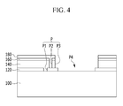
- FIG. 4 is a cross-sectional view taken along line IV-IV of FIG. 3
- FIG. 5 and FIG. 6 are schematic layout views showing a flow of current in first electrode and second electrode of the solar cell shown in FIG. 3 .
- the third separation groove P4 of FIG. 3 and FIG. 4 is connected to the second separation groove P3 by traversing the first separation groove P1 and the through groove P2 of any one of the separation groups P, and is connected to the second separation groove P3 of the separation group P adjacent thereto.
- the third separation groove P4 is located between two adjacent second separation grooves P3 and is connected to the two second separation grooves P3.
- each of the power generating parts includes the plurality of second electrodes 180 which are divided by the single first electrode 120 and the plurality of third separation grooves P4 as shown in FIG. 3 and FIG. 5 .
- the third separation grooves P4 that are located between adjacent second separation grooves P3 are offset from each other. Therefore, since the third separation grooves P4 continuous in an X-axis direction are not oriented or located on the same line (i.e., they are not collinear), the third separation grooves P4 adjacent to one another in the X-axis direction are not connected to each other.
- the third separation groove P4 When forming the third separation groove P4 according to the this embodiment, it is possible to minimize the degradation in generating efficiency even if the second separation groove P3 and through groove P2 are not separated from each other, such that a short-circuit is generated in the portion which is not separated.
- FIG. 6 shows a case in which a portion of the second electrode of the adjacent power generating part is short-circuited BB.
- Each of the power generating parts according to the related art includes a single second electrode. Accordingly, the whole second electrode of the two power generating parts adjacent to each other may be short-circuited even though a defect is generated in only a portion rather than the whole second separation groove P3, such that a leakage current is generated in the whole second electrode forming the single power generating part. As a result, the current loss may be greater.
- the single power generating part includes the plurality of second electrodes. Therefore, even if a portion of the second separation groove P3 is defective, only the portion of the second electrode positioned at the portion that is defective is short-circuited. Therefore, an area of the second electrode to be short-circuited is decreased compared to in the related art where the entire second electrode forming the single power generating part may be short-circuited. As a result, the leakage current caused by the short-circuit in a power generating part according to an embodiment of the present invention is reduced. The leakage current may have an effect on the generating efficiency, but in such an embodiment, it is possible to minimize an influence of the leakage current from the generating efficiency by minimizing the leakage current.
- FIG. 7 is a layout view of a solar cell according to another embodiment
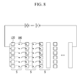
- FIG. 8 and FIG. 9 are schematic layout views showing a flow of current in first electrode and second electrode of the solar cell shown in FIG. 7 .
- the third separation groove P4 is connected to the first separation groove P1 by traversing the through groove P2 and the second separation groove P3 of any one of the separation groups P, and is connected to the first separation groove P1 of the separation group P adjacent thereto.
- the third separation groove P4 is located between the two first separation grooves P3 adjacent to each other and is connected to the two first separation grooves P1.
- each of the power generating parts includes the plurality of first electrodes 120 and the single second electrode 170 which are divided by the plurality of third separation grooves P4 as shown in FIG. 7 and FIG. 8 .
- the third separation grooves P4 that are located at both sides based on the first separation groove P1 are offset from each other. Therefore, since the third separation grooves P4 oriented in the X-axis direction are not located on the same line, the third separation grooves P4 adjacent in the X-axis direction are not connected to each other.
- the third separation groove P4 When forming the third separation groove P4 according to this embodiment, it is possible to minimize the degradation in generating efficiency even if the first separation groove P1 and through groove P2 are not separated from each other, such that a short-circuit is generated in the portion which is not separated.
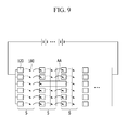
- FIG. 9 shows a case in which a portion of the first electrode of the adjacent power generating part is short-circuited AA.
- each of the power generating parts includes a single first electrode, wherein the whole first electrode of the two power generating parts adjacent to each other is short-circuited even though a defect may be generated in only a portion rather than the whole second separation groove P3 adjacent thereto, such that a leakage current is generated in the whole first electrode forming the single power generating part.
- the current loss may be greater.
- the single power generating part includes a plurality of first electrodes. Therefore, even though the portion of the first separation groove P3 is defective, only the portion of the first electrode positioned at the portion that is defective is short-circuited. Therefore, an area of the first electrode to be short-circuited is decreased compared to in the related art where the whole first electrode forming the single power generating part may be short-circuited. As a result, the leakage current caused by the short-circuit is reduced.
- the leakage current may have an effect on the generating efficiency, but in the exemplary embodiment, it is possible to minimize an influence of the leakage current from the generating efficiency by minimizing the leakage current.
- first electrode and second electrode may be divided as shown in FIG. 10 to FIG. 15 .
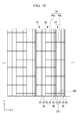
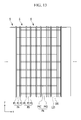
- FIG. 10 is a layout view of a solar cell according to another embodiment of the invention
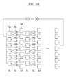
- FIG. 11 is a schematic layout view showing a power generating part forming the solar cell of FIG. 10
- FIG. 12 is schematic layout view showing a flow of current in first electrode and second electrode of the solar cell shown in FIG. 10 .
- the third separating groove P4 traverses two second electrodes 180 adjacent to each other in the X-axis direction and the third separating grooves P4 adjacent to each other in a Y-axis direction are offset from each other by the width of the second electrode. Therefore, the third separating groove P4 traverses any one of separation groups and is connected to the second separation groove P3 of the separation groups that are located at both sides based on the traversing single separation group.
- the third separating groove P4 includes the first horizontal part P4A traversing the first separation group PA of the continuous first separation group PA, second separation group PB and third separation group PC among the separation groups and connected to the second separation groove P3 of the second separation group PB, and the second horizontal part P4B traversing the second separation group PB and connected to the second separation groove P3 of the first separation group PA and third separation group PC.
- the first power generating part S1 is divided by the first horizontal parts P4A disposed at predetermined intervals
- the second power generating part S2 is divided by the first horizontal parts P4A and second horizontal parts P4B alternately disposed at predetermined intervals
- the third power generating part S3 is divided by the second horizontal parts P4B disposed at predetermined intervals, among the power generating parts that are separated by the first to third separation groups.
- the first horizontal parts P4A and second horizontal parts P4B are formed so as to traverse the two power generating parts, the first horizontal parts P4A and second horizontal parts P4B are offset from each other by the width of the second electrode 180. Therefore, each of the first horizontal parts P4A and second horizontal parts P4B oriented in the X-axis direction are located on the same line, but the first horizontal part P4A and second horizontal part P4B are not located on the same line, such that the third separation grooves P4 adjacent in the X-axis direction are not connected to each other.
- both of the first electrode 120 and second electrode 180 are divided, such that each of the power generating parts is divided into a plurality of small power generating parts as shown in FIG. 11 .
- the first electrode 120 and second electrode 180 may have a shape and a size changed according to the positions of the first horizontal part P4A and second horizontal part P4B, when the first electrode 120 and second electrode 180 are formed as shown in FIG. 10 , the first power generating part S1 and the third power generating part S3 are divided into a plurality of first small power generating parts SA, and the second power generating part S2 is divided into a second small power generating part SB having a smaller size than the first small power generating part SA as shown in FIG. 11 .
- FIG. 10 shows a case in which the third separation grooves P4 traverse two power generating parts among the continuous three power generating parts S1 to S3 and have the first horizontal part P4A and second horizontal part P4B, wherein the first and second horizontal parts arranged in the Y-axis direction along the separation group are offset from each other by the width of the second electrode.
- each of the third separation grooves includes a third horizontal part connected to the second separation groove of two adjacent separation groups, and a fourth horizontal part connected to the first separation groove of the two separation groups.
- the third separation grooves P4 may be formed with respect to the four or more continuous power generation parts, and the three third separation grooves P4 continuous in the X-axis direction are colinear.
- the horizontal parts adjacent to one another in the Y-axis direction along the separation groups may be offset from one another.
- the third separation groove P4 is formed so as to have the first horizontal part and second horizontal part, it is possible to minimize the degradation in generating efficiency even if a portion of the first separation groove P1 or the second separation groove P3 is defective to short-circuit the first electrode or second electrode adjacent thereto.
- the first electrode or second electrode connected to the portion that is short-circuited BB is made to have the area smaller than the first electrode or second electrode that is formed on the whole power generating part, such that the leakage current may be reduced, as compared to the related art. Therefore, it is possible to minimize an influence of the leakage current on the generating efficiency.
- FIG. 13 is a layout view of a solar cell according to another embodiment of the invention
- FIG. 14 is schematic layout view showing a flow of current in first electrode and second electrode of the solar cell shown in FIG. 13
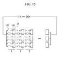
- FIG. 15 is schematic layout view showing a flow of current in first electrode and second electrode of a solar cell according to another embodiment.
- the third separation groove P4 includes a third horizontal part P4C that connects the first separation groove P1 of the two separate groups PA and PB adjacent to each other and a fourth horizontal part P4D that connects the second separation groove P3 thereof, and the third horizontal part P4C and fourth horizontal part P4D are repeatedly located at predetermined intervals in the Y-axis direction along the separation group.
- the third horizontal part P4C and fourth horizontal part P4D of the third separation groove P4 are offset from each other in the Y-axis direction, and the third horizontal parts P4C and fourth horizontal parts P4D oriented in the X-axis direction are located on the same line.
- the single power generating part S includes the plurality of small power generating parts SS, and each of the small power generating parts SS includes the single first electrode 120 and the two second electrodes 180.
- each of the small power generating parts SS may include the two first electrodes 120 and the signal second electrode 180.
- the first electrode 120 and the second electrode 180 are divided so that the single power generating part includes the plurality of small power generating parts, such that it is possible to minimize an amount of the leakage current generated due to the short-circuit even though the first electrode 120 or the second electrode 180 is short-circuited.
Landscapes
- Photovoltaic Devices (AREA)
Abstract
Disclosed herein is a solar cell, the solar cell includes a substrate, a plurality of first electrodes formed on the substrate and separated into a plurality of first separation grooves, a buffer layer and an optical active layer formed on the first electrode and having a through groove exposing the first electrode adjacent thereto, and a plurality of second electrodes formed on the optical active layer, separated into a plurality of second separation grooves, and electrically connected to the first electrode through the through groove, wherein the first electrode or the second electrode is divided by a plurality of third separation groove formed in a direction intersecting with the first separation groove, the through groove, and the second separation groove.
Description
- The present invention relates generally to a solar cell.
- A solar cell, which is a photovoltaic device that converts solar energy into electrical energy, is a next-generation pollution free energy source.
- A solar cell typically includes p-type semiconductor and n-type semiconductor. When solar energy is absorbed at an optical active layer, an electron-hole pair (EHP) is generated in the semiconductor, wherein the generated electron and hole move to the n-type semiconductor and the p-type semiconductor, respectively, and are collected by electrodes, electrical energy can be generated.
- As the optical active layer, a compound semiconductor containing group I-III-VI elements may be used. The compound semiconductor may provide a high efficiency solar cell with a high light absorption coefficient and high optical stability.
- Some solar cells are made of unit cells of the same size which are electrically connected to each other on a substrate, and the unit cells may be separated through a scribing process and a patterning process such as laser irradiation after forming in a thin film over the entire surface of the substrate.
- In order to form the solar cell, a first patterning process of separating a lower electrode, a second patterning process of separating the optical active layer and a third patterning process of separating an upper electrode are performed. In this case, a length of the thin film separating at the time patterning process as a size of the substrate is increased, and it is difficult to adjust a constant depth of a separation groove, such that a pattern defect may occur. Accordingly, the efficiency of the solar cell may be degraded if the pattern is defective.
- The above information disclosed in this Background section is only for enhancement of understanding of the background of the described technology and therefore it may contain information that does not form the prior art that is already known in this country to a person of ordinary skill in the art.
- The present invention has been made to solve the above problem and to provide a solar cell capable of minimizing the efficiency loss due to an error in pattern even if a size of solar cell is increased.
- An embodiment of the invention provides a solar cell including: a substrate; a plurality of first electrodes formed on the substrate and separated into a plurality of first separation grooves; a buffer layer and an optical active layer formed on the first electrode and having a through groove exposing the first electrode adjacent thereto; and a plurality of second electrodes formed on the optical active layer, separated into a plurality of second separation grooves, and electrically connected to the first electrode through the through groove, wherein the first electrode or the second electrode is divided by a plurality of third separation groove formed in a direction intersecting with the first separation groove, the through groove, and the second separation groove.
- The first separation groove, the through groove, and the second separation groove may be disposed in the order of the first separation groove, the through groove, and the second separation groove to form one of separation group, and the separation group may be repeatedly disposed at predetermined interval.
- The third separation groove may be connected to the second separation groove adjacent thereto.
- The third separation grooves disposed at both sides, having the second separation groove disposed therebetween may be disposed to be shifted from each other.
- Each of the first electrode, optical active layer, buffer layer and second electrode divided by the separation group forms the power generating part, and each of the second electrodes of the power generating part may be divided in plural by the third separation groove.
- The third separation groove may be connected to the first separation grove adjacent thereto.
- The third separation grooves disposed at both sides, having the first separation groove disposed therebetween may be disposed to be shifted from each other.
- Each of the first electrode, optical active layer, buffer layer and second electrode divided by the separation group forms the power generating part, and each of the first electrodes of the power generating part may be divided in plural by the third separation groove.
- A width of the third separation groove may be 10µm to 30µm.
- Another embodiment provides a solar cell including: a substrate; a plurality of first electrodes formed on the substrate and separated into a plurality of first separation grooves; a buffer layer and an optical active layer formed on the first electrode and having a through groove exposing the first electrode adjacent thereto; and a plurality of second electrodes formed on the optical active layer, separated into a plurality of second separation grooves, and electrically connected to the first electrode through the through groove, the first electrode and the second electrode are divided by a plurality of third separation groove formed in a direction intersecting with the first separation groove, the through groove, and the second separation groove.
- The first separation groove, the through groove, and the second separation groove may be disposed in the order of the first separation groove, the through groove, and the second separation groove to form one of separation group, and the separation group may be repeatedly disposed at predetermined interval.
- The third separation groove may traverse any one of the separation groups and may be connected to the second separation groove of the separation groups that are disposed at both sides based on the traversing separation group.
- The third separation groove may include a first horizontal part traversing the first separation group of the continuous first, second and third separation groups among the separation groups and connected to the second separation groove of the second separation group, and a second horizontal part traversing the second separation group and connected to the second separation groove of the first and third separation groups.
- The first horizontal part and second horizontal part are alternately disposed along the separation groups and may be disposed to be alternated with each other.
- The third separation groove may include a third horizontal part connected to the second separation groove of the two separation groups adjacent to each other, and a fourth horizontal part connected to the first separation groove of the two separation groups.
- The third horizontal part and fourth horizontal part are alternately disposed along the separation groups and may be disposed to be alternated with each other.
- The third horizontal part disposed at both sides, having the second separation groove disposed therebetween may be disposed on the same line, and the fourth horizontal part disposed at both sides, having the first separation groove disposed therebetween may be disposed on the same line.
- Each of the first electrode, optical active layer, buffer layer and second electrode divided by the separation group forms the power generating part, and the power generating part may include a plurality of small power generating part divided by the third separation groove.
- At least one of the first electrode and the second electrode may be formed of a plurality of small electrode divided in the same size.
- A width of the third separation groove may be 10µm to 30µm.
- According to an embodiment of the invention, a solar cell can therefore minimize efficiency loss, even though the pattern is defective.
- At least some of the above and other features of the invention are set out in the claims.
-
-
FIG. 1 is a schematic layout view of a solar cell according to an embodiment of the invention. -
FIG. 2 is a cross-sectional view taken along line II-II ofFIG. 1 . -
FIG. 3 is a schematic layout view of a solar cell according to an embodiment of the invention. -
FIG. 4 is a cross-sectional view taken along line IV-IV ofFIG. 3 . -
FIG. 5 andFIG. 6 are schematic layout views showing a flow of current in first electrode and second electrode of the solar cell shown inFIG. 3 . -
FIG. 7 is a layout view of a solar cell according to another embodiment of the invention. -
FIG. 8 andFIG. 9 are schematic layout views showing a flow of current in first electrode and second electrode of the solar cell shown inFIG. 7 . -
FIG. 10 is a layout view of a solar cell according to another embodiment of the invention. -
FIG. 11 is a schematic layout view showing a power generating part forming the solar cell ofFIG. 10 . -
FIG. 12 is schematic layout view showing a flow of current in first electrode and second electrode of the solar cell shown inFIG. 10 . -
FIG. 13 is a layout view of a solar cell according to another embodiment of the invention. -
FIG. 14 is schematic layout view showing a flow of current in first electrode and second electrode of the solar cell shown inFIG. 13 . -
FIG. 15 is schematic layout view showing a flow of current in first electrode and second electrode of a solar cell according to another embodiment of the invention. - Hereinafter, embodiments of the inventions will be described in detail with reference to the accompanying drawings. However, the present invention may be modified in various different ways and is not limited to the embodiments provided in the present description.
- In the drawings, the thickness of layers, films, panels, regions, etc., are exaggerated for clarity. Like reference numerals designate like elements throughout the specification. It will be understood that when an element such as a layer, film, region, or substrate is referred to as being "on" another element, it can be directly on the other element or intervening elements may also be present. In contrast, when an element is referred to as being "directly on" another element, there are no intervening elements present.
- Hereinafter, a solar cell will be described in detail with reference to the accompanying drawings.
-
FIG. 1 is a schematic layout view of a solar cell according to an embodiment of the invention andFIG. 2 is a cross-sectional view taken along line II-II ofFIG. 1 . - As shown in
FIG. 1 andFIG. 2 , asubstrate 100 of a solar cell according to thisembodiment is provided with a plurality offirst electrodes 120 formed thereon. Thefirst electrodes 120 are separated into portions by first separation grooves P1 that are formed at regular intervals. In this embodiment, a width of the first separation groove may be from about 20µm to 100µm. - The
substrate 100 may be a transparent insulating glass substrate such as a soda-lime glass. - In this embodiment, the
first electrode 120 is formed from a metal having an excellent electric conductivity and being between the substrate and a material forming an opticalactive layer 140. Further, thefirst electrode 120 may be heat-resistant and provide an excellent interface bonding between the first electrode and thesubstrate 100. For example, thefirst electrode 120 may be made from molybdenum (Mo). - The optical
active layer 140 and abuffer layer 160 are formed on thefirst electrode 120. The opticalactive layer 140 and thebuffer layer 160 are in contact with the substrate while covering the first separation groove P1. - The optical
active layer 140, which is a copper indium selenide (CIS)-based semiconductor of a P type, may contain selenium (Se) or sulfur (S). For example, as I-III-VI based semiconductor compound, the opticalactive layer 140 may be Cu(In1-x,Gax)(Se1-x,Sx) and a compound semiconductor having a composition of 0≤x≤1. The opticalactive layer 140 may be a single phase such that a composition in the compound semiconductor is substantially uniform. For example, the opticalactive layer 140 may be made from CuInSe2, CuInS2, Cu(In,Ga)Se2, (Ag,Cu)(In,Ga)Se2, (Ag,Cu)(In,Ga)(Se,S)2, Cu(In,Ga)(Se,S)2 or Cu(In,Ga)S2. - The optical
active layer 140 may include sodium (Na), which is diffused from thesubstrate 100. - The
buffer layer 160, which is an n-type semiconductor material having a high light transmittance, serves to alleviate the energy-gap difference between the opticalactive layer 140 and thesecond electrode 180. Thebuffer layer 160, which is the n-type semiconductor material having the high light transmittance, for example, may be formed of cadmium (CdS), zinc sulfide (ZnS) or zinc indium (Ins). - The
buffer layer 160 and the opticalactive layer 140 include a through groove P2 exposing thefirst electrode 120. In this embodiment, the through groove P2 exposes thefirst electrode 120 adjacent thereto. The through groove P2 is line-shaped and extends alongside the first separation groove P1, and a width thereof may be from about 20µm to 100µm. - The
second electrode 180 divided by the second separation groove P3 is formed on thebuffer layer 160. - The
second electrode 180 may be made of a material, for example, indium tin oxide(ITO), indium zinc oxide(IZO) and zinc oxide (Zno) having high light transmittance and the excellent electric conductivity and may be formed of a single layer or a multi-layer. The light transmittance of thesecond electrode 180 may be 80% or more. Further, in this embodiment, the ZnO layer is doped with a conductivity-type impurity such as aluminum (Al) or boron (B), such that it has low resistance value. - When the
second electrode 180 is formed as a multi-layer structure, the ITO layer having an excellent electro-optical characteristic may be stacked on the ZnO layer, or a n-type ZnO layer that is doped with a conductivity impurity to have low resistance may be stacked on an i-type ZnO layer that is not doped with the conductivity impurity. - The
second electrode 180, which is the n-type semiconductor, forms a pn junction with the opticalactive layer 140 which is the p-type semiconductor. - Each of the
second electrodes 180 is electrically connected by contacting thefirst electrode 120 adjacent thereto through the through groove P2. - The second separation groove P3 dividing the
second electrode 180 and exposing thefirst electrode 120 is line-shape and extends alongside the first separation groove P1, and a width of the second separation groove P3 may be about 20µm to 100µm. - The first separation groove P1, the through groove P2, and the second separation groove P3 traverse the substrate and are disposed in the order of the first separation groove P1, the through groove P2, and the second separation groove P3 to provide for one separation group which is spaced from other groups. The solar cell includes a power generating part (S) divided by the separation group.
- Each of the power generating parts (S) includes the
first electrode 120, the opticalactive layer 140, thebuffer layer 160, and thesecond electrode 180, and thefirst electrode 120 andsecond electrode 180 of the two power generating parts adjacent to each other are electrically connected to each other through the through groove P2. - In this embodiment, each of the power generating parts is divided by a plurality of third separation grooves P4 which are formed on the second electrode, the buffer layer, the optical active layer, and the first electrode to expose the substrate. A width of the third separation groove P4 may be 30µm or less, or in one embodiment, between about 10µm to about 30µm.
- The plurality of third separation grooves P4 may be formed in various orientations that are described in detail with reference to
FIG. 3 to FIG. 13 . -
FIG. 3 is a schematic layout view of a solar cell according to an embodiment of the invention,FIG. 4 is a cross-sectional view taken along line IV-IV ofFIG. 3 , andFIG. 5 andFIG. 6 are schematic layout views showing a flow of current in first electrode and second electrode of the solar cell shown inFIG. 3 . - The third separation groove P4 of
FIG. 3 andFIG. 4 is connected to the second separation groove P3 by traversing the first separation groove P1 and the through groove P2 of any one of the separation groups P, and is connected to the second separation groove P3 of the separation group P adjacent thereto. In other words, the third separation groove P4 is located between two adjacent second separation grooves P3 and is connected to the two second separation grooves P3. - Accordingly, each of the power generating parts includes the plurality of
second electrodes 180 which are divided by the singlefirst electrode 120 and the plurality of third separation grooves P4 as shown inFIG. 3 andFIG. 5 . - With continued reference to
FIG. 3 , the third separation grooves P4 that are located between adjacent second separation grooves P3 are offset from each other. Therefore, since the third separation grooves P4 continuous in an X-axis direction are not oriented or located on the same line (i.e., they are not collinear), the third separation grooves P4 adjacent to one another in the X-axis direction are not connected to each other. - When forming the third separation groove P4 according to the this embodiment, it is possible to minimize the degradation in generating efficiency even if the second separation groove P3 and through groove P2 are not separated from each other, such that a short-circuit is generated in the portion which is not separated.
- This will be described below with reference to
FIG. 6 . -
FIG. 6 shows a case in which a portion of the second electrode of the adjacent power generating part is short-circuited BB. - Each of the power generating parts according to the related art includes a single second electrode. Accordingly, the whole second electrode of the two power generating parts adjacent to each other may be short-circuited even though a defect is generated in only a portion rather than the whole second separation groove P3, such that a leakage current is generated in the whole second electrode forming the single power generating part. As a result, the current loss may be greater.
- However, when forming a third separation groove P4 according to an embodiment of the invention the single power generating part includes the plurality of second electrodes. Therefore, even if a portion of the second separation groove P3 is defective, only the portion of the second electrode positioned at the portion that is defective is short-circuited. Therefore, an area of the second electrode to be short-circuited is decreased compared to in the related art where the entire second electrode forming the single power generating part may be short-circuited. As a result, the leakage current caused by the short-circuit in a power generating part according to an embodiment of the present invention is reduced. The leakage current may have an effect on the generating efficiency, but in such an embodiment, it is possible to minimize an influence of the leakage current from the generating efficiency by minimizing the leakage current.
-
FIG. 7 is a layout view of a solar cell according to another embodiment, andFIG. 8 andFIG. 9 are schematic layout views showing a flow of current in first electrode and second electrode of the solar cell shown inFIG. 7 . - As shown in
FIG. 7 , the third separation groove P4 is connected to the first separation groove P1 by traversing the through groove P2 and the second separation groove P3 of any one of the separation groups P, and is connected to the first separation groove P1 of the separation group P adjacent thereto. In other words, the third separation groove P4 is located between the two first separation grooves P3 adjacent to each other and is connected to the two first separation grooves P1. - Therefore, each of the power generating parts includes the plurality of
first electrodes 120 and the single second electrode 170 which are divided by the plurality of third separation grooves P4 as shown inFIG. 7 andFIG. 8 . - Again, referring to
FIG. 7 , the third separation grooves P4 that are located at both sides based on the first separation groove P1 are offset from each other. Therefore, since the third separation grooves P4 oriented in the X-axis direction are not located on the same line, the third separation grooves P4 adjacent in the X-axis direction are not connected to each other. - When forming the third separation groove P4 according to this embodiment, it is possible to minimize the degradation in generating efficiency even if the first separation groove P1 and through groove P2 are not separated from each other, such that a short-circuit is generated in the portion which is not separated.
- This will be described below with reference to
FIG. 9 . -
FIG. 9 shows a case in which a portion of the first electrode of the adjacent power generating part is short-circuited AA. - According to some related-art products, each of the power generating parts includes a single first electrode, wherein the whole first electrode of the two power generating parts adjacent to each other is short-circuited even though a defect may be generated in only a portion rather than the whole second separation groove P3 adjacent thereto, such that a leakage current is generated in the whole first electrode forming the single power generating part. As a result, the current loss may be greater.
- However, when forming the third separation groove P4 according to this embodiment, the single power generating part includes a plurality of first electrodes. Therefore, even though the portion of the first separation groove P3 is defective, only the portion of the first electrode positioned at the portion that is defective is short-circuited. Therefore, an area of the first electrode to be short-circuited is decreased compared to in the related art where the whole first electrode forming the single power generating part may be short-circuited. As a result, the leakage current caused by the short-circuit is reduced. The leakage current may have an effect on the generating efficiency, but in the exemplary embodiment, it is possible to minimize an influence of the leakage current from the generating efficiency by minimizing the leakage current.
- Although this embodiment has been described with reference to the case in which the first electrode or second electrode is divided in plural, the first electrode and second electrode may be divided as shown in
FIG. 10 to FIG. 15 . -
FIG. 10 is a layout view of a solar cell according to another embodiment of the invention,FIG. 11 is a schematic layout view showing a power generating part forming the solar cell ofFIG. 10 , andFIG. 12 is schematic layout view showing a flow of current in first electrode and second electrode of the solar cell shown inFIG. 10 . - As shown in
Fig. 10 , the third separating groove P4 traverses twosecond electrodes 180 adjacent to each other in the X-axis direction and the third separating grooves P4 adjacent to each other in a Y-axis direction are offset from each other by the width of the second electrode. Therefore, the third separating groove P4 traverses any one of separation groups and is connected to the second separation groove P3 of the separation groups that are located at both sides based on the traversing single separation group. - The third separating groove P4 includes the first horizontal part P4A traversing the first separation group PA of the continuous first separation group PA, second separation group PB and third separation group PC among the separation groups and connected to the second separation groove P3 of the second separation group PB, and the second horizontal part P4B traversing the second separation group PB and connected to the second separation groove P3 of the first separation group PA and third separation group PC.
- Therefore, the first power generating part S1 is divided by the first horizontal parts P4A disposed at predetermined intervals, the second power generating part S2 is divided by the first horizontal parts P4A and second horizontal parts P4B alternately disposed at predetermined intervals, and the third power generating part S3 is divided by the second horizontal parts P4B disposed at predetermined intervals, among the power generating parts that are separated by the first to third separation groups.
- Among the power generating parts divided by the three separation groups, when the first horizontal parts P4A and second horizontal parts P4B are formed so as to traverse the two power generating parts, the first horizontal parts P4A and second horizontal parts P4B are offset from each other by the width of the
second electrode 180. Therefore, each of the first horizontal parts P4A and second horizontal parts P4B oriented in the X-axis direction are located on the same line, but the first horizontal part P4A and second horizontal part P4B are not located on the same line, such that the third separation grooves P4 adjacent in the X-axis direction are not connected to each other. - As shown in
FIG. 10 , when the third separation grooves P4 having the first horizontal part P4A and second horizontal part P4B are formed, both of thefirst electrode 120 andsecond electrode 180 are divided, such that each of the power generating parts is divided into a plurality of small power generating parts as shown inFIG. 11 . - In this embodiment, the
first electrode 120 andsecond electrode 180 may have a shape and a size changed according to the positions of the first horizontal part P4A and second horizontal part P4B, when thefirst electrode 120 andsecond electrode 180 are formed as shown inFIG. 10 , the first power generating part S1 and the third power generating part S3 are divided into a plurality of first small power generating parts SA, and the second power generating part S2 is divided into a second small power generating part SB having a smaller size than the first small power generating part SA as shown inFIG. 11 . -
FIG. 10 shows a case in which the third separation grooves P4 traverse two power generating parts among the continuous three power generating parts S1 to S3 and have the first horizontal part P4A and second horizontal part P4B, wherein the first and second horizontal parts arranged in the Y-axis direction along the separation group are offset from each other by the width of the second electrode. In other words, each of the third separation grooves includes a third horizontal part connected to the second separation groove of two adjacent separation groups, and a fourth horizontal part connected to the first separation groove of the two separation groups. Further, the third separation grooves P4 may be formed with respect to the four or more continuous power generation parts, and the three third separation grooves P4 continuous in the X-axis direction are colinear. In this embodiment, so as not to be connected to each other, the horizontal parts adjacent to one another in the Y-axis direction along the separation groups may be offset from one another. - As shown in
FIG. 10 , when the third separation groove P4 is formed so as to have the first horizontal part and second horizontal part, it is possible to minimize the degradation in generating efficiency even if a portion of the first separation groove P1 or the second separation groove P3 is defective to short-circuit the first electrode or second electrode adjacent thereto. - In other words, as shown in
FIG. 12 , even though thefirst electrode 120 or thesecond electrode 180 is short-circuited, the first electrode or second electrode connected to the portion that is short-circuited BB is made to have the area smaller than the first electrode or second electrode that is formed on the whole power generating part, such that the leakage current may be reduced, as compared to the related art. Therefore, it is possible to minimize an influence of the leakage current on the generating efficiency. -
FIG. 13 is a layout view of a solar cell according to another embodiment of the invention,FIG. 14 is schematic layout view showing a flow of current in first electrode and second electrode of the solar cell shown inFIG. 13 , andFIG. 15 is schematic layout view showing a flow of current in first electrode and second electrode of a solar cell according to another embodiment. - As shown in
FIG. 13 , the third separation groove P4 includes a third horizontal part P4C that connects the first separation groove P1 of the two separate groups PA and PB adjacent to each other and a fourth horizontal part P4D that connects the second separation groove P3 thereof, and the third horizontal part P4C and fourth horizontal part P4D are repeatedly located at predetermined intervals in the Y-axis direction along the separation group. - The third horizontal part P4C and fourth horizontal part P4D of the third separation groove P4 are offset from each other in the Y-axis direction, and the third horizontal parts P4C and fourth horizontal parts P4D oriented in the X-axis direction are located on the same line.
- When the third separation groove P4 is formed so as to have the third horizontal part P4C and fourth horizontal part P4D, the plurality of
first electrodes 120 andsecond electrodes 180 are formed as shown inFIG. 14 . Therefore, the single power generating part S includes the plurality of small power generating parts SS, and each of the small power generating parts SS includes the singlefirst electrode 120 and the twosecond electrodes 180. On the other hand, as shown inFIG. 15 , each of the small power generating parts SS may include the twofirst electrodes 120 and the signalsecond electrode 180. - As shown in
FIG. 10 to FIG. 15 , when the third separation groove P4 is formed so as to have the plurality of horizontal parts that are offset from each other, thefirst electrode 120 and thesecond electrode 180 are divided so that the single power generating part includes the plurality of small power generating parts, such that it is possible to minimize an amount of the leakage current generated due to the short-circuit even though thefirst electrode 120 or thesecond electrode 180 is short-circuited. - While this disclosure has been described in connection with what is presently considered to be practical embodiment of the invention, it is to be understood that the invention is not limited to the disclosed embodiments, but, on the contrary, is intended to cover various modifications and equivalent arrangements included within the scope of the appended claims.
Claims (15)
- A solar cell comprising:a substrate;a plurality of first electrodes located on the substrate and separated by a plurality of first separation grooves extending in a first direction;a buffer layer and an optical active layer located on each of the first electrodes and having a through groove exposing a first one of the first electrodes;a plurality of second electrodes located on the optical active layer and separated from each other by one of a plurality of second separation grooves, one of the second electrodes being electrically connected to the first electrode via the through groove; anda plurality of third separation grooves, each extending in a second direction intersecting the first direction and extending between adjacent ones of the said second separation grooves.
- A solar cell according to claim 1, wherein the second separation grooves divide the buffer layer, the optical active layer, and the second electrodes into separation groups.
- A solar cell according to claim 1 or 2, wherein each of the third separation grooves is connected to adjacent ones of the second separation grooves.
- A solar cell according to claim 1 or 2, wherein each of the third separation grooves is connected to adjacent ones of the first separation grooves.
- A solar cell according to claim 3 or 4, wherein each of the third separation grooves is offset from an adjacent one of the third separation grooves in the first direction.
- A solar cell according to claim 5, wherein: each of separation groups forms a power generating part; and
adjacent ones of the second electrodes of each power generating part are separated by one of the third separation grooves. - A solar cell according to claim 6, wherein each power generating part comprises a plurality of smaller power generating parts defined by the third separation groove.
- A solar cell according to claim 7, wherein at least one of the first electrode and the second electrode comprises a plurality of small electrodes of the same size.
- A solar cell according to any preceding claim, wherein a width of each of the third separation grooves is from 10µm to 30µm.
- A solar cell according to claim 2 or any claim dependent upon claim 2, wherein each of the third separations grooves comprises:a first part traversing a first one of the separation groups and connected to the second separation groove of a second one of the separation groups adjacent to the first one of the separation groups; anda second part traversing the second one of the separation groups and connected to the second separation groove of the first one of the separation groups and the second separation groove of a third one of the separation groups.
- A solar cell according to claim 10, wherein the first parts and second parts are arranged alternately in the first direction.
- A solar cell according to claim 2 or one of claims 3 to 9 when dependent upon claim 2, wherein each of the third separation grooves traverses one of the separation groups and is connected to one of the second separation grooves of adjacent ones of the separation groups.
- A solar cell according to claim 12, wherein each of the third separation grooves includes a third part connected to the second separation groove of two adjacent separation groups, and a fourth part connected to the first separation groove of the two separation groups.
- A solar cell according toclaim 13, wherein the third part and fourth part are arranged alternately in the first direction.
- A solar cell according to claim 14, wherein each third part has adjacent ones of the second separation grooves located therebetween and is colinear with an adjacent third part, and wherein each fourth part has adjacent ones of the first separation grooves located therebetween and is colinear with an adjacent fourth part.
Applications Claiming Priority (1)
| Application Number | Priority Date | Filing Date | Title |
|---|---|---|---|
| KR1020130141705A KR20150057852A (en) | 2013-11-20 | 2013-11-20 | Solar cell |
Publications (1)
| Publication Number | Publication Date |
|---|---|
| EP2876695A1 true EP2876695A1 (en) | 2015-05-27 |
Family
ID=51903846
Family Applications (1)
| Application Number | Title | Priority Date | Filing Date |
|---|---|---|---|
| EP14193971.0A Withdrawn EP2876695A1 (en) | 2013-11-20 | 2014-11-20 | Solar cell |
Country Status (3)
| Country | Link |
|---|---|
| US (1) | US20150136203A1 (en) |
| EP (1) | EP2876695A1 (en) |
| KR (1) | KR20150057852A (en) |
Families Citing this family (1)
| Publication number | Priority date | Publication date | Assignee | Title |
|---|---|---|---|---|
| DE102019129355A1 (en) * | 2019-10-30 | 2021-05-06 | Heliatek Gmbh | Photovoltaic element with improved efficiency in the case of shading and method for producing such a photovoltaic element |
Citations (3)
| Publication number | Priority date | Publication date | Assignee | Title |
|---|---|---|---|---|
| EP2383783A2 (en) * | 2010-04-30 | 2011-11-02 | Axuntek Solar Energy | See-through solar battery module and manufacturing method thereof |
| EP2485273A2 (en) * | 2009-10-01 | 2012-08-08 | LG Innotek Co., Ltd. | Solar photovoltaic device and a production method for the same |
| US20130247969A1 (en) * | 2012-03-21 | 2013-09-26 | Dong-jin Kim | Solar cell and method of manufacturing the same |
Family Cites Families (1)
| Publication number | Priority date | Publication date | Assignee | Title |
|---|---|---|---|---|
| US20100236607A1 (en) * | 2008-06-12 | 2010-09-23 | General Electric Company | Monolithically integrated solar modules and methods of manufacture |
-
2013
- 2013-11-20 KR KR1020130141705A patent/KR20150057852A/en not_active Withdrawn
-
2014
- 2014-04-25 US US14/262,509 patent/US20150136203A1/en not_active Abandoned
- 2014-11-20 EP EP14193971.0A patent/EP2876695A1/en not_active Withdrawn
Patent Citations (3)
| Publication number | Priority date | Publication date | Assignee | Title |
|---|---|---|---|---|
| EP2485273A2 (en) * | 2009-10-01 | 2012-08-08 | LG Innotek Co., Ltd. | Solar photovoltaic device and a production method for the same |
| EP2383783A2 (en) * | 2010-04-30 | 2011-11-02 | Axuntek Solar Energy | See-through solar battery module and manufacturing method thereof |
| US20130247969A1 (en) * | 2012-03-21 | 2013-09-26 | Dong-jin Kim | Solar cell and method of manufacturing the same |
Also Published As
| Publication number | Publication date |
|---|---|
| US20150136203A1 (en) | 2015-05-21 |
| KR20150057852A (en) | 2015-05-28 |
Similar Documents
| Publication | Publication Date | Title |
|---|---|---|
| KR101210168B1 (en) | Solar cell apparatus and method of fabricating the same | |
| KR100999797B1 (en) | Photovoltaic device and its manufacturing method | |
| KR20130107115A (en) | Solar cell and manufacturing method thereof | |
| KR20150045309A (en) | Solar cell module | |
| EP2876693A1 (en) | Solar cell | |
| CN102714231A (en) | Solar cell array and thin-film solar module and production method therefor | |
| KR101114079B1 (en) | Solar cell apparatus and method of fabricating the same | |
| KR101349429B1 (en) | Photovoltaic apparatus | |
| KR101272997B1 (en) | Solar cell apparatus and method of fabricating the same | |
| US20150136203A1 (en) | Solar cell | |
| KR20130136739A (en) | Solar cell and method of fabricating the same | |
| KR20140143289A (en) | Photoelectric module and manufacturing method for the same | |
| KR20130070464A (en) | Solar cell apparatus and method of fabricating the same | |
| US20150136197A1 (en) | Solar cell array | |
| JP2016171186A (en) | Photoelectric conversion device | |
| KR101220015B1 (en) | Solar cell apparatus and method of fabricating the same | |
| KR101283302B1 (en) | Solar cell apparatus and method of fabricating the same | |
| KR101765922B1 (en) | Solar cell apparatus and method of fabricating the same | |
| US20150136223A1 (en) | Solar cell and method for manufacturing the same | |
| KR101762958B1 (en) | Solar cell apparatus and method of fabricating the same | |
| KR101306436B1 (en) | Solar cell apparatus and method of fabricating the same | |
| KR101349525B1 (en) | Photovoltaic apparatus | |
| KR101189366B1 (en) | Solar cell apparatus and method of fabricating the same | |
| KR101081222B1 (en) | Solar cell aparatus | |
| JP2015122389A (en) | Photoelectric conversion device |
Legal Events
| Date | Code | Title | Description |
|---|---|---|---|
| PUAI | Public reference made under article 153(3) epc to a published international application that has entered the european phase |
Free format text: ORIGINAL CODE: 0009012 |
|
| 17P | Request for examination filed |
Effective date: 20141120 |
|
| AK | Designated contracting states |
Kind code of ref document: A1 Designated state(s): AL AT BE BG CH CY CZ DE DK EE ES FI FR GB GR HR HU IE IS IT LI LT LU LV MC MK MT NL NO PL PT RO RS SE SI SK SM TR |
|
| AX | Request for extension of the european patent |
Extension state: BA ME |
|
| STAA | Information on the status of an ep patent application or granted ep patent |
Free format text: STATUS: THE APPLICATION IS DEEMED TO BE WITHDRAWN |
|
| 18D | Application deemed to be withdrawn |
Effective date: 20151128 |