EP2876678A1 - Heat dissipation device and semiconductor device - Google Patents
Heat dissipation device and semiconductor device Download PDFInfo
- Publication number
- EP2876678A1 EP2876678A1 EP13820186.8A EP13820186A EP2876678A1 EP 2876678 A1 EP2876678 A1 EP 2876678A1 EP 13820186 A EP13820186 A EP 13820186A EP 2876678 A1 EP2876678 A1 EP 2876678A1
- Authority
- EP
- European Patent Office
- Prior art keywords
- passage
- coolant
- hole
- heat dissipation
- dissipation device
- Prior art date
- Legal status (The legal status is an assumption and is not a legal conclusion. Google has not performed a legal analysis and makes no representation as to the accuracy of the status listed.)
- Withdrawn
Links
Images





Classifications
-
- H—ELECTRICITY
- H10—SEMICONDUCTOR DEVICES; ELECTRIC SOLID-STATE DEVICES NOT OTHERWISE PROVIDED FOR
- H10W—GENERIC PACKAGES, INTERCONNECTIONS, CONNECTORS OR OTHER CONSTRUCTIONAL DETAILS OF DEVICES COVERED BY CLASS H10
- H10W40/00—Arrangements for thermal protection or thermal control
- H10W40/40—Arrangements for thermal protection or thermal control involving heat exchange by flowing fluids
- H10W40/47—Arrangements for thermal protection or thermal control involving heat exchange by flowing fluids by flowing liquids, e.g. forced water cooling
-
- H—ELECTRICITY
- H10—SEMICONDUCTOR DEVICES; ELECTRIC SOLID-STATE DEVICES NOT OTHERWISE PROVIDED FOR
- H10W—GENERIC PACKAGES, INTERCONNECTIONS, CONNECTORS OR OTHER CONSTRUCTIONAL DETAILS OF DEVICES COVERED BY CLASS H10
- H10W40/00—Arrangements for thermal protection or thermal control
- H10W40/20—Arrangements for cooling
- H10W40/25—Arrangements for cooling characterised by their materials
- H10W40/255—Arrangements for cooling characterised by their materials having a laminate or multilayered structure, e.g. direct bond copper [DBC] ceramic substrates
-
- H—ELECTRICITY
- H10—SEMICONDUCTOR DEVICES; ELECTRIC SOLID-STATE DEVICES NOT OTHERWISE PROVIDED FOR
- H10W—GENERIC PACKAGES, INTERCONNECTIONS, CONNECTORS OR OTHER CONSTRUCTIONAL DETAILS OF DEVICES COVERED BY CLASS H10
- H10W40/00—Arrangements for thermal protection or thermal control
- H10W40/40—Arrangements for thermal protection or thermal control involving heat exchange by flowing fluids
- H10W40/43—Arrangements for thermal protection or thermal control involving heat exchange by flowing fluids by flowing gases, e.g. forced air cooling
-
- H—ELECTRICITY
- H10—SEMICONDUCTOR DEVICES; ELECTRIC SOLID-STATE DEVICES NOT OTHERWISE PROVIDED FOR
- H10W—GENERIC PACKAGES, INTERCONNECTIONS, CONNECTORS OR OTHER CONSTRUCTIONAL DETAILS OF DEVICES COVERED BY CLASS H10
- H10W72/00—Interconnections or connectors in packages
- H10W72/30—Die-attach connectors
-
- H—ELECTRICITY
- H10—SEMICONDUCTOR DEVICES; ELECTRIC SOLID-STATE DEVICES NOT OTHERWISE PROVIDED FOR
- H10W—GENERIC PACKAGES, INTERCONNECTIONS, CONNECTORS OR OTHER CONSTRUCTIONAL DETAILS OF DEVICES COVERED BY CLASS H10
- H10W40/00—Arrangements for thermal protection or thermal control
- H10W40/20—Arrangements for cooling
- H10W40/25—Arrangements for cooling characterised by their materials
- H10W40/259—Ceramics or glasses
-
- H—ELECTRICITY
- H10—SEMICONDUCTOR DEVICES; ELECTRIC SOLID-STATE DEVICES NOT OTHERWISE PROVIDED FOR
- H10W—GENERIC PACKAGES, INTERCONNECTIONS, CONNECTORS OR OTHER CONSTRUCTIONAL DETAILS OF DEVICES COVERED BY CLASS H10
- H10W72/00—Interconnections or connectors in packages
- H10W72/30—Die-attach connectors
- H10W72/351—Materials of die-attach connectors
- H10W72/352—Materials of die-attach connectors comprising metals or metalloids, e.g. solders
-
- H—ELECTRICITY
- H10—SEMICONDUCTOR DEVICES; ELECTRIC SOLID-STATE DEVICES NOT OTHERWISE PROVIDED FOR
- H10W—GENERIC PACKAGES, INTERCONNECTIONS, CONNECTORS OR OTHER CONSTRUCTIONAL DETAILS OF DEVICES COVERED BY CLASS H10
- H10W72/00—Interconnections or connectors in packages
- H10W72/90—Bond pads, in general
- H10W72/951—Materials of bond pads
- H10W72/952—Materials of bond pads comprising metals or metalloids, e.g. PbSn, Ag or Cu
-
- H—ELECTRICITY
- H10—SEMICONDUCTOR DEVICES; ELECTRIC SOLID-STATE DEVICES NOT OTHERWISE PROVIDED FOR
- H10W—GENERIC PACKAGES, INTERCONNECTIONS, CONNECTORS OR OTHER CONSTRUCTIONAL DETAILS OF DEVICES COVERED BY CLASS H10
- H10W90/00—Package configurations
- H10W90/701—Package configurations characterised by the relative positions of pads or connectors relative to package parts
- H10W90/731—Package configurations characterised by the relative positions of pads or connectors relative to package parts of die-attach connectors
- H10W90/734—Package configurations characterised by the relative positions of pads or connectors relative to package parts of die-attach connectors between a chip and a stacked insulating package substrate, interposer or RDL
Definitions
- the present invention relates to a heat dissipation device, formed by stacking ceramic sheets, and a semiconductor device, formed by mounting a metal plate to which a semiconductor element is coupled on a heat dissipation device.
- patent document 1 discloses this type of a heat dissipation device.
- the heat dissipation device of patent document 1 is formed by baking a lamination in which a plurality of ceramic sheets are stacked.
- the ceramic sheets include a ceramic sheet having a plurality of slits, which are elements of a coolant passage, and a ceramic sheet having a communication passage that communicates the coolant passage and the exterior.
- a metal plate to which a semiconductor element is coupled is joined with a heat dissipation device to form a semiconductor device. Heat is transmitted from the semiconductor element to the heat dissipation device through the metal plate and dissipated to the coolant flowing through the coolant passage. This cools the semiconductor element.
- Patent Document 1 International Publication No. WO2011/136362
- One aspect of a heat dissipation device of the present disclosure includes a base body formed by stacking a plurality of ceramic sheets, a coolant passage located in the base body and through which coolant flows, at least one mounting portion defined in a first surface of the base body as a location where a cooling subject is mounted, a slit formation layer formed by at least one of the ceramic sheets, and a communication passage formation layer formed by at least one of the ceramic sheets.
- the slit formation layer includes a plurality of slits that form a portion of the coolant passage. The slits are formed to be at least partially overlapped with a region that includes the mounting portion as viewed from a stacking direction of the ceramic sheets.
- the communication passage formation layer forms a portion of the coolant passage and includes a communication passage that communicates the slits.
- the slits are located toward the mounting portion from the communication passage in the stacking direction of the ceramic sheets.
- An overlapping portion of the slits and the communication passage is located proximate to a region where the mounting portion is located as viewed from the stacking direction.
- the heat dissipation device of the present disclosure includes a base body formed by stacking a plurality of ceramic members, a coolant passage located in the base body, and at least one mounting portion defined in a first surface of the base body as a location where a cooling subject is mounted.
- the coolant passage includes an underneath-lying passage that is formed underneath the mounting portion, a supply passage in communication with an upstream side of the underneath-lying passage in a direction coolant flows, a discharge passage in communication with a downstream side of the underneath-lying passage in the direction the coolant flows, and an expulsion passage located between the supply passage and the discharge passage.
- the supply passage supplies the coolant to the underneath-lying passage.
- the discharge passage discharges the coolant from the underneath-lying passage.
- the expulsion passage expels the coolant to the underneath-lying passage from a vertically lower side toward a vertically upper side.
- One aspect of a semiconductor device of the present disclosure includes the above heat dissipation device, a metal plate mounted on the mounting portion of the heat dissipation device, and a semiconductor element coupled to the metal plate.
- a semiconductor device 10 shown in Fig. 1 is formed by mounting a metal plate 13b to which a semiconductor element 13a is coupled and a metal plate 14b to which a semiconductor element 14a is coupled on one surface 12a (first surface) of a base body 12 of a heat dissipation device 11.
- the metal plates 13b and 14b which function as wiring layers and joining layers, are formed from pure aluminum (e.g., 1000 series aluminum, which is pure aluminum for industrial use) or copper.
- IGBTs insulated gate bipolar transistors
- the semiconductor elements 13a and 14a are joined with the metal plates 13b and 14b by performing metallic joining, for example, soldering or brazing.
- the metal plates 13b and 14b are joined with the heat dissipation device 11 by performing metallic joining, for example, soldering or brazing. In this manner, the metal plates 13b and 14b are mounted on the first surface 12a of the base body 12.
- first mounting portion 121 and a second mounting portion 131 which function as mounting portions on which the metal plates 13b and 14b are mounted. That is, a plurality of the mounting portions (two in the first embodiment) are arranged side by side on the first surface 12a of the base body 12.
- the base body 12 is formed by stacking a plurality of ceramic sheets (five sheets in the first embodiment). The base body 12 is baked to form the heat dissipation device 11.
- a ceramic material has high water resistance when water cooling is employed to cool the heat dissipation device 11.
- the heat dissipation device 11 of the first embodiment includes first to fifth ceramic sheets 21, 22, 23, 24, and 25 as elements serving as ceramic sheets.
- the first ceramic sheet 21 is located at the upper side
- the fifth ceramic sheet 25 is located at the lower side.
- the first ceramic sheet 21 forms a top plate portion of the heat dissipation device 11 and includes a surface (upper surface) defining the first surface 12a of the base body 12.
- a coolant supply hole 21 a and a coolant discharge hole 21 b extend through the first ceramic sheet 21.
- the coolant supply hole 21 a and the coolant discharge hole 21 b have the same open area.
- the coolant supply hole 21 a is connected to a supply pipe P1 (shown in Figs. 1 and 2 ) that supplies a coolant to the heat dissipation device 11.
- the coolant discharge hole 21 b is connected to a discharge pipe P2 (shown in Figs. 1 and 2 ) that discharges the coolant out of the heat dissipation device 11 to the exterior.
- a first coolant inlet hole 22a extends through the second ceramic sheet 22.
- the first coolant inlet hole 22a is located at a position where the first coolant inlet hole 22a is overlapped with the coolant supply hole 21 a as viewed from a stacking direction of the first to fifth ceramic sheets 21, 22, 23, 24, and 25.
- a first coolant outlet hole 22b extends through the second ceramic sheet 22.
- the first coolant outlet hole 22b is located at a position where the first coolant outlet hole 22b is overlapped with the coolant discharge hole 21 b as viewed from the stacking direction of the first to fifth ceramic sheets 21, 22, 23, 24, and 25 (hereafter, may be simply referred to as a stacking direction A).
- the first coolant inlet hole 22a and the first coolant outlet hole 22b are located in symmetric positions.
- the first coolant inlet hole 22a and the first coolant outlet hole 22b have the same open area.
- the second ceramic sheet 22 also includes a plurality of first slits 22c, which serve as slits, between the first coolant inlet hole 22a and the first coolant outlet hole 22b.
- Each first slit 22c extends through the second ceramic sheet 22 and extends straight in the second ceramic sheet 22 from a position that is closer to the first coolant inlet hole 22a toward a central portion of the second ceramic sheet 22.
- the first slits 22c have the same length.
- the first slits 22c have the same open area.
- the first slits 22c are at least partially located underneath the first mounting portion 121 (metal plate 13b and semiconductor element 13a). That is, the first slits 22c are at least partially overlapped with the first mounting portion 121 as viewed from the stacking direction A.
- the second ceramic sheet 22 also includes a plurality of second slits 22d, which serve as slits, between the first coolant inlet hole 22a and the first coolant outlet hole 22b.
- Each second slit 22d extends through the second ceramic sheet 22 and extends straight in the second ceramic sheet 22 from a position that is closer to the first coolant outlet hole 22b toward the central portion of the second ceramic sheet 22.
- the second slits 22d have the same length.
- the second slits 22d have the same open area.
- the second slits 22d are at least partially located underneath the second mounting portion 131 (metal plate 14b and semiconductor element 14a). That is, the second slits 22d are at least partially overlapped with the second mounting portion 131 as viewed from the stacking direction A.
- a second coolant inlet hole 23a extends through the third ceramic sheet 23.
- the second coolant inlet hole 23a is located in a position where the second coolant inlet hole 23a is overlapped with the first coolant inlet hole 22a as viewed from the stacking direction A.
- a second coolant outlet hole 23b extends through the third ceramic sheet 23.
- the second coolant outlet hole 23b is located in a position where the second coolant outlet hole 23b is overlapped with the first coolant outlet hole 22b as viewed from the stacking direction A.
- the second coolant inlet hole 23a and the second coolant outlet hole 23b have the same open area.
- the third ceramic sheet 23 also includes a first communication hole 23c, which extends in a direction orthogonal to the extending direction of each first slit 22c.
- the first communication hole 23c is partially overlapped with each first slit 22c at one end that is located toward the first coolant inlet hole 22a as viewed from the stacking direction A. This communicates each first slit 22c and the first communication hole 23c.
- the third ceramic sheet 23 includes a second communication hole 23d at a position closer to the second coolant outlet hole 23b than the first communication hole 23c.
- the second communication hole 23d extends in the direction orthogonal to the extending direction of each first slit 22c.
- the second communication hole 23d is partially overlapped with each first slit 22c at the other end, which is located toward the first coolant outlet hole 22b, as viewed from the stacking direction A. This communicates each first slit 22c and the second communication hole 23d.
- the third ceramic sheet 23 also includes a third communication hole 23e, which extends in a direction orthogonal to the extending direction of each second slit 22d.
- the third communication hole 23e is partially overlapped with each second slit 22d at one end that is located toward the first coolant inlet hole 22a as viewed from the stacking direction A. This communicates each second slit 22d and the third communication hole 23e.
- the third ceramic sheet 23 includes a fourth communication hole 23f at a position closer to the second coolant outlet hole 23b than the third communication hole 23e. The fourth communication hole 23f extends in the direction orthogonal to the extending direction of each second slit 22d.
- the fourth communication hole 23f is partially overlapped with each second slit 22d at the other end, which is located toward the first coolant outlet hole 22b, as viewed from the stacking direction A. This communicates each second slit 22d and the fourth communication hole 23f.
- the fourth ceramic sheet 24 includes a first through hole 24a, a second through hole 24b, and a third through hole 24c.
- the first through hole 24a is overlapped with the second coolant inlet hole 23a and a portion of the first communication hole 23c as viewed from the stacking direction A. This communicates the second coolant inlet hole 23a and the first communication hole 23c.
- the second through hole 24b is overlapped with a portion of the second communication hole 23d and a portion of the third communication hole 23e as viewed from the stacking direction A. This communicates the second communication hole 23d and the third communication hole 23e.
- the third communication hole 24c is overlapped with a portion of the fourth communication hole 23f and the second coolant outlet hole 23b as viewed from the stacking direction A.
- the fifth ceramic sheet 25 forms a bottom plate portion of the heat dissipation device 11 and includes a surface (lower surface) defining a second surface 12b of the base body 12. That is, the first surface 12a and the second surface 12b are located at opposite sides of the base body 12.
- the base body 12 of the heat dissipation device 11 is formed by sequentially stacking the fourth ceramic sheet 24, the third ceramic sheet 23, the second ceramic sheet 22, and the first ceramic sheet 21 on the fifth ceramic sheet 25.
- the interior of the base body 12 includes the coolant supply hole 21 a, the first coolant inlet hole 22a, the second coolant inlet hole 23a, the first through hole 24a, the first communication hole 23c, each first slit 22c, the second communication hole 23d, the second through hole 24b, the third communication hole 23e, each second slit 22d, the fourth communication hole 23f, the third through hole 24c, the second coolant outlet hole 23b, the first coolant outlet hole 22b, and the coolant discharge hole 21 b, which form a coolant passage 15 through which a coolant flows.
- the coolant supply hole 21 a and the coolant discharge hole 21 b open in the first surface 12a of the base body 12.
- the second communication hole 23d, the second through hole 24b, and the third communication hole 23e form a portion of the coolant passage 15 that is located between the first mounting portion 121 and the second mounting portion 131. That is, the second communication hole 23d, the second through hole 24b, and the third communication hole 23e form a portion of the coolant passage 15 that extends from the first mounting portion 121 toward the second surface 12b and extends from the second surface 12b toward the second mounting portion 131.
- the second ceramic sheet 22 corresponds to a slit formation layer that includes the first slits 22c and the second slits 22d, which form a portion of the coolant passage 15.
- the first communication hole 23c corresponds to a communication passage that is overlapped with each first slit 22c at a portion closer to the first coolant inlet hole 22a and communicates with each first slit 22c.
- the second communication hole 23d corresponds to a communication passage that is overlapped with each first slit 22c at a portion closer to the second coolant outlet hole 23b and communications with the first slits 22c.
- the third communication hole 23e corresponds to a communication passage that is overlapped with each second slit 22d at a portion closer to the first coolant inlet hole 22a and communicates with each second slit 22d.
- the fourth communication hole 23f corresponds to a communication passage that is overlapped with each second slit 22d at a portion closer to the first coolant outlet hole 22b and communicates with each second slit 22d.
- the third ceramic sheet 23 corresponds to a communication passage formation layer that includes the first communication hole 23c, the second communication hole 23d, the third communication hole 23e, and the fourth communication hole 23f, which correspond to the communication passages.
- the first slits 22c and the second slits 22d are located toward the first mounting portion 121 and the second mounting portion 131 from the first communication hole 23c, the second communication hole 23d, the third communication hole 23e, and the fourth communication hole 23f in the stacking direction A.
- the second communication hole 23d is continuous to the first slit 22c at a downstream side of the coolant flow
- the second through hole 24b is continuous to the second communication hole 23d.
- the extension passage W includes a passage surface X1 and a passage surface Y1 that are opposed in the stacking direction of the first to fifth ceramic sheets 21 to 25.
- the passage surface X1 is a portion of a passage formed by the first slit 22c, which is located closer to the first surface 12a of the base body 12.
- the passage surface Y1 is a portion of a passage formed by the second through hole 24b, which is located closer to the second surface 12b.
- the passage surface X1 is formed by a surface of the first ceramic sheet 21, which is located above the second ceramic sheet 22.
- the passage surface Y1 is formed by a surface of the fifth ceramic sheet 25, which is located below the fourth ceramic sheet 24. That is, a passage formed by the first slit 22c forms the coolant passage 15 that is located on the uppermost position in the stacking direction.
- the passage surface X1 corresponds to an upper surface of the passage.
- a passage formed by the second through hole 24b forms the coolant passage 15 that is located at the lowermost position in the stacking direction.
- the passage surface Y1 corresponds to a lower surface of the passage.
- a first fin 31 is located between adjacent ones of the first slits 22c.
- a second fin 32 is located between adjacent ones of the second slits 22d.
- the length H of the first fin 31 (length of the first slit 22c) is set to be within a region Z (dotted region in Fig. 6 ) as viewed from the stacking direction A.
- the region Z is located between straight lines A and B.
- the straight lines A and B extend from opposite ends 131 band 132b of the metal plate 13b at an angle ⁇ of 45° relative to the first surface 12a of the base body 12.
- the angle ⁇ of the straight lines A and B relative to the first surface 12a of the base body 12 only needs to be within 30° to 60°.
- the region Z which is located between the straight lines A and B, forms a heat transmission region where the heat generated by the semiconductor element 13a is transmitted to the heat dissipation device 11 through the metal plate 13b.
- a portion of the first communication hole 23c that corresponds to the region Z as viewed from the stacking direction A serves as an overlapping portion 35 of each first slit 22c and the first communication hole 23c.
- the overlapping portion 35 is located in the heat transmission region, where the heat generated by the semiconductor element 13a is transmitted to the heat dissipation device 11 through the metal plate 13b. That is, the overlapping portion 35 is located proximate to a region where the first mounting portion 121 is located as viewed from the stacking direction A.
- the overlapping portion 35 is located toward an inner side of the first slit 22c from one end 221c of each first slit 22c that is closer to the first coolant inlet hole 22a.
- the overlapping portion 35 includes a first overlapping portion 35a, which is located underneath the first mounting portion 121, and a second overlapping portion 35b, which excludes the first overlapping portion 35a.
- the length of the second overlapping portion 35b is greater than the length of the first overlapping portion 35a.
- the phrase "the length of the second overlapping portion 35b is greater than the length of the first overlapping portion 35a” means, in the cross-sectional view of the heat dissipation device 11, the second overlapping portion 35b extends toward the first coolant inlet hole 22a, which results in the length of the second overlapping portion 35b being greater than the length of the first overlapping portion 35a.
- the first mounting portion 121 has been described here, the second mounting portion 131 has the same form.
- the phrase of "underneath a mounting portion” refers to a region that is located toward the coolant passage 15 from the mounting portion and corresponds to a region that is overlapped with the mounting portion as viewed from the stacking direction A.
- the coolant supplied from the coolant supply source flows from the supply pipe P1 to each first slit 22c through the coolant supply hole 21 a, the first coolant inlet hole 22a, the second coolant inlet hole 23a, the first through hole 24a, and the first communication hole 23c.
- the coolant flows from the first communication hole 23c to each first slit 22c
- the coolant is expelled from the first communication hole 23c into each first slit 22c and directed toward the first mounting portion 121 (semiconductor element 13a and metal plate 13b). This generates a jet flow in the coolant flowing from the first communication hole 23c to each first slit 22c and agitates the coolant flowing through each first slit 22c.
- the heat which is transmitted from the semiconductor element 13a to the heat dissipation device 11 (each first fin 31) through the metal plate 13b, is dissipated to the coolant flowing through each first slit 22c more effectively than when, for example, the coolant flows through each first slit 22c along the first mounting portion 121 (first surface 12a of the base body 12) after flowing along the first surface 12a.
- the semiconductor element 13a corresponds to a first cooling subject.
- the coolant flows from each first slit 22c to each second slit 22d through the second communication hole 23d, the second through hole 24b, and the third communication hole 23e.
- the coolant flows from the third communication hole 23e to each second slit 22d
- the coolant is expelled from the third communication hole 23e into each second slit 22d to be directed toward the second mounting portion 131 (semiconductor element 14a and metal plate 14b). This generates a jet flow in the coolant flowing from the third communication hole 23e to each second slit 22d and agitates the coolant flowing through each second slit 22d.
- the heat which is transmitted from semiconductor element 14a to the heat dissipation device 11 (each second fin 32) through the metal plate 14b, is dissipated to the coolant flowing through each second slit 22d more effectively then when, for example, the coolant flows through each second slit 22d along the second mounting portion 131 (first surface 12a of the base body 12) after flowing along the first surface 12a.
- the semiconductor element 14a corresponds to a second cooling subject.
- the coolant flows through each second slit 22d and is discharged from the discharge pipe P2 and out of the heat dissipation device 11 through the fourth communication hole 23f, the third through hole 24c, the second coolant outlet hole 23b, the first coolant outlet hole 22b, and the coolant discharge hole 21 b.
- the first embodiment has the advantages described below.
- the first embodiment may be modified as follows.
- the second ceramic sheet 22 may include a communication portion 22h that communicates each first slit 22c and each second slit 22d.
- the second communication hole 23d, the second through hole 24b, and the third communication hole 23e may be removed.
- the coolant may flow from each first slit 22c to each second slit 22d through the communication portion 22h only in the second ceramic sheet 22. This smoothly flows the coolant compared to when the coolant flows from each first slit 22c to each second slit 22d through the second communication hole 23d, the second through hole 24b, and the third communication hole 23e.
- the pressure loss of the coolant may be limited.
- a metal plate including a semiconductor element that should be cooled the most is mounted on the first mounting portion 121.
- the open area of the first communication hole 23c may be set to be smaller than that of the first embodiment. This increases the flow speed of the coolant when passing through the first communication hole 23c. In this case, jet flow may be generated in the coolant flowing from the first communication 23c to each first slit 22c. As a result, the performance for cooling the semiconductor element 13a may be further improved.
- the open area of the third communication hole 23e may be set to be smaller than that of the first embodiment. This increases the flow speed of the coolant when passing through the third communication hole 23e.
- the open area of the first through hole 24a may be set to be larger than that of the first embodiment.
- the open area of the second through hole 24b may be set to be larger than that of the first embodiment.
- a third mounting portion 171 which serves as a mounting portion, may be additionally located on a position of the second surface 12b that is located beyond a portion of the coolant passage 15 that is located between the first mounting portion 121 and the second mounting portion 131 and extends in a direction from the first mounting portion 121 toward the second surface 12b of the base body 12.
- the second through hole 24b is replaced with a plurality of slits 41, and a plurality of fins 42 are arranged in the fourth ceramic sheet 24.
- the fins 42 are at least partially overlapped with the third mounting portion 171 as viewed from the stacking direction A.
- a metal plate 17b to which a semiconductor element 17a is coupled is mounted on the third mounting portion 171.
- the semiconductor element 17a is cooled by dissipating heat to the coolant flowing through the slits 41.
- the semiconductor element 17a corresponds to a third cooling subject.
- the maximum number of semiconductor elements may be mounted on the heat dissipation device 11, the total volume may be reduced, and the performance for cooling the semiconductor elements 13a, 14a, and 17a, which are mounted on the heat dissipation device 11, may be improved.
- the second ceramic sheet may include a plurality of first slits 43 and second slits 44, each of which are undulated. This increases the heat dissipation surface area as compared to the first slits 22c and the second slits 22d, which are straight in a plan view. Also, the agitation effect is obtained. This further improves the performance for cooling the semiconductor elements 13a and 14a.
- the positions of the coolant supply hole and the coolant discharge hole of the coolant passage 15 may be changed.
- the coolant supply hole and the coolant discharge hole may open in the second surface 12b of the base body 12.
- the first slits 22c and the second slits 22d only need to be at least partially overlapped with a region that includes the first mounting portion 121 and the second mounting portion 131 as viewed from the stacking direction A.
- the number of the first slits 22c and the second slits 22d may be changed.
- the number of slits is changed in accordance with the area of a semiconductor element, the passage width of the coolant passage 15, and the like. For example, when the region area forming the coolant passage 15 is the same, the number of slits decreases if the passage width increases, and the number of slits increases if the passage width decreases.
- the number of ceramic sheets that are stacked to form the base body 12 of the heat dissipation device 11 may be changed.
- the number of ceramic sheets stacked is increased or decreased in accordance with the cross-sectional area (passage area) of the coolant passage 15 formed in the heat dissipation device 11.
- the first embodiment does not particularly limit the number of semiconductor elements or metal plates.
- the first embodiment does not particularly limit the number of mounting portions.
- the heat dissipation device 11 may be cooled by undergoing air cooling.
- a cooling gas such as air, flows to the coolant passage 15.
- the heat dissipation device 11 of the first embodiment shown in Fig. 4 may include an extension passage, which has the same structure as the extension passage W, at the side of the second slit 22d in addition to the extension passage W connected to the first slit 22c.
- extension passages W1 and W2 extending straight in the stacking direction of the first to fifth ceramic sheets 21 to 25 may be arranged as the extension passage W.
- the extension passage W1 is a portion of the coolant passage 15 that is formed by the first slit 22c, the second communication hole 23d, and the second through hole 24b.
- the extension passage W2 is a portion of the coolant passage 15 that is formed by the second slit 22d, the fourth communication hole 23f, and the third through hole 24c. As shown in Fig.
- the passage surface X1 which is formed by a surface of the first ceramic sheet 21, is opposed in the stacking direction to the passage surface Y1, which is formed by a surface of the fifth ceramic sheet 25.
- the straight extension passages W1 and W2 further decrease the pressure loss of the coolant compared to when the passage is formed in a stepped manner. Also, the reduction of steps further limits expansion of the coolant passage 15 in the lateral direction. This further decreases the size of the heat dissipation device 11.
- the position of the second communication hole 23d at an end (end that is located closer to the second coolant outlet hole 23b) opposite to the end that is located closer to the second coolant inlet hole 23a is aligned with the position of the first slit 22c at an end (end that is located closer to the first coolant outlet hole 22b) opposite to the end that is located closer to the first coolant inlet hole 22a.
- the position of the second communication hole 23d at the end that is located closer to the second coolant inlet hole 23a is aligned with the position of the second through hole 24b at an end that is located closer to the first through hole 24a.
- the position of the fourth communication hole 23f at an end that is located closer to the second coolant outlet hole 23b is aligned with the position of the second slit 22d at an end that is located closer to the first coolant outlet hole 22b. Also, when forming the extension passage W2, the position of the fourth communication hole 23f at an end (end that is located closer to the second coolant inlet hole 23a) opposite to the end that is located closer to the second coolant outlet hole 23b is aligned with the position of the third through hole 24c at an end that is located closer to the second through hole 24b.
- a heat dissipation device 11 includes a base body 218, which is formed by stacking a plurality of sheets (six sheets in the second embodiment) of first to sixth ceramic members 212, 213, 214, 215, 216, and 217.
- a ceramic material has high water resistance when water cooling is employed to cool the heat dissipation device 11.
- the base body 218 includes a coolant supply hole 219 and a coolant discharge hole 220.
- a coolant is supplied from the exterior to a coolant passage formed in the base body 218 through the coolant supply hole 219.
- the coolant flowing through the coolant passage is discharged from the coolant passage to the outside of the base body 218 through the coolant discharge hole 220.
- the coolant supply hole 219 and the coolant discharge hole 220 each open in the first ceramic member 212, which is an element of the base body 218. That is, the coolant supply hole 219 and the coolant discharge hole 220 each open in one surface (first surface) of the base body 218.
- the coolant supply hole 219 is connectable to the supply pipe P1, which is connected to an external coolant supply source.
- the coolant discharge hole 220 is connectable to the discharge pipe P2, which discharges the coolant to the exterior.
- the base body 218 also includes a mounting portion 222 (indicated by broken lines in Fig. 16 ) of an electronic component 221 at a position where the mounting portion 222 is at least partially overlapped with the coolant passage as viewed from a stacking direction of the first to sixth ceramic members 212, 213, 214, 215, 216, and 217 (hereafter, may be simply referred to as a stacking direction B).
- the mounting portion 222 is arranged on a surface (first face) of the first ceramic member 212 located at the exterior of the base body 218 in which the coolant supply hole 219 and the coolant discharge hole 220 open.
- a semiconductor device 10 is formed by mounting a metal plate 227 on the mounting portion 222 located on the base body 218 of the heat dissipation device 11.
- a semiconductor element 226, which serves as the electronic component 221, is coupled to the metal plate 227.
- the metal plate 227 which functions as a wiring layer and a bonding layer, is pure aluminum (e.g., 1000 series aluminum, which is pure aluminum for industrial use) or copper.
- the semiconductor element 226 is, for example, an insulated gate bipolar transistor (IGBT) or a diode.
- IGBT insulated gate bipolar transistor
- the heat dissipation device 11 of the second embodiment will now be described in detail.
- a coolant passage 228 that communicates the coolant supply hole 219 and the coolant discharge hole 220 is formed in the base body 218 of the heat dissipation device 11.
- the first ceramic member 212 which is the element of the base body 218 and includes the mounting portion 222, is located at the upper side
- the sixth ceramic sheet 217 which is located at the farthest position from the first ceramic member 212, is located at the lower side.
- the coolant passage 228 includes first to seventh passages L1 to L7. More specifically, the first passage L1 is straight and continuous to the coolant supply hole 291. The coolant flows through the first passage L1 in a vertically lower direction.
- the second passage L2 branches from the first passage L1. The coolant flows through the second passage L2 obliquely upward.
- the third passage L3 is straight, continuous to the second passage L2, and formed underneath the mounting portion 222.
- the coolant flows through the third passage L3 in the horizontal direction.
- the fourth passage L4 is straight and continuous to the third passage L3. The coolant flows through the fourth passage L4 in the vertically lower direction.
- the fifth passage L5 is straight and continuous to the fourth passage L4. The coolant flows through the fifth passage L5 in the horizontal direction.
- the sixth passage L6 is straight and continuous to the fifth passage L5.
- the coolant flows through the sixth passage L6 in a vertically direction.
- the seventh passage L7 is straight and branches from the first passage L1 together with the second passage L2.
- the coolant flows through the seventh passage L7 from the vertically lower side to the vertically upper side toward the third passage L3 located underneath the mounting portion 222.
- the first to sixth ceramic members 212 to 217 includes a plurality of passage holes, which are elements of the coolant passage 228. The passage holes are joined in the stacking direction of the first to sixth ceramic members 212 to 217 to form the first to seventh passages L1 to L7.
- a sheet forming the ceramic member is referred to as a ceramic sheet.
- the same reference numeral as the ceramic member is given to the ceramic sheet.
- the first to sixth ceramic sheets 212 to 217 which are elements of the heat dissipation device 11, are rectangle and have the same length and the same width.
- the first ceramic sheet 212 forms a top plate of the heat dissipation device 11 where the mounting portion 222 is located.
- a first passage hole 212a including the coolant supply hole 219 and a sixth passage hole 212b including the coolant discharge hole 220 are located at opposite ends of the mounting portion 222.
- the first passage hole 212a and the sixth passage hole 212b have the same open area.
- the second ceramic sheet 213 is located below the first ceramic sheet 212 when stacked.
- the second ceramic sheet 213 includes a first passage hole 213a and a sixth passage hole 213b.
- the first passage hole 213a is located at a position corresponding to the first passage hole 212a of the first ceramic sheet 212 and communicates with the first passage hole 212a.
- the first passage hole 213a has the same open area as the first passage hole 212a.
- the sixth passage hole 213b is located at a position corresponding to the sixth passage hole 212b of the first ceramic sheet 212 and communicates with the sixth passage hole 212b.
- the sixth passage hole 213b has the same open area as the sixth passage hole 212b.
- the second ceramic sheet 213 includes a plurality of slit-like third passage holes 213c (five slits in the second embodiment) between the first passage hole 213a and the sixth passage hole 213b.
- Each third passage hole 213c has the same shape and extends straight.
- the length of the third passage hole 213c in the extending direction (longitudinal direction) is greater than the length of the mounting portion 222 in the same direction.
- the third passage holes 213c are arranged along a direction orthogonal to the extending direction (longitudinal direction) at regular intervals. As shown in Figs. 18 and 19 , a portion of the third passage hole 213c is located underneath the mounting portion 222.
- the other portion of the third passage hole 213c is located outside the mounting portion 222 as viewed from the stacking direction B.
- the third ceramic sheet 214 is located below the second ceramic sheet 213 when stacked.
- the third ceramic sheet 214 includes a first passage hole 214a and a sixth passage hole 214b.
- the first passage hole 214a is located at a position corresponding to the first passage hole 213a of the second ceramic sheet 213 and communicates with the first passage hole 213a.
- the first passage hole 214a has the same open area as the first passage hole 213a.
- the sixth passage hole 214b communicates with the sixth passage hole 213b of the second ceramic sheet 213 and has the same open area as the sixth passage hole 213b.
- the third ceramic sheet 214 also includes a plurality of slit-like third passage holes 214c (five slits in the second embodiment) between the first passage hole 214a and the sixth passage hole 214b.
- Each third passage hole 214c has the same shape and extends straight.
- Each third passage hole 214c is located in a position where the third passage hole 214c is partially overlapped with the third passage hole 213c of the second ceramic sheet 213 as viewed from the stacking direction B.
- the length of each third passage hole 214c in the extending direction is greater than the length of the third passage hole 213c of the second ceramic sheet 213 in the same direction.
- the third passage holes 214c are arranged along a direction orthogonal to the extending direction (longitudinal direction) at regular intervals.
- opposite ends of the third passage hole 214c are located at positions that are projected by the same length outward from opposite ends of the third passage hole 213c as viewed from the stacking direction B.
- each third passage hole 213c are overlapped with each third passage hole 214c in the stacking direction. This forms the third passage L3, which has the height of two ceramic sheets.
- the fourth ceramic sheet 215 is located below the third ceramic sheet 214 when stacked.
- the fourth ceramic sheet 215 includes a first passage hole 215a.
- the first passage hole 215a is located at a position where the first passage hole 215a is entirely overlapped with the first passage hole 214a and partially overlapped with the third passage hole 214c that is located closer to the first passage hole 214a as viewed from the stacking direction B.
- the open area of the first passage hole 215a is greater than the open area of the first passage hole 214a of the third ceramic sheet 214.
- the length of the first passage hole 215a in a direction orthogonal to the extending direction of the third passage hole 214c of the third ceramic sheet 214 is the same as the length between inner surfaces of the third passage holes 214c that are located at the opposite outermost positions.
- the fourth ceramic sheet 215 includes a sixth passage hole 215b.
- the sixth passage hole 215b is located at a position corresponding to the sixth passage hole 214b of the third ceramic sheet 214 and communicates with the sixth passage hole 214b.
- the sixth passage hole 215b has the same open area as the sixth passage hole 214b.
- the fourth ceramic sheet 215 also includes a fourth passage hole 215c between the first passage hole 215a and the sixth passage hole 215b.
- the fourth passage hole 215c is located in a position where the fourth passage hole 215c is partially overlapped with each third passage hole 214c that is located closer to the sixth passage hole 214b as viewed from the stacking direction B.
- the fourth ceramic sheet 215 also includes a plurality of slit-like seventh passage holes 215d (five slits in the second embodiment) between the first passage hole 215a and the fourth passage hole 215c.
- Each seventh passage hole 215d has the same shape and extends straight.
- Each seventh passage hole 215d is located in a position where the seventh passage hole 215d is overlapped with the third passage hole 214c of the third ceramic sheet 214 as viewed from the stacking direction B.
- the length of each seventh passage hole 215d in the extending direction is less than the length of each of the third passage holes 213c and 214c of the second and third ceramic sheets 213 and 214 in the same direction.
- the seventh passage holes 215d are arranged along a direction orthogonal to the extending direction (longitudinal direction) at regular intervals.
- the centers of the seventh passage holes 215d are arranged along a line that extends through the center of the mounting portion 222 in a direction orthogonal to the extending direction of the third passage holes 213c and 214c.
- the fifth ceramic sheet 216 is located below the fourth ceramic sheet 215 when stacked.
- the fifth ceramic sheet 216 includes a first passage hole 216a and a fifth passage hole 216b.
- the first passage hole 216a is located at a position where the first passage hole 216a is entirely overlapped with the first passage hole 215a and each seventh passage hole 215d as viewed from the stacking direction B.
- the fifth passage hole 216b is located at a position where the fifth passage hole 216b is entirely overlapped with the sixth passage hole 215b and the fourth passage hole 215c as viewed from the stacking direction B.
- the sixth ceramic sheet 217 is located below the fifth ceramic sheet 216 when stacked.
- the sixth ceramic sheet 217 forms a bottom plate of the heat dissipation device 11.
- the base body 218 of the heat dissipation device 11 is formed by sequentially stacking the fifth ceramic member 216, the fourth ceramic member 215, the third ceramic member 214, the second ceramic member 213, and the first ceramic member 212 on the sixth ceramic member 217. As described above, the coolant passage 228 is formed in the base body 218 having such a structure.
- the first passage L1 is formed by connecting each first passage hole 212a, 213a, 214a, 215a, 216a of the first to fifth ceramic members 212 to 216.
- the second passage L2 is formed by connecting a portion of the first passage hole 215a of the fourth ceramic member 215, a portion of the third passage hole 214c of the third ceramic member 214, and a portion of the third passage hole 213c of the second ceramic member 213 in a stepped manner.
- the third passage L3 is formed by connecting the third passage hole 213c of the second ceramic member 213 and the third passage hole 214c of the third ceramic member 214.
- the fourth passage L4 is formed by connecting a portion of the third passage hole 214c of the third ceramic member 214, the fourth passage hole 215c of the fourth ceramic member 215, and a portion of the fifth passage hole 216b of the fifth ceramic member 216 in a straight line.
- the fifth passage L5 is formed by the fifth passage hole 216b of the fifth ceramic member 216, which is connected to the fourth passage hole 215c of the fourth ceramic member 215.
- the sixth passage L6 is connected to the fifth passage hole 216b of the fifth ceramic member 216 and formed by connecting each sixth passage hole 212b, 213b, 214b, 215b of the first to fourth ceramic members 212 to 215.
- the seventh passage L7 is formed by the seventh passage holes 215d of the fourth ceramic member 215, which are connected to the first passage hole 216a of the fifth ceramic member 216.
- the third passage L3 of the second embodiment serves as an underneath-lying passage through which coolant flows underneath the mounting portion 222.
- the second passage L2 of the second embodiment is in communication with the third passage L3 at the upstream side in a flow direction of the coolant and forms a supply passage that supplies the coolant to the third passage L3 together with the first passage L1 connected to the second passage L2.
- the fourth passage L4 of the second embodiment is in communication with the third passage L3 at the downstream side in the flow direction of the coolant and forms a discharge passage that discharges the coolant from the third passage L3 together with the fifth passage L5 connected to the fourth passage L4 and the sixth passage L6 connected to the fifth passage L5.
- the seventh passage L7 of the second embodiment is located between the supply passage and the discharge passage and serves as an expulsion passage that expels the coolant to the third passage L3 from the vertically lower side toward the vertically upper side.
- the seventh passage L7 serving as the expulsion passage expels the coolant toward a central section of the mounting portion 222.
- the base body 218 includes fins 230 and 231.
- the fin 230 is located between the third passage holes 213c of the second ceramic member 213 forming the third passage L3.
- the fin 231 is located between the third passage holes 214c of the third ceramic member 214 forming the third passage L3.
- the fins 230 and 231 are overlapped in the stacking direction B.
- the fins 230 and 31 are straight fins.
- the coolant supplied through the coolant supply hole 219 to the coolant passage 228 first flows through the first passage L1 toward a lower side of the heat dissipation device 11.
- the coolant in the first passage L1 is separated to flow into the second passage L2 and the seventh passage L7, which branch from the first passage L1.
- the coolant flows from the second passage L2 and the seventh passage L7 to the third passage L3.
- the heat of the electronic component 221 semiconductor element 226 and metal plate 227) is dissipated to the coolant flowing through the third passage L3 by way of the surface of the first ceramic member 212, which covers the third passage L3, and the fins 230 and 231.
- the coolant flows from the third passage L3 through the fourth passage L4, the fifth passage L5, and the sixth passage L6, and out of the coolant discharge hole 220.
- the heat dissipation device 11 of the second embodiment includes the second passage L2, through which the coolant flows toward the third passage L3 in an oblique direction from a peripheral region of the mounting portion 222 of the electronic component 221 toward the mounting portion 222, and the seventh passage L7, through which the coolant flows toward the central section of the mounting portion 222 from the lower side to the upper side.
- the coolant flowing through the second passage L2 and the seventh passage L7 are expelled toward the third passage L3 from the lower side to the upper side. This generates a jet flow in the coolant flowing through the third passage L3 and agitates the coolant.
- the agitation thins a temperature boundary layer of the coolant flowing through the third passage L3.
- the coolant is expelled from the seventh passage L7 toward the central portion of the electronic component 221, which has the highest temperature in the mounting portion 222. This allows the coolant to directly strike a heating surface and effectively thins the temperature boundary layer.
- the second embodiment has the advantages described below.
- the second embodiment may be modified as follows.
- a plurality of the seventh passages L7 may be arranged in the coolant passage 228.
- coolant expelling positions of the seventh passages L7 are located within the region of the mounting portion 222 as viewed from the stacking direction B. This further increases the effect of the jet flow.
- at least one of the seventh passages L7 is located in a position where the coolant is expelled toward the central section of the mounting portion 222.
- the seventh passages L7 allow the coolants to directly strike a location corresponding to the mounting portion 222 from a wide range. This effectively thins the temperature boundary layer of the coolant flowing through the third passage L3 and further improves the performance for cooling the cooling subject.
- the base body 218 may include undulated fins by forming undulated third passage holes 213c and 214c.
- the undulated fins increase the area that contacts the coolant and has a coolant agitating effect. This improves the cooling performance.
- a passage that supplies the coolant to the second passage L2 may differ from a passage that supplies the coolant to the seventh passage L7.
- the coolant may be directly supplied to the seventh passage L7 from the exterior.
- the coolant supply hole 219 and the coolant discharge hole 220 may be located at different positions in the base body 218.
- the coolant supply hole 219 and the coolant discharge hole 220 may be located in the sixth ceramic member 217.
- One of the coolant supply hole 219 and the coolant discharge hole 220 may be located in the first ceramic member 212 when the other is located in the sixth ceramic member 217.
- the fourth passage L4 may extend obliquely downward by connecting a portion of the third passage hole 214c of the third ceramic member 214, the fourth passage hole 215c of the fourth ceramic member 215, and a portion of the fifth passage hole 216b of the fifth ceramic member 216 in a stepped manner.
- the number of the third passage holes 213c and 214c may be changed.
- the number is changed in accordance with the area of a semiconductor element, the passage width of the coolant passage 228, and the like. For example, when the area of the region forming the coolant passage 228 is the same, the number of the third passage holes 213c and 214c decreases if the passage width increases, and the number increases if the passage width decreases.
- the number of ceramic members that are stacked to form the base body 218 of the heat dissipation device 11 may be changed.
- the number of ceramic members stacked is increased or decreased in accordance with the cross-sectional area (passage area) of the coolant passage 228 formed in the heat dissipation device 11.
- the heat dissipation device 11 may be cooled by undergoing liquid cooling or air cooling.
- the number of the electronic components 221 mounted on the heat dissipation device 11 may be changed.
- the coolant passage 228 in the base body 218 may be modified in accordance with the number or the layout of the mounting portions 222 on which the electronic components 221 are mounted.
Landscapes
- Cooling Or The Like Of Semiconductors Or Solid State Devices (AREA)
- Cooling Or The Like Of Electrical Apparatus (AREA)
- Chemical & Material Sciences (AREA)
- Engineering & Computer Science (AREA)
- Ceramic Engineering (AREA)
Abstract
Description
- The present invention relates to a heat dissipation device, formed by stacking ceramic sheets, and a semiconductor device, formed by mounting a metal plate to which a semiconductor element is coupled on a heat dissipation device.
- For example,
patent document 1 discloses this type of a heat dissipation device. The heat dissipation device ofpatent document 1 is formed by baking a lamination in which a plurality of ceramic sheets are stacked. The ceramic sheets include a ceramic sheet having a plurality of slits, which are elements of a coolant passage, and a ceramic sheet having a communication passage that communicates the coolant passage and the exterior. A metal plate to which a semiconductor element is coupled is joined with a heat dissipation device to form a semiconductor device. Heat is transmitted from the semiconductor element to the heat dissipation device through the metal plate and dissipated to the coolant flowing through the coolant passage. This cools the semiconductor element. - Patent Document 1: International Publication No.
WO2011/136362 - In such a heat dissipation device, it is desired that the performance for cooling a cooling subject such as a semiconductor element be further improved.
- It is an object of the present disclosure to provide a heat dissipation device and a semiconductor device that can improve the performance for cooling a cooling subject.
- One aspect of a heat dissipation device of the present disclosure includes a base body formed by stacking a plurality of ceramic sheets, a coolant passage located in the base body and through which coolant flows, at least one mounting portion defined in a first surface of the base body as a location where a cooling subject is mounted, a slit formation layer formed by at least one of the ceramic sheets, and a communication passage formation layer formed by at least one of the ceramic sheets. The slit formation layer includes a plurality of slits that form a portion of the coolant passage. The slits are formed to be at least partially overlapped with a region that includes the mounting portion as viewed from a stacking direction of the ceramic sheets. The communication passage formation layer forms a portion of the coolant passage and includes a communication passage that communicates the slits. The slits are located toward the mounting portion from the communication passage in the stacking direction of the ceramic sheets. An overlapping portion of the slits and the communication passage is located proximate to a region where the mounting portion is located as viewed from the stacking direction.
- Another aspect of the heat dissipation device of the present disclosure includes a base body formed by stacking a plurality of ceramic members, a coolant passage located in the base body, and at least one mounting portion defined in a first surface of the base body as a location where a cooling subject is mounted. The coolant passage includes an underneath-lying passage that is formed underneath the mounting portion, a supply passage in communication with an upstream side of the underneath-lying passage in a direction coolant flows, a discharge passage in communication with a downstream side of the underneath-lying passage in the direction the coolant flows, and an expulsion passage located between the supply passage and the discharge passage. The supply passage supplies the coolant to the underneath-lying passage. The discharge passage discharges the coolant from the underneath-lying passage. The expulsion passage expels the coolant to the underneath-lying passage from a vertically lower side toward a vertically upper side.
- One aspect of a semiconductor device of the present disclosure includes the above heat dissipation device, a metal plate mounted on the mounting portion of the heat dissipation device, and a semiconductor element coupled to the metal plate.
-
-
Fig. 1 is a perspective view of a first embodiment of a semiconductor device. -
Fig. 2 is a perspective view of a heat dissipation device of the semiconductor device ofFig. 1 . -
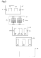
Fig. 3 is a plan view of a plurality of ceramic sheets, which are elements of the heat dissipation device ofFig. 2 . -
Fig. 4 is a cross-sectional view of the semiconductor device ofFig. 1 . -
Fig. 5A is a cross-sectional view ofFig. 4 taken along line 1-1, andFig. 5B is a cross-sectional view ofFig. 4 taken along line 2-2. -
Fig. 6 is a partially enlarged cross-sectional view of the semiconductor device ofFig. 4 . -
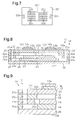
Fig. 7 is a plan view of another embodiment of a ceramic sheet. -
Fig. 8 is a cross-sectional view of a semiconductor device that includes the ceramic sheet ofFig. 7 . -
Fig. 9 is a partially enlarged cross-sectional view of another embodiment of a semiconductor device. -
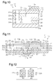
Fig. 10 is a partially enlarged cross-sectional view of another embodiment of a semiconductor device. -
Fig. 11 is a cross-sectional view of another embodiment of a semiconductor device. -
Fig. 12 is a plan view of another embodiment of a ceramic sheet. -
Fig. 13 is a cross-sectional view of another embodiment of a semiconductor device. -
Fig. 14 is a partially enlarged cross-sectional view of the semiconductor device ofFig. 13 . -
Fig. 15 is a plan view of a plurality of ceramic sheets, which are elements of a heat dissipation device of the semiconductor device ofFig. 13 . -
Fig. 16 is a perspective view of a second embodiment of a heat dissipation device. -
Fig. 17 is a perspective view of a semiconductor device that includes the heat dissipation device ofFig. 16 . -
Fig. 18 is a cross-sectional view ofFig. 17 taken along line 3-3. -
Fig. 19 is a cross-sectional view ofFig. 17 taken along line 4-4. -
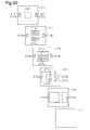
Fig. 20 is a plan view of a plurality of ceramic sheets, which are elements of a base body of the heat dissipation device ofFig. 16 . -
Fig. 21 is a cross-sectional view of another embodiment of a semiconductor device. - A first embodiment of the present invention will now be described with reference to
Figs. 1 to 6 . - A
semiconductor device 10 shown inFig. 1 is formed by mounting ametal plate 13b to which asemiconductor element 13a is coupled and ametal plate 14b to which asemiconductor element 14a is coupled on onesurface 12a (first surface) of abase body 12 of aheat dissipation device 11. Themetal plates semiconductor elements semiconductor elements metal plates metal plates heat dissipation device 11 by performing metallic joining, for example, soldering or brazing. In this manner, themetal plates first surface 12a of thebase body 12. - As shown in
Fig. 2 , in thefirst surface 12a of thebase body 12, locations where themetal plates Fig. 2 ) are respectively afirst mounting portion 121 and asecond mounting portion 131, which function as mounting portions on which themetal plates first surface 12a of thebase body 12. - The
base body 12 is formed by stacking a plurality of ceramic sheets (five sheets in the first embodiment). Thebase body 12 is baked to form theheat dissipation device 11. Aluminum oxide, silicon nitride, silicon carbide, aluminum nitride, alumina zirconium, or the like, is used as the material of the ceramic. Preferably, a ceramic material has high water resistance when water cooling is employed to cool theheat dissipation device 11. - As shown in
Fig. 3 , theheat dissipation device 11 of the first embodiment includes first to fifthceramic sheets heat dissipation device 11, the firstceramic sheet 21 is located at the upper side, and the fifthceramic sheet 25 is located at the lower side. The firstceramic sheet 21 forms a top plate portion of theheat dissipation device 11 and includes a surface (upper surface) defining thefirst surface 12a of thebase body 12. Acoolant supply hole 21 a and acoolant discharge hole 21 b extend through the firstceramic sheet 21. Thecoolant supply hole 21 a and thecoolant discharge hole 21 b have the same open area. Thecoolant supply hole 21 a is connected to a supply pipe P1 (shown inFigs. 1 and 2 ) that supplies a coolant to theheat dissipation device 11. Thecoolant discharge hole 21 b is connected to a discharge pipe P2 (shown inFigs. 1 and 2 ) that discharges the coolant out of theheat dissipation device 11 to the exterior. - A first
coolant inlet hole 22a extends through the secondceramic sheet 22. The firstcoolant inlet hole 22a is located at a position where the firstcoolant inlet hole 22a is overlapped with thecoolant supply hole 21 a as viewed from a stacking direction of the first to fifthceramic sheets coolant outlet hole 22b extends through the secondceramic sheet 22. The firstcoolant outlet hole 22b is located at a position where the firstcoolant outlet hole 22b is overlapped with thecoolant discharge hole 21 b as viewed from the stacking direction of the first to fifthceramic sheets coolant inlet hole 22a and the firstcoolant outlet hole 22b are located in symmetric positions. The firstcoolant inlet hole 22a and the firstcoolant outlet hole 22b have the same open area. - The second
ceramic sheet 22 also includes a plurality offirst slits 22c, which serve as slits, between the firstcoolant inlet hole 22a and the firstcoolant outlet hole 22b. Eachfirst slit 22c extends through the secondceramic sheet 22 and extends straight in the secondceramic sheet 22 from a position that is closer to the firstcoolant inlet hole 22a toward a central portion of the secondceramic sheet 22. Thefirst slits 22c have the same length. Thefirst slits 22c have the same open area. The first slits 22c are at least partially located underneath the first mounting portion 121 (metal plate 13b andsemiconductor element 13a). That is, thefirst slits 22c are at least partially overlapped with the first mountingportion 121 as viewed from the stacking direction A. - The second
ceramic sheet 22 also includes a plurality ofsecond slits 22d, which serve as slits, between the firstcoolant inlet hole 22a and the firstcoolant outlet hole 22b. Eachsecond slit 22d extends through the secondceramic sheet 22 and extends straight in the secondceramic sheet 22 from a position that is closer to the firstcoolant outlet hole 22b toward the central portion of the secondceramic sheet 22. The second slits 22d have the same length. The second slits 22d have the same open area. The second slits 22d are at least partially located underneath the second mounting portion 131 (metal plate 14b andsemiconductor element 14a). That is, thesecond slits 22d are at least partially overlapped with the second mountingportion 131 as viewed from the stacking direction A. - A second
coolant inlet hole 23a extends through the thirdceramic sheet 23. The secondcoolant inlet hole 23a is located in a position where the secondcoolant inlet hole 23a is overlapped with the firstcoolant inlet hole 22a as viewed from the stacking direction A. A secondcoolant outlet hole 23b extends through the thirdceramic sheet 23. The secondcoolant outlet hole 23b is located in a position where the secondcoolant outlet hole 23b is overlapped with the firstcoolant outlet hole 22b as viewed from the stacking direction A. The secondcoolant inlet hole 23a and the secondcoolant outlet hole 23b have the same open area. - The third
ceramic sheet 23 also includes afirst communication hole 23c, which extends in a direction orthogonal to the extending direction of eachfirst slit 22c. Thefirst communication hole 23c is partially overlapped with eachfirst slit 22c at one end that is located toward the firstcoolant inlet hole 22a as viewed from the stacking direction A. This communicates eachfirst slit 22c and thefirst communication hole 23c. Additionally, the thirdceramic sheet 23 includes asecond communication hole 23d at a position closer to the secondcoolant outlet hole 23b than thefirst communication hole 23c. Thesecond communication hole 23d extends in the direction orthogonal to the extending direction of eachfirst slit 22c. Thesecond communication hole 23d is partially overlapped with eachfirst slit 22c at the other end, which is located toward the firstcoolant outlet hole 22b, as viewed from the stacking direction A. This communicates eachfirst slit 22c and thesecond communication hole 23d. - The third
ceramic sheet 23 also includes athird communication hole 23e, which extends in a direction orthogonal to the extending direction of eachsecond slit 22d. Thethird communication hole 23e is partially overlapped with eachsecond slit 22d at one end that is located toward the firstcoolant inlet hole 22a as viewed from the stacking direction A. This communicates eachsecond slit 22d and thethird communication hole 23e. Additionally, the thirdceramic sheet 23 includes afourth communication hole 23f at a position closer to the secondcoolant outlet hole 23b than thethird communication hole 23e. Thefourth communication hole 23f extends in the direction orthogonal to the extending direction of eachsecond slit 22d. Thefourth communication hole 23f is partially overlapped with eachsecond slit 22d at the other end, which is located toward the firstcoolant outlet hole 22b, as viewed from the stacking direction A. This communicates eachsecond slit 22d and thefourth communication hole 23f. - The fourth
ceramic sheet 24 includes a first throughhole 24a, a second throughhole 24b, and a third throughhole 24c. The first throughhole 24a is overlapped with the secondcoolant inlet hole 23a and a portion of thefirst communication hole 23c as viewed from the stacking direction A. This communicates the secondcoolant inlet hole 23a and thefirst communication hole 23c. The second throughhole 24b is overlapped with a portion of thesecond communication hole 23d and a portion of thethird communication hole 23e as viewed from the stacking direction A. This communicates thesecond communication hole 23d and thethird communication hole 23e. Thethird communication hole 24c is overlapped with a portion of thefourth communication hole 23f and the secondcoolant outlet hole 23b as viewed from the stacking direction A. This communicates thefourth communication hole 23f and the secondcoolant outlet hole 23b. The fifthceramic sheet 25 forms a bottom plate portion of theheat dissipation device 11 and includes a surface (lower surface) defining asecond surface 12b of thebase body 12. That is, thefirst surface 12a and thesecond surface 12b are located at opposite sides of thebase body 12. - As shown in
Fig. 4 , thebase body 12 of theheat dissipation device 11 is formed by sequentially stacking the fourthceramic sheet 24, the thirdceramic sheet 23, the secondceramic sheet 22, and the firstceramic sheet 21 on the fifthceramic sheet 25. The interior of thebase body 12 includes thecoolant supply hole 21 a, the firstcoolant inlet hole 22a, the secondcoolant inlet hole 23a, the first throughhole 24a, thefirst communication hole 23c, eachfirst slit 22c, thesecond communication hole 23d, the second throughhole 24b, thethird communication hole 23e, eachsecond slit 22d, thefourth communication hole 23f, the third throughhole 24c, the secondcoolant outlet hole 23b, the firstcoolant outlet hole 22b, and thecoolant discharge hole 21 b, which form acoolant passage 15 through which a coolant flows. Thecoolant supply hole 21 a and thecoolant discharge hole 21 b open in thefirst surface 12a of thebase body 12. - The
second communication hole 23d, the second throughhole 24b, and thethird communication hole 23e form a portion of thecoolant passage 15 that is located between the first mountingportion 121 and the second mountingportion 131. That is, thesecond communication hole 23d, the second throughhole 24b, and thethird communication hole 23e form a portion of thecoolant passage 15 that extends from the first mountingportion 121 toward thesecond surface 12b and extends from thesecond surface 12b toward the second mountingportion 131. - In the first embodiment, the second
ceramic sheet 22 corresponds to a slit formation layer that includes thefirst slits 22c and thesecond slits 22d, which form a portion of thecoolant passage 15. Thefirst communication hole 23c corresponds to a communication passage that is overlapped with eachfirst slit 22c at a portion closer to the firstcoolant inlet hole 22a and communicates with eachfirst slit 22c. Thesecond communication hole 23d corresponds to a communication passage that is overlapped with eachfirst slit 22c at a portion closer to the secondcoolant outlet hole 23b and communications with thefirst slits 22c. Thethird communication hole 23e corresponds to a communication passage that is overlapped with eachsecond slit 22d at a portion closer to the firstcoolant inlet hole 22a and communicates with eachsecond slit 22d. Thefourth communication hole 23f corresponds to a communication passage that is overlapped with eachsecond slit 22d at a portion closer to the firstcoolant outlet hole 22b and communicates with eachsecond slit 22d. The thirdceramic sheet 23 corresponds to a communication passage formation layer that includes thefirst communication hole 23c, thesecond communication hole 23d, thethird communication hole 23e, and thefourth communication hole 23f, which correspond to the communication passages. - The first slits 22c and the
second slits 22d are located toward the first mountingportion 121 and the second mountingportion 131 from thefirst communication hole 23c, thesecond communication hole 23d, thethird communication hole 23e, and thefourth communication hole 23f in the stacking direction A. - In the
heat dissipation device 11, thesecond communication hole 23d is continuous to thefirst slit 22c at a downstream side of the coolant flow, and the second throughhole 24b is continuous to thesecond communication hole 23d. This forms an extension passage W that extends from thefirst surface 12a to thesecond surface 12b of thebase body 12. As shown inFigs. 4 and 6 , the extension passage W includes a passage surface X1 and a passage surface Y1 that are opposed in the stacking direction of the first to fifthceramic sheets 21 to 25. The passage surface X1 is a portion of a passage formed by thefirst slit 22c, which is located closer to thefirst surface 12a of thebase body 12. The passage surface Y1 is a portion of a passage formed by the second throughhole 24b, which is located closer to thesecond surface 12b. - The passage surface X1 is formed by a surface of the first
ceramic sheet 21, which is located above the secondceramic sheet 22. The passage surface Y1 is formed by a surface of the fifthceramic sheet 25, which is located below the fourthceramic sheet 24. That is, a passage formed by thefirst slit 22c forms thecoolant passage 15 that is located on the uppermost position in the stacking direction. The passage surface X1 corresponds to an upper surface of the passage. A passage formed by the second throughhole 24b forms thecoolant passage 15 that is located at the lowermost position in the stacking direction. The passage surface Y1 corresponds to a lower surface of the passage. - As shown in
Fig. 5A , afirst fin 31 is located between adjacent ones of thefirst slits 22c. As shown inFig. 5B , asecond fin 32 is located between adjacent ones of thesecond slits 22d. - As shown in
Fig. 6 , the length H of the first fin 31 (length of thefirst slit 22c) is set to be within a region Z (dotted region inFig. 6 ) as viewed from the stacking direction A. In a cross-section of the firstceramic sheet 21, the region Z is located between straight lines A and B. The straight lines A and B extend fromopposite ends 131 band 132b of themetal plate 13b at an angle θ of 45° relative to thefirst surface 12a of thebase body 12. The angle θ of the straight lines A and B relative to thefirst surface 12a of thebase body 12 only needs to be within 30° to 60°. The region Z, which is located between the straight lines A and B, forms a heat transmission region where the heat generated by thesemiconductor element 13a is transmitted to theheat dissipation device 11 through themetal plate 13b. - In the first embodiment, a portion of the
first communication hole 23c that corresponds to the region Z as viewed from the stacking direction A serves as an overlappingportion 35 of eachfirst slit 22c and thefirst communication hole 23c. Thus, the overlappingportion 35 is located in the heat transmission region, where the heat generated by thesemiconductor element 13a is transmitted to theheat dissipation device 11 through themetal plate 13b. That is, the overlappingportion 35 is located proximate to a region where the first mountingportion 121 is located as viewed from the stacking direction A. The overlappingportion 35 is located toward an inner side of thefirst slit 22c from oneend 221c of eachfirst slit 22c that is closer to the firstcoolant inlet hole 22a. The same description can be given for the length of the second fin 32 (length of thesecond slit 22d) and an overlapping portion 36 of eachsecond slit 22d and thethird communication hole 23e as the length H of thefirst fin 31 and the overlappingportion 35 of eachfirst slit 22c and thefirst communication hole 23c. Thus, a detailed description will not be given. - As shown in
Fig. 6 , in a cross-sectional view of theheat dissipation device 11, the overlappingportion 35 includes a first overlapping portion 35a, which is located underneath the first mountingportion 121, and a second overlapping portion 35b, which excludes the first overlapping portion 35a. The length of the second overlapping portion 35b is greater than the length of the first overlapping portion 35a. In this case, the phrase "the length of the second overlapping portion 35b is greater than the length of the first overlapping portion 35a" means, in the cross-sectional view of theheat dissipation device 11, the second overlapping portion 35b extends toward the firstcoolant inlet hole 22a, which results in the length of the second overlapping portion 35b being greater than the length of the first overlapping portion 35a. Although the first mountingportion 121 has been described here, the second mountingportion 131 has the same form. Here, the phrase of "underneath a mounting portion" refers to a region that is located toward thecoolant passage 15 from the mounting portion and corresponds to a region that is overlapped with the mounting portion as viewed from the stacking direction A. - The operation of the first embodiment will now be described.
- The coolant supplied from the coolant supply source flows from the supply pipe P1 to each
first slit 22c through thecoolant supply hole 21 a, the firstcoolant inlet hole 22a, the secondcoolant inlet hole 23a, the first throughhole 24a, and thefirst communication hole 23c. In this case, when the coolant flows from thefirst communication hole 23c to eachfirst slit 22c, the coolant is expelled from thefirst communication hole 23c into eachfirst slit 22c and directed toward the first mounting portion 121 (semiconductor element 13a andmetal plate 13b). This generates a jet flow in the coolant flowing from thefirst communication hole 23c to eachfirst slit 22c and agitates the coolant flowing through eachfirst slit 22c. As a result, the heat, which is transmitted from thesemiconductor element 13a to the heat dissipation device 11 (each first fin 31) through themetal plate 13b, is dissipated to the coolant flowing through eachfirst slit 22c more effectively than when, for example, the coolant flows through eachfirst slit 22c along the first mounting portion 121 (first surface 12a of the base body 12) after flowing along thefirst surface 12a. This improves the performance for cooling thesemiconductor element 13a. In the first embodiment, thesemiconductor element 13a corresponds to a first cooling subject. - Also, the coolant flows from each
first slit 22c to eachsecond slit 22d through thesecond communication hole 23d, the second throughhole 24b, and thethird communication hole 23e. In this case, when the coolant flows from thethird communication hole 23e to eachsecond slit 22d, the coolant is expelled from thethird communication hole 23e into eachsecond slit 22d to be directed toward the second mounting portion 131 (semiconductor element 14a andmetal plate 14b). This generates a jet flow in the coolant flowing from thethird communication hole 23e to eachsecond slit 22d and agitates the coolant flowing through eachsecond slit 22d. As a result, the heat, which is transmitted fromsemiconductor element 14a to the heat dissipation device 11 (each second fin 32) through themetal plate 14b, is dissipated to the coolant flowing through eachsecond slit 22d more effectively then when, for example, the coolant flows through eachsecond slit 22d along the second mounting portion 131 (first surface 12a of the base body 12) after flowing along thefirst surface 12a. This improves the performance for cooling thesemiconductor element 14a. In the first embodiment, thesemiconductor element 14a corresponds to a second cooling subject. - The coolant flows through each
second slit 22d and is discharged from the discharge pipe P2 and out of theheat dissipation device 11 through thefourth communication hole 23f, the third throughhole 24c, the secondcoolant outlet hole 23b, the firstcoolant outlet hole 22b, and thecoolant discharge hole 21 b. - Accordingly, the first embodiment has the advantages described below.
- (1) The
first slit 22c and thesecond slit 22d are located toward the first mountingportion 121 and the second mountingportion 131 from thefirst communication hole 23c, thesecond communication hole 23d, thethird communication hole 23e, and thefourth communication hole 23f in the stacking direction A. The overlappingportion 35 of eachfirst slit 22c and thefirst communication hole 23c and the overlapping portion 36 of eachsecond slit 22d and thethird communication hole 23e are respectively located proximate to regions where the first mountingportion 121 and the second mountingportion 131 are arranged. Thus, the coolant flowing from thefirst communication hole 23c to eachfirst slit 22c may be directed toward the first mountingportion 121. The coolant flowing from thethird communication hole 23e to eachsecond slit 22d may be directed toward the second mountingportion 131. This cools thesemiconductor elements first slit 22c and eachsecond slit 22d along the first mountingportion 121 and the second mountingportion 131. Thus, the performance for cooling thesemiconductor elements - (2) In the region Z corresponding to the first mounting
portion 121 on which a cooling subject is mounted, that is, the region Z serving as the heat transmission region described above, the length of the second overlapping portion 35b is greater than the length of the first overlapping portion 35a. When the coolant enters a coolant passage of a thin slit, turbulent flow is generated. However, there is a time-lag until the turbulent flow contributes to a thermal exchange. The length of the second overlapping portion 35b is greater than the length of the first overlapping portion 35a. This allows the coolant to cool the heat transmission region from a portion located at the upstream side and effectively cools thesemiconductor element 13a. Thus, the performance for cooling thesemiconductor element 13a may be improved. In the same manner as the first mountingportion 121, when the second mountingportion 131 and a third mountingportion 171 which will be described later, have the same form, the same advantage may be obtained even when a plurality of semiconductor elements are mounted on each mounting portion. - (3) A portion of the
coolant passage 15 that is formed by thesecond communication hole 23d, the second throughhole 24b, and thethird communication hole 23e extends from the first mountingportion 121 in a direction toward thesecond surface 12b and extends from thesecond surface 12b in a direction toward the second mountingportion 131. Thus, the flow of the coolant flowing through thecoolant passage 15 may be directed toward the first mountingportion 121 and the second mountingportion 131. Therefore, when themetal plate 13b, to which thesemiconductor element 13a is coupled, is mounted on the first mountingportion 121 and themetal plate 14b, to which thesemiconductor element 14a is coupled, is mounted on the second mountingportion 131, thesemiconductor elements semiconductor elements - (4) The
first communication hole 23c and thefirst slit 22c, and thesecond communication hole 23e and thesecond slit 22d, are each directed to the corresponding mounting portion in a stepped manner. The steppedcoolant passage 15 can generate a jet flow and a turbulent flow in the coolant. This effectively cools eachfirst slit 22c from theend 221c, which is located at the upstream side, and eachsecond slit 22d from an end of the passage surface X1 that is located at the upstream side. Thus, the cooling performance may be improved. This reduces the size of theheat dissipation device 11 without the need to lengthen the passage to improve the cooling performance. - (5) The
coolant supply hole 21 a and thecoolant discharge hole 21 b open in thefirst surface 12a of thebase body 12. This allows thefirst surface 12a of thebase body 12 to be connected to the supply pipe P1, which is used to supply the coolant, and the discharge pipe P2, which is used to discharge the coolant. Thus, components needed for theheat dissipation device 11 may be collectively located at the side of thefirst surface 12a of thebase body 12. This reduces the size of theheat dissipation device 11. - (6) The length H of the first fin 31 (length of the
first slit 22c) is set to be within the region Z as viewed from the stacking direction A. The region Z is located between the straight lines A and B, which extend from the opposite ends 131 b and 132b of themetal plate 13b at an angle θ of 45° relative to thefirst surface 12a of thebase body 12. In this case, the length H of thefirst fin 31 may be the minimum length needed for the heat dissipation of thesemiconductor element 13a. That is, the length of thefirst slit 22c can be minimized. This limits pressure loss of the coolant flowing through thefirst slit 22c as compared to when thefirst slit 22c is formed to extend beyond the region Z to a position outside the region Z. - (7) In the extension passage W, the passage surfaces X1 and Y1 are opposed to each other in the stacking direction. This reduces portions that decrease the area of the passage. Thus, the pressure loss of the coolant may be decreased. When the passage surfaces X1 and Y1 are opposed to each other, the extension passage W becomes almost straight in the stacking direction A. Thus, the reduction of steps in the extension passage W limits expansion of the
coolant passage 15 in the lateral direction. This decreases the size of theheat dissipation device 11. - The first embodiment may be modified as follows.
- As shown in
Fig. 7 , the secondceramic sheet 22 may include acommunication portion 22h that communicates eachfirst slit 22c and eachsecond slit 22d. As shown inFig. 8 , thesecond communication hole 23d, the second throughhole 24b, and thethird communication hole 23e may be removed. In this case, the coolant may flow from eachfirst slit 22c to eachsecond slit 22d through thecommunication portion 22h only in the secondceramic sheet 22. This smoothly flows the coolant compared to when the coolant flows from eachfirst slit 22c to eachsecond slit 22d through thesecond communication hole 23d, the second throughhole 24b, and thethird communication hole 23e. Thus, the pressure loss of the coolant may be limited. In this case, preferably, a metal plate including a semiconductor element that should be cooled the most is mounted on the first mountingportion 121. - As shown in
Fig. 9 , for example, the open area of thefirst communication hole 23c may be set to be smaller than that of the first embodiment. This increases the flow speed of the coolant when passing through thefirst communication hole 23c. In this case, jet flow may be generated in the coolant flowing from thefirst communication 23c to eachfirst slit 22c. As a result, the performance for cooling thesemiconductor element 13a may be further improved. In the same manner, the open area of thethird communication hole 23e may be set to be smaller than that of the first embodiment. This increases the flow speed of the coolant when passing through thethird communication hole 23e. - As shown in
Fig. 10 , for example, the open area of the first throughhole 24a may be set to be larger than that of the first embodiment. Also, in the same manner, the open area of the second throughhole 24b may be set to be larger than that of the first embodiment. - As shown in
Fig. 11 , a third mountingportion 171, which serves as a mounting portion, may be additionally located on a position of thesecond surface 12b that is located beyond a portion of thecoolant passage 15 that is located between the first mountingportion 121 and the second mountingportion 131 and extends in a direction from the first mountingportion 121 toward thesecond surface 12b of thebase body 12. In this case, the second throughhole 24b is replaced with a plurality ofslits 41, and a plurality offins 42 are arranged in the fourthceramic sheet 24. Thefins 42 are at least partially overlapped with the third mountingportion 171 as viewed from the stacking direction A. Ametal plate 17b to which asemiconductor element 17a is coupled is mounted on the third mountingportion 171. Thesemiconductor element 17a is cooled by dissipating heat to the coolant flowing through theslits 41. Thesemiconductor element 17a corresponds to a third cooling subject. In this case, the maximum number of semiconductor elements may be mounted on theheat dissipation device 11, the total volume may be reduced, and the performance for cooling thesemiconductor elements heat dissipation device 11, may be improved. - As shown in
Fig. 12 , the second ceramic sheet may include a plurality offirst slits 43 andsecond slits 44, each of which are undulated. This increases the heat dissipation surface area as compared to thefirst slits 22c and thesecond slits 22d, which are straight in a plan view. Also, the agitation effect is obtained. This further improves the performance for cooling thesemiconductor elements - In the first embodiment, the positions of the coolant supply hole and the coolant discharge hole of the
coolant passage 15 may be changed. For example, the coolant supply hole and the coolant discharge hole may open in thesecond surface 12b of thebase body 12. - In the first embodiment, the
first slits 22c and thesecond slits 22d only need to be at least partially overlapped with a region that includes the first mountingportion 121 and the second mountingportion 131 as viewed from the stacking direction A. - In the first embodiment, the number of the
first slits 22c and thesecond slits 22d may be changed. The number of slits is changed in accordance with the area of a semiconductor element, the passage width of thecoolant passage 15, and the like. For example, when the region area forming thecoolant passage 15 is the same, the number of slits decreases if the passage width increases, and the number of slits increases if the passage width decreases. - In the first embodiment, the number of ceramic sheets that are stacked to form the
base body 12 of theheat dissipation device 11 may be changed. For example, the number of ceramic sheets stacked is increased or decreased in accordance with the cross-sectional area (passage area) of thecoolant passage 15 formed in theheat dissipation device 11. - The first embodiment does not particularly limit the number of semiconductor elements or metal plates.
- The first embodiment does not particularly limit the number of mounting portions.
- In the first embodiment, the
heat dissipation device 11 may be cooled by undergoing air cooling. In this structure, a cooling gas, such as air, flows to thecoolant passage 15. - The
heat dissipation device 11 of the first embodiment shown inFig. 4 may include an extension passage, which has the same structure as the extension passage W, at the side of thesecond slit 22d in addition to the extension passage W connected to thefirst slit 22c. - As shown in
Figs. 13 and 14 , extension passages W1 and W2 extending straight in the stacking direction of the first to fifthceramic sheets 21 to 25 may be arranged as the extension passage W. The extension passage W1 is a portion of thecoolant passage 15 that is formed by thefirst slit 22c, thesecond communication hole 23d, and the second throughhole 24b. The extension passage W2 is a portion of thecoolant passage 15 that is formed by thesecond slit 22d, thefourth communication hole 23f, and the third throughhole 24c. As shown inFig. 14 , in the extension passage W1, the passage surface X1, which is formed by a surface of the firstceramic sheet 21, is opposed in the stacking direction to the passage surface Y1, which is formed by a surface of the fifthceramic sheet 25. The same applies to the extension passage W2. The straight extension passages W1 and W2 further decrease the pressure loss of the coolant compared to when the passage is formed in a stepped manner. Also, the reduction of steps further limits expansion of thecoolant passage 15 in the lateral direction. This further decreases the size of theheat dissipation device 11. - As shown in
Fig. 15 , when forming the straight extension passage W1, the position of thesecond communication hole 23d at an end (end that is located closer to the secondcoolant outlet hole 23b) opposite to the end that is located closer to the secondcoolant inlet hole 23a is aligned with the position of thefirst slit 22c at an end (end that is located closer to the firstcoolant outlet hole 22b) opposite to the end that is located closer to the firstcoolant inlet hole 22a. Also, when forming the extension passage W1, the position of thesecond communication hole 23d at the end that is located closer to the secondcoolant inlet hole 23a is aligned with the position of the second throughhole 24b at an end that is located closer to the first throughhole 24a. When forming the straight extension passage W2, the position of thefourth communication hole 23f at an end that is located closer to the secondcoolant outlet hole 23b is aligned with the position of thesecond slit 22d at an end that is located closer to the firstcoolant outlet hole 22b. Also, when forming the extension passage W2, the position of thefourth communication hole 23f at an end (end that is located closer to the secondcoolant inlet hole 23a) opposite to the end that is located closer to the secondcoolant outlet hole 23b is aligned with the position of the third throughhole 24c at an end that is located closer to the second throughhole 24b. - A second embodiment of the present invention will now be described with reference to
Figs. 16 to 20 . - As shown in
Fig. 16 , aheat dissipation device 11 includes abase body 218, which is formed by stacking a plurality of sheets (six sheets in the second embodiment) of first to sixthceramic members heat dissipation device 11. - The
base body 218 includes acoolant supply hole 219 and acoolant discharge hole 220. A coolant is supplied from the exterior to a coolant passage formed in thebase body 218 through thecoolant supply hole 219. The coolant flowing through the coolant passage is discharged from the coolant passage to the outside of thebase body 218 through thecoolant discharge hole 220. Thecoolant supply hole 219 and thecoolant discharge hole 220 each open in the firstceramic member 212, which is an element of thebase body 218. That is, thecoolant supply hole 219 and thecoolant discharge hole 220 each open in one surface (first surface) of thebase body 218. Thecoolant supply hole 219 is connectable to the supply pipe P1, which is connected to an external coolant supply source. Thecoolant discharge hole 220 is connectable to the discharge pipe P2, which discharges the coolant to the exterior. Thebase body 218 also includes a mounting portion 222 (indicated by broken lines inFig. 16 ) of anelectronic component 221 at a position where the mountingportion 222 is at least partially overlapped with the coolant passage as viewed from a stacking direction of the first to sixthceramic members portion 222 is arranged on a surface (first face) of the firstceramic member 212 located at the exterior of thebase body 218 in which thecoolant supply hole 219 and thecoolant discharge hole 220 open. - As shown in
Fig. 17 , in the same manner as the first embodiment, asemiconductor device 10 is formed by mounting ametal plate 227 on the mountingportion 222 located on thebase body 218 of theheat dissipation device 11. Asemiconductor element 226, which serves as theelectronic component 221, is coupled to themetal plate 227. Themetal plate 227, which functions as a wiring layer and a bonding layer, is pure aluminum (e.g., 1000 series aluminum, which is pure aluminum for industrial use) or copper. Thesemiconductor element 226 is, for example, an insulated gate bipolar transistor (IGBT) or a diode. Thesemiconductor element 226 and themetal plate 227, and themetal plate 227 and theheat dissipation device 11, are each joined by performing metallic joining, for example, soldering or brazing. - The
heat dissipation device 11 of the second embodiment will now be described in detail. - As shown in
Figs. 18 and 19 , acoolant passage 228 that communicates thecoolant supply hole 219 and thecoolant discharge hole 220 is formed in thebase body 218 of theheat dissipation device 11. In the description hereafter, the firstceramic member 212, which is the element of thebase body 218 and includes the mountingportion 222, is located at the upper side, and the sixthceramic sheet 217, which is located at the farthest position from the firstceramic member 212, is located at the lower side. - The
coolant passage 228 includes first to seventh passages L1 to L7. More specifically, the first passage L1 is straight and continuous to the coolant supply hole 291. The coolant flows through the first passage L1 in a vertically lower direction. The second passage L2 branches from the first passage L1. The coolant flows through the second passage L2 obliquely upward. The third passage L3 is straight, continuous to the second passage L2, and formed underneath the mountingportion 222. The coolant flows through the third passage L3 in the horizontal direction. The fourth passage L4 is straight and continuous to the third passage L3. The coolant flows through the fourth passage L4 in the vertically lower direction. The fifth passage L5 is straight and continuous to the fourth passage L4. The coolant flows through the fifth passage L5 in the horizontal direction. The sixth passage L6 is straight and continuous to the fifth passage L5. The coolant flows through the sixth passage L6 in a vertically direction. The seventh passage L7 is straight and branches from the first passage L1 together with the second passage L2. The coolant flows through the seventh passage L7 from the vertically lower side to the vertically upper side toward the third passage L3 located underneath the mountingportion 222. The first to sixthceramic members 212 to 217 includes a plurality of passage holes, which are elements of thecoolant passage 228. The passage holes are joined in the stacking direction of the first to sixthceramic members 212 to 217 to form the first to seventh passages L1 to L7. - Each member of the
heat dissipation device 11 will now be described with reference toFig. 20 . InFig. 20 , a sheet forming the ceramic member is referred to as a ceramic sheet. The same reference numeral as the ceramic member is given to the ceramic sheet. - As shown in
Fig. 20 , in the second embodiment, the first to sixthceramic sheets 212 to 217, which are elements of theheat dissipation device 11, are rectangle and have the same length and the same width. - The first
ceramic sheet 212 forms a top plate of theheat dissipation device 11 where the mountingportion 222 is located. Afirst passage hole 212a including thecoolant supply hole 219 and asixth passage hole 212b including thecoolant discharge hole 220 are located at opposite ends of the mountingportion 222. Thefirst passage hole 212a and thesixth passage hole 212b have the same open area. - The second
ceramic sheet 213 is located below the firstceramic sheet 212 when stacked. The secondceramic sheet 213 includes afirst passage hole 213a and asixth passage hole 213b. Thefirst passage hole 213a is located at a position corresponding to thefirst passage hole 212a of the firstceramic sheet 212 and communicates with thefirst passage hole 212a. Thefirst passage hole 213a has the same open area as thefirst passage hole 212a. Thesixth passage hole 213b is located at a position corresponding to thesixth passage hole 212b of the firstceramic sheet 212 and communicates with thesixth passage hole 212b. Thesixth passage hole 213b has the same open area as thesixth passage hole 212b. Also, the secondceramic sheet 213 includes a plurality of slit-like third passage holes 213c (five slits in the second embodiment) between thefirst passage hole 213a and thesixth passage hole 213b. Eachthird passage hole 213c has the same shape and extends straight. The length of thethird passage hole 213c in the extending direction (longitudinal direction) is greater than the length of the mountingportion 222 in the same direction. The third passage holes 213c are arranged along a direction orthogonal to the extending direction (longitudinal direction) at regular intervals. As shown inFigs. 18 and 19 , a portion of thethird passage hole 213c is located underneath the mountingportion 222. The other portion of thethird passage hole 213c is located outside the mountingportion 222 as viewed from the stacking direction B. - The third
ceramic sheet 214 is located below the secondceramic sheet 213 when stacked. The thirdceramic sheet 214 includes afirst passage hole 214a and asixth passage hole 214b. Thefirst passage hole 214a is located at a position corresponding to thefirst passage hole 213a of the secondceramic sheet 213 and communicates with thefirst passage hole 213a. Thefirst passage hole 214a has the same open area as thefirst passage hole 213a. Thesixth passage hole 214b communicates with thesixth passage hole 213b of the secondceramic sheet 213 and has the same open area as thesixth passage hole 213b. The thirdceramic sheet 214 also includes a plurality of slit-like third passage holes 214c (five slits in the second embodiment) between thefirst passage hole 214a and thesixth passage hole 214b. Eachthird passage hole 214c has the same shape and extends straight. Eachthird passage hole 214c is located in a position where thethird passage hole 214c is partially overlapped with thethird passage hole 213c of the secondceramic sheet 213 as viewed from the stacking direction B. The length of eachthird passage hole 214c in the extending direction (longitudinal direction) is greater than the length of thethird passage hole 213c of the secondceramic sheet 213 in the same direction. The third passage holes 214c are arranged along a direction orthogonal to the extending direction (longitudinal direction) at regular intervals. When the secondceramic sheet 213 and the thirdceramic sheet 214 are stacked, opposite ends of thethird passage hole 214c are located at positions that are projected by the same length outward from opposite ends of thethird passage hole 213c as viewed from the stacking direction B. - As shown in
Fig. 19 , when the secondceramic sheet 213 and the thirdceramic sheet 214 are stacked, eachthird passage hole 213c are overlapped with eachthird passage hole 214c in the stacking direction. This forms the third passage L3, which has the height of two ceramic sheets. - The fourth
ceramic sheet 215 is located below the thirdceramic sheet 214 when stacked. The fourthceramic sheet 215 includes afirst passage hole 215a. When the thirdceramic sheet 214 is stacked, thefirst passage hole 215a is located at a position where thefirst passage hole 215a is entirely overlapped with thefirst passage hole 214a and partially overlapped with thethird passage hole 214c that is located closer to thefirst passage hole 214a as viewed from the stacking direction B. The open area of thefirst passage hole 215a is greater than the open area of thefirst passage hole 214a of the thirdceramic sheet 214. The length of thefirst passage hole 215a in a direction orthogonal to the extending direction of thethird passage hole 214c of the thirdceramic sheet 214 is the same as the length between inner surfaces of the third passage holes 214c that are located at the opposite outermost positions. - The fourth
ceramic sheet 215 includes asixth passage hole 215b. Thesixth passage hole 215b is located at a position corresponding to thesixth passage hole 214b of the thirdceramic sheet 214 and communicates with thesixth passage hole 214b. Thesixth passage hole 215b has the same open area as thesixth passage hole 214b. The fourthceramic sheet 215 also includes afourth passage hole 215c between thefirst passage hole 215a and thesixth passage hole 215b. Thefourth passage hole 215c is located in a position where thefourth passage hole 215c is partially overlapped with eachthird passage hole 214c that is located closer to thesixth passage hole 214b as viewed from the stacking direction B. - The fourth
ceramic sheet 215 also includes a plurality of slit-like seventh passage holes 215d (five slits in the second embodiment) between thefirst passage hole 215a and thefourth passage hole 215c. Eachseventh passage hole 215d has the same shape and extends straight. Eachseventh passage hole 215d is located in a position where theseventh passage hole 215d is overlapped with thethird passage hole 214c of the thirdceramic sheet 214 as viewed from the stacking direction B. The length of eachseventh passage hole 215d in the extending direction (longitudinal direction) is less than the length of each of the third passage holes 213c and 214c of the second and thirdceramic sheets seventh passage holes 215d are arranged along a direction orthogonal to the extending direction (longitudinal direction) at regular intervals. The centers of theseventh passage holes 215d are arranged along a line that extends through the center of the mountingportion 222 in a direction orthogonal to the extending direction of the third passage holes 213c and 214c. - The fifth
ceramic sheet 216 is located below the fourthceramic sheet 215 when stacked. The fifthceramic sheet 216 includes afirst passage hole 216a and afifth passage hole 216b. When the fourthceramic sheet 215 is stacked, thefirst passage hole 216a is located at a position where thefirst passage hole 216a is entirely overlapped with thefirst passage hole 215a and eachseventh passage hole 215d as viewed from the stacking direction B. Also, when the fourthceramic sheet 215 is stacked, thefifth passage hole 216b is located at a position where thefifth passage hole 216b is entirely overlapped with thesixth passage hole 215b and thefourth passage hole 215c as viewed from the stacking direction B. The sixthceramic sheet 217 is located below the fifthceramic sheet 216 when stacked. The sixthceramic sheet 217 forms a bottom plate of theheat dissipation device 11. - The
base body 218 of theheat dissipation device 11 is formed by sequentially stacking the fifthceramic member 216, the fourthceramic member 215, the thirdceramic member 214, the secondceramic member 213, and the firstceramic member 212 on the sixthceramic member 217. As described above, thecoolant passage 228 is formed in thebase body 218 having such a structure. - The first passage L1 is formed by connecting each
first passage hole ceramic members 212 to 216. The second passage L2 is formed by connecting a portion of thefirst passage hole 215a of the fourthceramic member 215, a portion of thethird passage hole 214c of the thirdceramic member 214, and a portion of thethird passage hole 213c of the secondceramic member 213 in a stepped manner. The third passage L3 is formed by connecting thethird passage hole 213c of the secondceramic member 213 and thethird passage hole 214c of the thirdceramic member 214. - The fourth passage L4 is formed by connecting a portion of the
third passage hole 214c of the thirdceramic member 214, thefourth passage hole 215c of the fourthceramic member 215, and a portion of thefifth passage hole 216b of the fifthceramic member 216 in a straight line. The fifth passage L5 is formed by thefifth passage hole 216b of the fifthceramic member 216, which is connected to thefourth passage hole 215c of the fourthceramic member 215. The sixth passage L6 is connected to thefifth passage hole 216b of the fifthceramic member 216 and formed by connecting eachsixth passage hole ceramic members 212 to 215. The seventh passage L7 is formed by the seventh passage holes 215d of the fourthceramic member 215, which are connected to thefirst passage hole 216a of the fifthceramic member 216. - The third passage L3 of the second embodiment serves as an underneath-lying passage through which coolant flows underneath the mounting
portion 222. The second passage L2 of the second embodiment is in communication with the third passage L3 at the upstream side in a flow direction of the coolant and forms a supply passage that supplies the coolant to the third passage L3 together with the first passage L1 connected to the second passage L2. The fourth passage L4 of the second embodiment is in communication with the third passage L3 at the downstream side in the flow direction of the coolant and forms a discharge passage that discharges the coolant from the third passage L3 together with the fifth passage L5 connected to the fourth passage L4 and the sixth passage L6 connected to the fifth passage L5. The seventh passage L7 of the second embodiment is located between the supply passage and the discharge passage and serves as an expulsion passage that expels the coolant to the third passage L3 from the vertically lower side toward the vertically upper side. The seventh passage L7 serving as the expulsion passage expels the coolant toward a central section of the mountingportion 222. - As shown in
Fig. 19 , thebase body 218 includesfins fin 230 is located between the third passage holes 213c of the secondceramic member 213 forming the third passage L3. Thefin 231 is located between the third passage holes 214c of the thirdceramic member 214 forming the third passage L3. Thefins fins - The operation of the second embodiment will now be described.
- In the
heat dissipation device 11 of the second embodiment, the coolant supplied through thecoolant supply hole 219 to thecoolant passage 228 first flows through the first passage L1 toward a lower side of theheat dissipation device 11. The coolant in the first passage L1 is separated to flow into the second passage L2 and the seventh passage L7, which branch from the first passage L1. Then, the coolant flows from the second passage L2 and the seventh passage L7 to the third passage L3. The heat of the electronic component 221 (semiconductor element 226 and metal plate 227) is dissipated to the coolant flowing through the third passage L3 by way of the surface of the firstceramic member 212, which covers the third passage L3, and thefins coolant discharge hole 220. - The
heat dissipation device 11 of the second embodiment includes the second passage L2, through which the coolant flows toward the third passage L3 in an oblique direction from a peripheral region of the mountingportion 222 of theelectronic component 221 toward the mountingportion 222, and the seventh passage L7, through which the coolant flows toward the central section of the mountingportion 222 from the lower side to the upper side. The coolant flowing through the second passage L2 and the seventh passage L7 are expelled toward the third passage L3 from the lower side to the upper side. This generates a jet flow in the coolant flowing through the third passage L3 and agitates the coolant. The agitation thins a temperature boundary layer of the coolant flowing through the third passage L3. Particularly, the coolant is expelled from the seventh passage L7 toward the central portion of theelectronic component 221, which has the highest temperature in the mountingportion 222. This allows the coolant to directly strike a heating surface and effectively thins the temperature boundary layer. - Accordingly, the second embodiment has the advantages described below.
- (8) The seventh passage L7 is arranged to expel the coolant into the third passage L3 from the vertically lower side to the vertically upper side. This allows the coolant to directly strike a location corresponding to the mounting
portion 222. This effectively agitates the coolant flowing through the third passage L3 and thins the temperature boundary layer of the coolant flowing through the third passage L3. Thus, the performance for cooling the cooling subject can be improved. - (9) The seventh passage L7 branches from the first passage L1. This simplifies the structure of the
coolant passage 228 formed in thebase body 218. - (10) The seventh passage L7 expels the coolant toward the central section of the mounting
portion 222. This effectively thins the temperature boundary layer of the coolant flowing through the third passage L3. Thus, the performance for cooling the cooling subject can be further improved. - (11) The
coolant supply hole 219 and thecoolant discharge hole 220 open in the surface (first surface) of thebase body 218 where the mountingportion 222 is arranged. This allows for a collective arrangement of components needed for theheat dissipation device 11, such as, the supply pipe P1 connected to thecoolant supply hole 219, and the discharge pipe P2 connected to thecoolant discharge hole 220. As a result, theheat dissipation device 11 can be reduced in size. - (12) The coolant is expelled from the second passage L2 and the seventh passage L7 toward the third passage L3. This effectively agitates the coolant flowing through the third passage L3 and thins the temperature boundary layer of the coolant flowing through the third passage L3.
- (13) The straight fourth passage L4 decreases pressure loss of the coolant as compared to when the fourth passage L4 includes steps. Also, the straight fourth passage L4 reduces steps in the
coolant passage 228 and limits expansion of thecoolant passage 228 in the lateral direction. This reduces the size of theheat dissipation device 11. - (14) The
semiconductor device 10 having theheat dissipation device 11 can effectively cool the electronic component 221 (semiconductor element 226 and metal plate 227). This improves the performance for cooling theelectronic component 221. - (15) The ceramic
heat dissipation device 11 may have a cooling function and an insulative property. This allows for the formation of thesemiconductor device 10 by directly joining theheat dissipation device 11 with the electronic component 221 (semiconductor element 226 and metal plate 227). Thus, thesemiconductor device 10 may be reduced in size and the number of components. - The second embodiment may be modified as follows.
- As shown in
Fig. 21 , in the second embodiment, a plurality of the seventh passages L7 may be arranged in thecoolant passage 228. When a plurality of the seventh passages L7 are used, coolant expelling positions of the seventh passages L7 are located within the region of the mountingportion 222 as viewed from the stacking direction B. This further increases the effect of the jet flow. Preferably, at least one of the seventh passages L7 is located in a position where the coolant is expelled toward the central section of the mountingportion 222. In this structure, the seventh passages L7 allow the coolants to directly strike a location corresponding to the mountingportion 222 from a wide range. This effectively thins the temperature boundary layer of the coolant flowing through the third passage L3 and further improves the performance for cooling the cooling subject. - In the second embodiment, the
base body 218 may include undulated fins by forming undulated third passage holes 213c and 214c. The undulated fins increase the area that contacts the coolant and has a coolant agitating effect. This improves the cooling performance. - In the second embodiment, a passage that supplies the coolant to the second passage L2 may differ from a passage that supplies the coolant to the seventh passage L7. For example, the coolant may be directly supplied to the seventh passage L7 from the exterior.
- In the second embodiment, the
coolant supply hole 219 and thecoolant discharge hole 220 may be located at different positions in thebase body 218. For example, thecoolant supply hole 219 and thecoolant discharge hole 220 may be located in the sixthceramic member 217. One of thecoolant supply hole 219 and thecoolant discharge hole 220 may be located in the firstceramic member 212 when the other is located in the sixthceramic member 217. - In the second embodiment, the fourth passage L4 may extend obliquely downward by connecting a portion of the
third passage hole 214c of the thirdceramic member 214, thefourth passage hole 215c of the fourthceramic member 215, and a portion of thefifth passage hole 216b of the fifthceramic member 216 in a stepped manner. - In the second embodiment, the number of the third passage holes 213c and 214c may be changed. The number is changed in accordance with the area of a semiconductor element, the passage width of the
coolant passage 228, and the like. For example, when the area of the region forming thecoolant passage 228 is the same, the number of the third passage holes 213c and 214c decreases if the passage width increases, and the number increases if the passage width decreases. - In the second embodiment, the number of ceramic members that are stacked to form the
base body 218 of theheat dissipation device 11 may be changed. For example, the number of ceramic members stacked is increased or decreased in accordance with the cross-sectional area (passage area) of thecoolant passage 228 formed in theheat dissipation device 11. - In the second embodiment, the
heat dissipation device 11 may be cooled by undergoing liquid cooling or air cooling. - In the second embodiment, the number of the
electronic components 221 mounted on theheat dissipation device 11 may be changed. Thecoolant passage 228 in thebase body 218 may be modified in accordance with the number or the layout of the mountingportions 222 on which theelectronic components 221 are mounted. -
- 10
- semiconductor device
- 11
- heat dissipation device
- 12, 218
- base body
- 12a
- first surface
- 12b
- second surface
- 13a, 14a, 17a, 226
- semiconductor element (cooling subject)
- 13b, 14b, 17b, 227
- metal plate
- 15, 228
- coolant passage
- 21
- first ceramic sheet serving as ceramic sheet
- 21 a, 219
- coolant supply hole
- 21b, 220
- coolant discharge hole
- 22
- second ceramic sheet serving as ceramic sheet corresponding to slit formation layer
- 22c, 43
- first slit serving as slit
- 22d, 44
- second slit serving as slit
- 22h
- communication portion
- 23
- third ceramic sheet serving as ceramic sheet corresponding to communication passage formation layer
- 23c
- first communication hole corresponding to communication passage
- 23d
- second communication hole corresponding to communication passage
- 23e
- third communication hole corresponding to communication passage
- 23f
- fourth communication hole corresponding to communication passage
- 24
- fourth ceramic sheet serving as ceramic sheet
- 25
- fifth ceramic sheet serving as ceramic sheet
- 35, 36
- overlapping portion
- 41
- slit
- 121
- first mounting portion serving as mounting portion
- 131
- second mounting portion serving as mounting portion
- 171
- third mounting portion serving as mounting portion
- 212 to 217
- first to sixth ceramic members (ceramic sheets)
- 222
- mounting portion
- 212a, 213a, 214a, 215a, 216a
- first passage hole
- 212b, 213b, 214b, 215b
- sixth passage hole
- 213c, 214c
- third passage hole
- 215c
- fourth passage hole
- 215d
- seventh passage hole
- 216b
- fifth passage hole
- W, W1, W2
- extension passage
- X1, Y1
- passage surface
- L1 to L7
- first to seventh passages
Claims (13)
- A heat dissipation device comprising:a base body formed by stacking a plurality of ceramic sheets;a coolant passage located in the base body, wherein coolant flows through the coolant passage;at least one mounting portion defined in a first surface of the base body as a location where a cooling subject is mounted;a slit formation layer formed by at least one of the ceramic sheets, wherein the slit formation layer includes a plurality of slits that form a portion of the coolant passage, and the slits are formed to be at least partially overlapped with a region that includes the mounting portion as viewed from a stacking direction of the ceramic sheets; anda communication passage formation layer formed by at least one of the ceramic sheets, wherein the communication passage formation layer forms a portion of the coolant passage and includes a communication passage that communicates the slits, and the slits are located toward the mounting portion from the communication passage in the stacking direction of the ceramic sheets,wherein an overlapping portion of the slits and the communication passage is located proximate to a region where the mounting portion is located as viewed from the stacking direction.
- The heat dissipation device according to claim 1, wherein, in a cross-sectional view, the overlapping portion, which is located at a upstream side of the coolant passage in correspondence with the mounting portion, includes a first overlapping portion that is located underneath the mounting portion and a second overlapping portion that excludes the first overlapping portion, and the length of the second overlapping portion is greater than the length of the first overlapping portion.
- The heat dissipation device according to claim 1 or 2, wherein
a plurality of the mounting portions are arranged side by side on the first surface of the base body,
a portion of the coolant passage that is located between adjacent ones of the mounting portions as viewed from the stacking direction extends from one of the adjacent ones of the mounting portions toward a second surface of the base body that is located at the opposite side of the first surface and further extends from the second surface toward the other of the adjacent ones of the mounting portions. - The heat dissipation device according to claim 3, wherein
the base body further includes a mounting portion on which a different cooling subject is mounted, wherein the mounting portion is located in the second surface where a portion of the coolant passage from one of the adjacent ones of the mounting portions toward the second surface extends to. - The heat dissipation device according to any one of claims 1 to 4, wherein
an extension passage extends from a downstream side of the slits of the slit formation layer in a direction the coolant flows toward the second surface of the base body, which is located at the opposite side of the first surface, and
a portion of a passage surface of the extension passage that is located closer to the first surface is opposed to a portion of a passage surface of the extension passage that is located closer to the second surface in the stacking direction. - The heat dissipation device according to claim 3,
the slit formation layer includes a plurality of first slits, a plurality of second slits, and a communication portion that communicates a plurality of the first slits and a plurality of the second slits,
the first slits are at least partially overlapped with a region that includes one of the adjacent ones of the mounting portions as viewed from the stacking direction, and
the second slits are at least partially overlapped with a region that includes the other of the adjacent ones of the mounting portions as viewed from the stacking direction. - The heat dissipation device according to claim 1, wherein the coolant passage includes
an underneath-lying passage formed underneath the mounting portion,
a supply passage in communication with an upstream side of the underneath-lying passage in a direction the coolant flows, wherein the supply passage supplies the coolant to the underneath-lying passage,
a discharge passage in communication with a downstream side of the underneathlying passage in the direction the coolant flows, wherein the discharge passage discharges the coolant from the underneath-lying passage, and
an expulsion passage located between the supply passage and the discharge passage, wherein the expulsion passage expels the coolant to the underneath-lying passage from a vertically lower side toward a vertically upper side. - The heat dissipation device according to claim 7, wherein the expulsion passage branches from the supply passage.
- The heat dissipation device according to claim 7 or 8 comprising a plurality of the expulsion passages.
- The heat dissipation device according to any one of claims 7 to 9, wherein the expulsion passage expels the coolant toward a central section of the mounting portion.
- A heat dissipation device comprising:a base body formed by stacking a plurality of ceramic members;a coolant passage located in the base body; andat least one mounting portion defined in a first surface of the base body as a location where a cooling subject is mounted,wherein the coolant passage includes
an underneath-lying passage that is formed underneath the mounting portion,
a supply passage in communication with an upstream side of the underneath-lying passage in a direction coolant flows, wherein the supply passage supplies the coolant to the underneath-lying passage,
a discharge passage in communication with a downstream side of the underneathlying passage in the direction the coolant flows, wherein the discharge passage discharges the coolant from the underneath-lying passage, and
an expulsion passage located between the supply passage and the discharge passage, wherein the expulsion passage expels the coolant to the underneath-lying passage from a vertically lower side toward a vertically upper side. - The heat dissipation device according to any one of claims 1 to 11, wherein the coolant passage includes a coolant supply hole and a coolant discharge hole that open in the first surface of the base body.
- A semiconductor device comprising:the heat dissipation device according to any one of claims 1 to 12;a metal plate mounted on the mounting portion of the heat dissipation device; anda semiconductor element coupled to the metal plate.
Applications Claiming Priority (4)
| Application Number | Priority Date | Filing Date | Title |
|---|---|---|---|
| JP2012159734 | 2012-07-18 | ||
| JP2012284012 | 2012-12-27 | ||
| JP2012284011 | 2012-12-27 | ||
| PCT/JP2013/069515 WO2014014054A1 (en) | 2012-07-18 | 2013-07-18 | Heat dissipation device and semiconductor device |
Publications (2)
| Publication Number | Publication Date |
|---|---|
| EP2876678A1 true EP2876678A1 (en) | 2015-05-27 |
| EP2876678A4 EP2876678A4 (en) | 2016-04-13 |
Family
ID=49948877
Family Applications (1)
| Application Number | Title | Priority Date | Filing Date |
|---|---|---|---|
| EP13820186.8A Withdrawn EP2876678A4 (en) | 2012-07-18 | 2013-07-18 | HEAT DISSIPATING DEVICE AND SEMICONDUCTOR DEVICE |
Country Status (6)
| Country | Link |
|---|---|
| US (1) | US9646915B2 (en) |
| EP (1) | EP2876678A4 (en) |
| JP (1) | JP6124890B2 (en) |
| KR (1) | KR101624523B1 (en) |
| CN (1) | CN104471706A (en) |
| WO (1) | WO2014014054A1 (en) |
Cited By (3)
| Publication number | Priority date | Publication date | Assignee | Title |
|---|---|---|---|---|
| EP3038152A1 (en) * | 2014-12-26 | 2016-06-29 | Kabushiki Kaisha Toshiba | Wiring board and semiconductor package including wiring board |
| EP3531054A1 (en) * | 2018-02-27 | 2019-08-28 | Shinko Electric Industries Co., Ltd. | Flat loop heat pipe |
| EP3531056A1 (en) * | 2018-02-27 | 2019-08-28 | Shinko Electric Industries Co., Ltd. | Loop type heat pipe |
Families Citing this family (9)
| Publication number | Priority date | Publication date | Assignee | Title |
|---|---|---|---|---|
| WO2016017697A1 (en) * | 2014-07-29 | 2016-02-04 | 京セラ株式会社 | Heat exchanger |
| DE102015114291B4 (en) | 2014-08-27 | 2022-01-05 | Rogers Germany Gmbh | Cooling arrangement |
| JP6502653B2 (en) * | 2014-11-26 | 2019-04-17 | 京セラ株式会社 | Cooling plate and semiconductor module |
| US10837718B2 (en) * | 2015-09-18 | 2020-11-17 | T.Rad Co., Ltd. | Laminated core type heat sink |
| JP6951786B2 (en) * | 2017-08-29 | 2021-10-20 | 株式会社Welcon | heat sink |
| DE102017121015A1 (en) | 2017-09-12 | 2019-03-14 | Rogers Germany Gmbh | Adapter element for connecting a component such as a laser diode to a heat sink, a system of a laser diode, a heat sink and an adapter element and method for producing an adapter element |
| CN111418055B (en) * | 2017-11-28 | 2024-03-12 | 京瓷株式会社 | Substrates for mounting electronic components, electronic devices and electronic modules |
| DE102018112000B4 (en) * | 2018-05-18 | 2024-08-08 | Rogers Germany Gmbh | System for cooling a metal-ceramic substrate, a metal-ceramic substrate and method for producing the system |
| JP7323975B2 (en) * | 2019-08-26 | 2023-08-09 | 株式会社ティラド | Laminated plate heat exchanger |
Family Cites Families (9)
| Publication number | Priority date | Publication date | Assignee | Title |
|---|---|---|---|---|
| FR2578099B1 (en) * | 1985-02-26 | 1987-12-04 | Eurofarad | MONOLITHIC SUBSTRATE FOR ELECTRONIC POWER COMPONENT, AND METHOD FOR THE PRODUCTION THEREOF |
| DE4315580A1 (en) * | 1993-05-11 | 1994-11-17 | Fraunhofer Ges Forschung | Arrangement comprising laser diodes and a cooling system, and method for its production |
| JP4031903B2 (en) * | 1999-10-21 | 2008-01-09 | イェーノプティク アクチエンゲゼルシャフト | Equipment for cooling diode lasers |
| JP2002327993A (en) * | 2001-05-01 | 2002-11-15 | Fujitsu Ltd | Thin heat pipe, thin heat sink, heat control system, and method of manufacturing thin heat pipe |
| JP2004095599A (en) * | 2002-08-29 | 2004-03-25 | Denso Corp | Stack cooler |
| JP4721412B2 (en) | 2005-06-28 | 2011-07-13 | 本田技研工業株式会社 | Cooler and manufacturing method thereof |
| JP2007184479A (en) * | 2006-01-10 | 2007-07-19 | Toyota Central Res & Dev Lab Inc | A cooler and a semiconductor device in which a semiconductor element is mounted on the cooler |
| JP4789813B2 (en) * | 2007-01-11 | 2011-10-12 | トヨタ自動車株式会社 | Semiconductor device cooling structure |
| WO2011136362A1 (en) * | 2010-04-28 | 2011-11-03 | 株式会社 豊田自動織機 | Heat dissipation device and semiconductor device |
-
2013
- 2013-07-18 US US14/414,728 patent/US9646915B2/en not_active Expired - Fee Related
- 2013-07-18 EP EP13820186.8A patent/EP2876678A4/en not_active Withdrawn
- 2013-07-18 WO PCT/JP2013/069515 patent/WO2014014054A1/en not_active Ceased
- 2013-07-18 KR KR1020157001315A patent/KR101624523B1/en not_active Expired - Fee Related
- 2013-07-18 JP JP2014525861A patent/JP6124890B2/en active Active
- 2013-07-18 CN CN201380037367.4A patent/CN104471706A/en active Pending
Cited By (5)
| Publication number | Priority date | Publication date | Assignee | Title |
|---|---|---|---|---|
| EP3038152A1 (en) * | 2014-12-26 | 2016-06-29 | Kabushiki Kaisha Toshiba | Wiring board and semiconductor package including wiring board |
| EP3531054A1 (en) * | 2018-02-27 | 2019-08-28 | Shinko Electric Industries Co., Ltd. | Flat loop heat pipe |
| EP3531056A1 (en) * | 2018-02-27 | 2019-08-28 | Shinko Electric Industries Co., Ltd. | Loop type heat pipe |
| US10883770B2 (en) | 2018-02-27 | 2021-01-05 | Shinko Electric Industries Co., Ltd. | Loop type heat pipe |
| US11143461B2 (en) | 2018-02-27 | 2021-10-12 | Shinko Electric Industries Co., Ltd. | Flat loop heat pipe |
Also Published As
| Publication number | Publication date |
|---|---|
| US9646915B2 (en) | 2017-05-09 |
| US20150221579A1 (en) | 2015-08-06 |
| JP6124890B2 (en) | 2017-05-10 |
| KR101624523B1 (en) | 2016-05-26 |
| KR20150032868A (en) | 2015-03-30 |
| WO2014014054A1 (en) | 2014-01-23 |
| JPWO2014014054A1 (en) | 2016-07-07 |
| EP2876678A4 (en) | 2016-04-13 |
| CN104471706A (en) | 2015-03-25 |
Similar Documents
| Publication | Publication Date | Title |
|---|---|---|
| EP2876678A1 (en) | Heat dissipation device and semiconductor device | |
| KR101906645B1 (en) | Cooler for semiconductor module, and semiconductor module | |
| JP6247090B2 (en) | Liquid cooling type cooling device and manufacturing method of radiator for liquid cooling type cooling device | |
| JP5692368B2 (en) | Semiconductor module cooler and semiconductor module | |
| JP5700034B2 (en) | Semiconductor module and cooler | |
| US7259965B2 (en) | Integrated circuit coolant microchannel assembly with targeted channel configuration | |
| US9220182B2 (en) | Semiconductor module cooler and semiconductor module | |
| JP5769834B2 (en) | Liquid-cooled cooler | |
| JP6279980B2 (en) | Liquid cooling system | |
| US20140158324A1 (en) | Cooling apparatus | |
| JP6349161B2 (en) | Liquid cooling system | |
| JP6735664B2 (en) | Radiator for liquid cooling type cooling device and manufacturing method thereof | |
| JP2016219572A (en) | Liquid cooling cooler | |
| CN115768045A (en) | Radiators and Electronics | |
| WO2016047335A1 (en) | Electronic component cooling device | |
| CN102751250B (en) | Cooling device | |
| KR101893113B1 (en) | Cooling device for electronic components | |
| JP7129875B2 (en) | Heat sink, manufacturing method thereof, and heat exchanger | |
| JP7045912B2 (en) | Semiconductor devices and their manufacturing methods |
Legal Events
| Date | Code | Title | Description |
|---|---|---|---|
| PUAI | Public reference made under article 153(3) epc to a published international application that has entered the european phase |
Free format text: ORIGINAL CODE: 0009012 |
|
| 17P | Request for examination filed |
Effective date: 20150127 |
|
| AK | Designated contracting states |
Kind code of ref document: A1 Designated state(s): AL AT BE BG CH CY CZ DE DK EE ES FI FR GB GR HR HU IE IS IT LI LT LU LV MC MK MT NL NO PL PT RO RS SE SI SK SM TR |
|
| AX | Request for extension of the european patent |
Extension state: BA ME |
|
| DAX | Request for extension of the european patent (deleted) | ||
| RA4 | Supplementary search report drawn up and despatched (corrected) |
Effective date: 20160314 |
|
| RIC1 | Information provided on ipc code assigned before grant |
Ipc: H01L 23/473 20060101AFI20160308BHEP Ipc: H01L 23/373 20060101ALN20160308BHEP |
|
| STAA | Information on the status of an ep patent application or granted ep patent |
Free format text: STATUS: THE APPLICATION HAS BEEN WITHDRAWN |
|
| 18W | Application withdrawn |
Effective date: 20170724 |