EP2874470A1 - Ink for forming functional layer, method of manufacturing ink for forming functional layer, and method of manufacturing organic electro-luminescence element - Google Patents
Ink for forming functional layer, method of manufacturing ink for forming functional layer, and method of manufacturing organic electro-luminescence element Download PDFInfo
- Publication number
- EP2874470A1 EP2874470A1 EP20140193164 EP14193164A EP2874470A1 EP 2874470 A1 EP2874470 A1 EP 2874470A1 EP 20140193164 EP20140193164 EP 20140193164 EP 14193164 A EP14193164 A EP 14193164A EP 2874470 A1 EP2874470 A1 EP 2874470A1
- Authority
- EP
- European Patent Office
- Prior art keywords
- ink
- functional layer
- forming
- layer
- particles
- Prior art date
- Legal status (The legal status is an assumption and is not a legal conclusion. Google has not performed a legal analysis and makes no representation as to the accuracy of the status listed.)
- Granted
Links
Images


Classifications
-
- C—CHEMISTRY; METALLURGY
- C09—DYES; PAINTS; POLISHES; NATURAL RESINS; ADHESIVES; COMPOSITIONS NOT OTHERWISE PROVIDED FOR; APPLICATIONS OF MATERIALS NOT OTHERWISE PROVIDED FOR
- C09D—COATING COMPOSITIONS, e.g. PAINTS, VARNISHES OR LACQUERS; FILLING PASTES; CHEMICAL PAINT OR INK REMOVERS; INKS; CORRECTING FLUIDS; WOODSTAINS; PASTES OR SOLIDS FOR COLOURING OR PRINTING; USE OF MATERIALS THEREFOR
- C09D11/00—Inks
- C09D11/30—Inkjet printing inks
-
- C—CHEMISTRY; METALLURGY
- C09—DYES; PAINTS; POLISHES; NATURAL RESINS; ADHESIVES; COMPOSITIONS NOT OTHERWISE PROVIDED FOR; APPLICATIONS OF MATERIALS NOT OTHERWISE PROVIDED FOR
- C09D—COATING COMPOSITIONS, e.g. PAINTS, VARNISHES OR LACQUERS; FILLING PASTES; CHEMICAL PAINT OR INK REMOVERS; INKS; CORRECTING FLUIDS; WOODSTAINS; PASTES OR SOLIDS FOR COLOURING OR PRINTING; USE OF MATERIALS THEREFOR
- C09D11/00—Inks
- C09D11/02—Printing inks
-
- C—CHEMISTRY; METALLURGY
- C09—DYES; PAINTS; POLISHES; NATURAL RESINS; ADHESIVES; COMPOSITIONS NOT OTHERWISE PROVIDED FOR; APPLICATIONS OF MATERIALS NOT OTHERWISE PROVIDED FOR
- C09D—COATING COMPOSITIONS, e.g. PAINTS, VARNISHES OR LACQUERS; FILLING PASTES; CHEMICAL PAINT OR INK REMOVERS; INKS; CORRECTING FLUIDS; WOODSTAINS; PASTES OR SOLIDS FOR COLOURING OR PRINTING; USE OF MATERIALS THEREFOR
- C09D11/00—Inks
- C09D11/50—Sympathetic, colour changing or similar inks
-
- C—CHEMISTRY; METALLURGY
- C09—DYES; PAINTS; POLISHES; NATURAL RESINS; ADHESIVES; COMPOSITIONS NOT OTHERWISE PROVIDED FOR; APPLICATIONS OF MATERIALS NOT OTHERWISE PROVIDED FOR
- C09D—COATING COMPOSITIONS, e.g. PAINTS, VARNISHES OR LACQUERS; FILLING PASTES; CHEMICAL PAINT OR INK REMOVERS; INKS; CORRECTING FLUIDS; WOODSTAINS; PASTES OR SOLIDS FOR COLOURING OR PRINTING; USE OF MATERIALS THEREFOR
- C09D11/00—Inks
- C09D11/52—Electrically conductive inks
-
- H—ELECTRICITY
- H05—ELECTRIC TECHNIQUES NOT OTHERWISE PROVIDED FOR
- H05B—ELECTRIC HEATING; ELECTRIC LIGHT SOURCES NOT OTHERWISE PROVIDED FOR; CIRCUIT ARRANGEMENTS FOR ELECTRIC LIGHT SOURCES, IN GENERAL
- H05B33/00—Electroluminescent light sources
- H05B33/10—Apparatus or processes specially adapted to the manufacture of electroluminescent light sources
-
- H—ELECTRICITY
- H10—SEMICONDUCTOR DEVICES; ELECTRIC SOLID-STATE DEVICES NOT OTHERWISE PROVIDED FOR
- H10K—ORGANIC ELECTRIC SOLID-STATE DEVICES
- H10K71/00—Manufacture or treatment specially adapted for the organic devices covered by this subclass
-
- H—ELECTRICITY
- H10—SEMICONDUCTOR DEVICES; ELECTRIC SOLID-STATE DEVICES NOT OTHERWISE PROVIDED FOR
- H10K—ORGANIC ELECTRIC SOLID-STATE DEVICES
- H10K71/00—Manufacture or treatment specially adapted for the organic devices covered by this subclass
- H10K71/10—Deposition of organic active material
- H10K71/12—Deposition of organic active material using liquid deposition, e.g. spin coating
- H10K71/13—Deposition of organic active material using liquid deposition, e.g. spin coating using printing techniques, e.g. ink-jet printing or screen printing
-
- H—ELECTRICITY
- H10—SEMICONDUCTOR DEVICES; ELECTRIC SOLID-STATE DEVICES NOT OTHERWISE PROVIDED FOR
- H10K—ORGANIC ELECTRIC SOLID-STATE DEVICES
- H10K71/00—Manufacture or treatment specially adapted for the organic devices covered by this subclass
- H10K71/10—Deposition of organic active material
- H10K71/12—Deposition of organic active material using liquid deposition, e.g. spin coating
- H10K71/13—Deposition of organic active material using liquid deposition, e.g. spin coating using printing techniques, e.g. ink-jet printing or screen printing
- H10K71/135—Deposition of organic active material using liquid deposition, e.g. spin coating using printing techniques, e.g. ink-jet printing or screen printing using ink-jet printing
-
- H—ELECTRICITY
- H10—SEMICONDUCTOR DEVICES; ELECTRIC SOLID-STATE DEVICES NOT OTHERWISE PROVIDED FOR
- H10K—ORGANIC ELECTRIC SOLID-STATE DEVICES
- H10K50/00—Organic light-emitting devices
- H10K50/10—OLEDs or polymer light-emitting diodes [PLED]
- H10K50/11—OLEDs or polymer light-emitting diodes [PLED] characterised by the electroluminescent [EL] layers
- H10K50/125—OLEDs or polymer light-emitting diodes [PLED] characterised by the electroluminescent [EL] layers specially adapted for multicolour light emission, e.g. for emitting white light
- H10K50/13—OLEDs or polymer light-emitting diodes [PLED] characterised by the electroluminescent [EL] layers specially adapted for multicolour light emission, e.g. for emitting white light comprising stacked EL layers within one EL unit
-
- H—ELECTRICITY
- H10—SEMICONDUCTOR DEVICES; ELECTRIC SOLID-STATE DEVICES NOT OTHERWISE PROVIDED FOR
- H10K—ORGANIC ELECTRIC SOLID-STATE DEVICES
- H10K59/00—Integrated devices, or assemblies of multiple devices, comprising at least one organic light-emitting element covered by group H10K50/00
- H10K59/30—Devices specially adapted for multicolour light emission
- H10K59/35—Devices specially adapted for multicolour light emission comprising red-green-blue [RGB] subpixels
-
- H—ELECTRICITY
- H10—SEMICONDUCTOR DEVICES; ELECTRIC SOLID-STATE DEVICES NOT OTHERWISE PROVIDED FOR
- H10K—ORGANIC ELECTRIC SOLID-STATE DEVICES
- H10K71/00—Manufacture or treatment specially adapted for the organic devices covered by this subclass
- H10K71/10—Deposition of organic active material
- H10K71/16—Deposition of organic active material using physical vapour deposition [PVD], e.g. vacuum deposition or sputtering
- H10K71/164—Deposition of organic active material using physical vapour deposition [PVD], e.g. vacuum deposition or sputtering using vacuum deposition
-
- H—ELECTRICITY
- H10—SEMICONDUCTOR DEVICES; ELECTRIC SOLID-STATE DEVICES NOT OTHERWISE PROVIDED FOR
- H10K—ORGANIC ELECTRIC SOLID-STATE DEVICES
- H10K71/00—Manufacture or treatment specially adapted for the organic devices covered by this subclass
- H10K71/40—Thermal treatment, e.g. annealing in the presence of a solvent vapour
Definitions
- the present invention relates to an ink for forming a functional layer, a method of manufacturing an ink for forming a functional layer, and a method of manufacturing an organic electro-luminescence element.
- a liquid droplet discharging method using an ink jet head capable of discharging an ink from a nozzle as a droplet is employed.
- the liquid droplet discharging method it is possible to accurately arrange an ink with a required amount as a droplet in the film forming region and form a stable functional layer in a film shape.
- a wiring layer, a semiconductive layer, a coloring layer in a color filter, a luminescence layer in a luminescence element, and the like are included.
- the functional layer is formed in a state in which the foreign substances (the particles) are included in the film forming region, and thus a part in which an original function can not be obtained in the functional layer is generated.
- an application liquid which is used when at least one layer among organic luminescence medium layers is formed by a wet film forming method and produced by dissolving or dispersing a forming material in a solvent, in which the number of particles of 0.5 ⁇ m or more included in the application liquid is 50 pieces/ml or less, is indicated.
- JP-A-2013-26164 a method of manufacturing an organic electro-luminescence ink composition including a process of pressure-filtering a solution produced by dissolving a high molecular organic electro-luminescence material in an organic solvent with a filter having a hole diameter from 0.03 ⁇ m to 0.1 ⁇ m is disclosed.
- the number of particles of 0.5 ⁇ m or more included in 10 ml of the organic electro-luminescence ink composition is 10.
- the number of particles of 0.5 ⁇ m or more is 1.
- an ink for forming a functional layer which is used when any thin film layer among functional layers consisting of a plurality of thin film layers is formed, including a functional layer forming material and a solvent for dissolving the functional layer forming material, and in which the number of particles of 0.5 ⁇ m or more is 7 or less in 10 ml of the ink for forming a functional layer.
- a method of specifying the size and the number of particles included in a liquid a method using an in-liquid particle counter is included and it is considered that at least 10 ml is required as a volume of a sample in order to accurately measure. That is, it is preferable to specify the size and the number of particles by setting 10 ml to a unit.
- the number of particles of 0.5 ⁇ m or more be less than 1 in 10 ml of the ink.
- a method of manufacturing an ink for forming a functional layer which is used when any thin film layer among functional layers consisting of a plurality of thin film layers is formed including measuring the size and the number of particles included in the ink for forming a functional layer per unit volume after mixing, selecting a hole diameter of a filter based on a result of the measuring, and filtering the ink for forming a functional layer using a filter having a hole diameter selected in the selecting, in which, in the selecting, a hole diameter of a filter is selected from a relation between a hole diameter of a filter and the number of particles having a size of 0.5 ⁇ m or more after filtering.
- the ink for forming a functional layer in which the size and the number of particles are properly controlled.
- the hole diameter of the filter and the number of times of filtration so that the number of particles of 0.5 ⁇ m or more is 7 or less in 10 ml of the ink after filtering.
- an organic electro-luminescence element provided with a functional layer consisting of a plurality of thin film layers between an anode and a cathode and having a luminescence function, including forming any thin film layer among the functional layers using the ink for forming a functional layer described in the application example described above.
- an organic electro-luminescence element provided with a functional layer consisting of a plurality of thin film layers between an anode and a cathode and having a luminescence function, including forming any thin film layer among the functional layers using an ink for forming a functional layer manufactured by the method of manufacturing the ink for forming a functional layer described in the application example described above.
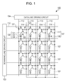
- Fig. 1 is an equivalent circuit view showing an electrical configuration of an organic EL apparatus
- Fig. 2 is a schematic plan view showing a configuration of an organic EL apparatus
- Fig. 3 is a schematic cross-sectional view showing a structure of a pixel of an organic EL apparatus
- Fig. 4 is a typical view showing a configuration of an organic EL element in a pixel of an organic EL apparatus.
- an organic EL apparatus 100 has a plurality of scanning lines 112 and a plurality of data lines 113 which are crossed each other, and power lines 114 in parallel with respect to each of a plurality of data lines 113.
- the organic EL apparatus 100 has a scanning line driving circuit 103 connected to a plurality of scanning lines 112 and a data line driving circuit 104 connected to a plurality of data lines 113.
- the organic EL apparatus 100 has a plurality of pixels 107 arranged in a matrix state corresponding to each crossing part of a plurality of scanning lines 112 and a plurality of data lines 113.
- the pixel 107 has an organic EL element 130 which is a luminescence element and a pixel circuit 111 controlling driving of the organic EL element 130.
- the organic EL element 130 is provided with a pixel electrode 131 as an anode, a counter electrode 134 as a cathode, and a functional layer 132 provided between the pixel electrode 131 and the counter electrode 134 and having a luminescence function.
- Such an organic EL element 130 can be represented as a diode, electrically. Description will be given of a detailed configuration of the functional layer 132 later, however, the functional layer 132 is configured of a plurality of thin film layers including the luminescence layer.
- the counter electrode 134 is formed as a common electrode over a plurality of pixels 107.
- the pixel circuit 111 includes a transistor for switch 121, a transistor for driving 122, and a storage capacitor 123.
- Two transistors 121 and 122 can be configured, for example, using an n-channel type or p-channel type thin film transistor (TFT), or a MOS transistor.
- a gate of the transistor for switch 121 is connected to the scanning line 112, one of a source or a drain of the transistor for switch 121 is connected to the data line 113, and the other of a source or a drain of the transistor for switch 121 is connected to a gate of the transistor for driving 122.
- One of a source or a drain of the transistor for driving 122 is connected to the pixel electrode 131 of the organic EL element 130 and the other of a source or a drain of the transistor for driving 122 is connected to the power line 114.
- the storage capacitor 123 is connected between the gate of the transistor for driving 122 and the power line 114.
- a potential based on an image signal supplied from the data line 113 at this time is retained in the storage capacitor 123 through the transistor for switch 121.
- An ON and OFF state of the transistor for driving 122 is determined in accordance with a potential of the storage capacitor 123, that is, a gate potential of the transistor for driving 122. Then, when the transistor for driving 122 turns to an ON state, a current having a magnitude in accordance with the gate potential flows from the power line 114 to the functional layer 132 sandwiched between the pixel electrode 131 and the counter electrode 134 through the transistor for driving 122.
- the organic EL element 130 produces luminescence in accordance with the magnitude of the current flowing through the functional layer 132.
- the configuration of the pixel circuit 111 is not limited thereto.
- a transistor for controlling luminescence by controlling the conduction between the transistor for driving 122 and the pixel electrode 131 may be provided between the transistor for driving 122 and the pixel electrode 131.
- the organic EL apparatus 100 has pixels 107R, 107G, and 107B in which the luminescence (the luminescence color) of red color (R), green color (G), and blue color (B) is obtained.
- Each of the pixels 107R, 107G, and 107B is in a substantially rectangular shape and is arranged in a matrix state in a display region E.
- the pixels 107R, 107G, and 107B are respectively provided with the organic EL element 130 (refer to Fig. 3 ) in which the luminescence of the corresponding colors is obtained.
- the pixels 107 in which the same luminescence colors are obtained are arrayed in a vertical direction (in a column direction or in a longitudinal direction of the pixel 107) on the drawing, and the pixels 107 of different luminescence colors are arrayed in the order of R, G, and B in a horizontal direction (in a row direction or in a short direction of the pixel 107) on the drawing. That is, the pixels 107R, 107G, and 107B of different luminescence colors are arranged in a so-called stripe system.
- the pixels 107R, 107G, and 107B of different luminescence colors are also sometimes collectively referred to as the pixel 107.
- a direction in which the pixels 107 of different luminescence colors are arrayed and a direction in which the pixels 107 of the same colors are arrayed are respectively set to an X direction and a Y direction to be explained.
- Such an organic EL apparatus 100 is used as a display apparatus, three pixels 107R, 107G, and 107B in which different luminescence colors are obtained are set to one display pixel unit 108 and the respective pixels 107R, 107G, and 107B are electrically controlled. Thereby, a full color display becomes possible.
- the planar shape and the arrangement of the pixels 107R, 107G, and 107B of different luminescence colors are not limited thereto and, for example, may be the arrangement of a delta system or a mosaic system.
- the pixels 107 are not limited to three colors of red color (R), green color (G), and blue color (B) and, for example, the luminescence of yellow color (Y) may be provided as well.
- the organic EL apparatus 100 has an organic EL element 130R in which the luminescence of red color is obtained, an organic EL element 130G in which the luminescence of green color is obtained, and an organic EL element 130B in which the luminescence of blue color is obtained, which are provided on an element substrate 101. That is, the organic EL element 130R is provided on the pixel 107R, the organic EL element 130G is provided on the pixel 107G, and the organic EL element 130B is provided on the pixel 107B.
- the respective organic EL elements 130R, 130G, and 130B has the pixel electrode 131 as an anode and the functional layer 132 including the luminescence layer formed on the pixel electrode 131.
- the respective organic EL elements 130R, 130G, and 130B have the counter electrode 134 as a common electrode formed to be opposed to the pixel electrode 131 through the functional layer 132.
- the pixel electrode 131 is sometimes referred to as the pixel electrodes 131R, 131G, and 131B corresponding to the luminescence colors.
- the functional layer 132 is sometimes referred to as the functional layers 132R, 132G, and 132B corresponding to the luminescence colors.
- the functional layers 132R, 132G, and 132B respectively include a plurality of thin film layers. At least one thin film layer among a plurality of thin film layers is formed using the ink for forming a functional layer described below by the liquid droplet discharging method (the ink jet method). Description will be given of a detailed configuration and method of forming of the functional layer 132 later.
- the pixel electrodes 131R, 131G, and 131B are respectively divided by a barrier wall 133 provided so as to cover a part of the periphery thereof.
- the barrier wall 133 is formed by using a photosensitive resin material having insulation properties such as, for example, a polyfunctional acrylic-based resin.
- the pixel electrode 131 is connected to one of three terminals of the transistor for driving 122 formed on the element substrate 101.
- a fixed potential such as, for example, GND is given to the counter electrode 134.
- holes are injected from the pixel electrode 131 into the functional layer 132 and electrons are injected from the counter electrode 134 into the functional layer 132.
- excitons are formed by the holes and the electrons injected, and when the excitons are disappeared (when the electrons and the holes are recombined), a part of the energy is released as fluorescence and phosphorescence.
- the organic EL apparatus 100 of the embodiment has a bottom emission type structure, and a light in which the luminescence is produced from the functional layers 132R, 132G, and 132B is reflected by the counter electrode 134 to be taken out from the element substrate 101 side. Therefore, a transparent substrate such as a glass is used as an element substrate 101.
- an opaque substrate for example, a thermosetting resin, a thermoplastic resin, and the like are included, in addition to one in which ceramics such as alumina or a metal sheet such as stainless steel is subjected to an insulation treatment such as surface oxidation.
- the pixel circuit 111 for driving the organic EL element 130 is provided in the element substrate 101. That is, a semiconductor layer 122a of the transistor for driving 122 is formed on a base insulating film 115 covering one surface of the element substrate 101.
- the semiconductor layer 122a consists of, for example, polysilicon.
- a gate insulating film 116 is formed so as to cover the semiconductor layer 122a.
- a region sandwiching the gate insulating film 116 and overlapping the gate electrode 126 is set to a channel region.
- the gate electrode 126 is electrically connected to the scanning line 112 (not shown).
- a first interlayer insulating film 117 is formed so as to cover the semiconductor layer 122a and the gate electrode 126.
- the semiconductor layer 122a while a low concentration source region and a high concentration source region 122c are provided on the source side of the channel region, a low concentration drain region and a high concentration drain region 122b are provided on the drain side of the channel region, that is, an LDD (Light Doped Drain) structure is formed.
- the high concentration source region 122c is connected to a source electrode 125 through a contact hole 125a which is opened over the gate insulating film 116 and the first interlayer insulating film 117.
- the source electrode 125 is configured as a part of the power line 114 (not shown).
- the high concentration drain region 122b is connected to a drain electrode 124 provided on the same wiring layer as that of the source electrode 125 through a contact hole 124a which is opened over the gate insulating film 116 and the first interlayer insulating film 117.
- a second interlayer insulating film 118 is formed on an upper layer of the first interlayer insulating film 117 on which the source electrode 125 and the drain electrode 124 are formed.
- the second interlayer insulating film 118 is formed in order to eliminate the unevenness on the surface due to the transistor for driving 122 or the like configuring the pixel circuit 111, the source electrode 125, the drain electrode 124, or the like, and is subjected to a flattening treatment such as CMP (Chemical Mechanical Polishing).
- the pixel electrode 131 is formed on the surface of the second interlayer insulating film 118 and is connected to the drain electrode 124 through a contact hole 118a provided on the second interlayer insulating film 118. That is, the pixel electrode 131 is connected to the high concentration drain region 122b of the semiconductor layer 122a through the drain electrode 124.
- the counter electrode 134 is connected to GND. Therefore, the driving current which is supplied from the power line 114 described above to the pixel electrode 131 by the transistor for driving 122 and flows between the pixel electrode 131 and the counter electrode 134 is controlled. Thereby, the pixel circuit 111 makes the desired organic EL elements 130R, 130G, and 130B produce luminescence and a color display becomes possible.
- the element substrate 101 having such an organic EL element 130 is fully sealed with the sealing substrate 102 without any space through the sealing layer 135 using a thermosetting type epoxy resin or the like as a sealing member.
- the organic EL element 130 of the organic EL apparatus 100 of the embodiment is manufactured by using a method of manufacturing described below and in forming the functional layers 132R, 132G, and 132B in which different luminescence colors are obtained, the particles (the foreign substances) to be mixed is respectively reduced, and thus the desired luminescent brightness and luminescent lifetimes are obtained.
- the organic EL apparatus 100 of the embodiment is not limited to bottom emission type and, for example, may be set to a top emission type structure in which the pixel electrode 131 is formed using a conductive material having light reflectivity, the counter electrode 134 as a cathode is formed using a transparent conductive material, and the luminescence from the organic EL element 130 is reflected by the pixel electrode 131 to be taken out from the sealing substrate 102 side.
- the organic EL apparatus 100 may also have a configuration in which color filters corresponding to the luminescence colors of the organic EL element 130 are provided corresponding to each of the organic EL elements 130R, 130G, and 130B.
- the organic EL apparatus 100 may also be set to a configuration in which white luminescence is obtained from the organic EL element 130.
- the organic EL apparatus 100 has the organic EL element 130R in which the luminescence of red color is obtained, the organic EL element 130G in which the luminescence of green color is obtained, and the organic EL element 130B in which the luminescence of blue color is obtained, which are provided on the element substrate 101.
- the organic EL element 130R in which the luminescence of red color is obtained has the pixel electrode 131R as an anode, the counter electrode 134 arranged opposite to the pixel electrode 131R as a cathode, a hole injection layer 132a, a hole transport layer 132b, a luminescence layer 132cR of red (R), a luminescence layer 132cB of blue (B), an electron transport layer 132d, and an electron injection layer 132e laminated from the pixel electrode 131R side in order between the pixel electrode 131R and the counter electrode 134.
- the organic EL element 130G in which the luminescence of green color is obtained has the pixel electrode 131G as an anode, the counter electrode 134 arranged opposite to the pixel electrode 131G as a cathode, the hole injection layer 132a, the hole transport layer 132b, a luminescence layer 132cG of green (G), the luminescence layer 132cB of blue (B), the electron transport layer 132d, and the electron injection layer 132e laminated from the pixel electrode 131G side in order between the pixel electrode 131G and the counter electrode 134.
- the organic EL element 130B in which the luminescence of blue color is obtained has the pixel electrode 131B as an anode, the counter electrode 134 arranged opposite to the pixel electrode 131B as a cathode, the hole injection layer 132a, the hole transport layer 132b, the luminescence layer 132cB of blue (B), the electron transport layer 132d, and the electron injection layer 132e laminated from the pixel electrode 131B side in order between the pixel electrode 131B and the counter electrode 134.
- the pixel electrodes 131R, 131G, and 131B are respectively formed using a transparent electrode material having a big work function such as, for example, ITO (Indium Tin Oxide) by the vapor phase process.
- ITO Indium Tin Oxide
- the counter electrode 134 is formed using an electrode material having a small work function such as, for example, Al as a cathode in common to the organic EL elements 130R, 130G, and 130B by the vapor phase process.
- the pixel electrodes 131R, 131G, and 131B are respectively divided by the barrier wall 133 which is subjected to a surface treatment.
- the hole injection layer 132a and the hole transport layer 132b are separately applied, serially, in order to be formed by the liquid phase process in the film forming region divided by the barrier wall 133 corresponding to each of the pixel electrodes 131R, 131G, and 131B.
- the luminescence layer 132cR is separately applied to be formed by the liquid phase process on the hole transport layer 132b corresponding to the pixel electrode 131R and the luminescence layer 132cG is separately applied to be formed by the liquid phase process on the hole transport layer 132b corresponding to the pixel electrode 131G.
- the luminescence layer 132cB of blue (B), the electron transport layer 132d, and the electron injection layer 132e are commonly formed over three organic EL elements 130R, 130G, and 130B by using the vapor phase process.
- the vapor phase process in the embodiment for example, is a vacuum deposition method.
- the liquid phase process for example, is a liquid droplet discharging method (an ink jet method).
- the luminescence layer 132cB of blue (B) commonly formed over three organic EL elements 130R, 130G, and 130B by using the vapor phase process is configured by including a host material having electron transport properties. Therefore, even if the luminescence layer 132cB of blue (B) is laminated on the luminescence layer 132cR of red (R), the luminescence of red color is obtained in the organic EL element 130R. In addition, even if the luminescence layer 132cB of blue (B) is laminated on luminescence layer 132cG of green (G), the luminescence of green color is obtained in the organic EL element 130G. The luminescence of blue color is naturally obtained from the organic EL element 130B having the luminescence layer 132cB of blue (B).
- other thin film layers may be formed for controlling the movement of carriers (the holes and the electrons) between the pixel electrodes 131R and 131G and the luminescence layers 132cR and 132cG, or between the luminescence layer 132cB and the counter electrode 134.
- one of the electron transport layer 132d and the electron injection layer 132e can also be removed, depending on a configuration of the counter electrode 134 or the luminescence layer 132cB as a cathode.
- the pixel electrodes 131R, 131G, and 131B as an anode are electrodes for injecting the holes into the hole injection layer 132a.
- a constituent material of these pixel electrodes 131R, 131G, and 131B is not particularly limited, however, a material having a big work function and excellent conductivity is suitably used, and, for example, a metallic oxide such as ITO (Indium Tin Oxide), IZO (Indium Zinc Oxide), In 2 O 3 , SnO 2 , fluorine-added SnO 2 , Sb-added SnO 2 , ZnO, Al-added ZnO, or Ga-added ZnO, Au, Pt, Ag, and Cu or an alloy including these, and the like are included and these can be used as one kind or in combination of two or more kinds thereof.
- a metallic oxide such as ITO (Indium Tin Oxide), IZO (Indium Zinc Oxide), In 2 O 3 , SnO 2 , fluorine-added SnO 2 , Sb-added SnO 2 , ZnO, Al-added ZnO, or Ga-added ZnO
- the film thickness of such pixel electrodes 131R, 131G, and 131B is not particularly limited, however, is preferably in a range from 10 nm to 200 nm and is more preferably in a range from 30 nm to 150 nm.
- the hole injection layer 132a is formed by applying a solution including a hole injection material (an ink for forming a functional layer) onto the predetermined film forming region, and then drying and heating the region (the liquid phase process).
- a hole injection material for example, a mixture (PEDOT:PSS) in which polystyrene sulfonate (PSS) as a dopant is added to a polythiophene derivative such as polyethylenedioxythiophene (PEDOT), polystyrene, polypyrrole, poly vinyl carbazole (PVK), polyaniline, oligoaniline, and polyacetylene or a derivative thereof, and the like are included.
- PEDOT polyethylenedioxythiophene
- PVK poly vinyl carbazole
- PEDOT polyethylenedioxythiophene
- oligoaniline oligoaniline
- polyacetylene or a derivative thereof, and the like are included.
- the film thickness of the hole injection layer 132a is not particularly limited, however, is preferably in a range from 10 nm to 150 nm.
- the hole transport layer 132b is provided between the hole injection layer 132a and the luminescence layers 132cR, 132cG, and 132cB in the organic EL elements 130R, 130G, and 130B, in order to improve transport properties (injection properties) of the holes to the luminescence layers 132cR, 132cG, and 132cB and suppress a decrease in function of the hole injection layer 132a due to the entering of electrons from the luminescence layers 132cR, 132cG, and 132cB into the hole injection layer 132a. That is, the hole transport layer 132b is for improving the luminescent efficiency owing to the combination of the holes and the electrons in the luminescence layers 132cR, 132cG, and 132cB.
- the hole transport layer 132b comes into contact with the hole injection layer 132a of the organic EL elements 130R, 130G, and 130B to be formed in common with the organic EL elements 130R, 130G, and 130B, by applying a solution including a hole transport material (an ink for forming a functional layer) onto the predetermined film forming region, and then drying and heating the region (the liquid phase process).
- a solution including a hole transport material an ink for forming a functional layer
- a hole transport material for example, a polymer of an amine-based compound such as triphenyldiamine (TPD) is suitably used.
- a high molecular organic material such as a polyfluorene derivative (PF), a polyparaphenylene vinylene derivative (PPV), a polyparaphenylene derivative (PPP), poly vinyl carbazole (PVK), a polythiophene derivative, or polysilane-based including poly methyl phenyl silane (PMPS) is included.
- the film thickness of the hole transport layer 132b is not particularly limited, however, is preferably in a range from 15 nm to 25 nm.
- the luminescence layer 132cR in which the luminescence of red color is obtained and the luminescence layer 132cG in which the luminescence of green color is obtained come into contact with the hole transport layer 132b of the organic EL elements 130R and 130G to be selectively formed corresponding to the organic EL elements 130R and 130G, respectively by applying a solution including a luminescence layer forming material in which the luminescence material as a guest material is doped in the host material(an ink for forming a functional layer) onto the predetermined film forming region, and then drying and heating the region (the liquid phase process).
- a low molecular material such as TDAPB (1,3,5-tris-(N,N-bis-(4-methoxy-phenyl)-amino phenyl)-benzene), CBP (4,4'-bis(9-dicarbazolyl)-2,2'-biphenyl), BAlq (bis-(2-methyl-8-quinolinolate)-4-(phenylphenolate)aluminum), mCP (N,N-dicarbazolyl-3,5-benzene: a CBP derivative), CDBP (4,4'-bis(9-carbazolyl)-2,2'-dimethyl-biphenyl), DCB (N,N'-dicarbazolyl-1,4-dimethene-benzene), P06 (2,7-bis(diphenylphosphineoxide)-9,9-dimethylfluorene), SimCP (3,5-bis(9-carbazolyl)tetrapheny
- TDAPB
- a fluorescence material and/or a phosphorescence material can be used.
- a fluorescence material ADS111RE (red color) and ADS108GE (green color) (poly[ ⁇ 9,9-dioctyl-2,7-divinylene-fluorenylene ⁇ -alt-co- ⁇ 2-methoxy-5-(2-ethylhexyloxy)-1,4-phenylene ⁇ ]) manufactured by American Dye Source, Inc. are included.
- an iridium complex such as Bt2Ir(acac) (bis(2-phenylbenxothiozolato-N,C2')iridium(III)(acetylacetonate)) or Btp2Ir(acac) (bis(2-(2'-benzothienyl)-pyridinato-N,C3)iridium(acetylacetonate)) and a platinum complex such as PtOEP (2,3,7,8,12,13,17,18-octaethyl-21H,23H-porphine, platinum (II)) are included, and it is possible to obtain the phosphorescence of red color by adding these to the host material described above.
- PtOEP 2,3,7,8,12,13,17,18-octaethyl-21H,23H-porphine, platinum (II)
- an iridium complex such as Ir(ppy)3 (fac-tris(2-phenypyridine)iridium) or Ppy2Ir(acac) (bis(2-phenyl-pyridinato-N,C2)iridium(acetylacetone)) is included, and it is possible to obtain the phosphorescence of green color by adding these to the host material described above.
- the film thickness of the luminescence layers 132cR and 132cG is not particularly limited, however, is preferably in a range from 5 nm to 100 nm and is more preferably in a range from 10 nm to 50 nm.
- the luminescence layer 132cB in which the luminescence of blue color is obtained is formed in common with the organic EL elements 130R, 130G, and 130B by doping the guest material (the luminescence material) in the low molecular host material having electron transport properties described above by the vapor phase process.
- the luminescence layer 132cB As a host material of the luminescence layer 132cB, it is preferable to use an anthracene derivative.
- a guest material (the luminescence material) of the luminescence layer 132cB a fluorescence material and/or a phosphorescence material can be used.
- a fluorescence material ADS136BE (blue color) manufactured by American Dye Source, Inc. is included.
- an iridium complex such as Flrpic (iridium-bis(4,6-difluorophenyl-pyridinato-N,C2)-picolinate), Ir(pmb)3 (iridium-tris(1-phenyl-3-methyl benzimidazolin-2-ylidene-C,C(2)')), FIrN4 (iridium(III)-bis(4,6-difluorophenylpyridinato)(5-(pyridin-2-yl)-tetrazolate)), or FIrtaz (iridium(III)bis(4,6-difluorophenylpyridinato)(5-(pyridine-2-yl)-1,2,4-triazolate)) is included, and it is possible to obtain the phosphorescence of blue color by adding these to the host material described above.
- Flrpic iridium-bis(4,6-difluorophenyl-pyridinato-N,
- the electron transport layer 132d is formed by using the vapour phase process and has a function of transporting the electrons injected from the counter electrode 134 as a cathode into the electron transport layer 132d to the luminescence layer 132cB.
- the electron transport layer 132d also has a function of blocking the holes passing through from the luminescence layer 132cB to the electron transport layer 132d in some cases.
- a electron transport material configuring the electron transport layer 132d is not particularly limited, however, for example, BALq, OXD-1 (1,3,5-tri-(5-(4-tert-butylphenyl)-1,3,4-oxadiazole)), BCP (bathocuproine), PBD (2-(4-biphenyl)-5-(4-tert-butylphenyl)-1,2,4-oxadiazole), TAZ (3-(4-biphenyl)-5-(4-tert-butylphenyl)-1,2,4-triazole), DPVBi (4,4'-bis(1,1-bis-diphenylethenyl)biphenyl), BND (2,5-bis(1-naphthyl)-1,3,4-oxadiazole), DTVBi (4,4'-bis(1,1-bis(4-methylphenyl)ethenyl)biphenyl), BBD (2,5-bis(4
- the film thickness of the electron transport layer 132d is not particularly limited, however, is preferably in a range from 1 nm to 100 nm and is more preferably in a range from 5 nm to 50 nm.
- the electron injection layer 132e is formed by using the vapor phase process and has a function of improving injection efficiency of the electrons from the counter electrode 134 into the electron transport layer 132d.
- a constituent material of the electron injection layer 132e is not particularly limited, however, for example, an alkali metal, an alkaline earth metal, or a compound of an alkali metal or an alkaline earth metal is included, and these can be used as one kind or in combination of two or more kinds thereof.
- alkali metal for example, Li, Na, K, Rb, and Cs are included.
- alkaline earth metal for example, Mg, Ca, Sr, and Ba are included.
- an alkali metal salt such as LiF, Li 2 CO 3 , LiCl, NaF, Na 2 CO 3 , NaCl, CsF, Cs 2 CO 3 , or CsCl is included.
- an alkaline earth metal salt such as CaF 2 , CaCO 3 , SrF 2 , SrCO 3 , BaF 2 , or BaCO 3 is included.
- the film thickness of the electron injection layer 132e is not particularly limited, however, is preferably in a range from 0.01 nm to 10 nm and more preferably in a range from 0.1nm to 5 nm.
- the counter electrode 134 as a cathode is an electrode for injecting the electrons into the electron injection layer 132e.
- a material having a small work function is used as a constituent material of the counter electrode 134.
- Li, Mg, Ca, Sr, La, Ce, Er, Eu, Sc, Y, Yb, Ag, Cu, Al, Cs, Rb, and Au or an alloy including these, or the like is used so as to be able to form the counter electrode 134 by using the vapour phase process such as a deposition method and these can be used as one kind or in a combination of two or more kinds thereof (for example, a laminated body having a plurality of layers or the like).
- a metal such as Al, Ag, AlAg, or AlNd or an alloy thereof is preferably used.
- a metal or alloy as a constituent material of the counter electrode 134, an improvement of the electron injection efficiency and stability of the counter electrode 134 can be achieved.
- the film thickness of the counter electrode 134 in the bottom emission structure is not particularly limited, however, for example, is preferably in a range from 50 nm to 1,000 nm and is more preferably in a range from 100 nm to 500 nm.
- a metal such as MgAg, MgAl, MgAu, and AlAg or an alloy thereof is preferably used, as a constituent material of the counter electrode 134.
- a metal or alloy as a constituent material of the counter electrode 134, while light transmitability of the counter electrode 134 is maintained, an improvement of the electron injection efficiency and stability of the counter electrode 134 can be achieved.
- the film thickness of the counter electrode 134 in the top emission structure is not particularly limited, however, for example, is preferably in a range from 1 nm to 50 nm and is more preferably in a range from 5 nm to 20 nm.
- the liquid droplet discharging method (the ink jet method) of discharging a solution (an ink for forming a functional layer) from a nozzle of an ink jet head as a droplet. It is possible to accurately discharge a solution with the predetermined amount into the desired film forming region as a droplet according to the liquid droplet discharging method (the ink jet method).
- a spin coating method (a pyrosol method), a casting method, a microgravure coating method, a gravure coating method, a bar coating method, a roll coating method, a wire bar coating method, a dip coating method, a spray coating method, a screen printing method, a flexo printing method, an offset printing method, and the like are included.
- a deposition method As a vapor phase process, a deposition method, a sputtering method, an ion beam method, and the like are included. It is preferable to use a deposition method in that heat or the like has hardly any effect on the film formed earlier when the film is formed.
- Figs. 5A to 5E and Figs. 6F to 6H are schematic cross-sectional views showing a method of manufacturing an organic EL element.
- the ink for forming a functional layer of the invention is applied to the method of manufacturing an organic EL element of the embodiment. Therefore, description will be given of an organic EL element 130R in which the hole injection layer 132a, the hole transport layer 132b, and the luminescence layer 132cR among the functional layers 132 are formed by the liquid phase process as an example. That is, Figs. 5A to 5E and Figs. 6F to 6H show a method of manufacturing the organic EL element 130R.
- an ink for forming a functional layer is referred to as simply "an ink" for convenience of explanation.
- the barrier wall 133 which covers the periphery (the part of the outer edge) of the pixel electrode 131R and divides a region provided with the pixel electrode 131R is formed (a barrier wall forming process).
- the region divided by the barrier wall 133 becomes the film forming region onto which an ink including the functional layer forming material is applied.
- a solution including, for example, a polyfunctional acrylic-based resin is applied and dried by a method such as a spin coating method so as to cover the surface of the element substrate 101 provided with the pixel electrode 131R and a photosensitive resin layer is formed. Afterward, a method of forming the barrier wall 133 by patterning the photosensitive resin layer by a photolithography method is included.
- the film forming region is subjected to the surface treatment so that the surface of the barrier wall 133 exhibits liquid repellency with respect to the ink and the surface of the pixel electrode 131R which is an example of an object to be discharged exhibits lyophilicity.
- the surface treatment As a method of the surface treatment, firstly, using oxygen as a treatment gas to carry out a plasma treatment, the surface of the pixel electrode 131R and the surface of the barrier wall 133 (including the surface of wall) are activated to be lyophilic. Subsequently, the plasma treatment is performed using a fluorine-based treatment gas such as CF 4 . Thereby, a method of selectively making the surface of the barrier wall 133 liquid repellent by reacting a fluorine-based treatment gas only on the surface of the barrier wall 133 consisting of an acrylic-based resin is included.
- a fluorine-based treatment gas such as CF 4
- the method of forming the barrier wall 133 in which the surface has liquid repellency is not limited thereto, and, for example, a method in which the barrier wall 133 is formed using a polyfunctional acrylic-based resin including a fluorine-based liquid repellency material may be employed.
- an ink 60 including the hole injection material is applied onto each film forming region divided by the barrier wall 133, as shown in Fig. 5B .
- the ink jet method (the liquid droplet discharging method) in which the ink 60 is discharged from a nozzle of the ink jet head 50 as a droplet, while the ink jet head 50 is arranged opposite and moves relative to the element substrate 101, is used.
- the applied ink 60 is filled into the film forming region divided by the barrier wall 133 and is raised by the interfacial surface tension.
- the applied ink 60 is heated and dried, for example, under an air atmosphere and the hole injection layer 132a coming into contact with the pixel electrode 131R is formed, as shown in Fig. 5C .
- the ink 60 with the predetermined amount as a droplet was discharged to the film forming region from the ink jet head 50 so that the film thickness of the hole injection layer 132a is approximately 130 nm after drying.
- the ink 60 is one, for example, in which poly vinyl carbazole (PVK), which is the hole injection material, is dissolved at a concentration of approximately 2.0 wt% in 3-phenoxytoluene as a solvent.
- PVK poly vinyl carbazole
- an ink 70 including the hole transport material is applied onto the film forming region divided by the barrier wall 133, as shown in Fig. 5D .
- the ink jet head 50 is also used for an application of the ink 70.
- a 3-phenoxytoluene solution including poly[(9,9-dioctylfluorenyl-2,7-diyl)-co-(4,4'-(N-(4-sec-butylphenyl))diphenylamine)] (TFB) in a concentration range from 1.5 wt% to 2.0 wt% as a hole transport material is used.
- the applied ink 70 is filled into the film forming region divided by the barrier wall 133 and is raised by the interfacial surface tension. Then, the applied ink 70 is heated and dried, for example, under a nitrogen atmosphere and the hole transport layer 132b coming into contact with the hole injection layer 132a is formed, as shown in Fig. 5E .
- the ink 70 with the predetermined amount as a droplet was discharged from the ink jet head 50 so that the film thickness of the hole transport layer 132b is approximately 20 nm after drying.
- an ink 80R including the luminescence layer forming material is applied onto the film forming region divided by the barrier wall 133, as shown in Fig. 6F .
- the ink jet head 50 is also used for an application of the ink 80R.
- the applied ink 80R is filled into the film forming region divided by the barrier wall 133 and is raised by the interfacial surface tension.
- the applied ink 80R for example, after decompression drying is performed at a vacuum degree of 5 Pa or less for 30 minutes, the applied ink 80R is dried at 130°C for 10 minutes under a nitrogen atmosphere using a drying machine (an oven) and the luminescence layer 132cR coming into contact with the hole transport layer 132b is formed, as shown in Fig. 6G .
- the applied ink 80R with the predetermined amount as a droplet was discharged from the ink jet head 50 so that the film thickness of the luminescence layer 132cR is approximately 45 nm after drying.
- the luminescence layer 132cB, the electron transport layer 132d, the electron injection layer 132e, and the counter electrode 134 as a cathode are formed by the vapor phase process.
- the films are sequentially formed using the materials of each layer described above, for example, by a vacuum deposition method and each layer is formed by laminating so as to cover the film forming region divided by the barrier wall 133 and the exposed surface of the barrier wall 133, as shown in Fig. 6H .
- the film may be formed using an inorganic material such as, for example, an oxide or nitride of silicon or an oxynitride of silicon having gas barrier properties so as to cover the surface of the counter electrode 134.
- an inorganic material such as, for example, an oxide or nitride of silicon or an oxynitride of silicon having gas barrier properties so as to cover the surface of the counter electrode 134.
- the method of manufacturing the organic EL element 130R is applied to a method of manufacturing the organic EL element 130G in the organic EL apparatus 100 and in the luminescence layer forming process, an ink 80G including the luminescence layer forming material (including the luminescence material in which the luminescence of green color is obtained and the host material) is used.
- the processes except the luminescence layer forming process are the same as those of the method of manufacturing the organic EL element 130R.
- the method of manufacturing the organic EL element 130R is applied to a method of manufacturing the organic EL element 130B in the organic EL apparatus 100, and in the luminescence layer forming process, the processes of forming each thin film layer of the hole injection layer 132a, the hole transport layer 132b, the electron transport layer 132d, the electron injection layer 132e, and the counter electrode 134 are the same as those of the method of manufacturing the organic EL element 130R except forming the luminescence layer 132cB by the vapor phase process.
- the ink for forming a functional layer of the invention is applied to the respective inks 60, 70, 80R, and 80G which are used, and the size and the number of the particles included in the ink for forming a functional layer are controlled.
- description will be given of an ink for forming a functional layer of the invention and a method of manufacturing the same with reference to Fig. 7 to Figs. 11A and 11B .
- Fig. 7 is a graph showing the relation between the size of a dark spot (DS) and the size of a foreign substance
- Fig. 8 is a table showing a proportion of an area which the size of a dark spot (DS) occupies in a pixel area.
- the organic EL element 130R has the functional layer 132R between the pixel electrode 131 and the counter electrode 134.
- the functional layer 132R includes the hole injection layer 132a, the hole transport layer 132b, the luminescence layer 132cR, the luminescence layer 132cB, the electron transport layer 132d, and the electron injection layer 132e.
- a range of the film thickness of the functional layer 132R is from 46 nm to 385 nm in view of a range of the film thickness of each thin film layer.
- the maximum value of the film thickness thereof is possibly approximately 500 nm (0.5 ⁇ m) or less, even with consideration of luminescence characteristics such as, for example, a driving voltage or luminescent lifetime.
- the bigger particles having conductivity the particles of a size of 0.5 ⁇ m or more having conductivity
- the film thickness of the functional layer 132R are mixed into the functional layer 132R, an electrical short circuit is generated between the pixel electrode 131 and the counter electrode 134, and thus the luminescence is not produced from the organic EL element 130R. That is, the pixel 107R including the organic EL element 130R becomes a defective pixel.
- the thing to be expected to avoid most is that the particles having conductivity is mixed into the ink for forming a functional layer.
- the part of which the particles exist becomes a dark spot (DS) in which luminescence is not produced.
- the inventors examined the relation between the size of the dark spot (DS) and the size of particles (foreign substances) which generate the dark spot (DS) by turning on a plurality of organic EL apparatuses 100 (samples) which are manufactured by way of trial to be observed. Moreover, “the size” described herein indicates a maximum diameter.
- the length of an opposite angle (that is, between opposite corners) in the display region E of the organic EL apparatus 100 which is manufactured by way of trial is approximately 3 inch and the number of pixels is 15,105.
- One display pixel unit 108 has three pixels 107 which are R, G, and B.
- the size of the luminescence region of the organic EL element 130 of one pixel 107 in a trial product is 27,197 ⁇ m 2 .
- the size of the dark spot (DS) is, for example, approximately 10 ⁇ m
- the size of the particles (the foreign substances) which are the cause thereof was approximately 3 ⁇ m at the smallest particles.
- the size of the dark spot (DS) is approximately 25 ⁇ m
- the size of the particles (the foreign substances) which are the cause thereof was approximately 6 ⁇ m at the smallest particles.
- the size of the particles (the foreign substances) which are the cause of the dark spot (DS) is from 1/3.5 to 1/8 of the size of the dark spot (DS). That is, since the configuration of the thin film layer is not proper not only on the part of which the particles (the foreign substances) exist, but also on the periphery thereof, the region in which the luminescence is not normally produced exists. Moreover, in a graph shown in Fig. 7 , an inclination of an approximation primary straight line showing the correlation is approximately 0.33.
- the relation between the size of the dark spot (DS) and the size of the particles (the foreign substances) was examined, after removing the dark spot (DS) including the particles (the foreign substances) having a size of 20 ⁇ m or more which were mixed clearly from environmental sources during manufacturing the trial products.
- the proportion of a decrease in brightness of the pixel 107 is in proportion to the proportion of an area of the dark spot (DS) occupying in an area of the pixel 107.
- a pixel area becomes, for example, 11,729 ⁇ m 2 .
- the proportion of an area in which the dark spot (DS) having a size of 4 ⁇ m ⁇ (12.6 ⁇ m 2 ) occupies becomes 0.11%.
- the proportion of an area in which the dark spot (DS) having a size of 10 ⁇ m ⁇ (78.5 ⁇ m 2 ) occupies becomes 0.67% and the proportion of an area in which the dark spot (DS) having a size of 20 ⁇ m ⁇ (314 ⁇ m 2 ) occupies becomes 2.68%.
- one pixel area becomes, for example, 6,840 ⁇ m 2 even with the same number of pixels of 4K2K.
- the proportion of an area in which the dark spot (DS) having a size of 4 ⁇ m ⁇ (12.6 ⁇ m 2 ) occupies becomes 0.18%.
- the proportion of an area in which the dark spot (DS) having a size of 10 ⁇ m ⁇ (78.5 ⁇ m 2 ) occupies becomes 1.15% and the proportion of an area in which the dark spot (DS) having a size of 20 ⁇ m ⁇ (314 ⁇ m 2 ) occupies becomes 4.59%.
- one pixel area becomes, for example, 2,932 ⁇ m 2 .
- the proportion of an area in which the dark spot (DS) having a size of 4 ⁇ m ⁇ (12.6 ⁇ m 2 ) occupies becomes 0.43%.
- the proportion of an area in which the dark spot (DS) having a size of 10 ⁇ m ⁇ (78.5 ⁇ m 2 ) occupies becomes 2.68% and the proportion of an area in which the dark spot (DS) having a size of 20 ⁇ m ⁇ (314 ⁇ m 2 ) occupies becomes 10.71%.
- the allowable size of the dark spot (DS) is approximately 18.6 ⁇ m ⁇ . In doing so, the allowable size of the foreign substances which are the cause of the dark spot (DS) becomes 2.3 ⁇ m when fitting 1/8 as describe above. In the same way, in a case where the pixel area is 11,729 ⁇ m 2 , the allowable size of the dark spot (DS) is approximately 12.2 ⁇ m ⁇ and the allowable size of the foreign substances becomes 1.5 ⁇ m. In a case where the pixel area is 6,840 ⁇ m 2 , the allowable size of the dark spot (DS) is approximately 9.3 ⁇ m ⁇ and the allowable size of the foreign substances becomes 1.2 ⁇ m. In a case where the pixel area is 2,932 ⁇ m 2 , the allowable size of the dark spot (DS) is approximately 6.1 ⁇ m ⁇ and the allowable size of the foreign substances becomes 0.8 ⁇ m (refer to Fig. 8 ).
- the size of the pixel is arbitrarily set depending on the product design, it is preferable to reduce the particles included in the ink for forming a functional layer which is used as much as possible in a case where at least one layer of the thin film layer among the functional layers 132 of the organic EL element 130 provided on the pixel 107 is formed by the liquid phase process.
- a method of removing fine particles from the ink for forming a functional layer a method of filtering the ink for forming a functional layer using a filter requires time and labor and has an effect on productivity in a manufacturing process.
- an in-liquid particle counter (KS-42BF) manufactured by RION Co., Ltd. was used.
- This in-liquid particle counter employs a light scattering system in which the particle diameter and the number of the particles are determined by irradiating with a light beam intersecting to a transparent passage (a flow cell) in a sensor, generating a pulse from a scattered light quantity produced by the particles passing through an irradiation region, and analyzing a pulse height.
- the minimum diameter of the particles capable of being detected is 0.2 ⁇ m.
- a sample passes through the passage (the flow cell) at a speed of 10 ml/minute. The measurement was performed two to four times and the average value of measurement was set to a result of measurement.
- Fig. 9A is a graph showing a result of measurement of particles in an ink for forming a functional layer after dilution
- Fig. 9B is a graph showing a result of measurement of particles in acetone which is a solvent used for dilution.
- the result of measurement of the particles shown in Fig. 9A is a result in which the number of the particles before dilution is estimated based on a result in which a sample diluted to 100 times with acetone was measured using the in-liquid particle counter.
- the luminescence layer forming material as a functional layer forming material was dissolved in 3-phenoxytoluene as a solvent so that the concentration of the luminescence layer forming material was 1.0 wt%.
- this result of measurement is a result including the particles in acetone used for dilution.
- 1,350 particles having a particle diameter of 0.2 ⁇ m or more, 308 particles having a particle diameter of 0.3 ⁇ m or more, 121 particles having a particle diameter of 0.4 ⁇ m or more, 61 particles having a particle diameter of 0.5 ⁇ m or more, 13 particles having a particle diameter of 1.0 ⁇ m or more, 6 particles having a particle diameter of 1.5 ⁇ m or more, and 3 particles having a particle diameter of 2.0 ⁇ m or more were included in 10 ml of acetone at EL grade. Therefore, the number of the foreign substances included in acetone (EL grade) used for dilution is a level which can be ignored, compared to the number of the particles included in the ink for forming a functional layer after dilution.
- Fig. 10 is a graph showing a result of measurement of particles after an ink for forming a functional layer is filtered using a filter having a hole diameter of 0.2 ⁇ m.
- an in-liquid particle counter KS-42A manufactured by RION Co., Ltd. was used in the measurement of the particles in the ink for forming a functional layer after filtering. The minimum diameter in which the in-liquid particle counter KS-42A can detect is 0.1 ⁇ m.
- the filter used for filtration in the embodiment is a capsule type filter provided with a mesh filter having a predetermined hole diameter.
- a mesh filter for example, PFA (tetrafluoroethylene and perfluoroalkyl vinyl ether copolymer) or PTFE (polytetrafluoroethylene) which is a fluorine-based resin, PP (polypropylene), PE (polyethylene), and the like are included.
- the hole diameter of the mesh filter can be selected in accordance with the particle diameter of the particles to be filtered.
- the ink for forming a functional layer is filtered by pressure-injecting into the capsule type filter.
- Fig. 10 The results of measurement of the particles after filtering the ink for forming a functional layer using the filter having a hole diameter of 0.2 ⁇ m are shown in Fig. 10 .
- 110 ml of the ink for forming a functional layer was filtered by the filter, the ink for forming a functional layer after filtering was set to a sample, and the measurement was performed by using the in-liquid particle counter KS-42A described above.
- Fig. 10 The results of measurement of the particles after filtering the ink for forming a functional layer using the filter having a hole diameter of 0.2 ⁇ m are shown in Fig. 10 .
- 110 ml of the ink for forming a functional layer was filtered by the filter, the ink for forming a functional layer after filtering was set to a sample, and the measurement was performed by using the in-liquid particle counter KS-42A described above.
- KS-42A the in-liquid particle counter
- a plurality of organic EL apparatuses 100 were manufactured by way of trial using the ink for forming a functional layer after filtering with the filter having a hole diameter of 0.2 ⁇ m and an occurrence status of the dark spot (DS) was verified.
- a plurality of organic EL elements 130R were formed using the ink for forming a functional layer after filtering and the relation between an occurrence status of the dark spot (DS) and the particles (the foreign substances) was examined.
- the area (the area of the luminescence region) of the film forming region of the organic EL element 130 in the organic EL apparatus 100 (the number of pixels is 15,105) of the trial product is approximately 27,197 ⁇ m 2 .
- the ink 60 for forming the hole injection layer, the ink 70 for forming the hole transport layer, and the ink 80R for forming the luminescence layer, which are used for forming one organic EL element 130R based on the method of manufacturing the organic EL element described above, are respectively 420 ng, 384 ng, and 297 ng, and the total becomes 1,101 ng. Therefore, the total amount of ink used for forming a plurality of the organic EL elements 130R is 1,101 ng ⁇ 15,105 ⁇ 16.6 mg, that is, approximately 16 ml.
- the particles which does not become the dark spot (DS), for example, which are generated due to not completely dissolving the functional layer forming material in a solvent exist in the particles having a particle diameter of 0.5 ⁇ m or more measured by the in-liquid particle counter.
- the particles which can become the dark spot (DS) indicate the solid content which is an impurity included in the ink for forming a functional layer and is not dissolved in a solvent.
- Figs. 11A and 11B The results of measurement are shown in Figs. 11A and 11B.
- Fig. 11A is a graph showing a result of measurement of particles after the ink for forming a functional layer is filtered twice using the filter having a hole diameter of 0.05 ⁇ m
- Fig. 11B is a graph showing a result of measurement of particles after filtering 20 times.
- the average value of measurements taken several times was displayed to one decimal place.
- DS unallowable dark spot
- the number of the unallowable dark spot (DS) that is, the number of the defective pixel becomes less than 5 by setting the number of the particles of 0.5 ⁇ m or more in 10 ml of the ink for forming a functional layer to 7 or less, it is considered as a level that can be accepted as a quality assurance level in manufacturing the actual product.
- 165. 3 particles having a particle diameter of 0.2 ⁇ m or more, 48.7 particles having a particle diameter of 0.3 ⁇ m or more, 13 particles having a particle diameter of 0.4 ⁇ m or more, 5 particles having a particle diameter of 0.5 ⁇ m or more, 2 particles having a particle diameter of 1.0 ⁇ m or more, and 1.7 particles having a particle diameter of 1.5 ⁇ m were included in the ink for forming a functional layer after filtering 20 times using the filter having a hole diameter of 0.05 ⁇ m.
- the number of the defective pixels in which a decrease in brightness is recognized is recognized to less than 5
- the probability in which the foreign substances are redundantly included in the same pixel 107 is practically, considerably low in consideration with a response to the finer pixel size (for example, the number of pixels is 8K4K) or forming, for example, the hole injection layer 132a or the hole transport layer 132b other than the luminescence layer among the functional layers 132 consisting of a plurality of thin film layers by the liquid phase process, it is more preferable to set the number of the particles having a particle diameter of 0.5 ⁇ m or more included in 10 ml of the ink for forming a functional layer to less than 1.
- Such a method of manufacturing the ink for forming a functional layer has a first process of measuring the size and the number of the particles included in the ink for forming a functional layer after mixing (before filtering) per unit volume (10 ml), a second process of selecting a hole diameter of a filter based on a result of the first process, and the third process of filtering the ink for forming a functional layer using the filter having a hole diameter selected in the second process. Then, in the second process, it is preferable to select the hole diameter of the filter from the relation between the hole diameter of the filter and the number of the particles having a size of 0.5 ⁇ m or more after filtering.
- the hole diameter of the filter and the number of times of filtration so that the number of particles of 0.5 ⁇ m or more is 7 or less in 10 ml of the ink for forming a functional layer after filtering. Furthermore, it is more preferable to determine the hole diameter of the filter and the number of times of filtration so that the number of particles of 0.5 ⁇ m or more is less than 1 in 10 ml of the ink for forming a functional layer after filtering.
- the ink for forming a functional layer in which the size and the number of the particles are controlled.
- the filtration may repeatedly be performed by using the filters having the same hole diameter or the filtration may repeatedly be performed while reducing the hole diameter step by step by using the filters having different hole diameters. It is preferable to filter with the filter having a bigger hole diameter first and then to filter by switching to the filter having a smaller hole diameter in consideration with the time taken to filter.
- the ink for forming a functional layer is discharged from the ink jet head 50 as a droplet
- the organic EL element to which the ink for forming a functional layer of the invention can be applied is not limited to one having the luminescence layer 132cR (or the luminescence layer 132cG) and the luminescence layer 132cB between the pixel electrode 131 as an anode and the counter electrode 134 as a cathode.
- the luminescence layer formed by the liquid phase process may be one layer or at least one layer of thin film layer among a plurality of thin film layers configuring the functional layer 132 may be formed using the ink for forming a functional layer.
- An element in which the ink for forming a functional layer of the invention and the method of manufacturing the same can be applied is not limited to the organic EL element.
- a microoptical element such as an organic semiconductor element, a structure of MEMS, or microlense, and the like are included.
- the configuration of the functional layer forming material included in the ink for forming a functional layer or the solvent for dissolving the functional layer forming material is not limited to the configurations of the inks 60, 70, 80G, and 80R as the ink for forming a functional layer described above.
- the ink for forming a functional layer is applied using the ink jet head 50 (in a case where the liquid droplet discharging method is used)
- the viscosity of the ink for forming a functional layer be 30 mPa ⁇ s (second) or less.
Landscapes
- Chemical & Material Sciences (AREA)
- Engineering & Computer Science (AREA)
- Life Sciences & Earth Sciences (AREA)
- Materials Engineering (AREA)
- Wood Science & Technology (AREA)
- Organic Chemistry (AREA)
- Manufacturing & Machinery (AREA)
- Electroluminescent Light Sources (AREA)
Abstract
Description
- The present invention relates to an ink for forming a functional layer, a method of manufacturing an ink for forming a functional layer, and a method of manufacturing an organic electro-luminescence element.
- As a method of forming a functional layer by using a solution including a functional layer forming material as an ink and applying the solution onto a film forming region to be solidified, a liquid droplet discharging method using an ink jet head capable of discharging an ink from a nozzle as a droplet is employed. By using the liquid droplet discharging method, it is possible to accurately arrange an ink with a required amount as a droplet in the film forming region and form a stable functional layer in a film shape.
- As an example of the functional layer formed by such a liquid droplet discharging method, a wiring layer, a semiconductive layer, a coloring layer in a color filter, a luminescence layer in a luminescence element, and the like are included.
- When foreign substances (particles) are included in the solution (ink) including the functional layer forming material, the functional layer is formed in a state in which the foreign substances (the particles) are included in the film forming region, and thus a part in which an original function can not be obtained in the functional layer is generated.
- Therefore, for example, in
JP-A-2007-95516 - In addition, for example, in
JP-A-2013-26164 JP-A-2013-26164 - However, in a display apparatus having an electrically independent organic electro-luminescence element for each pixel, even if one layer among the organic luminescence medium layers is formed using the application liquid in
JP-A-2007-95516 JP-A-2013-26164 - The invention can be realized in the following forms or application examples. Application Example
- According to an application example, there is provided an ink for forming a functional layer, which is used when any thin film layer among functional layers consisting of a plurality of thin film layers is formed, including a functional layer forming material and a solvent for dissolving the functional layer forming material, and in which the number of particles of 0.5 µm or more is 7 or less in 10 ml of the ink for forming a functional layer.
- According to the application example, since the size and the number of particles are controlled, if this ink for forming a functional layer is used, it is possible to form the thin film layer in good yield.
- Moreover, as a method of specifying the size and the number of particles included in a liquid, a method using an in-liquid particle counter is included and it is considered that at least 10 ml is required as a volume of a sample in order to accurately measure. That is, it is preferable to specify the size and the number of particles by setting 10 ml to a unit.
- In the ink for forming a functional layer described in the application example, it is preferable that the number of particles of 0.5 µm or more be less than 1 in 10 ml of the ink.
- According to this configuration, even if a region on which the ink for forming a functional layer is applied is small, it is possible to form the thin film layer in which the occurrence of a defect is reduced.
- According to this application example, there is provided a method of manufacturing an ink for forming a functional layer which is used when any thin film layer among functional layers consisting of a plurality of thin film layers is formed, including measuring the size and the number of particles included in the ink for forming a functional layer per unit volume after mixing, selecting a hole diameter of a filter based on a result of the measuring, and filtering the ink for forming a functional layer using a filter having a hole diameter selected in the selecting, in which, in the selecting, a hole diameter of a filter is selected from a relation between a hole diameter of a filter and the number of particles having a size of 0.5 µm or more after filtering.
- According to the application example, it is possible to manufacture the ink for forming a functional layer in which the size and the number of particles are properly controlled.
- In the method of manufacturing an ink for forming a functional layer described in the application example described above, in the selecting, it is preferable to determine the hole diameter of the filter and the number of times of filtration so that the number of particles of 0.5 µm or more is 7 or less in 10 ml of the ink after filtering.
- According to this method, it is possible to manufacture the ink for forming a functional layer in which the occurrence of a defect is further reduced.
- According to the application example, there is provided a method of manufacturing an organic electro-luminescence element provided with a functional layer consisting of a plurality of thin film layers between an anode and a cathode and having a luminescence function, including forming any thin film layer among the functional layers using the ink for forming a functional layer described in the application example described above.
- According to this application example, there is provided a method of manufacturing an organic electro-luminescence element provided with a functional layer consisting of a plurality of thin film layers between an anode and a cathode and having a luminescence function, including forming any thin film layer among the functional layers using an ink for forming a functional layer manufactured by the method of manufacturing the ink for forming a functional layer described in the application example described above.
- According to these application examples, it is possible to reduce the occurrence of a defect resulting from the particles and manufacture the organic electro-luminescence element in good yield.
- Embodiments of the invention will now be described by way of example only with reference to the accompanying drawings, wherein like numbers reference like elements.
-
Fig. 1 is an equivalent circuit view showing an electrical configuration of an organic EL apparatus. -
Fig. 2 is a schematic plan view showing a configuration of an organic EL apparatus. -
Fig. 3 is a schematic cross-sectional view showing a structure of a pixel of an organic EL apparatus. -
Fig. 4 is a typical view showing a configuration of an organic EL element in a pixel of an organic EL apparatus. -
Figs. 5A to 5E are schematic cross-sectional views showing a method of manufacturing an organic EL element. -
Figs. 6F to 6H are schematic cross-sectional views showing a method of manufacturing an organic EL element. -
Fig. 7 is a graph showing the relation between the size of a dark spot (DS) and the size of a foreign substance. -
Fig. 8 is a table showing a proportion of an area in which the size of a dark spot (DS) occupies in a pixel area. -
Fig. 9A is a graph showing a result of measurement of particles in an ink for forming a functional layer after dilution andFig. 9B is a graph showing a result of measurement of particles in acetone which is a solvent used for dilution. -
Fig. 10 is a graph showing a result of measurement of particles after an ink for forming a functional layer is filtered using a filter having a hole diameter of 0.2 µm. -
Fig. 11A is a graph showing a result of measurement of particles after an ink for forming a functional layer is filtered twice using a filter having a hole diameter of 0.05 µm andFig. 11B is a graph showing a result of measurement of particles after filtering 20 times. - Hereinafter, description will be given of an embodiment in which the invention is embodied in accordance with drawings. Moreover, the used drawings are displayed by appropriately enlarging or reducing the size so as to become a state in which parts of description can be recognized.
- Moreover, in the following aspects, for example, in a case where "on a substrate" is described, a case of arranging so as to contact on a substrate, a case of arranging on a substrate through another component, or a case of arranging so as to partially contact on a substrate and partially arranging on a substrate through another component is indicated.
- First, description will be given of an example of an organic electro-luminescence (EL) apparatus which is a self-luminous type display apparatus provided with an organic EL element in a pixel with reference to
Fig. 1 to Fig. 4 .Fig. 1 is an equivalent circuit view showing an electrical configuration of an organic EL apparatus,Fig. 2 is a schematic plan view showing a configuration of an organic EL apparatus,Fig. 3 is a schematic cross-sectional view showing a structure of a pixel of an organic EL apparatus, andFig. 4 is a typical view showing a configuration of an organic EL element in a pixel of an organic EL apparatus. - As shown in
Fig. 1 , anorganic EL apparatus 100 has a plurality ofscanning lines 112 and a plurality ofdata lines 113 which are crossed each other, andpower lines 114 in parallel with respect to each of a plurality ofdata lines 113. Theorganic EL apparatus 100 has a scanningline driving circuit 103 connected to a plurality ofscanning lines 112 and a dataline driving circuit 104 connected to a plurality ofdata lines 113. In addition, theorganic EL apparatus 100 has a plurality ofpixels 107 arranged in a matrix state corresponding to each crossing part of a plurality ofscanning lines 112 and a plurality ofdata lines 113. - The
pixel 107 has anorganic EL element 130 which is a luminescence element and apixel circuit 111 controlling driving of theorganic EL element 130. - The
organic EL element 130 is provided with apixel electrode 131 as an anode, acounter electrode 134 as a cathode, and afunctional layer 132 provided between thepixel electrode 131 and thecounter electrode 134 and having a luminescence function. Such anorganic EL element 130 can be represented as a diode, electrically. Description will be given of a detailed configuration of thefunctional layer 132 later, however, thefunctional layer 132 is configured of a plurality of thin film layers including the luminescence layer. Moreover, thecounter electrode 134 is formed as a common electrode over a plurality ofpixels 107. - The
pixel circuit 111 includes a transistor forswitch 121, a transistor for driving 122, and astorage capacitor 123. Twotransistors - A gate of the transistor for
switch 121 is connected to thescanning line 112, one of a source or a drain of the transistor forswitch 121 is connected to thedata line 113, and the other of a source or a drain of the transistor forswitch 121 is connected to a gate of the transistor for driving 122. - One of a source or a drain of the transistor for driving 122 is connected to the
pixel electrode 131 of theorganic EL element 130 and the other of a source or a drain of the transistor for driving 122 is connected to thepower line 114. Thestorage capacitor 123 is connected between the gate of the transistor for driving 122 and thepower line 114. - When the
scanning line 112 is driven and the transistor forswitch 121 turns to an ON state, a potential based on an image signal supplied from thedata line 113 at this time is retained in thestorage capacitor 123 through the transistor forswitch 121. An ON and OFF state of the transistor for driving 122 is determined in accordance with a potential of thestorage capacitor 123, that is, a gate potential of the transistor for driving 122. Then, when the transistor for driving 122 turns to an ON state, a current having a magnitude in accordance with the gate potential flows from thepower line 114 to thefunctional layer 132 sandwiched between thepixel electrode 131 and thecounter electrode 134 through the transistor for driving 122. Theorganic EL element 130 produces luminescence in accordance with the magnitude of the current flowing through thefunctional layer 132. - Moreover, the configuration of the
pixel circuit 111 is not limited thereto. For example, a transistor for controlling luminescence by controlling the conduction between the transistor for driving 122 and thepixel electrode 131 may be provided between the transistor for driving 122 and thepixel electrode 131. - As shown in
Fig. 2 , theorganic EL apparatus 100 haspixels pixels E. The pixels Fig. 3 ) in which the luminescence of the corresponding colors is obtained. Thepixels 107 in which the same luminescence colors are obtained are arrayed in a vertical direction (in a column direction or in a longitudinal direction of the pixel 107) on the drawing, and thepixels 107 of different luminescence colors are arrayed in the order of R, G, and B in a horizontal direction (in a row direction or in a short direction of the pixel 107) on the drawing. That is, thepixels - Hereinafter, the
pixels pixel 107. In addition, a direction in which thepixels 107 of different luminescence colors are arrayed and a direction in which thepixels 107 of the same colors are arrayed are respectively set to an X direction and a Y direction to be explained. - If such an
organic EL apparatus 100 is used as a display apparatus, threepixels display pixel unit 108 and therespective pixels - Moreover, the planar shape and the arrangement of the
pixels pixels 107 are not limited to three colors of red color (R), green color (G), and blue color (B) and, for example, the luminescence of yellow color (Y) may be provided as well. - As shown in
Fig. 3 , theorganic EL apparatus 100 has anorganic EL element 130R in which the luminescence of red color is obtained, anorganic EL element 130G in which the luminescence of green color is obtained, and anorganic EL element 130B in which the luminescence of blue color is obtained, which are provided on anelement substrate 101. That is, theorganic EL element 130R is provided on thepixel 107R, theorganic EL element 130G is provided on thepixel 107G, and theorganic EL element 130B is provided on thepixel 107B. The respectiveorganic EL elements pixel electrode 131 as an anode and thefunctional layer 132 including the luminescence layer formed on thepixel electrode 131. In addition, the respectiveorganic EL elements counter electrode 134 as a common electrode formed to be opposed to thepixel electrode 131 through thefunctional layer 132. - The
pixel electrode 131 is sometimes referred to as thepixel electrodes functional layer 132 is sometimes referred to as thefunctional layers functional layers functional layer 132 later. - The
pixel electrodes barrier wall 133 provided so as to cover a part of the periphery thereof. Thebarrier wall 133 is formed by using a photosensitive resin material having insulation properties such as, for example, a polyfunctional acrylic-based resin. - The
pixel electrode 131 is connected to one of three terminals of the transistor for driving 122 formed on theelement substrate 101. A fixed potential, such as, for example, GND is given to thecounter electrode 134. By applying a driving potential between thepixel electrode 131 and thecounter electrode 134, holes are injected from thepixel electrode 131 into thefunctional layer 132 and electrons are injected from thecounter electrode 134 into thefunctional layer 132. In the luminescence layer included in thefunctional layer 132, excitons are formed by the holes and the electrons injected, and when the excitons are disappeared (when the electrons and the holes are recombined), a part of the energy is released as fluorescence and phosphorescence. - The
organic EL apparatus 100 of the embodiment has a bottom emission type structure, and a light in which the luminescence is produced from thefunctional layers counter electrode 134 to be taken out from theelement substrate 101 side. Therefore, a transparent substrate such as a glass is used as anelement substrate 101. In addition, for a sealingsubstrate 102 arranged opposite to theelement substrate 101 through asealing layer 135, either a transparent substrate or an opaque substrate can be used. As an opaque substrate, for example, a thermosetting resin, a thermoplastic resin, and the like are included, in addition to one in which ceramics such as alumina or a metal sheet such as stainless steel is subjected to an insulation treatment such as surface oxidation. - In the
element substrate 101, thepixel circuit 111 for driving theorganic EL element 130 is provided. That is, asemiconductor layer 122a of the transistor for driving 122 is formed on abase insulating film 115 covering one surface of theelement substrate 101. Thesemiconductor layer 122a consists of, for example, polysilicon. Agate insulating film 116 is formed so as to cover thesemiconductor layer 122a. - In addition, in the
semiconductor layer 122a, a region sandwiching thegate insulating film 116 and overlapping thegate electrode 126 is set to a channel region. Moreover, thegate electrode 126 is electrically connected to the scanning line 112 (not shown). A firstinterlayer insulating film 117 is formed so as to cover thesemiconductor layer 122a and thegate electrode 126. - In addition, in the
semiconductor layer 122a, while a low concentration source region and a highconcentration source region 122c are provided on the source side of the channel region, a low concentration drain region and a highconcentration drain region 122b are provided on the drain side of the channel region, that is, an LDD (Light Doped Drain) structure is formed. Among those, the highconcentration source region 122c is connected to asource electrode 125 through acontact hole 125a which is opened over thegate insulating film 116 and the firstinterlayer insulating film 117. Thesource electrode 125 is configured as a part of the power line 114 (not shown). On the other hand, the highconcentration drain region 122b is connected to adrain electrode 124 provided on the same wiring layer as that of thesource electrode 125 through acontact hole 124a which is opened over thegate insulating film 116 and the firstinterlayer insulating film 117. - A second
interlayer insulating film 118 is formed on an upper layer of the firstinterlayer insulating film 117 on which thesource electrode 125 and thedrain electrode 124 are formed. The secondinterlayer insulating film 118 is formed in order to eliminate the unevenness on the surface due to the transistor for driving 122 or the like configuring thepixel circuit 111, thesource electrode 125, thedrain electrode 124, or the like, and is subjected to a flattening treatment such as CMP (Chemical Mechanical Polishing). - Then, the
pixel electrode 131 is formed on the surface of the secondinterlayer insulating film 118 and is connected to thedrain electrode 124 through acontact hole 118a provided on the secondinterlayer insulating film 118. That is, thepixel electrode 131 is connected to the highconcentration drain region 122b of thesemiconductor layer 122a through thedrain electrode 124. Thecounter electrode 134 is connected to GND. Therefore, the driving current which is supplied from thepower line 114 described above to thepixel electrode 131 by the transistor for driving 122 and flows between thepixel electrode 131 and thecounter electrode 134 is controlled. Thereby, thepixel circuit 111 makes the desiredorganic EL elements - The
element substrate 101 having such anorganic EL element 130 is fully sealed with the sealingsubstrate 102 without any space through thesealing layer 135 using a thermosetting type epoxy resin or the like as a sealing member. - The
organic EL element 130 of theorganic EL apparatus 100 of the embodiment is manufactured by using a method of manufacturing described below and in forming thefunctional layers - Moreover, the
organic EL apparatus 100 of the embodiment is not limited to bottom emission type and, for example, may be set to a top emission type structure in which thepixel electrode 131 is formed using a conductive material having light reflectivity, thecounter electrode 134 as a cathode is formed using a transparent conductive material, and the luminescence from theorganic EL element 130 is reflected by thepixel electrode 131 to be taken out from the sealingsubstrate 102 side. In addition, in a case of having top emission type, theorganic EL apparatus 100 may also have a configuration in which color filters corresponding to the luminescence colors of theorganic EL element 130 are provided corresponding to each of theorganic EL elements organic EL apparatus 100 has a color filter, theorganic EL apparatus 100 may also be set to a configuration in which white luminescence is obtained from theorganic EL element 130. - Next, description will be given of a specific configuration of the
organic EL elements Fig. 4 . - As shown in
Fig. 4 , theorganic EL apparatus 100 has theorganic EL element 130R in which the luminescence of red color is obtained, theorganic EL element 130G in which the luminescence of green color is obtained, and theorganic EL element 130B in which the luminescence of blue color is obtained, which are provided on theelement substrate 101. - The
organic EL element 130R in which the luminescence of red color is obtained has thepixel electrode 131R as an anode, thecounter electrode 134 arranged opposite to thepixel electrode 131R as a cathode, ahole injection layer 132a, ahole transport layer 132b, a luminescence layer 132cR of red (R), a luminescence layer 132cB of blue (B), anelectron transport layer 132d, and anelectron injection layer 132e laminated from thepixel electrode 131R side in order between thepixel electrode 131R and thecounter electrode 134. - The
organic EL element 130G in which the luminescence of green color is obtained has thepixel electrode 131G as an anode, thecounter electrode 134 arranged opposite to thepixel electrode 131G as a cathode, thehole injection layer 132a, thehole transport layer 132b, a luminescence layer 132cG of green (G), the luminescence layer 132cB of blue (B), theelectron transport layer 132d, and theelectron injection layer 132e laminated from thepixel electrode 131G side in order between thepixel electrode 131G and thecounter electrode 134. - The
organic EL element 130B in which the luminescence of blue color is obtained has thepixel electrode 131B as an anode, thecounter electrode 134 arranged opposite to thepixel electrode 131B as a cathode, thehole injection layer 132a, thehole transport layer 132b, the luminescence layer 132cB of blue (B), theelectron transport layer 132d, and theelectron injection layer 132e laminated from thepixel electrode 131B side in order between thepixel electrode 131B and thecounter electrode 134. - The
pixel electrodes - The
counter electrode 134 is formed using an electrode material having a small work function such as, for example, Al as a cathode in common to theorganic EL elements - Though an illustration is omitted in
Fig. 4 , thepixel electrodes barrier wall 133 which is subjected to a surface treatment. Thehole injection layer 132a and thehole transport layer 132b are separately applied, serially, in order to be formed by the liquid phase process in the film forming region divided by thebarrier wall 133 corresponding to each of thepixel electrodes hole transport layer 132b corresponding to thepixel electrode 131R and the luminescence layer 132cG is separately applied to be formed by the liquid phase process on thehole transport layer 132b corresponding to thepixel electrode 131G. - On the other hand, the luminescence layer 132cB of blue (B), the
electron transport layer 132d, and theelectron injection layer 132e are commonly formed over threeorganic EL elements - The luminescence layer 132cB of blue (B) commonly formed over three
organic EL elements organic EL element 130R. In addition, even if the luminescence layer 132cB of blue (B) is laminated on luminescence layer 132cG of green (G), the luminescence of green color is obtained in theorganic EL element 130G. The luminescence of blue color is naturally obtained from theorganic EL element 130B having the luminescence layer 132cB of blue (B). - Moreover, other thin film layers may be formed for controlling the movement of carriers (the holes and the electrons) between the
pixel electrodes counter electrode 134. In addition, one of theelectron transport layer 132d and theelectron injection layer 132e can also be removed, depending on a configuration of thecounter electrode 134 or the luminescence layer 132cB as a cathode. - Hereinafter, more specifically, description will be give of a configuration of the
organic EL elements - The
pixel electrodes hole injection layer 132a. - A constituent material of these
pixel electrodes - The film thickness of
such pixel electrodes - The
hole injection layer 132a is formed by applying a solution including a hole injection material (an ink for forming a functional layer) onto the predetermined film forming region, and then drying and heating the region (the liquid phase process). As a hole injection material, for example, a mixture (PEDOT:PSS) in which polystyrene sulfonate (PSS) as a dopant is added to a polythiophene derivative such as polyethylenedioxythiophene (PEDOT), polystyrene, polypyrrole, poly vinyl carbazole (PVK), polyaniline, oligoaniline, and polyacetylene or a derivative thereof, and the like are included. - The film thickness of the
hole injection layer 132a is not particularly limited, however, is preferably in a range from 10 nm to 150 nm. - The
hole transport layer 132b is provided between thehole injection layer 132a and the luminescence layers 132cR, 132cG, and 132cB in theorganic EL elements hole injection layer 132a due to the entering of electrons from the luminescence layers 132cR, 132cG, and 132cB into thehole injection layer 132a. That is, thehole transport layer 132b is for improving the luminescent efficiency owing to the combination of the holes and the electrons in the luminescence layers 132cR, 132cG, and 132cB. - The
hole transport layer 132b comes into contact with thehole injection layer 132a of theorganic EL elements organic EL elements - As a hole transport material, for example, a polymer of an amine-based compound such as triphenyldiamine (TPD) is suitably used. In addition, a high molecular organic material such as a polyfluorene derivative (PF), a polyparaphenylene vinylene derivative (PPV), a polyparaphenylene derivative (PPP), poly vinyl carbazole (PVK), a polythiophene derivative, or polysilane-based including poly methyl phenyl silane (PMPS) is included.
- The film thickness of the
hole transport layer 132b is not particularly limited, however, is preferably in a range from 15 nm to 25 nm. - The luminescence layer 132cR in which the luminescence of red color is obtained and the luminescence layer 132cG in which the luminescence of green color is obtained come into contact with the
hole transport layer 132b of theorganic EL elements organic EL elements - As a host material, a low molecular material such as TDAPB (1,3,5-tris-(N,N-bis-(4-methoxy-phenyl)-amino phenyl)-benzene), CBP (4,4'-bis(9-dicarbazolyl)-2,2'-biphenyl), BAlq (bis-(2-methyl-8-quinolinolate)-4-(phenylphenolate)aluminum), mCP (N,N-dicarbazolyl-3,5-benzene: a CBP derivative), CDBP (4,4'-bis(9-carbazolyl)-2,2'-dimethyl-biphenyl), DCB (N,N'-dicarbazolyl-1,4-dimethene-benzene), P06 (2,7-bis(diphenylphosphineoxide)-9,9-dimethylfluorene), SimCP (3,5-bis(9-carbazolyl)tetraphenylsilane), or UGH3 (w-bis(triphenylsilyl)benzene) is included. Any of these low molecular host materials have electron transport properties.
- As a luminescence material, a fluorescence material and/or a phosphorescence material can be used. As a fluorescence material, ADS111RE (red color) and ADS108GE (green color) (poly[{9,9-dioctyl-2,7-divinylene-fluorenylene}-alt-co-{2-methoxy-5-(2-ethylhexyloxy)-1,4-phenylene}]) manufactured by American Dye Source, Inc. are included.
- As a phosphorescence material, an iridium complex such as Bt2Ir(acac) (bis(2-phenylbenxothiozolato-N,C2')iridium(III)(acetylacetonate)) or Btp2Ir(acac) (bis(2-(2'-benzothienyl)-pyridinato-N,C3)iridium(acetylacetonate)) and a platinum complex such as PtOEP (2,3,7,8,12,13,17,18-octaethyl-21H,23H-porphine, platinum (II)) are included, and it is possible to obtain the phosphorescence of red color by adding these to the host material described above.
- In addition, an iridium complex such as Ir(ppy)3 (fac-tris(2-phenypyridine)iridium) or Ppy2Ir(acac) (bis(2-phenyl-pyridinato-N,C2)iridium(acetylacetone)) is included, and it is possible to obtain the phosphorescence of green color by adding these to the host material described above.
- The film thickness of the luminescence layers 132cR and 132cG is not particularly limited, however, is preferably in a range from 5 nm to 100 nm and is more preferably in a range from 10 nm to 50 nm.
- The luminescence layer 132cB in which the luminescence of blue color is obtained is formed in common with the
organic EL elements - As a host material of the luminescence layer 132cB, it is preferable to use an anthracene derivative. In addition, as a guest material (the luminescence material) of the luminescence layer 132cB, a fluorescence material and/or a phosphorescence material can be used. As a fluorescence material, ADS136BE (blue color) manufactured by American Dye Source, Inc. is included.
- As a phosphorescence material, an iridium complex such as Flrpic (iridium-bis(4,6-difluorophenyl-pyridinato-N,C2)-picolinate), Ir(pmb)3 (iridium-tris(1-phenyl-3-methyl benzimidazolin-2-ylidene-C,C(2)')), FIrN4 (iridium(III)-bis(4,6-difluorophenylpyridinato)(5-(pyridin-2-yl)-tetrazolate)), or FIrtaz (iridium(III)bis(4,6-difluorophenylpyridinato)(5-(pyridine-2-yl)-1,2,4-triazolate)) is included, and it is possible to obtain the phosphorescence of blue color by adding these to the host material described above.
- The
electron transport layer 132d is formed by using the vapour phase process and has a function of transporting the electrons injected from thecounter electrode 134 as a cathode into theelectron transport layer 132d to the luminescence layer 132cB. In addition, theelectron transport layer 132d also has a function of blocking the holes passing through from the luminescence layer 132cB to theelectron transport layer 132d in some cases. - A electron transport material configuring the
electron transport layer 132d is not particularly limited, however, for example, BALq, OXD-1 (1,3,5-tri-(5-(4-tert-butylphenyl)-1,3,4-oxadiazole)), BCP (bathocuproine), PBD (2-(4-biphenyl)-5-(4-tert-butylphenyl)-1,2,4-oxadiazole), TAZ (3-(4-biphenyl)-5-(4-tert-butylphenyl)-1,2,4-triazole), DPVBi (4,4'-bis(1,1-bis-diphenylethenyl)biphenyl), BND (2,5-bis(1-naphthyl)-1,3,4-oxadiazole), DTVBi (4,4'-bis(1,1-bis(4-methylphenyl)ethenyl)biphenyl), BBD (2,5-bis(4-biphenylyl)-1,3,4-oxadiazole), and the like are included so as to be able to form theelectron transport layer 132d by using the vapour phase process such as a deposition method. - In addition, tris(8-quinolinolato)aluminium (Alq3), an oxadiazole derivative, an oxazole derivative, a phenanthroline derivative, an anthraquinodimethane derivative, a benzoquinone derivative, a naphthoquinone derivative, an anthraquinone derivative, a tetracyanoanthraquinodimethane derivative, a fluorene derivative, a diphenyldicyanoethylene derivative, a diphenoquinone derivative, a hydroxy quinoline derivative, and the like are included. These can be used as one kind or in combination of two or more thereof.
- The film thickness of the
electron transport layer 132d is not particularly limited, however, is preferably in a range from 1 nm to 100 nm and is more preferably in a range from 5 nm to 50 nm. - The
electron injection layer 132e is formed by using the vapor phase process and has a function of improving injection efficiency of the electrons from thecounter electrode 134 into theelectron transport layer 132d. - A constituent material of the
electron injection layer 132e (an electron injection material) is not particularly limited, however, for example, an alkali metal, an alkaline earth metal, or a compound of an alkali metal or an alkaline earth metal is included, and these can be used as one kind or in combination of two or more kinds thereof. - As an alkali metal, for example, Li, Na, K, Rb, and Cs are included. In addition, as an alkaline earth metal, for example, Mg, Ca, Sr, and Ba are included.
- As a compound of an alkali metal, for example, an alkali metal salt such as LiF, Li2CO3, LiCl, NaF, Na2CO3, NaCl, CsF, Cs2CO3, or CsCl is included. In addition, as a compound of an alkaline earth metal, for example, an alkaline earth metal salt such as CaF2, CaCO3, SrF2, SrCO3, BaF2, or BaCO3 is included.
- The film thickness of the
electron injection layer 132e is not particularly limited, however, is preferably in a range from 0.01 nm to 10 nm and more preferably in a range from 0.1nm to 5 nm. - The
counter electrode 134 as a cathode is an electrode for injecting the electrons into theelectron injection layer 132e. - It is preferable to use a material having a small work function as a constituent material of the
counter electrode 134. In addition, for example, Li, Mg, Ca, Sr, La, Ce, Er, Eu, Sc, Y, Yb, Ag, Cu, Al, Cs, Rb, and Au or an alloy including these, or the like is used so as to be able to form thecounter electrode 134 by using the vapour phase process such as a deposition method and these can be used as one kind or in a combination of two or more kinds thereof (for example, a laminated body having a plurality of layers or the like). - In particular, in a case of setting to the
organic EL apparatus 100 having the bottom emission structure as the embodiment, light transmitability is not required for thecounter electrode 134 and as a constituent material of thecounter electrode 134, for example, a metal such as Al, Ag, AlAg, or AlNd or an alloy thereof is preferably used. By using such a metal or alloy as a constituent material of thecounter electrode 134, an improvement of the electron injection efficiency and stability of thecounter electrode 134 can be achieved. - The film thickness of the
counter electrode 134 in the bottom emission structure is not particularly limited, however, for example, is preferably in a range from 50 nm to 1,000 nm and is more preferably in a range from 100 nm to 500 nm. - In a case where the
organic EL apparatus 100 is set to the top emission structure, for example, a metal such as MgAg, MgAl, MgAu, and AlAg or an alloy thereof is preferably used, as a constituent material of thecounter electrode 134. By using such a metal or alloy as a constituent material of thecounter electrode 134, while light transmitability of thecounter electrode 134 is maintained, an improvement of the electron injection efficiency and stability of thecounter electrode 134 can be achieved. - The film thickness of the
counter electrode 134 in the top emission structure is not particularly limited, however, for example, is preferably in a range from 1 nm to 50 nm and is more preferably in a range from 5 nm to 20 nm. - As a liquid phase process used when forming the
hole injection layer 132a, thehole transport layer 132b, and the luminescence layers 132cR and 132cG included in thefunctional layer - As a vapor phase process, a deposition method, a sputtering method, an ion beam method, and the like are included. It is preferable to use a deposition method in that heat or the like has hardly any effect on the film formed earlier when the film is formed.
- Next, description will be given of a method of manufacturing an organic EL element of the embodiment with reference to
Figs. 5A to 5E andFigs. 6F to 6H .Figs. 5A to 5E andFigs. 6F to 6H are schematic cross-sectional views showing a method of manufacturing an organic EL element. The ink for forming a functional layer of the invention is applied to the method of manufacturing an organic EL element of the embodiment. Therefore, description will be given of anorganic EL element 130R in which thehole injection layer 132a, thehole transport layer 132b, and the luminescence layer 132cR among thefunctional layers 132 are formed by the liquid phase process as an example. That is,Figs. 5A to 5E andFigs. 6F to 6H show a method of manufacturing theorganic EL element 130R. Hereinafter, an ink for forming a functional layer is referred to as simply "an ink" for convenience of explanation. - Firstly, as shown in
Fig. 5A , thebarrier wall 133 which covers the periphery (the part of the outer edge) of thepixel electrode 131R and divides a region provided with thepixel electrode 131R is formed (a barrier wall forming process). The region divided by thebarrier wall 133 becomes the film forming region onto which an ink including the functional layer forming material is applied. - As a specific method of forming the
barrier wall 133, a solution including, for example, a polyfunctional acrylic-based resin is applied and dried by a method such as a spin coating method so as to cover the surface of theelement substrate 101 provided with thepixel electrode 131R and a photosensitive resin layer is formed. Afterward, a method of forming thebarrier wall 133 by patterning the photosensitive resin layer by a photolithography method is included. - Since the ink is applied onto the film forming region including the
pixel electrode 131R in the latter process, the film forming region is subjected to the surface treatment so that the surface of thebarrier wall 133 exhibits liquid repellency with respect to the ink and the surface of thepixel electrode 131R which is an example of an object to be discharged exhibits lyophilicity. - As a method of the surface treatment, firstly, using oxygen as a treatment gas to carry out a plasma treatment, the surface of the
pixel electrode 131R and the surface of the barrier wall 133 (including the surface of wall) are activated to be lyophilic. Subsequently, the plasma treatment is performed using a fluorine-based treatment gas such as CF4. Thereby, a method of selectively making the surface of thebarrier wall 133 liquid repellent by reacting a fluorine-based treatment gas only on the surface of thebarrier wall 133 consisting of an acrylic-based resin is included. - Moreover, the method of forming the
barrier wall 133 in which the surface has liquid repellency is not limited thereto, and, for example, a method in which thebarrier wall 133 is formed using a polyfunctional acrylic-based resin including a fluorine-based liquid repellency material may be employed. - Next, in the hole injection layer forming process, an
ink 60 including the hole injection material is applied onto each film forming region divided by thebarrier wall 133, as shown inFig. 5B . For an application of theink 60, the ink jet method (the liquid droplet discharging method) in which theink 60 is discharged from a nozzle of theink jet head 50 as a droplet, while theink jet head 50 is arranged opposite and moves relative to theelement substrate 101, is used. The appliedink 60 is filled into the film forming region divided by thebarrier wall 133 and is raised by the interfacial surface tension. Then, the appliedink 60 is heated and dried, for example, under an air atmosphere and thehole injection layer 132a coming into contact with thepixel electrode 131R is formed, as shown inFig. 5C . In addition, in the embodiment, theink 60 with the predetermined amount as a droplet was discharged to the film forming region from theink jet head 50 so that the film thickness of thehole injection layer 132a is approximately 130 nm after drying. - The
ink 60 is one, for example, in which poly vinyl carbazole (PVK), which is the hole injection material, is dissolved at a concentration of approximately 2.0 wt% in 3-phenoxytoluene as a solvent. - Next, in the hole transport layer forming process, an
ink 70 including the hole transport material is applied onto the film forming region divided by thebarrier wall 133, as shown inFig. 5D . Theink jet head 50 is also used for an application of theink 70. For theink 70, for example, a 3-phenoxytoluene solution including poly[(9,9-dioctylfluorenyl-2,7-diyl)-co-(4,4'-(N-(4-sec-butylphenyl))diphenylamine)] (TFB) in a concentration range from 1.5 wt% to 2.0 wt% as a hole transport material is used. The appliedink 70 is filled into the film forming region divided by thebarrier wall 133 and is raised by the interfacial surface tension. Then, the appliedink 70 is heated and dried, for example, under a nitrogen atmosphere and thehole transport layer 132b coming into contact with thehole injection layer 132a is formed, as shown inFig. 5E . Theink 70 with the predetermined amount as a droplet was discharged from theink jet head 50 so that the film thickness of thehole transport layer 132b is approximately 20 nm after drying. - Next, in the luminescence layer forming process, an
ink 80R including the luminescence layer forming material is applied onto the film forming region divided by thebarrier wall 133, as shown inFig. 6F . Theink jet head 50 is also used for an application of theink 80R. For theink 80R, for example, a 3-phenoxytoluene solution including the luminescence layer forming material at a concentration from 1.0 wt% to 2.0 wt%, formed by adding the luminescence material in which the luminescence of red color is obtained to the host material described above, is used. The appliedink 80R is filled into the film forming region divided by thebarrier wall 133 and is raised by the interfacial surface tension. Then, as to the appliedink 80R, for example, after decompression drying is performed at a vacuum degree of 5 Pa or less for 30 minutes, the appliedink 80R is dried at 130°C for 10 minutes under a nitrogen atmosphere using a drying machine (an oven) and the luminescence layer 132cR coming into contact with thehole transport layer 132b is formed, as shown inFig. 6G . The appliedink 80R with the predetermined amount as a droplet was discharged from theink jet head 50 so that the film thickness of the luminescence layer 132cR is approximately 45 nm after drying. - Next, the luminescence layer 132cB, the
electron transport layer 132d, theelectron injection layer 132e, and thecounter electrode 134 as a cathode are formed by the vapor phase process. Specifically, the films are sequentially formed using the materials of each layer described above, for example, by a vacuum deposition method and each layer is formed by laminating so as to cover the film forming region divided by thebarrier wall 133 and the exposed surface of thebarrier wall 133, as shown inFig. 6H . In particular, it is preferable to form thecounter electrode 134 by a vacuum deposition method in that a damage of thefunctional layer 132 by heat can be prevented. In addition, in order to prevent a decrease in luminescence function or luminescent lifetime of thefunctional layer 132 due to water or a gas such as oxygen entering into thefunctional layer 132 from outside, the film may be formed using an inorganic material such as, for example, an oxide or nitride of silicon or an oxynitride of silicon having gas barrier properties so as to cover the surface of thecounter electrode 134. Thereby, theorganic EL element 130R having excellent luminescent characteristics (luminescent brightness, luminescent lifetime, or the like) is produced. - Moreover, the method of manufacturing the
organic EL element 130R is applied to a method of manufacturing theorganic EL element 130G in theorganic EL apparatus 100 and in the luminescence layer forming process, an ink 80G including the luminescence layer forming material (including the luminescence material in which the luminescence of green color is obtained and the host material) is used. The processes except the luminescence layer forming process are the same as those of the method of manufacturing theorganic EL element 130R. In addition, the method of manufacturing theorganic EL element 130R is applied to a method of manufacturing theorganic EL element 130B in theorganic EL apparatus 100, and in the luminescence layer forming process, the processes of forming each thin film layer of thehole injection layer 132a, thehole transport layer 132b, theelectron transport layer 132d, theelectron injection layer 132e, and thecounter electrode 134 are the same as those of the method of manufacturing theorganic EL element 130R except forming the luminescence layer 132cB by the vapor phase process. - In the process of manufacturing the
organic EL elements respective inks Fig. 7 to Figs. 11A and11B . -
Fig. 7 is a graph showing the relation between the size of a dark spot (DS) and the size of a foreign substance, andFig. 8 is a table showing a proportion of an area which the size of a dark spot (DS) occupies in a pixel area. - Firstly, description will be given of the relation between particles (foreign substances) included in an ink for forming a functional layer and a dark spot (DS) with reference to
Fig. 7 to Fig. 8 . - For example, the
organic EL element 130R has thefunctional layer 132R between thepixel electrode 131 and thecounter electrode 134. Thefunctional layer 132R includes thehole injection layer 132a, thehole transport layer 132b, the luminescence layer 132cR, the luminescence layer 132cB, theelectron transport layer 132d, and theelectron injection layer 132e. As described above, a range of the film thickness of thefunctional layer 132R is from 46 nm to 385 nm in view of a range of the film thickness of each thin film layer. Even if thefunctional layer 132R includes a thin film layer other than the thin film layers described above, the maximum value of the film thickness thereof is possibly approximately 500 nm (0.5 µm) or less, even with consideration of luminescence characteristics such as, for example, a driving voltage or luminescent lifetime. For example, when the bigger particles having conductivity (the particles of a size of 0.5 µm or more having conductivity) than the film thickness of thefunctional layer 132R are mixed into thefunctional layer 132R, an electrical short circuit is generated between thepixel electrode 131 and thecounter electrode 134, and thus the luminescence is not produced from theorganic EL element 130R. That is, thepixel 107R including theorganic EL element 130R becomes a defective pixel. In addition, when theorganic EL element 130R is electrically short circuited and an excess current starts to flow, it becomes difficult to flow enough current to theorganic EL element 130R which is short circuited and anotherorganic EL element 130 expected to produce luminescence at the same time, and thus there is a risk to occur luminescence unevenness. Therefore, the thing to be expected to avoid most is that the particles having conductivity is mixed into the ink for forming a functional layer. - On the other hand, even if the particles included in the ink for forming a functional layer has insulation properties, the current does not flow into the
functional layer 132R at a part of which the particles exist, therefore, the part of which the particles exist becomes a dark spot (DS) in which luminescence is not produced. - Therefore, the inventors examined the relation between the size of the dark spot (DS) and the size of particles (foreign substances) which generate the dark spot (DS) by turning on a plurality of organic EL apparatuses 100 (samples) which are manufactured by way of trial to be observed. Moreover, "the size" described herein indicates a maximum diameter.
- The length of an opposite angle (that is, between opposite corners) in the display region E of the
organic EL apparatus 100 which is manufactured by way of trial is approximately 3 inch and the number of pixels is 15,105. Onedisplay pixel unit 108 has threepixels 107 which are R, G, and B. The size of the luminescence region of theorganic EL element 130 of onepixel 107 in a trial product (approximately, equivalent to the size of the film forming region) is 27,197 µm2. - As a result of truing on a plurality of
organic EL elements 130R of the trial products to be confirmed, it was confirmed that there was a correlation between the size of the dark spot (DS) and the size of the particles (the foreign substances), as shown inFig. 7 . Specifically, when the size of the dark spot (DS) is, for example, approximately 10 µm, the size of the particles (the foreign substances) which are the cause thereof was approximately 3 µm at the smallest particles. In addition, when the size of the dark spot (DS) is approximately 25 µm, the size of the particles (the foreign substances) which are the cause thereof was approximately 6 µm at the smallest particles. The size of the particles (the foreign substances) which are the cause of the dark spot (DS) is from 1/3.5 to 1/8 of the size of the dark spot (DS). That is, since the configuration of the thin film layer is not proper not only on the part of which the particles (the foreign substances) exist, but also on the periphery thereof, the region in which the luminescence is not normally produced exists. Moreover, in a graph shown inFig. 7 , an inclination of an approximation primary straight line showing the correlation is approximately 0.33. In addition, the relation between the size of the dark spot (DS) and the size of the particles (the foreign substances) was examined, after removing the dark spot (DS) including the particles (the foreign substances) having a size of 20 µm or more which were mixed clearly from environmental sources during manufacturing the trial products. - On the other hand, whether the
pixel 107 having the dark spot (DS) practically becomes a defective pixel or not depends on how much the brightness of thepixel 107 decreases due to the dark spot (DS) with respect to the predetermined value. Even if the dark spot (DS) is included, if the proportion of a decrease in brightness is small, it is difficult to visually confirm, and thus it is not determined as a defective pixel. It is considered that the proportion of a decrease in brightness of thepixel 107 is in proportion to the proportion of an area of the dark spot (DS) occupying in an area of thepixel 107. - As shown in
Fig. 8 , for example, when the length of an opposite angle in the display region E in the panel specification of theorganic EL apparatus 100 is set to 55 inch and the number of pixels is set to 3,840x2,160=8,294,400 (hereinafter, this number of pixels is referred to as 4K2K), one pixel area becomes, for example, 11,729 µm2. In this pixel area, for example, the proportion of an area in which the dark spot (DS) having a size of 4 µmϕ (12.6 µm2) occupies becomes 0.11%. In the same way, the proportion of an area in which the dark spot (DS) having a size of 10 µmϕ (78.5 µm2) occupies becomes 0.67% and the proportion of an area in which the dark spot (DS) having a size of 20 µmϕ (314 µm2) occupies becomes 2.68%. - In addition, for example, when the length of an opposite angle in the display region E in the panel specification is set to 42 inch, one pixel area becomes, for example, 6,840 µm2 even with the same number of pixels of 4K2K. In this pixel area, for example, the proportion of an area in which the dark spot (DS) having a size of 4 µmϕ (12.6 µm2) occupies becomes 0.18%. In the same way, the proportion of an area in which the dark spot (DS) having a size of 10 µmϕ (78.5 µm2) occupies becomes 1.15% and the proportion of an area in which the dark spot (DS) having a size of 20 µmϕ (314 µm2) occupies becomes 4.59%.
- In addition, for example, when the length of an opposite angle in the display region E in the panel specification is set to 55 inch and the number of pixels is set to 7,680x4,320=33,177,600 (hereinafter, this number of pixels is referred to as 8K4K), one pixel area becomes, for example, 2,932 µm2. In this pixel area, for example, the proportion of an area in which the dark spot (DS) having a size of 4 µmϕ (12.6 µm2) occupies becomes 0.43%. In the same way, the proportion of an area in which the dark spot (DS) having a size of 10 µmϕ (78.5 µm2) occupies becomes 2.68% and the proportion of an area in which the dark spot (DS) having a size of 20 µmϕ (314 µm2) occupies becomes 10.71%.
- As described above, whether determined as a defective pixel or not depends on the area (the size) of the dark spot (DS) occupying in the pixel area described above. When the inventors observed the dark spots (DS) by the pixel areas, it was confirmed that a decrease in brightness in the pixel was recognized when the area (the size) of the dark spot (DS) occupying in the pixel area described above exceeded 1.0%.
- Therefore, in a case where the pixel area is 27,197 µm2, the allowable size of the dark spot (DS) is approximately 18.6 µmϕ. In doing so, the allowable size of the foreign substances which are the cause of the dark spot (DS) becomes 2.3 µm when fitting 1/8 as describe above. In the same way, in a case where the pixel area is 11,729 µm2, the allowable size of the dark spot (DS) is approximately 12.2 µmϕ and the allowable size of the foreign substances becomes 1.5 µm. In a case where the pixel area is 6,840 µm2, the allowable size of the dark spot (DS) is approximately 9.3 µmϕ and the allowable size of the foreign substances becomes 1.2 µm. In a case where the pixel area is 2,932 µm2, the allowable size of the dark spot (DS) is approximately 6.1 µmϕ and the allowable size of the foreign substances becomes 0.8 µm (refer to
Fig. 8 ). - Since the size of the pixel is arbitrarily set depending on the product design, it is preferable to reduce the particles included in the ink for forming a functional layer which is used as much as possible in a case where at least one layer of the thin film layer among the
functional layers 132 of theorganic EL element 130 provided on thepixel 107 is formed by the liquid phase process. On the other hand, as a method of removing fine particles from the ink for forming a functional layer, a method of filtering the ink for forming a functional layer using a filter requires time and labor and has an effect on productivity in a manufacturing process. - From the correlation between the size of the dark spot (DS) and the actual size of the particles (the foreign substances) showing in
Fig. 7 , even in a case where the number of pixels is 8K4K described above, it is necessary to control the number of the particles of 0.8 µm or more in which the size of the dark spot (DS) becomes approximately 6.0 µm or more so that the particles (the foreign substances) in the ink for forming a functional layer do not lead to a defective pixel (a pixel in which a decrease in brightness is recognized). Since the pixel area is a design item, when a margin is taken into consideration, it is preferable to control the number of the particles of 0.5 µm or more in which the size of the dark spot (DS) becomes approximately 4.0 µm or more. In other words, the control of the number of the particles having a size less than 0.5 µm need not be set so strictly. - Therefore, the measurement of the particles included in the ink for forming a functional layer after mixing (before filtering) was attempted. In the measurement of the particles, an in-liquid particle counter (KS-42BF) manufactured by RION Co., Ltd. was used. This in-liquid particle counter employs a light scattering system in which the particle diameter and the number of the particles are determined by irradiating with a light beam intersecting to a transparent passage (a flow cell) in a sensor, generating a pulse from a scattered light quantity produced by the particles passing through an irradiation region, and analyzing a pulse height. The minimum diameter of the particles capable of being detected is 0.2 µm. For the measurement, a sample passes through the passage (the flow cell) at a speed of 10 ml/minute. The measurement was performed two to four times and the average value of measurement was set to a result of measurement.
- Since it is considered that a considerable amount of particles is included in the ink for forming a functional layer after mixing (before filtering), it is not proper that the measurement of an undiluted solution is performed by using the in-liquid particle counter which is a light scattering system. Therefore, not an undiluted solution but a solution in which an undiluted solution was diluted with a solvent was set to a sample. Specifically, one in which the undiluted solution was diluted by 100 times using acetone at EL grade (electronic material grade) manufactured by Kanto Chemical Co., Inc. as a solvent was set to a sample.
-
Fig. 9A is a graph showing a result of measurement of particles in an ink for forming a functional layer after dilution andFig. 9B is a graph showing a result of measurement of particles in acetone which is a solvent used for dilution. - The result of measurement of the particles shown in
Fig. 9A is a result in which the number of the particles before dilution is estimated based on a result in which a sample diluted to 100 times with acetone was measured using the in-liquid particle counter. To form the sample before dilution the luminescence layer forming material as a functional layer forming material was dissolved in 3-phenoxytoluene as a solvent so that the concentration of the luminescence layer forming material was 1.0 wt%. - According to the result of measurement (the estimated value) in
Fig. 9A , 48,985,417 particles having a particle diameter of 0.2 µm or more, 11,175,000 particles having a particle diameter of 0.3 µm or more, 804,167 particles having a particle diameter of 0.4 µm or more, 204,167 particles having a particle diameter of 0.5 µm or more, 29,167 particles having a particle diameter of 1 µm or more, 6,250 particles having a particle diameter of 1.5 µm or more, and 4,167 particles having a particle diameter of 2.0 µm or more were included in 10 ml of the ink for forming a functional layer. - Moreover, as shown in
Fig. 9B , this result of measurement is a result including the particles in acetone used for dilution. Incidentally, 1,350 particles having a particle diameter of 0.2 µm or more, 308 particles having a particle diameter of 0.3 µm or more, 121 particles having a particle diameter of 0.4 µm or more, 61 particles having a particle diameter of 0.5 µm or more, 13 particles having a particle diameter of 1.0 µm or more, 6 particles having a particle diameter of 1.5 µm or more, and 3 particles having a particle diameter of 2.0 µm or more were included in 10 ml of acetone at EL grade. Therefore, the number of the foreign substances included in acetone (EL grade) used for dilution is a level which can be ignored, compared to the number of the particles included in the ink for forming a functional layer after dilution. - Next, description will be given of a result of measurement of the particles after filtering the ink for forming a functional layer (the undiluted solution) using a filter with reference to
Fig. 10. Fig. 10 is a graph showing a result of measurement of particles after an ink for forming a functional layer is filtered using a filter having a hole diameter of 0.2 µm. Moreover, in the measurement of the particles in the ink for forming a functional layer after filtering, an in-liquid particle counter KS-42A manufactured by RION Co., Ltd. was used. The minimum diameter in which the in-liquid particle counter KS-42A can detect is 0.1 µm. - Firstly, the filter used for filtration in the embodiment is a capsule type filter provided with a mesh filter having a predetermined hole diameter. As a material of a mesh filter, for example, PFA (tetrafluoroethylene and perfluoroalkyl vinyl ether copolymer) or PTFE (polytetrafluoroethylene) which is a fluorine-based resin, PP (polypropylene), PE (polyethylene), and the like are included. The hole diameter of the mesh filter can be selected in accordance with the particle diameter of the particles to be filtered. The ink for forming a functional layer is filtered by pressure-injecting into the capsule type filter.
- The results of measurement of the particles after filtering the ink for forming a functional layer using the filter having a hole diameter of 0.2 µm are shown in
Fig. 10 . Practically, 110 ml of the ink for forming a functional layer was filtered by the filter, the ink for forming a functional layer after filtering was set to a sample, and the measurement was performed by using the in-liquid particle counter KS-42A described above. As shown inFig. 10 , 123,363 particles having a particle diameter of 0.1 µm or more, 118,575 particles having a particle diameter of 0.15 µm or more, 96,588 particles having a particle diameter of 0.2 µm or more, 5,218 particles having a particle diameter of 0.3 µm or more, and 559 particles having a particle diameter of 0.5 µm or more were included in 10 ml of the ink for forming a functional layer after filtering. That is, even if the filtration is conducted by using the filter having a hole diameter of 0.2 µm which is smaller than a hole diameter of 0.5 µm in order to remove the particles having a particle diameter of 0.5 µm or more, 559 particles having a particle diameter of 0.5 µm or more are included in the ink for forming a functional layer after filtering. - Therefore, a plurality of organic EL apparatuses 100 (samples) were manufactured by way of trial using the ink for forming a functional layer after filtering with the filter having a hole diameter of 0.2 µm and an occurrence status of the dark spot (DS) was verified. Specifically, a plurality of
organic EL elements 130R were formed using the ink for forming a functional layer after filtering and the relation between an occurrence status of the dark spot (DS) and the particles (the foreign substances) was examined. - As described above, the area (the area of the luminescence region) of the film forming region of the
organic EL element 130 in the organic EL apparatus 100 (the number of pixels is 15,105) of the trial product is approximately 27,197 µm2. In addition, theink 60 for forming the hole injection layer, theink 70 for forming the hole transport layer, and theink 80R for forming the luminescence layer, which are used for forming oneorganic EL element 130R based on the method of manufacturing the organic EL element described above, are respectively 420 ng, 384 ng, and 297 ng, and the total becomes 1,101 ng. Therefore, the total amount of ink used for forming a plurality of theorganic EL elements 130R is 1,101 ng×15,105≈16.6 mg, that is, approximately 16 ml. - As a result of confirming a plurality of trial products, the average of the number which became the dark spot (DS) due to the particles (the foreign substances) having a size of 0.5 µm or more was 1.4. That is, since 16 ml of the ink for forming a functional layer is used in manufacturing of a plurality of
organic EL elements 130R in the trial products, it is considered that 1.4 particles (0.16%) became a dark spot (DS) of the 894 particles which is the number of the particles having a particle diameter of 0.5 µm or more measured by the in-liquid particle counter (KS-42A) of 1.6 times (559 particles measured in 10 ml of ink x 1.6 = 894 particles in 16 ml of ink of which 1.4 particles or 1.4/889 = 0.16% formed a dark spot). It is considered that the particles which does not become the dark spot (DS), for example, which are generated due to not completely dissolving the functional layer forming material in a solvent exist in the particles having a particle diameter of 0.5 µm or more measured by the in-liquid particle counter. In other words, the particles which can become the dark spot (DS) indicate the solid content which is an impurity included in the ink for forming a functional layer and is not dissolved in a solvent. - The hole diameter of the filter and the number of times of filtration were verified in order to further reduce the particles included in the ink for forming a functional layer. Specifically, the particles of the ink for forming a functional layer after the filtration was performed using the filter of 0.05 µm in which the hole diameter is even smaller were measured by using the in-liquid particle counter (KS-42BF; the minimum diameter of the particles capable of being detected is 0.2 µm). The results of measurement are shown in
Figs. 11A and 11B. Fig. 11A is a graph showing a result of measurement of particles after the ink for forming a functional layer is filtered twice using the filter having a hole diameter of 0.05 µm andFig. 11B is a graph showing a result of measurement of particles after filtering 20 times. Moreover, as to the number of the particles in the graphs, the average value of measurements taken several times was displayed to one decimal place. - As shown in
Fig. 11A , 989.5 particles having a particle diameter of 0.2 µm or more, 275.5 particles having a particle diameter of 0.3 µm or more, 106 particles having a particle diameter of 0.4 µm or more, 40.5 particles having a particle diameter of 0.5 µm or more, 25 particles having a particle diameter of 0.6 µm or more, 18 particles having a particle diameter of 0.7 µm or more, 10 particles having a particle diameter of 0.8 µm or more, 6.5 particles having a particle diameter of 1.0 µm or more, 2.5 particles having a particle diameter of 1.5 µm or more, and 0.5 particles having a particle diameter of 2.0 µm or more were included in the ink for forming a functional layer after filtering twice using the filter having a hole diameter of 0.05 µm. - For example, in the
organic EL apparatus 100 in which the number of pixels is 8K4K (55 inch) described above, the total area of the film forming region becomes 2,932 µm2×7,680×4,320=97,276 cm2, and thus approximately 3,792 ml of the ink which is the amount of 237 times with respect to the trial product of 3 inch described above is used. Therefore, even if the ink for forming a functional layer after filtering twice is used, it is estimated that 40.5×3,792/10=15,357 of the particles of 0.5 µm or more exist in 3,792 ml of the ink, and among those, 24 particles which are equivalent to 0.16% become the unallowable dark spot (DS), and thus the defective pixels are generated. If the number of the unallowable dark spot (DS), that is, the number of the defective pixel becomes less than 5 by setting the number of the particles of 0.5 µm or more in 10 ml of the ink for forming a functional layer to 7 or less, it is considered as a level that can be accepted as a quality assurance level in manufacturing the actual product. - As shown in
Fig. 11B , 165.3 particles having a particle diameter of 0.2 µm or more, 48.7 particles having a particle diameter of 0.3 µm or more, 13 particles having a particle diameter of 0.4 µm or more, 5 particles having a particle diameter of 0.5 µm or more, 2 particles having a particle diameter of 1.0 µm or more, and 1.7 particles having a particle diameter of 1.5 µm were included in the ink for forming a functional layer after filtering 20 times using the filter having a hole diameter of 0.05 µm. Therefore, in a case where theorganic EL apparatus 100 in which the number of pixels is 8K4K (55 inch) described above is manufactured using the ink for forming a functional layer in this state, it is estimated that 5×3,792/10=1,896 of the particles of 0.5 µm or more exist in 3,792 ml of the ink, and among those, 3 particles which are equivalent to 0.16% become the unallowable dark spot (DS). That is, when the filtration is performed approximately 20 times using the filter having a hole diameter of 0.05 µm, it is possible to supply the ink for forming a functional layer with durability sufficient to withstand practical use. Therefore, in order to set the number of the defective pixels in which a decrease in brightness is recognized to less than 5, it is preferable to set the number of the particles having a particle diameter of 0.5 µm or more included in 10 ml of the ink for forming a functional layer to 7 or less. In addition, while it is considered that the probability in which the foreign substances are redundantly included in thesame pixel 107 is practically, considerably low in consideration with a response to the finer pixel size (for example, the number of pixels is 8K4K) or forming, for example, thehole injection layer 132a or thehole transport layer 132b other than the luminescence layer among thefunctional layers 132 consisting of a plurality of thin film layers by the liquid phase process, it is more preferable to set the number of the particles having a particle diameter of 0.5 µm or more included in 10 ml of the ink for forming a functional layer to less than 1. - Such a method of manufacturing the ink for forming a functional layer has a first process of measuring the size and the number of the particles included in the ink for forming a functional layer after mixing (before filtering) per unit volume (10 ml), a second process of selecting a hole diameter of a filter based on a result of the first process, and the third process of filtering the ink for forming a functional layer using the filter having a hole diameter selected in the second process. Then, in the second process, it is preferable to select the hole diameter of the filter from the relation between the hole diameter of the filter and the number of the particles having a size of 0.5 µm or more after filtering.
- In addition, in the second process, it is preferable to determine the hole diameter of the filter and the number of times of filtration so that the number of particles of 0.5 µm or more is 7 or less in 10 ml of the ink for forming a functional layer after filtering. Furthermore, it is more preferable to determine the hole diameter of the filter and the number of times of filtration so that the number of particles of 0.5 µm or more is less than 1 in 10 ml of the ink for forming a functional layer after filtering.
- In doing so, it is possible to manufacture the ink for forming a functional layer in which the size and the number of the particles are controlled.
- Moreover, in the third process in which the ink for forming a functional layer is filtered, the filtration may repeatedly be performed by using the filters having the same hole diameter or the filtration may repeatedly be performed while reducing the hole diameter step by step by using the filters having different hole diameters. It is preferable to filter with the filter having a bigger hole diameter first and then to filter by switching to the filter having a smaller hole diameter in consideration with the time taken to filter.
- In addition, in the method of manufacturing the
organic EL element 130 described above, as a configuration of a discharge apparatus in which the ink for forming a functional layer is discharged from theink jet head 50 as a droplet, it is considered to arrange the filters having different hole diameters in series to a supply passage of the ink for forming a functional layer to theink jet head 50. - The invention is not limited to the embodiment described above and can appropriately be changed in a range which is not contrary to the scope of the invention understood from the appended claims and the entire specification, and an ink for forming a functional layer, a method of manufacturing the ink for forming a functional layer, and a method of manufacturing an organic EL element to which the ink for forming a functional layer is applied, in accordance with such changes are also included in a technical scope of the invention. Various Modification Examples are considered in addition to the embodiment described above. Hereinafter, description will be given by giving Modification Examples.
- The organic EL element to which the ink for forming a functional layer of the invention can be applied is not limited to one having the luminescence layer 132cR (or the luminescence layer 132cG) and the luminescence layer 132cB between the
pixel electrode 131 as an anode and thecounter electrode 134 as a cathode. The luminescence layer formed by the liquid phase process may be one layer or at least one layer of thin film layer among a plurality of thin film layers configuring thefunctional layer 132 may be formed using the ink for forming a functional layer. - An element in which the ink for forming a functional layer of the invention and the method of manufacturing the same can be applied is not limited to the organic EL element. For example, a microoptical element such as an organic semiconductor element, a structure of MEMS, or microlense, and the like are included.
- Therefore, the configuration of the functional layer forming material included in the ink for forming a functional layer or the solvent for dissolving the functional layer forming material is not limited to the configurations of the
inks ink jet head 50, it is preferable that the boiling point of the solvent for dissolving the functional layer forming material be 200°C or higher. Furthermore, in order to stably discharge a droplet of the ink for forming a functional layer from a nozzle using theink jet head 50, it is preferable that the viscosity of the ink for forming a functional layer be 30 mPa·s (second) or less.
Claims (6)
- An ink (60, 70, 80) for forming a thin film layer (132a, 132b, 132c) of a functional layer (132) consisting of a plurality of thin film layers, comprising:a functional layer forming material; anda solvent for dissolving the functional layer forming material,wherein the number of particles of 0.5 µm or more is 7 or less in 10 ml of the ink for forming a functional layer.
- The ink for forming a thin layer of a functional layer according to claim 1,
wherein the number of particles of 0.5 µm or more is less than 1 in 10 ml of the ink. - A method of manufacturing an ink (60, 70, 80) for forming a functional layer (132) consisting of a plurality of thin film layers, comprising:measuring the size and the number of particles included in the ink for forming a functional layer per unit volume after mixing;selecting a hole diameter of a filter based on a result of the measuring; andfiltering the ink for forming a functional layer using a filter having a hole diameter selected in the selecting,wherein, in the selecting, a hole diameter of a filter is selected from a relationship between a hole diameter of a filter and the number of particles having a size of 0.5 µm or more after filtering.
- The method of manufacturing an ink for forming a functional layer according to claim 3,
wherein, in the selecting, a hole diameter of a filter and the number of times of filtration are determined so that the number of particles of 0.5 µm or more is 7 or less in 10 ml of the ink after filtering. - A method of manufacturing an organic electro-luminescence element (130) provided with a functional layer (132) consisting of a plurality of thin film layers between an anode (131) and a cathode (134) and having a luminescence function, comprising:forming each thin film layer among the functional layers using an ink for forming a functional layer according to claim 1 or claim 2.
- A method of manufacturing an organic electro-luminescence element (130) provided with a functional layer (132) consisting of a plurality of thin film layers between an anode (131) and a cathode (134) and having a luminescence function, comprising:forming each thin film layer among the functional layers using an ink for forming a functional layer manufactured by the method of manufacturing an ink according to claim 3 or claim 4.
Applications Claiming Priority (1)
| Application Number | Priority Date | Filing Date | Title |
|---|---|---|---|
| JP2013238595A JP6331349B2 (en) | 2013-11-19 | 2013-11-19 | Functional layer forming ink and method for producing organic electroluminescence element |
Publications (2)
| Publication Number | Publication Date |
|---|---|
| EP2874470A1 true EP2874470A1 (en) | 2015-05-20 |
| EP2874470B1 EP2874470B1 (en) | 2018-10-31 |
Family
ID=51945725
Family Applications (1)
| Application Number | Title | Priority Date | Filing Date |
|---|---|---|---|
| EP14193164.2A Active EP2874470B1 (en) | 2013-11-19 | 2014-11-14 | Ink for forming functional layer, method of manufacturing ink for forming functional layer, and method of manufacturing organic electro-luminescence element |
Country Status (6)
| Country | Link |
|---|---|
| US (2) | US9825225B2 (en) |
| EP (1) | EP2874470B1 (en) |
| JP (1) | JP6331349B2 (en) |
| KR (1) | KR102215302B1 (en) |
| CN (1) | CN104659240B (en) |
| TW (1) | TWI654262B (en) |
Families Citing this family (8)
| Publication number | Priority date | Publication date | Assignee | Title |
|---|---|---|---|---|
| JP6201538B2 (en) * | 2013-09-03 | 2017-09-27 | セイコーエプソン株式会社 | Method for producing functional layer forming ink, method for producing organic EL element |
| JP7030519B2 (en) | 2015-01-30 | 2022-03-07 | メルク パテント ゲーエムベーハー | Formulations with low particle content |
| JP6778504B2 (en) * | 2016-04-07 | 2020-11-04 | 株式会社小糸製作所 | Inspection method for vehicle lamps and organic EL elements |
| KR102145655B1 (en) | 2017-02-13 | 2020-08-18 | 주식회사 엘지화학 | Ink composition for forming OLED functional layer and OLED functional layer formed by using the same |
| US11046886B2 (en) | 2017-09-14 | 2021-06-29 | Sumitomo Chemical Company, Limited | Method for producing liquid composition |
| CN111212537B (en) * | 2020-01-09 | 2022-05-20 | Oppo广东移动通信有限公司 | Shell, preparation method and electronic equipment |
| JP2022016024A (en) * | 2020-07-10 | 2022-01-21 | パナソニックIpマネジメント株式会社 | Light-emitting device, display panel, and manufacturing method of light-emitting device |
| KR20240025794A (en) | 2022-08-19 | 2024-02-27 | 주식회사 엘지화학 | Ink composition, organic light emitting device using same and method of manufacturing same |
Citations (6)
| Publication number | Priority date | Publication date | Assignee | Title |
|---|---|---|---|---|
| US20040137652A1 (en) * | 2002-07-30 | 2004-07-15 | Seiko Epson Corporation | Method and apparatus for manufacturing organic electroluminescent device, electronic apparatus and method of removing ionic impurities |
| JP2007095516A (en) | 2005-09-29 | 2007-04-12 | Toppan Printing Co Ltd | Coating liquid for organic EL element and method for producing organic EL element |
| US20070167537A1 (en) * | 2003-12-19 | 2007-07-19 | Fuji Photo Film Co., Ltd. | Ink for ink jet, a method for produing ink for ink jet, ink set for ink jet, and ink jet recording method |
| US20110024668A1 (en) * | 2008-04-10 | 2011-02-03 | Inktec Co., Ltd. | Ink Composition for Optoelectronic Device |
| JP2013026164A (en) | 2011-07-26 | 2013-02-04 | Sumitomo Chemical Co Ltd | Method for producing organic electroluminescent ink composition and organic electroluminescent ink composition |
| EP2557898A1 (en) * | 2010-04-09 | 2013-02-13 | Mitsubishi Chemical Corporation | Method of producing composition for use in organic electroluminescent element, composition for use in organic electroluminescent element, method of producing organic electroluminescent element, organic electroluminescent element, organic el display device, and organic el lighting |
Family Cites Families (22)
| Publication number | Priority date | Publication date | Assignee | Title |
|---|---|---|---|---|
| US6730149B2 (en) * | 2001-01-22 | 2004-05-04 | Ricoh Company Limited | Ink composition and inkjet recording method and apparatus using the ink composition |
| JP2002359073A (en) * | 2001-05-31 | 2002-12-13 | Ricoh Co Ltd | Manufacturing method of organic electroluminescent device |
| US20030001025A1 (en) * | 2001-06-29 | 2003-01-02 | Richard Quintana | Showerhead leak detector and shutoff |
| JP2003347050A (en) * | 2002-05-30 | 2003-12-05 | Seiko Epson Corp | Method for manufacturing liquid material, device for manufacturing liquid material, method for forming film, device for forming film, method for manufacturing organic el device, and electronic equipment |
| US7556746B2 (en) * | 2004-06-03 | 2009-07-07 | Nantero, Inc. | Method of making an applicator liquid for electronics fabrication process |
| JP2006201423A (en) * | 2005-01-20 | 2006-08-03 | Seiko Epson Corp | Substrate with color element, film forming method, electro-optical device, and electronic apparatus |
| TW200720352A (en) * | 2005-08-31 | 2007-06-01 | Zeon Corp | Method for producing material for forming protective film for organic electroluminescent device |
| JP4992432B2 (en) * | 2006-06-05 | 2012-08-08 | 凸版印刷株式会社 | Organic functional layer, organic functional element manufacturing method, and organic functional element manufacturing apparatus |
| US8062085B2 (en) | 2007-03-23 | 2011-11-22 | Canon Kabushiki Kaisha | Method of producing organic light emitting device |
| JP2008268880A (en) | 2007-03-23 | 2008-11-06 | Canon Inc | Manufacturing method of organic light emitting device |
| JP4830941B2 (en) * | 2007-03-27 | 2011-12-07 | セイコーエプソン株式会社 | Manufacturing method of organic EL device |
| KR101672553B1 (en) * | 2007-06-25 | 2016-11-03 | 큐디 비젼, 인크. | Compositions and methods including depositing nanomaterial |
| JP4439589B2 (en) | 2007-12-28 | 2010-03-24 | パナソニック株式会社 | Organic EL device, organic EL display panel, and manufacturing method thereof |
| PL2283934T3 (en) * | 2008-04-22 | 2019-08-30 | Vladislav Yurievich Mirchev | Method for curing a substance, device for carrying out said method and ink |
| JP2010212354A (en) * | 2009-03-09 | 2010-09-24 | Mitsubishi Chemicals Corp | Composition for organic electroluminescent element and manufacturing method thereof, organic electroluminescent element, organic el display, and organic el illumination |
| JP2011018885A (en) * | 2009-06-12 | 2011-01-27 | Seiko Epson Corp | Method of manufacturing patterned film forming member, patterned film forming member, electro-optical device, electronic apparatus |
| JP5483257B2 (en) * | 2010-03-19 | 2014-05-07 | 凸版印刷株式会社 | Letterpress for letterpress printing and method for producing element for organic EL display using the same |
| JP5573478B2 (en) | 2010-08-09 | 2014-08-20 | 凸版印刷株式会社 | Organic EL device and manufacturing method thereof |
| CN102464915B (en) | 2010-11-05 | 2014-03-12 | 中国科学院化学研究所 | Oily ink for inkjet computer to plate, preparation method and application thereof |
| JP5842212B2 (en) | 2011-09-12 | 2016-01-13 | 株式会社Joled | Inspection method and inspection system for organic EL display panel |
| JP5494899B2 (en) | 2012-04-09 | 2014-05-21 | 三菱化学株式会社 | Composition for organic electroluminescent device and organic electroluminescent device |
| JP6201538B2 (en) * | 2013-09-03 | 2017-09-27 | セイコーエプソン株式会社 | Method for producing functional layer forming ink, method for producing organic EL element |
-
2013
- 2013-11-19 JP JP2013238595A patent/JP6331349B2/en not_active Expired - Fee Related
-
2014
- 2014-09-05 KR KR1020140118613A patent/KR102215302B1/en active Active
- 2014-11-12 US US14/539,304 patent/US9825225B2/en not_active Expired - Fee Related
- 2014-11-14 EP EP14193164.2A patent/EP2874470B1/en active Active
- 2014-11-14 TW TW103139656A patent/TWI654262B/en not_active IP Right Cessation
- 2014-11-17 CN CN201410652714.0A patent/CN104659240B/en active Active
-
2017
- 2017-08-01 US US15/665,464 patent/US10522758B2/en active Active
Patent Citations (6)
| Publication number | Priority date | Publication date | Assignee | Title |
|---|---|---|---|---|
| US20040137652A1 (en) * | 2002-07-30 | 2004-07-15 | Seiko Epson Corporation | Method and apparatus for manufacturing organic electroluminescent device, electronic apparatus and method of removing ionic impurities |
| US20070167537A1 (en) * | 2003-12-19 | 2007-07-19 | Fuji Photo Film Co., Ltd. | Ink for ink jet, a method for produing ink for ink jet, ink set for ink jet, and ink jet recording method |
| JP2007095516A (en) | 2005-09-29 | 2007-04-12 | Toppan Printing Co Ltd | Coating liquid for organic EL element and method for producing organic EL element |
| US20110024668A1 (en) * | 2008-04-10 | 2011-02-03 | Inktec Co., Ltd. | Ink Composition for Optoelectronic Device |
| EP2557898A1 (en) * | 2010-04-09 | 2013-02-13 | Mitsubishi Chemical Corporation | Method of producing composition for use in organic electroluminescent element, composition for use in organic electroluminescent element, method of producing organic electroluminescent element, organic electroluminescent element, organic el display device, and organic el lighting |
| JP2013026164A (en) | 2011-07-26 | 2013-02-04 | Sumitomo Chemical Co Ltd | Method for producing organic electroluminescent ink composition and organic electroluminescent ink composition |
Also Published As
| Publication number | Publication date |
|---|---|
| TW201520282A (en) | 2015-06-01 |
| US20170338413A1 (en) | 2017-11-23 |
| CN104659240B (en) | 2018-04-20 |
| US20150140715A1 (en) | 2015-05-21 |
| US10522758B2 (en) | 2019-12-31 |
| JP2015099679A (en) | 2015-05-28 |
| JP6331349B2 (en) | 2018-05-30 |
| KR20150057960A (en) | 2015-05-28 |
| EP2874470B1 (en) | 2018-10-31 |
| CN104659240A (en) | 2015-05-27 |
| TWI654262B (en) | 2019-03-21 |
| KR102215302B1 (en) | 2021-02-10 |
| US9825225B2 (en) | 2017-11-21 |
Similar Documents
| Publication | Publication Date | Title |
|---|---|---|
| US10522758B2 (en) | Ink for forming functional layer, method of manufacturing ink for forming functional layer, and method of manufacturing organic electro-luminescence element | |
| US9653685B2 (en) | Ink for functional layer formation, method for manufacturing light emitting element, light emitting device, and electronic apparatus | |
| CN102124588B (en) | Compositions and methods for manufacturing light-emissive devices | |
| US20060045959A1 (en) | Method of manufacturing electron device and organic electroluminescent display and ink for organic amorphous film | |
| US20130234121A1 (en) | Method of manufacturing organic el apparatus, organic el apparatus, and electronic equipment | |
| CN103715225A (en) | Organic EL device, device, organic EL, method for manufacturing the same, and electronic apparatus | |
| JP5456781B2 (en) | Method for manufacturing a display | |
| TWI648895B (en) | Method for producing organic EL device, organic EL device, organic EL device, and electronic device | |
| WO2011007849A1 (en) | Liquid column coating ink, organic el element production method, and organic el device provided with said organic el element | |
| JP6816741B2 (en) | Manufacturing method of organic electroluminescence device | |
| US10276798B2 (en) | Production method of organic EL device | |
| JP6287036B2 (en) | Ink evaluation method, functional element manufacturing method, organic EL element manufacturing method | |
| CN104205396B (en) | Organic electroluminescence element and its manufacturing method | |
| US10600984B2 (en) | Production method of organic EL device | |
| JP2014165012A (en) | Organic el panel and manufacturing method thereof | |
| JP2014160584A (en) | Light-emitting device, method of manufacturing light-emitting device, and electronic apparatus | |
| CN104205397A (en) | Organic electroluminescence element and its manufacturing method |
Legal Events
| Date | Code | Title | Description |
|---|---|---|---|
| PUAI | Public reference made under article 153(3) epc to a published international application that has entered the european phase |
Free format text: ORIGINAL CODE: 0009012 |
|
| 17P | Request for examination filed |
Effective date: 20141114 |
|
| AK | Designated contracting states |
Kind code of ref document: A1 Designated state(s): AL AT BE BG CH CY CZ DE DK EE ES FI FR GB GR HR HU IE IS IT LI LT LU LV MC MK MT NL NO PL PT RO RS SE SI SK SM TR |
|
| AX | Request for extension of the european patent |
Extension state: BA ME |
|
| R17P | Request for examination filed (corrected) |
Effective date: 20151120 |
|
| RBV | Designated contracting states (corrected) |
Designated state(s): AL AT BE BG CH CY CZ DE DK EE ES FI FR GB GR HR HU IE IS IT LI LT LU LV MC MK MT NL NO PL PT RO RS SE SI SK SM TR |
|
| 17Q | First examination report despatched |
Effective date: 20161129 |
|
| GRAP | Despatch of communication of intention to grant a patent |
Free format text: ORIGINAL CODE: EPIDOSNIGR1 |
|
| RIC1 | Information provided on ipc code assigned before grant |
Ipc: H01L 27/32 20060101ALI20180507BHEP Ipc: C09D 11/30 20140101ALI20180507BHEP Ipc: H01L 51/56 20060101ALI20180507BHEP Ipc: C09D 11/52 20140101ALI20180507BHEP Ipc: H05B 33/10 20060101AFI20180507BHEP Ipc: H01L 51/50 20060101ALI20180507BHEP Ipc: H01L 51/00 20060101ALI20180507BHEP Ipc: C09D 11/50 20140101ALI20180507BHEP Ipc: C09D 11/36 20140101ALI20180507BHEP |
|
| INTG | Intention to grant announced |
Effective date: 20180531 |
|
| GRAS | Grant fee paid |
Free format text: ORIGINAL CODE: EPIDOSNIGR3 |
|
| GRAA | (expected) grant |
Free format text: ORIGINAL CODE: 0009210 |
|
| AK | Designated contracting states |
Kind code of ref document: B1 Designated state(s): AL AT BE BG CH CY CZ DE DK EE ES FI FR GB GR HR HU IE IS IT LI LT LU LV MC MK MT NL NO PL PT RO RS SE SI SK SM TR |
|
| REG | Reference to a national code |
Ref country code: CH Ref legal event code: EP Ref country code: GB Ref legal event code: FG4D |
|
| REG | Reference to a national code |
Ref country code: AT Ref legal event code: REF Ref document number: 1060955 Country of ref document: AT Kind code of ref document: T Effective date: 20181115 |
|
| REG | Reference to a national code |
Ref country code: IE Ref legal event code: FG4D |
|
| REG | Reference to a national code |
Ref country code: DE Ref legal event code: R096 Ref document number: 602014035012 Country of ref document: DE |
|
| REG | Reference to a national code |
Ref country code: NL Ref legal event code: MP Effective date: 20181031 |
|
| REG | Reference to a national code |
Ref country code: LT Ref legal event code: MG4D |
|
| REG | Reference to a national code |
Ref country code: AT Ref legal event code: MK05 Ref document number: 1060955 Country of ref document: AT Kind code of ref document: T Effective date: 20181031 |
|
| PG25 | Lapsed in a contracting state [announced via postgrant information from national office to epo] |
Ref country code: LV Free format text: LAPSE BECAUSE OF FAILURE TO SUBMIT A TRANSLATION OF THE DESCRIPTION OR TO PAY THE FEE WITHIN THE PRESCRIBED TIME-LIMIT Effective date: 20181031 Ref country code: HR Free format text: LAPSE BECAUSE OF FAILURE TO SUBMIT A TRANSLATION OF THE DESCRIPTION OR TO PAY THE FEE WITHIN THE PRESCRIBED TIME-LIMIT Effective date: 20181031 Ref country code: AT Free format text: LAPSE BECAUSE OF FAILURE TO SUBMIT A TRANSLATION OF THE DESCRIPTION OR TO PAY THE FEE WITHIN THE PRESCRIBED TIME-LIMIT Effective date: 20181031 Ref country code: PL Free format text: LAPSE BECAUSE OF FAILURE TO SUBMIT A TRANSLATION OF THE DESCRIPTION OR TO PAY THE FEE WITHIN THE PRESCRIBED TIME-LIMIT Effective date: 20181031 Ref country code: IS Free format text: LAPSE BECAUSE OF FAILURE TO SUBMIT A TRANSLATION OF THE DESCRIPTION OR TO PAY THE FEE WITHIN THE PRESCRIBED TIME-LIMIT Effective date: 20190228 Ref country code: BG Free format text: LAPSE BECAUSE OF FAILURE TO SUBMIT A TRANSLATION OF THE DESCRIPTION OR TO PAY THE FEE WITHIN THE PRESCRIBED TIME-LIMIT Effective date: 20190131 Ref country code: ES Free format text: LAPSE BECAUSE OF FAILURE TO SUBMIT A TRANSLATION OF THE DESCRIPTION OR TO PAY THE FEE WITHIN THE PRESCRIBED TIME-LIMIT Effective date: 20181031 Ref country code: NO Free format text: LAPSE BECAUSE OF FAILURE TO SUBMIT A TRANSLATION OF THE DESCRIPTION OR TO PAY THE FEE WITHIN THE PRESCRIBED TIME-LIMIT Effective date: 20190131 Ref country code: LT Free format text: LAPSE BECAUSE OF FAILURE TO SUBMIT A TRANSLATION OF THE DESCRIPTION OR TO PAY THE FEE WITHIN THE PRESCRIBED TIME-LIMIT Effective date: 20181031 Ref country code: FI Free format text: LAPSE BECAUSE OF FAILURE TO SUBMIT A TRANSLATION OF THE DESCRIPTION OR TO PAY THE FEE WITHIN THE PRESCRIBED TIME-LIMIT Effective date: 20181031 |
|
| PG25 | Lapsed in a contracting state [announced via postgrant information from national office to epo] |
Ref country code: PT Free format text: LAPSE BECAUSE OF FAILURE TO SUBMIT A TRANSLATION OF THE DESCRIPTION OR TO PAY THE FEE WITHIN THE PRESCRIBED TIME-LIMIT Effective date: 20190301 Ref country code: GR Free format text: LAPSE BECAUSE OF FAILURE TO SUBMIT A TRANSLATION OF THE DESCRIPTION OR TO PAY THE FEE WITHIN THE PRESCRIBED TIME-LIMIT Effective date: 20190201 Ref country code: RS Free format text: LAPSE BECAUSE OF FAILURE TO SUBMIT A TRANSLATION OF THE DESCRIPTION OR TO PAY THE FEE WITHIN THE PRESCRIBED TIME-LIMIT Effective date: 20181031 Ref country code: SE Free format text: LAPSE BECAUSE OF FAILURE TO SUBMIT A TRANSLATION OF THE DESCRIPTION OR TO PAY THE FEE WITHIN THE PRESCRIBED TIME-LIMIT Effective date: 20181031 Ref country code: AL Free format text: LAPSE BECAUSE OF FAILURE TO SUBMIT A TRANSLATION OF THE DESCRIPTION OR TO PAY THE FEE WITHIN THE PRESCRIBED TIME-LIMIT Effective date: 20181031 Ref country code: NL Free format text: LAPSE BECAUSE OF FAILURE TO SUBMIT A TRANSLATION OF THE DESCRIPTION OR TO PAY THE FEE WITHIN THE PRESCRIBED TIME-LIMIT Effective date: 20181031 |
|
| REG | Reference to a national code |
Ref country code: CH Ref legal event code: PL |
|
| PG25 | Lapsed in a contracting state [announced via postgrant information from national office to epo] |
Ref country code: DK Free format text: LAPSE BECAUSE OF FAILURE TO SUBMIT A TRANSLATION OF THE DESCRIPTION OR TO PAY THE FEE WITHIN THE PRESCRIBED TIME-LIMIT Effective date: 20181031 Ref country code: IT Free format text: LAPSE BECAUSE OF FAILURE TO SUBMIT A TRANSLATION OF THE DESCRIPTION OR TO PAY THE FEE WITHIN THE PRESCRIBED TIME-LIMIT Effective date: 20181031 Ref country code: LU Free format text: LAPSE BECAUSE OF NON-PAYMENT OF DUE FEES Effective date: 20181114 Ref country code: CZ Free format text: LAPSE BECAUSE OF FAILURE TO SUBMIT A TRANSLATION OF THE DESCRIPTION OR TO PAY THE FEE WITHIN THE PRESCRIBED TIME-LIMIT Effective date: 20181031 |
|
| REG | Reference to a national code |
Ref country code: DE Ref legal event code: R097 Ref document number: 602014035012 Country of ref document: DE |
|
| REG | Reference to a national code |
Ref country code: BE Ref legal event code: MM Effective date: 20181130 |
|
| REG | Reference to a national code |
Ref country code: IE Ref legal event code: MM4A |
|
| PG25 | Lapsed in a contracting state [announced via postgrant information from national office to epo] |
Ref country code: RO Free format text: LAPSE BECAUSE OF FAILURE TO SUBMIT A TRANSLATION OF THE DESCRIPTION OR TO PAY THE FEE WITHIN THE PRESCRIBED TIME-LIMIT Effective date: 20181031 Ref country code: CH Free format text: LAPSE BECAUSE OF NON-PAYMENT OF DUE FEES Effective date: 20181130 Ref country code: LI Free format text: LAPSE BECAUSE OF NON-PAYMENT OF DUE FEES Effective date: 20181130 Ref country code: EE Free format text: LAPSE BECAUSE OF FAILURE TO SUBMIT A TRANSLATION OF THE DESCRIPTION OR TO PAY THE FEE WITHIN THE PRESCRIBED TIME-LIMIT Effective date: 20181031 Ref country code: SM Free format text: LAPSE BECAUSE OF FAILURE TO SUBMIT A TRANSLATION OF THE DESCRIPTION OR TO PAY THE FEE WITHIN THE PRESCRIBED TIME-LIMIT Effective date: 20181031 Ref country code: MC Free format text: LAPSE BECAUSE OF FAILURE TO SUBMIT A TRANSLATION OF THE DESCRIPTION OR TO PAY THE FEE WITHIN THE PRESCRIBED TIME-LIMIT Effective date: 20181031 Ref country code: SK Free format text: LAPSE BECAUSE OF FAILURE TO SUBMIT A TRANSLATION OF THE DESCRIPTION OR TO PAY THE FEE WITHIN THE PRESCRIBED TIME-LIMIT Effective date: 20181031 |
|
| PLBE | No opposition filed within time limit |
Free format text: ORIGINAL CODE: 0009261 |
|
| STAA | Information on the status of an ep patent application or granted ep patent |
Free format text: STATUS: NO OPPOSITION FILED WITHIN TIME LIMIT |
|
| 26N | No opposition filed |
Effective date: 20190801 |
|
| PG25 | Lapsed in a contracting state [announced via postgrant information from national office to epo] |
Ref country code: SI Free format text: LAPSE BECAUSE OF FAILURE TO SUBMIT A TRANSLATION OF THE DESCRIPTION OR TO PAY THE FEE WITHIN THE PRESCRIBED TIME-LIMIT Effective date: 20181031 Ref country code: IE Free format text: LAPSE BECAUSE OF NON-PAYMENT OF DUE FEES Effective date: 20181114 |
|
| PG25 | Lapsed in a contracting state [announced via postgrant information from national office to epo] |
Ref country code: BE Free format text: LAPSE BECAUSE OF NON-PAYMENT OF DUE FEES Effective date: 20181130 |
|
| PG25 | Lapsed in a contracting state [announced via postgrant information from national office to epo] |
Ref country code: MT Free format text: LAPSE BECAUSE OF NON-PAYMENT OF DUE FEES Effective date: 20181114 |
|
| PG25 | Lapsed in a contracting state [announced via postgrant information from national office to epo] |
Ref country code: TR Free format text: LAPSE BECAUSE OF FAILURE TO SUBMIT A TRANSLATION OF THE DESCRIPTION OR TO PAY THE FEE WITHIN THE PRESCRIBED TIME-LIMIT Effective date: 20181031 |
|
| PG25 | Lapsed in a contracting state [announced via postgrant information from national office to epo] |
Ref country code: CY Free format text: LAPSE BECAUSE OF FAILURE TO SUBMIT A TRANSLATION OF THE DESCRIPTION OR TO PAY THE FEE WITHIN THE PRESCRIBED TIME-LIMIT Effective date: 20181031 Ref country code: MK Free format text: LAPSE BECAUSE OF NON-PAYMENT OF DUE FEES Effective date: 20181031 Ref country code: HU Free format text: LAPSE BECAUSE OF FAILURE TO SUBMIT A TRANSLATION OF THE DESCRIPTION OR TO PAY THE FEE WITHIN THE PRESCRIBED TIME-LIMIT; INVALID AB INITIO Effective date: 20141114 |
|
| PGFP | Annual fee paid to national office [announced via postgrant information from national office to epo] |
Ref country code: DE Payment date: 20241001 Year of fee payment: 11 |
|
| PGFP | Annual fee paid to national office [announced via postgrant information from national office to epo] |
Ref country code: GB Payment date: 20241001 Year of fee payment: 11 |
|
| PGFP | Annual fee paid to national office [announced via postgrant information from national office to epo] |
Ref country code: FR Payment date: 20241001 Year of fee payment: 11 |