EP2871681A1 - Rückseitenkontaktsubstrat für eine Solarzelle oder Modul - Google Patents
Rückseitenkontaktsubstrat für eine Solarzelle oder Modul Download PDFInfo
- Publication number
- EP2871681A1 EP2871681A1 EP20130191972 EP13191972A EP2871681A1 EP 2871681 A1 EP2871681 A1 EP 2871681A1 EP 20130191972 EP20130191972 EP 20130191972 EP 13191972 A EP13191972 A EP 13191972A EP 2871681 A1 EP2871681 A1 EP 2871681A1
- Authority
- EP
- European Patent Office
- Prior art keywords
- thin film
- selenization
- barrier
- back contact
- metallic
- Prior art date
- Legal status (The legal status is an assumption and is not a legal conclusion. Google has not performed a legal analysis and makes no representation as to the accuracy of the status listed.)
- Withdrawn
Links
- 239000000758 substrate Substances 0.000 title claims abstract description 82
- 239000010409 thin film Substances 0.000 claims abstract description 309
- 230000004888 barrier function Effects 0.000 claims abstract description 82
- 229910052751 metal Inorganic materials 0.000 claims abstract description 36
- 239000002184 metal Substances 0.000 claims abstract description 36
- XAGFODPZIPBFFR-UHFFFAOYSA-N aluminium Chemical compound [Al] XAGFODPZIPBFFR-UHFFFAOYSA-N 0.000 claims abstract description 34
- 229910052782 aluminium Inorganic materials 0.000 claims abstract description 33
- 239000004065 semiconductor Substances 0.000 claims abstract description 16
- 239000011248 coating agent Substances 0.000 claims abstract description 12
- 238000000576 coating method Methods 0.000 claims abstract description 12
- 239000000463 material Substances 0.000 claims description 57
- 238000000034 method Methods 0.000 claims description 37
- 230000008569 process Effects 0.000 claims description 36
- ZOKXTWBITQBERF-UHFFFAOYSA-N Molybdenum Chemical compound [Mo] ZOKXTWBITQBERF-UHFFFAOYSA-N 0.000 claims description 27
- 229910052750 molybdenum Inorganic materials 0.000 claims description 27
- 239000011733 molybdenum Substances 0.000 claims description 27
- 239000010949 copper Substances 0.000 claims description 25
- 238000004519 manufacturing process Methods 0.000 claims description 24
- PXHVJJICTQNCMI-UHFFFAOYSA-N Nickel Chemical compound [Ni] PXHVJJICTQNCMI-UHFFFAOYSA-N 0.000 claims description 12
- 229910052802 copper Inorganic materials 0.000 claims description 12
- XUIMIQQOPSSXEZ-UHFFFAOYSA-N Silicon Chemical compound [Si] XUIMIQQOPSSXEZ-UHFFFAOYSA-N 0.000 claims description 11
- 229910052710 silicon Inorganic materials 0.000 claims description 11
- 239000010703 silicon Substances 0.000 claims description 11
- RYGMFSIKBFXOCR-UHFFFAOYSA-N Copper Chemical compound [Cu] RYGMFSIKBFXOCR-UHFFFAOYSA-N 0.000 claims description 10
- BASFCYQUMIYNBI-UHFFFAOYSA-N platinum Chemical compound [Pt] BASFCYQUMIYNBI-UHFFFAOYSA-N 0.000 claims description 9
- IJGRMHOSHXDMSA-UHFFFAOYSA-N Atomic nitrogen Chemical compound N#N IJGRMHOSHXDMSA-UHFFFAOYSA-N 0.000 claims description 8
- 230000015572 biosynthetic process Effects 0.000 claims description 6
- 239000011777 magnesium Substances 0.000 claims description 6
- 239000011572 manganese Substances 0.000 claims description 6
- 150000003346 selenoethers Chemical class 0.000 claims description 6
- 238000000608 laser ablation Methods 0.000 claims description 5
- WFKWXMTUELFFGS-UHFFFAOYSA-N tungsten Chemical compound [W] WFKWXMTUELFFGS-UHFFFAOYSA-N 0.000 claims description 5
- 229910052721 tungsten Inorganic materials 0.000 claims description 5
- 239000010937 tungsten Substances 0.000 claims description 5
- UCKMPCXJQFINFW-UHFFFAOYSA-N Sulphide Chemical compound [S-2] UCKMPCXJQFINFW-UHFFFAOYSA-N 0.000 claims description 4
- QVGXLLKOCUKJST-UHFFFAOYSA-N atomic oxygen Chemical compound [O] QVGXLLKOCUKJST-UHFFFAOYSA-N 0.000 claims description 4
- 229910052759 nickel Inorganic materials 0.000 claims description 4
- 229910052757 nitrogen Inorganic materials 0.000 claims description 4
- 229910052760 oxygen Inorganic materials 0.000 claims description 4
- 239000001301 oxygen Substances 0.000 claims description 4
- FYYHWMGAXLPEAU-UHFFFAOYSA-N Magnesium Chemical compound [Mg] FYYHWMGAXLPEAU-UHFFFAOYSA-N 0.000 claims description 3
- PWHULOQIROXLJO-UHFFFAOYSA-N Manganese Chemical compound [Mn] PWHULOQIROXLJO-UHFFFAOYSA-N 0.000 claims description 3
- 229910052790 beryllium Inorganic materials 0.000 claims description 3
- ATBAMAFKBVZNFJ-UHFFFAOYSA-N beryllium atom Chemical compound [Be] ATBAMAFKBVZNFJ-UHFFFAOYSA-N 0.000 claims description 3
- 229910052749 magnesium Inorganic materials 0.000 claims description 3
- 229910052748 manganese Inorganic materials 0.000 claims description 3
- 229910052697 platinum Inorganic materials 0.000 claims description 3
- JBQYATWDVHIOAR-UHFFFAOYSA-N tellanylidenegermanium Chemical compound [Te]=[Ge] JBQYATWDVHIOAR-UHFFFAOYSA-N 0.000 claims description 3
- 239000010936 titanium Substances 0.000 claims description 3
- LEONUFNNVUYDNQ-UHFFFAOYSA-N vanadium atom Chemical compound [V] LEONUFNNVUYDNQ-UHFFFAOYSA-N 0.000 claims description 3
- 239000011669 selenium Substances 0.000 description 44
- 229910052711 selenium Inorganic materials 0.000 description 40
- 239000003513 alkali Substances 0.000 description 34
- 239000011521 glass Substances 0.000 description 22
- 229910052581 Si3N4 Inorganic materials 0.000 description 21
- 238000000151 deposition Methods 0.000 description 20
- BUGBHKTXTAQXES-UHFFFAOYSA-N Selenium Chemical compound [Se] BUGBHKTXTAQXES-UHFFFAOYSA-N 0.000 description 18
- 230000008021 deposition Effects 0.000 description 17
- XLOMVQKBTHCTTD-UHFFFAOYSA-N Zinc monoxide Chemical compound [Zn]=O XLOMVQKBTHCTTD-UHFFFAOYSA-N 0.000 description 16
- 229910010282 TiON Inorganic materials 0.000 description 14
- 239000006096 absorbing agent Substances 0.000 description 14
- 238000000059 patterning Methods 0.000 description 13
- NINIDFKCEFEMDL-UHFFFAOYSA-N Sulfur Chemical compound [S] NINIDFKCEFEMDL-UHFFFAOYSA-N 0.000 description 10
- 239000005864 Sulphur Substances 0.000 description 10
- DGAQECJNVWCQMB-PUAWFVPOSA-M Ilexoside XXIX Chemical compound C[C@@H]1CC[C@@]2(CC[C@@]3(C(=CC[C@H]4[C@]3(CC[C@@H]5[C@@]4(CC[C@@H](C5(C)C)OS(=O)(=O)[O-])C)C)[C@@H]2[C@]1(C)O)C)C(=O)O[C@H]6[C@@H]([C@H]([C@@H]([C@H](O6)CO)O)O)O.[Na+] DGAQECJNVWCQMB-PUAWFVPOSA-M 0.000 description 8
- 229910052708 sodium Inorganic materials 0.000 description 8
- 239000011734 sodium Substances 0.000 description 8
- 229910052718 tin Inorganic materials 0.000 description 8
- 239000011135 tin Substances 0.000 description 8
- 239000011787 zinc oxide Substances 0.000 description 8
- 229910052733 gallium Inorganic materials 0.000 description 7
- MARUHZGHZWCEQU-UHFFFAOYSA-N 5-phenyl-2h-tetrazole Chemical compound C1=CC=CC=C1C1=NNN=N1 MARUHZGHZWCEQU-UHFFFAOYSA-N 0.000 description 6
- VYPSYNLAJGMNEJ-UHFFFAOYSA-N Silicium dioxide Chemical compound O=[Si]=O VYPSYNLAJGMNEJ-UHFFFAOYSA-N 0.000 description 6
- 230000008901 benefit Effects 0.000 description 6
- 229910052980 cadmium sulfide Inorganic materials 0.000 description 6
- 239000000203 mixture Substances 0.000 description 6
- 150000004767 nitrides Chemical class 0.000 description 6
- 230000002829 reductive effect Effects 0.000 description 6
- DVRDHUBQLOKMHZ-UHFFFAOYSA-N chalcopyrite Chemical compound [S-2].[S-2].[Fe+2].[Cu+2] DVRDHUBQLOKMHZ-UHFFFAOYSA-N 0.000 description 5
- 239000010408 film Substances 0.000 description 5
- 238000010438 heat treatment Methods 0.000 description 5
- 239000005361 soda-lime glass Substances 0.000 description 5
- 229910001415 sodium ion Inorganic materials 0.000 description 5
- 239000011701 zinc Substances 0.000 description 5
- WUPHOULIZUERAE-UHFFFAOYSA-N 3-(oxolan-2-yl)propanoic acid Chemical compound OC(=O)CCC1CCCO1 WUPHOULIZUERAE-UHFFFAOYSA-N 0.000 description 4
- 229910015711 MoOx Inorganic materials 0.000 description 4
- ATJFFYVFTNAWJD-UHFFFAOYSA-N Tin Chemical compound [Sn] ATJFFYVFTNAWJD-UHFFFAOYSA-N 0.000 description 4
- 229910052783 alkali metal Inorganic materials 0.000 description 4
- 229910052951 chalcopyrite Inorganic materials 0.000 description 4
- 229910052738 indium Inorganic materials 0.000 description 4
- 229910044991 metal oxide Inorganic materials 0.000 description 4
- 150000004706 metal oxides Chemical class 0.000 description 4
- 150000002739 metals Chemical class 0.000 description 4
- CWQXQMHSOZUFJS-UHFFFAOYSA-N molybdenum disulfide Chemical compound S=[Mo]=S CWQXQMHSOZUFJS-UHFFFAOYSA-N 0.000 description 4
- 230000036961 partial effect Effects 0.000 description 4
- 230000009466 transformation Effects 0.000 description 4
- GYHNNYVSQQEPJS-UHFFFAOYSA-N Gallium Chemical compound [Ga] GYHNNYVSQQEPJS-UHFFFAOYSA-N 0.000 description 3
- 150000001340 alkali metals Chemical class 0.000 description 3
- 239000002585 base Substances 0.000 description 3
- 238000009792 diffusion process Methods 0.000 description 3
- 230000000694 effects Effects 0.000 description 3
- 239000007772 electrode material Substances 0.000 description 3
- APFVFJFRJDLVQX-UHFFFAOYSA-N indium atom Chemical compound [In] APFVFJFRJDLVQX-UHFFFAOYSA-N 0.000 description 3
- 239000013067 intermediate product Substances 0.000 description 3
- 230000008018 melting Effects 0.000 description 3
- 238000002844 melting Methods 0.000 description 3
- 230000005012 migration Effects 0.000 description 3
- 238000013508 migration Methods 0.000 description 3
- TWNQGVIAIRXVLR-UHFFFAOYSA-N oxo(oxoalumanyloxy)alumane Chemical compound O=[Al]O[Al]=O TWNQGVIAIRXVLR-UHFFFAOYSA-N 0.000 description 3
- 230000009467 reduction Effects 0.000 description 3
- HQVNEWCFYHHQES-UHFFFAOYSA-N silicon nitride Chemical compound N12[Si]34N5[Si]62N3[Si]51N64 HQVNEWCFYHHQES-UHFFFAOYSA-N 0.000 description 3
- 229910052814 silicon oxide Inorganic materials 0.000 description 3
- 238000004544 sputter deposition Methods 0.000 description 3
- 229910017105 AlOxNy Inorganic materials 0.000 description 2
- 229910003070 TaOx Inorganic materials 0.000 description 2
- 229910003087 TiOx Inorganic materials 0.000 description 2
- 229910010303 TiOxNy Inorganic materials 0.000 description 2
- 229910003363 ZnMgO Inorganic materials 0.000 description 2
- 229910003134 ZrOx Inorganic materials 0.000 description 2
- 239000005388 borosilicate glass Substances 0.000 description 2
- CJOBVZJTOIVNNF-UHFFFAOYSA-N cadmium sulfide Chemical compound [Cd]=S CJOBVZJTOIVNNF-UHFFFAOYSA-N 0.000 description 2
- 150000001875 compounds Chemical class 0.000 description 2
- 239000004020 conductor Substances 0.000 description 2
- 238000004624 confocal microscopy Methods 0.000 description 2
- 230000007797 corrosion Effects 0.000 description 2
- 238000005260 corrosion Methods 0.000 description 2
- 230000003247 decreasing effect Effects 0.000 description 2
- 238000010586 diagram Methods 0.000 description 2
- 238000004070 electrodeposition Methods 0.000 description 2
- 238000002955 isolation Methods 0.000 description 2
- 238000001755 magnetron sputter deposition Methods 0.000 description 2
- 238000001000 micrograph Methods 0.000 description 2
- 239000002243 precursor Substances 0.000 description 2
- SPVXKVOXSXTJOY-UHFFFAOYSA-N selane Chemical compound [SeH2] SPVXKVOXSXTJOY-UHFFFAOYSA-N 0.000 description 2
- 229910000058 selane Inorganic materials 0.000 description 2
- 239000000377 silicon dioxide Substances 0.000 description 2
- 150000003388 sodium compounds Chemical class 0.000 description 2
- VPQBLCVGUWPDHV-UHFFFAOYSA-N sodium selenide Chemical compound [Na+].[Na+].[Se-2] VPQBLCVGUWPDHV-UHFFFAOYSA-N 0.000 description 2
- 229910052717 sulfur Inorganic materials 0.000 description 2
- 238000002207 thermal evaporation Methods 0.000 description 2
- HLLICFJUWSZHRJ-UHFFFAOYSA-N tioxidazole Chemical compound CCCOC1=CC=C2N=C(NC(=O)OC)SC2=C1 HLLICFJUWSZHRJ-UHFFFAOYSA-N 0.000 description 2
- 238000011282 treatment Methods 0.000 description 2
- 230000004584 weight gain Effects 0.000 description 2
- 235000019786 weight gain Nutrition 0.000 description 2
- 229910052725 zinc Inorganic materials 0.000 description 2
- ZOXJGFHDIHLPTG-UHFFFAOYSA-N Boron Chemical compound [B] ZOXJGFHDIHLPTG-UHFFFAOYSA-N 0.000 description 1
- PEDCQBHIVMGVHV-UHFFFAOYSA-N Glycerine Chemical compound OCC(O)CO PEDCQBHIVMGVHV-UHFFFAOYSA-N 0.000 description 1
- 229910015659 MoON Inorganic materials 0.000 description 1
- 238000006124 Pilkington process Methods 0.000 description 1
- GWEVSGVZZGPLCZ-UHFFFAOYSA-N Titan oxide Chemical compound O=[Ti]=O GWEVSGVZZGPLCZ-UHFFFAOYSA-N 0.000 description 1
- RTAQQCXQSZGOHL-UHFFFAOYSA-N Titanium Chemical compound [Ti] RTAQQCXQSZGOHL-UHFFFAOYSA-N 0.000 description 1
- 229910003090 WSe2 Inorganic materials 0.000 description 1
- HCHKCACWOHOZIP-UHFFFAOYSA-N Zinc Chemical compound [Zn] HCHKCACWOHOZIP-UHFFFAOYSA-N 0.000 description 1
- 229910007338 Zn(O,S) Inorganic materials 0.000 description 1
- 230000006978 adaptation Effects 0.000 description 1
- 239000000654 additive Substances 0.000 description 1
- 238000004458 analytical method Methods 0.000 description 1
- 230000009286 beneficial effect Effects 0.000 description 1
- 229910052796 boron Inorganic materials 0.000 description 1
- 230000001680 brushing effect Effects 0.000 description 1
- 239000006227 byproduct Substances 0.000 description 1
- 229910052799 carbon Inorganic materials 0.000 description 1
- 239000000919 ceramic Substances 0.000 description 1
- -1 chalcogenide compound Chemical class 0.000 description 1
- 150000004770 chalcogenides Chemical class 0.000 description 1
- 238000005229 chemical vapour deposition Methods 0.000 description 1
- 238000010549 co-Evaporation Methods 0.000 description 1
- 239000013078 crystal Substances 0.000 description 1
- 230000032798 delamination Effects 0.000 description 1
- 150000003959 diselenides Chemical class 0.000 description 1
- XIMIGUBYDJDCKI-UHFFFAOYSA-N diselenium Chemical compound [Se]=[Se] XIMIGUBYDJDCKI-UHFFFAOYSA-N 0.000 description 1
- 238000010894 electron beam technology Methods 0.000 description 1
- 238000001704 evaporation Methods 0.000 description 1
- 230000008020 evaporation Effects 0.000 description 1
- 238000002474 experimental method Methods 0.000 description 1
- 239000011888 foil Substances 0.000 description 1
- 239000012535 impurity Substances 0.000 description 1
- AMGQUBHHOARCQH-UHFFFAOYSA-N indium;oxotin Chemical compound [In].[Sn]=O AMGQUBHHOARCQH-UHFFFAOYSA-N 0.000 description 1
- 238000009776 industrial production Methods 0.000 description 1
- 230000010354 integration Effects 0.000 description 1
- 238000003475 lamination Methods 0.000 description 1
- 230000000670 limiting effect Effects 0.000 description 1
- 230000014759 maintenance of location Effects 0.000 description 1
- 239000011159 matrix material Substances 0.000 description 1
- 238000010297 mechanical methods and process Methods 0.000 description 1
- 230000005226 mechanical processes and functions Effects 0.000 description 1
- 238000010310 metallurgical process Methods 0.000 description 1
- 238000005065 mining Methods 0.000 description 1
- 229910052961 molybdenite Inorganic materials 0.000 description 1
- MHWZQNGIEIYAQJ-UHFFFAOYSA-N molybdenum diselenide Chemical compound [Se]=[Mo]=[Se] MHWZQNGIEIYAQJ-UHFFFAOYSA-N 0.000 description 1
- 229910052982 molybdenum disulfide Inorganic materials 0.000 description 1
- 229910000476 molybdenum oxide Inorganic materials 0.000 description 1
- 238000000879 optical micrograph Methods 0.000 description 1
- 238000013386 optimize process Methods 0.000 description 1
- 230000003647 oxidation Effects 0.000 description 1
- 238000007254 oxidation reaction Methods 0.000 description 1
- PQQKPALAQIIWST-UHFFFAOYSA-N oxomolybdenum Chemical compound [Mo]=O PQQKPALAQIIWST-UHFFFAOYSA-N 0.000 description 1
- 239000004033 plastic Substances 0.000 description 1
- 229920006254 polymer film Polymers 0.000 description 1
- 229910001414 potassium ion Inorganic materials 0.000 description 1
- 239000002994 raw material Substances 0.000 description 1
- 238000005546 reactive sputtering Methods 0.000 description 1
- 238000007670 refining Methods 0.000 description 1
- 230000000717 retained effect Effects 0.000 description 1
- 238000007790 scraping Methods 0.000 description 1
- 125000003748 selenium group Chemical group *[Se]* 0.000 description 1
- 125000004436 sodium atom Chemical group 0.000 description 1
- 238000005476 soldering Methods 0.000 description 1
- 239000007858 starting material Substances 0.000 description 1
- 239000000126 substance Substances 0.000 description 1
- 238000002230 thermal chemical vapour deposition Methods 0.000 description 1
- 229920001169 thermoplastic Polymers 0.000 description 1
- 229910052719 titanium Inorganic materials 0.000 description 1
- OGIDPMRJRNCKJF-UHFFFAOYSA-N titanium oxide Inorganic materials [Ti]=O OGIDPMRJRNCKJF-UHFFFAOYSA-N 0.000 description 1
- 238000012876 topography Methods 0.000 description 1
- 230000001131 transforming effect Effects 0.000 description 1
- XLYOFNOQVPJJNP-UHFFFAOYSA-N water Substances O XLYOFNOQVPJJNP-UHFFFAOYSA-N 0.000 description 1
- 238000003466 welding Methods 0.000 description 1
Images


Classifications
-
- H—ELECTRICITY
- H01—ELECTRIC ELEMENTS
- H01L—SEMICONDUCTOR DEVICES NOT COVERED BY CLASS H10
- H01L31/00—Semiconductor devices sensitive to infrared radiation, light, electromagnetic radiation of shorter wavelength or corpuscular radiation and specially adapted either for the conversion of the energy of such radiation into electrical energy or for the control of electrical energy by such radiation; Processes or apparatus specially adapted for the manufacture or treatment thereof or of parts thereof; Details thereof
- H01L31/02—Details
- H01L31/0216—Coatings
- H01L31/02161—Coatings for devices characterised by at least one potential jump barrier or surface barrier
- H01L31/02167—Coatings for devices characterised by at least one potential jump barrier or surface barrier for solar cells
-
- H—ELECTRICITY
- H01—ELECTRIC ELEMENTS
- H01L—SEMICONDUCTOR DEVICES NOT COVERED BY CLASS H10
- H01L31/00—Semiconductor devices sensitive to infrared radiation, light, electromagnetic radiation of shorter wavelength or corpuscular radiation and specially adapted either for the conversion of the energy of such radiation into electrical energy or for the control of electrical energy by such radiation; Processes or apparatus specially adapted for the manufacture or treatment thereof or of parts thereof; Details thereof
- H01L31/02—Details
- H01L31/0224—Electrodes
- H01L31/022408—Electrodes for devices characterised by at least one potential jump barrier or surface barrier
- H01L31/022425—Electrodes for devices characterised by at least one potential jump barrier or surface barrier for solar cells
-
- H—ELECTRICITY
- H01—ELECTRIC ELEMENTS
- H01L—SEMICONDUCTOR DEVICES NOT COVERED BY CLASS H10
- H01L31/00—Semiconductor devices sensitive to infrared radiation, light, electromagnetic radiation of shorter wavelength or corpuscular radiation and specially adapted either for the conversion of the energy of such radiation into electrical energy or for the control of electrical energy by such radiation; Processes or apparatus specially adapted for the manufacture or treatment thereof or of parts thereof; Details thereof
- H01L31/0248—Semiconductor devices sensitive to infrared radiation, light, electromagnetic radiation of shorter wavelength or corpuscular radiation and specially adapted either for the conversion of the energy of such radiation into electrical energy or for the control of electrical energy by such radiation; Processes or apparatus specially adapted for the manufacture or treatment thereof or of parts thereof; Details thereof characterised by their semiconductor bodies
- H01L31/0256—Semiconductor devices sensitive to infrared radiation, light, electromagnetic radiation of shorter wavelength or corpuscular radiation and specially adapted either for the conversion of the energy of such radiation into electrical energy or for the control of electrical energy by such radiation; Processes or apparatus specially adapted for the manufacture or treatment thereof or of parts thereof; Details thereof characterised by their semiconductor bodies characterised by the material
- H01L31/0264—Inorganic materials
- H01L31/032—Inorganic materials including, apart from doping materials or other impurities, only compounds not provided for in groups H01L31/0272 - H01L31/0312
- H01L31/0326—Inorganic materials including, apart from doping materials or other impurities, only compounds not provided for in groups H01L31/0272 - H01L31/0312 comprising AIBIICIVDVI kesterite compounds, e.g. Cu2ZnSnSe4, Cu2ZnSnS4
-
- H—ELECTRICITY
- H01—ELECTRIC ELEMENTS
- H01L—SEMICONDUCTOR DEVICES NOT COVERED BY CLASS H10
- H01L31/00—Semiconductor devices sensitive to infrared radiation, light, electromagnetic radiation of shorter wavelength or corpuscular radiation and specially adapted either for the conversion of the energy of such radiation into electrical energy or for the control of electrical energy by such radiation; Processes or apparatus specially adapted for the manufacture or treatment thereof or of parts thereof; Details thereof
- H01L31/0248—Semiconductor devices sensitive to infrared radiation, light, electromagnetic radiation of shorter wavelength or corpuscular radiation and specially adapted either for the conversion of the energy of such radiation into electrical energy or for the control of electrical energy by such radiation; Processes or apparatus specially adapted for the manufacture or treatment thereof or of parts thereof; Details thereof characterised by their semiconductor bodies
- H01L31/036—Semiconductor devices sensitive to infrared radiation, light, electromagnetic radiation of shorter wavelength or corpuscular radiation and specially adapted either for the conversion of the energy of such radiation into electrical energy or for the control of electrical energy by such radiation; Processes or apparatus specially adapted for the manufacture or treatment thereof or of parts thereof; Details thereof characterised by their semiconductor bodies characterised by their crystalline structure or particular orientation of the crystalline planes
- H01L31/0392—Semiconductor devices sensitive to infrared radiation, light, electromagnetic radiation of shorter wavelength or corpuscular radiation and specially adapted either for the conversion of the energy of such radiation into electrical energy or for the control of electrical energy by such radiation; Processes or apparatus specially adapted for the manufacture or treatment thereof or of parts thereof; Details thereof characterised by their semiconductor bodies characterised by their crystalline structure or particular orientation of the crystalline planes including thin films deposited on metallic or insulating substrates ; characterised by specific substrate materials or substrate features or by the presence of intermediate layers, e.g. barrier layers, on the substrate
- H01L31/03923—Semiconductor devices sensitive to infrared radiation, light, electromagnetic radiation of shorter wavelength or corpuscular radiation and specially adapted either for the conversion of the energy of such radiation into electrical energy or for the control of electrical energy by such radiation; Processes or apparatus specially adapted for the manufacture or treatment thereof or of parts thereof; Details thereof characterised by their semiconductor bodies characterised by their crystalline structure or particular orientation of the crystalline planes including thin films deposited on metallic or insulating substrates ; characterised by specific substrate materials or substrate features or by the presence of intermediate layers, e.g. barrier layers, on the substrate including AIBIIICVI compound materials, e.g. CIS, CIGS
-
- H—ELECTRICITY
- H01—ELECTRIC ELEMENTS
- H01L—SEMICONDUCTOR DEVICES NOT COVERED BY CLASS H10
- H01L31/00—Semiconductor devices sensitive to infrared radiation, light, electromagnetic radiation of shorter wavelength or corpuscular radiation and specially adapted either for the conversion of the energy of such radiation into electrical energy or for the control of electrical energy by such radiation; Processes or apparatus specially adapted for the manufacture or treatment thereof or of parts thereof; Details thereof
- H01L31/0248—Semiconductor devices sensitive to infrared radiation, light, electromagnetic radiation of shorter wavelength or corpuscular radiation and specially adapted either for the conversion of the energy of such radiation into electrical energy or for the control of electrical energy by such radiation; Processes or apparatus specially adapted for the manufacture or treatment thereof or of parts thereof; Details thereof characterised by their semiconductor bodies
- H01L31/036—Semiconductor devices sensitive to infrared radiation, light, electromagnetic radiation of shorter wavelength or corpuscular radiation and specially adapted either for the conversion of the energy of such radiation into electrical energy or for the control of electrical energy by such radiation; Processes or apparatus specially adapted for the manufacture or treatment thereof or of parts thereof; Details thereof characterised by their semiconductor bodies characterised by their crystalline structure or particular orientation of the crystalline planes
- H01L31/0392—Semiconductor devices sensitive to infrared radiation, light, electromagnetic radiation of shorter wavelength or corpuscular radiation and specially adapted either for the conversion of the energy of such radiation into electrical energy or for the control of electrical energy by such radiation; Processes or apparatus specially adapted for the manufacture or treatment thereof or of parts thereof; Details thereof characterised by their semiconductor bodies characterised by their crystalline structure or particular orientation of the crystalline planes including thin films deposited on metallic or insulating substrates ; characterised by specific substrate materials or substrate features or by the presence of intermediate layers, e.g. barrier layers, on the substrate
- H01L31/03925—Semiconductor devices sensitive to infrared radiation, light, electromagnetic radiation of shorter wavelength or corpuscular radiation and specially adapted either for the conversion of the energy of such radiation into electrical energy or for the control of electrical energy by such radiation; Processes or apparatus specially adapted for the manufacture or treatment thereof or of parts thereof; Details thereof characterised by their semiconductor bodies characterised by their crystalline structure or particular orientation of the crystalline planes including thin films deposited on metallic or insulating substrates ; characterised by specific substrate materials or substrate features or by the presence of intermediate layers, e.g. barrier layers, on the substrate including AIIBVI compound materials, e.g. CdTe, CdS
-
- H—ELECTRICITY
- H01—ELECTRIC ELEMENTS
- H01L—SEMICONDUCTOR DEVICES NOT COVERED BY CLASS H10
- H01L31/00—Semiconductor devices sensitive to infrared radiation, light, electromagnetic radiation of shorter wavelength or corpuscular radiation and specially adapted either for the conversion of the energy of such radiation into electrical energy or for the control of electrical energy by such radiation; Processes or apparatus specially adapted for the manufacture or treatment thereof or of parts thereof; Details thereof
- H01L31/04—Semiconductor devices sensitive to infrared radiation, light, electromagnetic radiation of shorter wavelength or corpuscular radiation and specially adapted either for the conversion of the energy of such radiation into electrical energy or for the control of electrical energy by such radiation; Processes or apparatus specially adapted for the manufacture or treatment thereof or of parts thereof; Details thereof adapted as photovoltaic [PV] conversion devices
- H01L31/06—Semiconductor devices sensitive to infrared radiation, light, electromagnetic radiation of shorter wavelength or corpuscular radiation and specially adapted either for the conversion of the energy of such radiation into electrical energy or for the control of electrical energy by such radiation; Processes or apparatus specially adapted for the manufacture or treatment thereof or of parts thereof; Details thereof adapted as photovoltaic [PV] conversion devices characterised by potential barriers
- H01L31/072—Semiconductor devices sensitive to infrared radiation, light, electromagnetic radiation of shorter wavelength or corpuscular radiation and specially adapted either for the conversion of the energy of such radiation into electrical energy or for the control of electrical energy by such radiation; Processes or apparatus specially adapted for the manufacture or treatment thereof or of parts thereof; Details thereof adapted as photovoltaic [PV] conversion devices characterised by potential barriers the potential barriers being only of the PN heterojunction type
- H01L31/0749—Semiconductor devices sensitive to infrared radiation, light, electromagnetic radiation of shorter wavelength or corpuscular radiation and specially adapted either for the conversion of the energy of such radiation into electrical energy or for the control of electrical energy by such radiation; Processes or apparatus specially adapted for the manufacture or treatment thereof or of parts thereof; Details thereof adapted as photovoltaic [PV] conversion devices characterised by potential barriers the potential barriers being only of the PN heterojunction type including a AIBIIICVI compound, e.g. CdS/CulnSe2 [CIS] heterojunction solar cells
-
- Y—GENERAL TAGGING OF NEW TECHNOLOGICAL DEVELOPMENTS; GENERAL TAGGING OF CROSS-SECTIONAL TECHNOLOGIES SPANNING OVER SEVERAL SECTIONS OF THE IPC; TECHNICAL SUBJECTS COVERED BY FORMER USPC CROSS-REFERENCE ART COLLECTIONS [XRACs] AND DIGESTS
- Y02—TECHNOLOGIES OR APPLICATIONS FOR MITIGATION OR ADAPTATION AGAINST CLIMATE CHANGE
- Y02E—REDUCTION OF GREENHOUSE GAS [GHG] EMISSIONS, RELATED TO ENERGY GENERATION, TRANSMISSION OR DISTRIBUTION
- Y02E10/00—Energy generation through renewable energy sources
- Y02E10/50—Photovoltaic [PV] energy
- Y02E10/541—CuInSe2 material PV cells
-
- Y—GENERAL TAGGING OF NEW TECHNOLOGICAL DEVELOPMENTS; GENERAL TAGGING OF CROSS-SECTIONAL TECHNOLOGIES SPANNING OVER SEVERAL SECTIONS OF THE IPC; TECHNICAL SUBJECTS COVERED BY FORMER USPC CROSS-REFERENCE ART COLLECTIONS [XRACs] AND DIGESTS
- Y02—TECHNOLOGIES OR APPLICATIONS FOR MITIGATION OR ADAPTATION AGAINST CLIMATE CHANGE
- Y02P—CLIMATE CHANGE MITIGATION TECHNOLOGIES IN THE PRODUCTION OR PROCESSING OF GOODS
- Y02P70/00—Climate change mitigation technologies in the production process for final industrial or consumer products
- Y02P70/50—Manufacturing or production processes characterised by the final manufactured product
Definitions
- the invention relates to the field of photovoltaic cells, more particularly to the field of non transparent back contact substrates used to manufacture thin film photovoltaic cells.
- some thin film photovoltaic cells use a molybdenum-based back contact substrate coated with a thin light absorbing film (i.e., photoactive material), made of copper (Cu), indium (In), and selenium (Se) and/or sulphur (S) chalcopyrite.
- a thin light absorbing film i.e., photoactive material
- Cu copper
- In indium
- Se selenium
- S sulphur
- CIS a material of the CuInSe 2 type with a chalcopyrite structure.
- This type of material is known under the abbreviation CIS.
- CIS can also be CIGS, that is to say a material additionally incorporating gallium (Ga), or CIGSSe, that is to say a material incorporating both sulphur and selenium.
- a second class of materials is made of the Cu 2 (Zn,Sn)(S,Se) 4 (i.e. CZTS) type with a Kesterite structure, using zinc and/or tin instead of indium and/or gallium.
- a third class is made of cadmium telluride (CdTe) and cadmium sulfide (CdS).
- the back contact electrodes are generally based on molybdenum (Mo) because this material exhibits a number of advantages. It is a good electrical conductor (relatively low resistivity of the order of 10 ⁇ .cm). It can be subjected to the necessary high heat treatments since it has a high melting point (2610°C). It withstands, to a certain extent, selenium and sulphur. The deposition of the thin film of absorbing agent generally requires contact with an atmosphere comprising selenium or sulphur at a high temperature, which tends to damage the majority of metals.
- Mo molybdenum
- Molybdenum reacts with selenium or sulphur, in particular, forming MoSe 2 , MoS 2 or Mo(S,Se) 2 , but remains conductive and forms an appropriate ohmic contact with the CIS, CIGS, CIGSSe, CZTS or CdTe thin films. Finally, it is a material on which thin films of CIS, CIGS, CIGSSe, CZTS or CdTe types adhere well; the molybdenum even tends to promote the crystal growth thereof.
- molybdenum exhibits a major disadvantage for industrial production: it is an expensive material.
- the cost of the raw material is high compared to aluminum or copper.
- Molybdenum thin films are normally deposited by magnetic-field-assisted cathode sputtering (i.e. magnetron sputtering).
- magnetron sputtering i.e. magnetron sputtering
- Patent Application WO-A-02/065554 by Saint-Gobain Glass France teaches the provision of a relatively thin film of molybdenum (less than 500 nm) and the provision of one or more thin films impermeable to alkali metals between the substrate and the molybdenum-based thin film, so as to retain the qualities of the molybdenum-based thin film during the subsequent heat treatments.
- the molybdenum thin film transforms into a Mo(S,Se) 2 thin film which gives a good ohmic contact.
- the thickness of this thin film however needs to be well controlled. Otherwise several problems can occur:
- the back electrode needs to withstand the patterning processes.
- the P1 patterning process forms a trench within the conductive part of the back electrode.
- P1 scribing can be performed by mechanical means or by ns or ps laser processes either from the top or through the glass.
- the requirements are a good electrical isolation between adjacent cells, no alkali barrier thin film damage as well as a smooth topography for good coverage of the subsequent thin films.
- the back electrode must resist against the patterning process in order to form the contact with the front electrode in the integrated interconnection.
- the patterning process P 2 can be either mechanical by scribing with a thin needle or by picosecond laser ablation from the top.
- a low ductility metal may lead to partial removal of the back electrode within P2 which results in a high contact resistance.
- the selective removal of the CIS absorber thin film from a low melting back electrode material may be difficult leading to shunts or loss of contact area.
- the front electrode (ZnO) is separated between the different cells either by removing the ZnO only or by removing the ZnO plus absorber.
- the P3 process is typically a mechanical process.
- a soft back electrode material may lead to a partial removal of the back electrode.
- the fourth patterning step in the manufacturing process can be the removal of the TCO thin film and absorber adjacent to the first and the last cell for external contacting of the integrated solar cells with a bus bar though a soldering or welding process.
- This process is a mechanical step too, using brushing or scraping.
- a soft back electrode material may cause problems by smearing or partial removal.
- An object of the present invention is to provide a conductive and corrosion resistant back contact substrate, the manufacturing cost of which is relatively low, that can be selectively laser ablated or not for P1 and P2 scribing and that can withstand mechanical scribing.
- a subject-matter of the present invention is in particular a back-contact substrate for a photovoltaic cell, comprising a carrier substrate and an electrode coating, the electrode coating comprising:
- Such a conducting substrate exhibits the advantage of making it possible to obtain, with reduced cost materials, a resistance per square equivalent to that of a conducting substrate, the electrode coating of which is composed of just one molybdenum thin film.
- the process for the manufacture of the photovoltaic cell is in addition particularly reliable.
- the barrier to selenization thin film makes it possible both to guarantee the presence and the amount of Mo(S,Se) 2 by the transformation of all of the upper thin film (for example if its thickness is between 10 and 50 nm), while guaranteeing the presence and a uniform thickness of an aluminum-based thin film, the conductance properties of which have been retained.
- the retention of the qualities of the aluminum-based thin film and the uniformity of the thickness thereof make it possible to reduce the amounts of materials to the minimum. It was found that a resitivity below 5 ⁇ Ohm*cm can be obtained. With a thin film thickness of 60nm, a sheet resistance of 0,72 ⁇ was obtained, which is sufficient for solar cells with high efficiency.
- the uniformity of the ohmic contact thin film formed by the upper thin film after selenization and/or sulphurization is additionally beneficial to the efficiency of the solar cell.
- the electrode was able to pass a laser P1 scribing test.
- the electrode was expected to fail such a test considering its low melting point, in which case mechanical scribing would be necessary.
- the conducting substrate comprises one or more of the following characteristics, taken in isolation or according to all the combinations technically possible:
- Another subject-matter of the invention is a photovoltaic cell comprising a back contact substrate as described above and at least a thin film of a photoactive material.
- said photoactive material is based on chalcogenide compound semiconductors for example a material of Cu(In,Ga)(S,Se) 2 type, in particular CIS,CIGS, CIGSSe or also a material of Cu 2 (Zn,Sn)(S,Se) 4 type.
- chalcogenide compound semiconductors for example a material of Cu(In,Ga)(S,Se) 2 type, in particular CIS,CIGS, CIGSSe or also a material of Cu 2 (Zn,Sn)(S,Se) 4 type.
- Another subject-matter of the invention is a process for the manufacture of a back-contact substrate for a photovoltaic cell, comprising at least steps of:
- the process comprises a laser ablation step for forming a P1 scribing into the back contact susbtrate.
- Another subject-matter of the inventin is a process for the manufacture of a photovoltaic cell on a back contact substrate as described above, comprising a step of formation of a photoactive thin film during which the ohmic contact thin film is transformed into a sulphide and/or a selenide of said metal M.
- the process comprises a laser ablation step for forming a P1 scribing into the back contact susbtrate.
- Another subject-matter of the invention is a photovoltaic module comprising a plurality of photovoltaic cells connected to one another in series and all formed on the same substrate, in which the photovoltaic cells are as described above.
- FIGs. 1 and 2 are not to scale, for a clear representation, as the differences in thickness between in particular the carrier substrate and the thin films deposited are significant, for example of the order of a factor of 500.
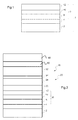
- Fig. 1 illustrates a back contact substrate 1 for a photovoltaic cell comprising:
- a formed (or deposited) on B is understood to mean A is formed either directly on B and thus in contact with B or formed on B with interposition of one or more thin films between A and B.
- electrode is understood to mean an electrical current transport coating comprising at least one thin film which conducts electrons, that is to say having a conductivity which is provided by the mobility of electrons.
- a material based on A that the material is mainly made of A, so that its aimed function is fulfilled. It preferably contains at least 80% atomic percent of A, for example at least 90% atomic percent of A. If the material is "based on A and B", it is meant that it preferably contains at least 80% total atomic percent of A and B, for example at least 90% total atomic percent of A and B.
- total atomic content that the atomic contents of the elements are added. If the atomic content of A is 35% and the atomic content of B is 55%, the total atomic content of A and B is 90%.
- the barrier to alkali thin film 4 is, for example, based on one of: silicon nitride, silicon oxide, silicon oxynitride, silicon oxycarbide, aluminum oxide or aluminum oxynitride, as will be further explained below.
- the electrode 6 illustrated is composed:
- the metallic thin film 8 forms a main conductive coating of the electrode. It is essential for achieving the required conductance of the electrode 6 and will be further explained in detail below.
- the main conductive coating may comprise only the metallic thin film or several thin films including the metallic thin film.
- the metallic thin film is based on aluminum, and the metallic thin film 8 has a thickness of at most 300nm, preferably at most 100 nm, preferably at most 90 nm, preferably at most 80 nm.
- the metallic thin film 8 is based on aluminum.
- the barrier to selenization thin film 10 protects the metallic thin film 8 from selenization. It is, for example, a thin film of a metal nitride or oxynitride such as TiO x N y , MoO x N y , ZrO x N y , TaO x N y , AlO x N y or of a metal oxide such as MoO x or TiO x .
- a metal nitride or oxynitride such as TiO x N y , MoO x N y , ZrO x N y , TaO x N y , AlO x N y or of a metal oxide such as MoO x or TiO x .
- the barrier to selenization thin film has a thickness of at most 50 nm, preferably at most 30 nm, preferably at most 20 nm.
- the ohmic contact thin film 12 is for establishing a good electrical contact with the light absorbing chalogenide thin film to be deposited directly above. It is for example based on molybdenum or tungsten, before selenization.
- the barrier to selenization thin film 10 and the ohmic contact thin film 12 will be further explained below.
- Such a back contact substrate 1 is intended for the manufacture of a photoactive material with addition of sodium.
- This element is known to improve the performance of photoactive materials of CIS, CIGS or CIGSSe type.
- the sodium content is a key parameter in the process, the sodium migration from the glass towards the photoactive material needs to be controlled and so, the presence of an alkali barrier film 4 can be needed.
- the barrier to alkali thin film 4 can be omitted.
- alkali it is meant “alkali element” whatever its oxidation state, i.e. in metallic or ionic form.
- a typical glass substrate is for example, a soda-lime-silica glass and comprises sodium ions.
- Another technique for the manufacture of the photoactive material consists in using the migration of the sodium ions from the carrier substrate, for example made of glass, in order to form the photoactive material.
- the back contact substrate 1 does not have a barrier to alkali thin film 4 and the metallic thin film 8 is, for example, formed directly on the carrier substrate 2.
- the electrode 6 comprises one or more inserted thin films.
- the back contact substrate 1 comprises a carrier substrate 2 and an electrode 6 comprising:
- the metallic thin film 8 is for conducting the electrical current along the surface of the electrode 6, to the connectors.
- the mettalic thin film 8 has, for example, an atomic content of aluminum of at least 90%, for example of at least 95%.
- It is preferably pure. This is why it preferably contains one or more among the following additional elements: copper(Cu), nickel (Ni), platinum (Pt), molybdenum (Mo), beryllium (Be), ,manganese (Mn), magnesium (Mg), vanadium (V), Zinc (Zn), silicon (Si), with a total atomic content of at most 5%.
- These metals are for example additives for increasing the hardness or byproducts of the metallurgical processes (mining, refining, target manufacturing)
- the metallic thin film 8 contains oxygen (O) and/or nitrogen (N) with a total maximum atomic content of at most 5%, preferably at most 2%.
- the thickness of the metal film should be as low as possible. Using very thin films not only the materials cost can be reduced but also the throughput of the deposition equipment and hence cost of the manufacturing equipment itself.
- the sheet resistance of the back electrode should be sufficiently high in order to reduce ohmic losses that would limit the efficiency of the solar cell or module.
- the metallic thin film 8 has a thickness of at most 300nm, preferably at most 100 nm, preferably at most 90 nm, preferably at most 80 nm.
- its thickness is at least 40 nm, preferably at least 50 nm, preferably at least 60nm.
- the metallic thin film 8 has a resistivity of at most 15 ⁇ .cm, preferably of at most 10 ⁇ .cm, preferably at most 6 ⁇ Ohmcm.
- the metallic thin film 8 has preferably a sheet resistance below 2 ⁇ / ⁇ , preferably below 1 ⁇ / ⁇ .
- the barrier to selenization thin film 10 further protects the metallic thin film 8 from possible selenization and/or sulphurization. It should be noted that a thin film which protects from selenization also protects from sulphurization.
- barrier thin film to selenization is understood to mean a thin film of a material of any type capable of preventing or reducing the selenization of thin films covered with the barrier to selenization during the deposition, on the barrier to selenization, of thin films of semiconducting materials formed by selenization and/or sulphurization.
- the barrier to selenization within the meaning of the invention shows a proven effectiveness even at a thickness of 3 nm.
- a selenization possible test for determining if a material is suitable or not for a role as barrier to selenization is to compare a sample with and without a thin film of 5 nm of this material between the ohmic contact thin film 12 and the metallic thin film 8 and to subject the samples to a selenization, for example by heating at 520°C in a 100% selenium atmosphere at atmospheric pressure during 10 minutes. If the selenization of the metallic thin film 8 is reduced or prevented and the ohmic contact thin film 12 is entirely selenized, the material is effective.
- the material of the barrier to selenization thin film 10 is, for example, based on a metal nitride or oxynitride M'ON such as TiO x N y , MoO x N y , WO x N y , NbO x N y , ReO x N y ZrO x N y , TaO x N y , AlO x N y or of a metal oxide such as MoO x or TiO x .
- a metal nitride or oxynitride M'ON such as TiO x N y , MoO x N y , WO x N y , NbO x N y , ReO x N y ZrO x N y , TaO x N y , AlO x N y or of a metal oxide such as MoO x or TiO x .
- it is a material of any type suitable for protecting the metallic thin film 8 from a possible selenization or sulphurization.
- the material can also be based on a metal oxide, such as molybdenum oxide, titanium oxide or a mixed oxide of molybdenum and titanium.
- a metal oxide such as molybdenum oxide, titanium oxide or a mixed oxide of molybdenum and titanium.
- the oxynitrides are preferred to the oxides.
- it concerns a material based on at least one among Mo x O y N z , W x O y N z , Ta x O y N z , Nb x O y N z , Re x O y N z ,even more preferably Mo x O y N z .
- the barrier to selenization thin film has preferably a compressive stress between 0 and -10GPa, preferably between -1 and -5 GPa.
- the barrier to selenization thin film is also preferably nano-crystalline or amorphous with a grain size of at most 10nm.
- It may also be based on several metal oxynitrides MON, M'ON, etc. or several nitrides.
- nitrides, oxides and oxynitrides can be substoichiometric, stoichiometric or superstoichiometric respectively in nitrogen and oxygen.
- the barrier to selenization thin film has a molar composition O/(O+N) of at least 1 % and at most 50%.
- the barrier to selenization thin film has a molar composition M'/(M'+O+N) of at least 15% and at most 80%.
- the barrier to selenization 10 has a thickness of less than or equal to 100 nm, preferably of less than or equal to 60 nm, more preferably of less than or equal to 40 nm.
- the barrier to selenization 10 is very thin, there is a risk of it no longer having a significant effect. It thus has, for example, a thickness of at least 5 nm, preferably of at least 10 nm.
- the barrier to selenization 10 has a lower conductivity than the metallic thin film 8. For example, it has a resistivity of between 200 ⁇ ohm.cm and 1000 ⁇ ohm.cm, in the case of a thin film based on a metal oxide, nitride or oxynitride.
- the barrier to selenization 10 is, in addition, preferably capable of limiting the backward diffusion of the sodium ions towards the carrier substrate 2, that is to say the diffusion of the sodium ions from the top of the ohmic contact thin film 12 through the ohmic contact thin film 12 and towards the carrier substrate 2.
- the metal M used for the ohmic contact thin film 12 is capable of forming, after sulphurization and/or selenization, an ohmic contact thin film with a photoactive semiconducting material, in particular with a photoactive semiconducting material based on copper and selenium and/or sulphur chalcopyrite, for example a photoactive material of Cu(In,Ga)(S,Se) 2 type, in particular CIS or CIGS, CIGSSe, or also a material of Cu 2 (Zn,Sn)(S,Se) 4 type or a material of cadmium telluride (CdTe) or cadmium sulphide (CdS) types.
- a photoactive semiconducting material in particular with a photoactive semiconducting material based on copper and selenium and/or sulphur chalcopyrite, for example a photoactive material of Cu(In,Ga)(S,Se) 2 type, in particular CIS or CI
- an ohmic contact thin film is understood to mean a thin film of a material such that the current/voltage characteristic of the contact is nonrectifying and linear.
- the ohmic contact thin film 12 is the final ohmic contact thin film of the electrode 6, that is to say that the electrode 6 does not have another thin film above the thin film 12.
- the thin film 12 is intended to be fully transformed, by selenization and/or sulphurization, into Mo(S,Se) 2 , which material is not, on the other hand, regarded as a material "based on elemental molybedenum” but a material based on molybdenum disulphide, on molybdenum diselenide or on a mixture of molybdenum disulphide and diselenide.
- the substrate illustrated in Figure 1 and described above is an intermediate product in the manufacture of a photovoltaic cell or module. This intermediate product is subsequently transformed as a result of the process for the manufacture of the photoactive material.
- the back contact substrate 1 described above is understood as the intermediate product before transformation, which can be stored and dispatched to other production sites for the manufacture of the module.
- the ohmic contact thin film 12, so as to act as ohmic contact once transformed into Mo(S,Se) 2 for example has a thickness of at least 10 nm and at most 100 nm before selenization, preferably of at least 30 nm and at most 50 nm. A large thickness is not necessary. After selenization, Mo(S,Se) 2 has a thickness which is 3-4 times the thickness of the initial molybdenum thin film.
- the said metal M is advantageously molybdenum-based and/or tungsten-based.
- the molybdenum disulphide and/or diselenide compounds Mo(S,Se) 2 are materials having a proven effectiveness as ohmic contact thin film.
- Tungsten (W) is a material with similar chemical properties. It also forms chalcogenide semiconductors WS 2 and WSe 2 .
- Mo(S,Se) 2 and W(S,Se) 2 can both be formed as p type semiconductors. More generally still, it concerns a metal M of any type capable of forming, after sulphurization and/or selenization, an ohmic contact thin film with a photoactive semiconducting material, more particularly with a photoactive material based on copper and selenium and/or sulphur chalcopyrite.
- the carrier substrate 2 and the barrier to alkali 4 will now be described.
- the carrier substrate can be rigid or flexible and can be made of a variety of materials such as soda-lime-silica or borosilicate glass, ceramic sheets, metal films, or polymer films.
- Two cases may be distinguished: the case where alkali are added on the back contact substrate during or before the formation of the absorber thin film (first case) and the case where only migration of alkali from the carrier substrate is used for doping the absorber thin film (second case).
- the substrates provided with one or more barrier to alkali thin films 4 are used in the first case, in particular in order to make it possible to use, as substrate, a sheet of glass of soda-lime-silica type obtained by the float process, glass of relatively low cost which exhibits all the qualities which are known in this type of material, such as, for example, its transparency, its impermeability to water and its hardness.
- the content of alkali species of the substrate 2 is, in this case, a disadvantage which the barrier to alkali thin film 4 will minimize, since only alkali from the addition on the back contact substrate and in a controlled amount are wanted.
- the barrier to alkali 4 is preferably based on at least one of the materials chosen from: silicon nitride, silicon oxide, silicon oxynitride, silicon oxycarbide, a mix of silicon oxycarbide and silicon oxynitride, aluminum oxide or aluminum oxynitride.
- a soda-lime-silica glass substrate is used without a barrier to alkali thin film but the alkali mobility is reduced by a matrix adaptation to benefit of the so-called mixed-alkali effect.
- the sodium content that may diffuse through the electrode to dope the photoactive material is significantly reduced and alkali are added during or before formation of the absorber thin film.
- the carrier substrate 2 is a sheet of a material of any appropriate type not comprising alkali species, for example a silica-based glass not comprising alkali species such as borosilicate glasses, high-strain point glass or made of plastic, or even of metal.
- a silica-based glass not comprising alkali species such as borosilicate glasses, high-strain point glass or made of plastic, or even of metal.
- the carrier substrate 2 is of any appropriate type comprising alkali species, for example comprising sodium ions and potassium ions.
- the substrate is, for example, a soda-lime-silica glass.
- the barrier to alkali thin film is absent.
- the carrier substrate 2 is intended to act as back contact in the photovoltaic module once the electrode is formed on it and thus does not need to be transparent.
- the sheet constituting the carrier substrate 2 can be flat or rounded, and can exhibit dimensions of any type, in particular at least one dimension of greater than 1 meter.
- Another subject-matter of the invention is a process for the manufacture of the back contact substrate 1 described above.
- the process comprises the stages consisting in:
- the deposition of the various thin films is, for example, carried out by magnetron cathode sputtering but, in an alternative form, another process of any appropriate type is used, e.g. thermal evaporation, chemical vapor deposition or electrochemical deposition.
- Another subject-matter of the invention is a semiconductor device 20 ( Figure 6 ) which uses the back contact substrate 1 described above to form one or more photoactive thin films 22, 24 thereon.
- the first photoactive thin film 22 is typically a doped thin film of p type, for example based on copper Cu, indium In, and selenium Se and/or sulphur S chalcopyrite. It can be, for example, as explained above, CIS, CIGS, CIGSSe or CZTS.
- the second photoactive thin film 24 is doped, of n type and described as buffer. It is, for example, composed of CdS (cadmium sulphide) and is formed directly on the first photoactive thin film 22.
- the buffer thin film 24 is, for example, based on In x S y , Zn(O,S) or ZnMgO or is made of another material of any appropriate type.
- the cell does not comprise a buffer thin film and the first photoactive thin film 22 itself forms a p-n homojunction.
- the first photoactive thin film 22 is a thin film of p type or having a p-n homojunction obtained by addition of alkali metal elements.
- the deposition of the photoactive thin film comprises stages of selenization and/or sulphurization, as explained in more detail below.
- the deposition can be carried out by evaporation of the elements Cu, In, Ga and Se (or Cu, Sn, Zn, S).
- the ohmic contact thin film 12 based on the metal M is transformed into a thin film 12' based on M(S,Se) 2 . This transformation concerns, for example, the whole of the ohmic contact thin film 12.
- the semiconducting device 20 thus comprises:
- the electrode 6' comprises:
- Another subject-matter of the invention is a photovoltaic cell 30 comprising a semiconducting device 20 as described above.
- the cell comprises, for example, as illustrated in Figure 6 :
- the transparent electrode 32 comprises, in an alternative form, a thin film of zinc oxide doped with gallium or boron, or also an indium tin oxide (ITO) thin film.
- ITO indium tin oxide
- TCO transparent conducting material
- the transparent electrode 32 is the so-called front electrode.
- the back electrode 6 is the electrode placed after the absorber thin film on the path of incoming light and the front electrode the one placed before. This is why a carrier substrate 2 with a back electrode 6 deposited on it is called a back contact substrate.
- a metal grid (not represented) is subsequently optionally deposited on the transparent electrode 32, for example through a mask, for example by an electron beam. It is, for example, an Al (aluminum) grid, for example with a thickness of approximately 2 ⁇ m, on which is deposited a Ni (nickel) grid, for example with a thickness of approximately 50 nm, in order to protect the Al thin film.
- the cell 30 is subsequently protected from external attacks. It comprises, for example, to this end, a counter-substrate 40 covering the front electrode 32 and laminated to the coated substrate, i.e. to the front electrode 32, via a lamination foil 50 made of a thermoplastic polymer. It is, for example, a sheet of EVA, PU or PVB.
- Another subject-matter of the invention is a photovoltaic module comprising several photovoltaic cells formed on the same substrate 2, which cells are connected to one another in series and are obtained by subsequent patterning and coating of the thin films of the semiconducting device 20.
- This monolithic integration of up to 100 individual cells is the state of the art for large area commercial thin film modules. It also includes the making of one to more than 100 laser P1 scribing trenches through the ohmic contact thin film 12, the barrier to selenization thin film 10 and the metallic thin film 8.
- Another subject-matter of the invention is a process for the manufacture of the semiconducting device 20 and of the photovoltaic cell 30 above, which process comprises a stage of formation of a photoactive thin film by selenization and/or sulphurization.
- the photoactive thin film 22 is, for example, a CIGS or CIGSSe thin film formed in the following way.
- the precursors of the thin film are deposited on the electrode 6.
- a metal stack composed of an alternation of thin films of CuGa and In type is, for example, deposited on the electrode 6 by magnetron cathode sputtering at ambient temperature.
- a thin film of selenium is subsequently deposited at ambient temperature directly on the metal stack, for example by thermal evaporation.
- the metal stack has, for example, a multilayer structure of Cu/In/Ga/Cu/In/Ga... type.
- the substrate is subjected to a heating treatment at high temperature, referred to as RTP ("Rapid Thermal Process"), for example at approximately 520°C, in an atmosphere composed, for example, of gaseous sulphur, for example based on S or H 2 S, thus forming a thin film of CuIn x Ga 1-x X(S,Se) 2 .
- RTP Rapid Thermal Process
- One advantage of this process is that it does not require an external source of selenium vapour.
- the loss of a portion of the selenium during the heating is compensated for by an excess deposition of selenium on the metal stack.
- the selenium necessary for the selenization is provided by the deposited thin film of selenium.
- the selenization is obtained without the deposition of a thin film of selenium but by an atmosphere comprising gaseous selenium, for example based on Se or H 2 Se, prior to the exposure to an atmosphere rich in sulphur.
- the alkali species Prior to the deposition of the CuGa and In metal stack, the alkali species are, for example, introduced by the deposition, on the sacrificial molybdenum-based thin film 12, of a thin film of sodium selenide or of a compound comprising sodium, so as to introduce, for example, of the order of 2 ⁇ 10 15 sodium atoms per cm 2 .
- the metal stack is deposited directly on this thin film of sodium selenide.
- CZTS may also be formed with a similar process.
- the process for the manufacture of the photoactive thin film 22 is of any appropriate type.
- An important aspect of the invention is that the electrode has reached its final properties after deposition and is compatible with low temperature processes and high temperature processes.
- the picture on the left corresponds a stack of glass/ Si 3 N 4 (140nm)/ Mo(200nm)/ TiON(15nm)/ Mo(30nm) stack
- the one in the centre corresponds to a glass/ Si 3 N 4 (140nm)/ Cu(100nm)/ MoON(15nm)/ Mo(30nm)
- the picture on the right is a glass/ Si 3 N 4 (140nm)/ Mo(400nm) stack.
- the molybdenum thin film can be sufficiently protected with thin films of TiON. Further analysis (not shown here) confirms that thin films of MoN also sufficiently protect molybdenum base thin films.
- the unprotected Mo thin film (right) was fully selenized and delaminated from the glass/ Si 3 N 4 substrate.
- the thin film stack of glass/ Si 3 N 4 (140nm)/ Cu(100nm)/ MoN(15nm)/ Mo30nm (centre) has been non-uniformly selenized, particularly in the P1 patterning lines and in many small spots in the cell area.
- the selenization test showed that Al could be sufficiently protected by a thin TiON thin film ( FIG. 4 ): in this test, which shows mass gain after selenization for three different stacks, and thus resistance to selenization, the weight gain of the protected Al/TiON/Mo thin films is a factor of 4 lower than the unprotected Mo thin films ( Figure 4a ).
- the reference of Molybdenum (on the right) did not peel off.
- the aluminum thin films did not delaminate, -see photo in Fig. 4b , which shows a photograph after selenization test of glass/Si3N4(90nm)/ Al(65nm)/ TiON(13nm)/ Mo(35nm)-.
- the degree of selenization can therefore be directly expressed by the weight difference before and after selenization.
- the weight gain is due to the selenium bound in the MoSe 2 thin film.
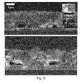
- Fig.5 shows SEM cross sections of CIGSSe absorbers
- Thickness of the Aluminum thin film is the thickness of the Aluminum thin film
- Table I shows examples of aluminum thin films and complete back electrodes stacks comprising the alkali barrier, the aluminum thin film, the barrier to selenization thin film and the Mo top thin film.
- resitivity values below 5 ⁇ Ohmcm can be obtained for example by magnetron sputtering.
- thickness values as low as 65nm are sufficient.
- a back electrode using only a single molybenum thin film a thickness of at least 200nm is required. Considering the much lower market price of aluminum metal and the low value of required thickness the cost of the back electrode is strongly reduced.
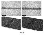
- FIG. 6 shows microscope images of P1 patterning lines with Al thicknesses of 130nm (a) and 65nm (b).
- Top row light microscopy images
- bottom row confocal microscope height profile maps.
- the thicker thin film showed a large rim or lift-off on both edges of the P1 trench. Such a rim could lead to a disturbed growth of the subsequent thin films or could lead to shunting within the solar cell.
- the lift-off should be significantly smaller than the thickness of the absorber thin film (1-2 ⁇ m) in order to ensure a continuous coating.
- Fig.7 shows lift-off height at the edges of P1 trenches in glass/ Si 3 N 4 / Al/ TiON/ Mo stacks determined by confocal microscopy as a function of the aluminum layer thickness.
- the lift-off strongly decreased with aluminum thin film thickness. The decrease is not trivial as in some cases a reduction of the thickness by a factor of 2 leads to a reduction of lift-off height by a factor of 4.
Landscapes
- Engineering & Computer Science (AREA)
- Microelectronics & Electronic Packaging (AREA)
- Computer Hardware Design (AREA)
- Power Engineering (AREA)
- Physics & Mathematics (AREA)
- Condensed Matter Physics & Semiconductors (AREA)
- Electromagnetism (AREA)
- General Physics & Mathematics (AREA)
- Chemical & Material Sciences (AREA)
- Life Sciences & Earth Sciences (AREA)
- Sustainable Energy (AREA)
- Crystallography & Structural Chemistry (AREA)
- Sustainable Development (AREA)
- Inorganic Chemistry (AREA)
- Photovoltaic Devices (AREA)
Priority Applications (3)
| Application Number | Priority Date | Filing Date | Title |
|---|---|---|---|
| EP20130191972 EP2871681A1 (de) | 2013-11-07 | 2013-11-07 | Rückseitenkontaktsubstrat für eine Solarzelle oder Modul |
| CN201480060971.3A CN105706244A (zh) | 2013-11-07 | 2014-11-07 | 用于光伏电池或模块的背接触基板 |
| PCT/EP2014/074011 WO2015067738A1 (en) | 2013-11-07 | 2014-11-07 | Back contact substrate for a photovoltaic cell or module |
Applications Claiming Priority (1)
| Application Number | Priority Date | Filing Date | Title |
|---|---|---|---|
| EP20130191972 EP2871681A1 (de) | 2013-11-07 | 2013-11-07 | Rückseitenkontaktsubstrat für eine Solarzelle oder Modul |
Publications (1)
| Publication Number | Publication Date |
|---|---|
| EP2871681A1 true EP2871681A1 (de) | 2015-05-13 |
Family
ID=49518872
Family Applications (1)
| Application Number | Title | Priority Date | Filing Date |
|---|---|---|---|
| EP20130191972 Withdrawn EP2871681A1 (de) | 2013-11-07 | 2013-11-07 | Rückseitenkontaktsubstrat für eine Solarzelle oder Modul |
Country Status (3)
| Country | Link |
|---|---|
| EP (1) | EP2871681A1 (de) |
| CN (1) | CN105706244A (de) |
| WO (1) | WO2015067738A1 (de) |
Cited By (3)
| Publication number | Priority date | Publication date | Assignee | Title |
|---|---|---|---|---|
| KR20180043113A (ko) * | 2016-10-19 | 2018-04-27 | 한국과학기술연구원 | 박막 태양전지 모듈 구조 및 이의 제조 방법 |
| WO2018139945A1 (en) * | 2017-01-25 | 2018-08-02 | Saule Sp. Z O.O. | Optoelectronic foil and manufacturing method of optoelectronic foil |
| EP4064378A1 (de) | 2021-03-23 | 2022-09-28 | Saule S.A. | Lichtdurchlässige mehrschichtstruktur für optoelektronische vorrichtungen |
Families Citing this family (1)
| Publication number | Priority date | Publication date | Assignee | Title |
|---|---|---|---|---|
| CN107742650A (zh) * | 2017-08-31 | 2018-02-27 | 成都中建材光电材料有限公司 | 一种具有绒面背接触层的碲化镉太阳能电池及其制备方法 |
Citations (6)
| Publication number | Priority date | Publication date | Assignee | Title |
|---|---|---|---|---|
| US5626688A (en) | 1994-12-01 | 1997-05-06 | Siemens Aktiengesellschaft | Solar cell with chalcopyrite absorber layer |
| WO2002065554A1 (fr) | 2001-01-31 | 2002-08-22 | Saint-Gobain Glass France | Sustrat transparent muni d'une electrode |
| WO2009080931A1 (fr) | 2007-12-07 | 2009-07-02 | Saint-Gobain Glass France | Perfectionnements apportes a des elements capables de collecter de la lumiere |
| US20120132281A1 (en) * | 2010-11-26 | 2012-05-31 | Nexpower Technology Corporation | Thin-film solar cell and manufacturing method thereof |
| US20120167979A1 (en) * | 2010-12-30 | 2012-07-05 | National Cheng Kung University | Thin film solar cell and method for manufacturing the same |
| FR2982422A1 (fr) * | 2011-11-09 | 2013-05-10 | Saint Gobain | Substrat conducteur pour cellule photovoltaique |
-
2013
- 2013-11-07 EP EP20130191972 patent/EP2871681A1/de not_active Withdrawn
-
2014
- 2014-11-07 CN CN201480060971.3A patent/CN105706244A/zh active Pending
- 2014-11-07 WO PCT/EP2014/074011 patent/WO2015067738A1/en active Application Filing
Patent Citations (8)
| Publication number | Priority date | Publication date | Assignee | Title |
|---|---|---|---|---|
| US5626688A (en) | 1994-12-01 | 1997-05-06 | Siemens Aktiengesellschaft | Solar cell with chalcopyrite absorber layer |
| WO2002065554A1 (fr) | 2001-01-31 | 2002-08-22 | Saint-Gobain Glass France | Sustrat transparent muni d'une electrode |
| US20120167961A1 (en) * | 2001-01-31 | 2012-07-05 | Saint-Gobain Glass France | Transparent substrate equipped with an electrode |
| WO2009080931A1 (fr) | 2007-12-07 | 2009-07-02 | Saint-Gobain Glass France | Perfectionnements apportes a des elements capables de collecter de la lumiere |
| US20100300512A1 (en) * | 2007-12-07 | 2010-12-02 | Saint-Gobain Glass France | Made to elements capable of collecting light |
| US20120132281A1 (en) * | 2010-11-26 | 2012-05-31 | Nexpower Technology Corporation | Thin-film solar cell and manufacturing method thereof |
| US20120167979A1 (en) * | 2010-12-30 | 2012-07-05 | National Cheng Kung University | Thin film solar cell and method for manufacturing the same |
| FR2982422A1 (fr) * | 2011-11-09 | 2013-05-10 | Saint Gobain | Substrat conducteur pour cellule photovoltaique |
Cited By (4)
| Publication number | Priority date | Publication date | Assignee | Title |
|---|---|---|---|---|
| KR20180043113A (ko) * | 2016-10-19 | 2018-04-27 | 한국과학기술연구원 | 박막 태양전지 모듈 구조 및 이의 제조 방법 |
| WO2018139945A1 (en) * | 2017-01-25 | 2018-08-02 | Saule Sp. Z O.O. | Optoelectronic foil and manufacturing method of optoelectronic foil |
| EP4064378A1 (de) | 2021-03-23 | 2022-09-28 | Saule S.A. | Lichtdurchlässige mehrschichtstruktur für optoelektronische vorrichtungen |
| WO2022200357A1 (en) | 2021-03-23 | 2022-09-29 | Saule S.A. | A light-transmissive multilayer structure for optoelectronic devices |
Also Published As
| Publication number | Publication date |
|---|---|
| CN105706244A (zh) | 2016-06-22 |
| WO2015067738A1 (en) | 2015-05-14 |
Similar Documents
| Publication | Publication Date | Title |
|---|---|---|
| Platzer-Björkman et al. | Back and front contacts in kesterite solar cells: state-of-the-art and open questions | |
| Kessler et al. | Technological aspects of flexible CIGS solar cells and modules | |
| US20140338741A1 (en) | Conducting substrate for a photovoltaic cell | |
| EP2800146A1 (de) | Rückseitenkontaktiertes Substrat für eine Photovoltaikzelle oder ein Photovoltaikmodul | |
| US20160056312A1 (en) | Back contact substrate for a photovoltaic cell or module | |
| CN101326645A (zh) | 太阳能电池 | |
| EP2800145B1 (de) | Rückseitenkontaktiertes Substrat für eine Photovoltaikzelle oder ein Photovoltaikmodul | |
| KR20140148407A (ko) | 광전 박막 태양 전지용 다층 후면 전극, 박막 태양 전지 및 모듈을 제조하기 위한 다층 후면 전극의 사용, 다층 후면 전극을 포함한 광전 박막 태양 전지 및 모듈, 및 그 제조 방법 | |
| AU2017200544A1 (en) | Multi-layer back electrode for a photovoltaic thin-film solar cell and use of the same for producing thin-film solar cells and modules, photovoltaic thin-film solar cells and modules containing the multi-layer back electrode, and method for the production thereof | |
| US7777127B2 (en) | Flexible solar cell | |
| EP2871681A1 (de) | Rückseitenkontaktsubstrat für eine Solarzelle oder Modul | |
| CN105742390A (zh) | 一种叠层薄膜太阳能电池及其制备方法 | |
| EP2999006A1 (de) | Vorrichtung zur photoelektrischen umwandlung, solarzelle und verfahren zur herstellung der vorrichtung zur photoelektrischen umwandlung | |
| JP6147926B2 (ja) | ナトリウムインジウム硫化物緩衝層を有する薄膜太陽電池のための層システム | |
| JP2011119478A (ja) | 化合物半導体太陽電池 | |
| KR102227799B1 (ko) | Cigs 박막 태양전지 제조방법 | |
| US9214575B2 (en) | Solar cell contact and method of making the contact | |
| US20140352786A1 (en) | ZnO-BASED SPUTTERING TARGET AND PHOTOVOLTAIC CELL HAVING PASSIVATION LAYER DEPOSITED USING THE SAME | |
| US20140261689A1 (en) | Method of manufacturing a photovoltaic device | |
| EP2940737A1 (de) | Herstellungsverfahren für zusammengesetzte dünnschichtsolarzelle |
Legal Events
| Date | Code | Title | Description |
|---|---|---|---|
| PUAI | Public reference made under article 153(3) epc to a published international application that has entered the european phase |
Free format text: ORIGINAL CODE: 0009012 |
|
| 17P | Request for examination filed |
Effective date: 20131107 |
|
| AK | Designated contracting states |
Kind code of ref document: A1 Designated state(s): AL AT BE BG CH CY CZ DE DK EE ES FI FR GB GR HR HU IE IS IT LI LT LU LV MC MK MT NL NO PL PT RO RS SE SI SK SM TR |
|
| AX | Request for extension of the european patent |
Extension state: BA ME |
|
| R17P | Request for examination filed (corrected) |
Effective date: 20151113 |
|
| RBV | Designated contracting states (corrected) |
Designated state(s): AL AT BE BG CH CY CZ DE DK EE ES FI FR GB GR HR HU IE IS IT LI LT LU LV MC MK MT NL NO PL PT RO RS SE SI SK SM TR |
|
| 17Q | First examination report despatched |
Effective date: 20171205 |
|
| STAA | Information on the status of an ep patent application or granted ep patent |
Free format text: STATUS: THE APPLICATION IS DEEMED TO BE WITHDRAWN |
|
| 18D | Application deemed to be withdrawn |
Effective date: 20190514 |