EP2869668A1 - Light emitting diode driving apparatus - Google Patents
Light emitting diode driving apparatus Download PDFInfo
- Publication number
- EP2869668A1 EP2869668A1 EP20140275096 EP14275096A EP2869668A1 EP 2869668 A1 EP2869668 A1 EP 2869668A1 EP 20140275096 EP20140275096 EP 20140275096 EP 14275096 A EP14275096 A EP 14275096A EP 2869668 A1 EP2869668 A1 EP 2869668A1
- Authority
- EP
- European Patent Office
- Prior art keywords
- light emitting
- emitting diode
- hysteresis
- control switch
- driving
- Prior art date
- Legal status (The legal status is an assumption and is not a legal conclusion. Google has not performed a legal analysis and makes no representation as to the accuracy of the status listed.)
- Granted
Links
- 238000001514 detection method Methods 0.000 claims description 8
- 230000005669 field effect Effects 0.000 description 5
- 101710170230 Antimicrobial peptide 1 Proteins 0.000 description 4
- 230000008901 benefit Effects 0.000 description 4
- 239000004065 semiconductor Substances 0.000 description 2
- 239000003990 capacitor Substances 0.000 description 1
- 238000009499 grossing Methods 0.000 description 1
- 238000012986 modification Methods 0.000 description 1
- 230000004048 modification Effects 0.000 description 1
- 238000004806 packaging method and process Methods 0.000 description 1
- 230000006798 recombination Effects 0.000 description 1
- 238000005215 recombination Methods 0.000 description 1
Images
Classifications
-
- H—ELECTRICITY
- H05—ELECTRIC TECHNIQUES NOT OTHERWISE PROVIDED FOR
- H05B—ELECTRIC HEATING; ELECTRIC LIGHT SOURCES NOT OTHERWISE PROVIDED FOR; CIRCUIT ARRANGEMENTS FOR ELECTRIC LIGHT SOURCES, IN GENERAL
- H05B45/00—Circuit arrangements for operating light-emitting diodes [LED]
-
- H—ELECTRICITY
- H05—ELECTRIC TECHNIQUES NOT OTHERWISE PROVIDED FOR
- H05B—ELECTRIC HEATING; ELECTRIC LIGHT SOURCES NOT OTHERWISE PROVIDED FOR; CIRCUIT ARRANGEMENTS FOR ELECTRIC LIGHT SOURCES, IN GENERAL
- H05B45/00—Circuit arrangements for operating light-emitting diodes [LED]
- H05B45/40—Details of LED load circuits
- H05B45/44—Details of LED load circuits with an active control inside an LED matrix
- H05B45/46—Details of LED load circuits with an active control inside an LED matrix having LEDs disposed in parallel lines
-
- H—ELECTRICITY
- H05—ELECTRIC TECHNIQUES NOT OTHERWISE PROVIDED FOR
- H05B—ELECTRIC HEATING; ELECTRIC LIGHT SOURCES NOT OTHERWISE PROVIDED FOR; CIRCUIT ARRANGEMENTS FOR ELECTRIC LIGHT SOURCES, IN GENERAL
- H05B45/00—Circuit arrangements for operating light-emitting diodes [LED]
- H05B45/30—Driver circuits
- H05B45/37—Converter circuits
-
- H—ELECTRICITY
- H05—ELECTRIC TECHNIQUES NOT OTHERWISE PROVIDED FOR
- H05B—ELECTRIC HEATING; ELECTRIC LIGHT SOURCES NOT OTHERWISE PROVIDED FOR; CIRCUIT ARRANGEMENTS FOR ELECTRIC LIGHT SOURCES, IN GENERAL
- H05B45/00—Circuit arrangements for operating light-emitting diodes [LED]
- H05B45/40—Details of LED load circuits
- H05B45/44—Details of LED load circuits with an active control inside an LED matrix
- H05B45/48—Details of LED load circuits with an active control inside an LED matrix having LEDs organised in strings and incorporating parallel shunting devices
Definitions
- an AC direct driving type LED driving circuit in which an LED is directly driven with AC power, a smoothing capacitor is not used, such that the LED driving circuit has advantages in terms of a lifespan, a size, and the like.
- An aspect of the present disclosure may provide an alternating current (AC) direct driving type light emitting diode (LED) driving apparatus capable of preventing a flicker phenomenon that may occur at a boundary at which the number of LED groups that are turned on is changed.
- AC alternating current
- LED light emitting diode
- the controlling unit may include a plurality of controllers limiting the operations of the respective drivers based on drain voltages of the respective control switches and the hysteresis reference value.
- the controlling unit may turn on the control switch in the case in which the level of the drain voltage of the control switch is higher than the hysteresis reference value and turn off the control switch in the case in which the drain voltage of the control switch has a level lower than that of the hysteresis reference value.
- the plurality of hysteresis switches may be FETs, and drains of the plurality of hysteresis switches may be connected to the outputs of the plurality of driving comparators, respectively.
- the light emitting diode driving apparatus may further include a rectifying unit rectifying AC power and supplying the rectified power to the light emitting diode.
- the first control switch M1 may be connected to a cathode of the first light emitting diode LED1.
- the first control switch M1 may be a field effect transistor (FET).
- the first control switch M1 may be turned off.
- any one of second to N-th control switches M2 to Mn may be turned on based on an increase amount in the detection voltage.
- the controlling unit 400 may include a plurality of controllers 400-1 to 400-N.
- controlling unit 400 may include a second controller 400-2 corresponding to the second driver 300-2, a third controller 400-3 corresponding to the third driver 300-3, and an N-th controller 400-N corresponding to the N-th driver 300-N.
- the limiting comparator 420 may have hysteresis characteristics. Since the limiting comparator 420 has the hysteresis characteristics, in the case in which the limitation of the driving by the controlling unit 400 is released, reoccurrence of the flicker phenomenon may be prevented.
- FIG. 3 is a view showing a light emitting diode driving apparatus according to another exemplary embodiment of the present disclosure.
- the first hysteresis switch 440-1 may be a field effect transistor, and may be connected between the light emitting diode LED1 and the first control switch M1.
- the flicker phenomenon that may occur when the number of LED groups that are turned on is changed in the AC direct driving type light emitting diode driving apparatus may be prevented.
Landscapes
- Circuit Arrangement For Electric Light Sources In General (AREA)
Abstract
Description
- This application claims the benefit of Korean Patent Application No.
10-2013-0131561 filed on October 31, 2013 - The present disclosure relates to a light emitting diode (LED) driving apparatus capable of driving a light emitting diode directly, using alternating current (AC) power.
- Light emitting diodes (LEDs), a semiconductor devices having a p-n junction structure and emitting light through the recombination of electrons and holes, has recently been applied to various technological fields in accordance with the development of semiconductor technology. Particularly, since LEDs have higher degrees of efficiency, longer effective lifespans and are more environment-friendly than existing light emitting devices, fields to which LEDs are applied have continuously increased.
- Generally, LEDs are driven by direct current (DC) power having a level of several volts applied thereto in view of a structure thereof. Therefore, generally, in order to drive LEDs with commercially available alternating current (AC) power used domestically, commercially or industrially, a separate unit is required. In order to drive an LED with commercial AC power, an LED driving apparatus generally includes a rectifying circuit, an AC to DC converter, and the like.
- However, since a general AC to DC converter has a relatively large volume and consumes a significant amount of power, when such a general AC to DC converter is used, advantages of LEDs such as high efficiency, a small packaging size, a long lifespan, and the like, are offset.
- Therefore, a large amount of research into apparatuses capable of driving LEDs directly with AC power, without the need for an AC to DC converter, has recently been undertaken.
- In an AC direct driving type LED driving circuit in which an LED is directly driven with AC power, a smoothing capacitor is not used, such that the LED driving circuit has advantages in terms of a lifespan, a size, and the like.
- In the case of driving an LED directly with AC power, without the use of an AC to DC converter, a plurality of switches are connected to a plurality of LEDs, respectively, and corresponding LED groups are driven while being turned on or off based on a level of the AC power. That is, an AC direct driving type LED driving circuit may control the LED groups to be automatically turned on or off based on a change in an AC power voltage.
- Meanwhile, in the AC direct driving type LED driving apparatus, a flicker phenomenon may occur due to noise in an AC power voltage at a boundary at which the number of LED groups that are turned on is changed.
-
Patent Documents 1 to 6, listed below, do not disclose a configuration for preventing a flicker phenomenon due to noise in an AC power voltage at a boundary at which the number of LED groups that are turned on is changed. -
- (Patent Document 1) Korean Patent No.
10-0997050 - (Patent Document 2) Korean Patent Laid-Open Publication No.
2013-0017553 - An aspect of the present disclosure may provide an alternating current (AC) direct driving type light emitting diode (LED) driving apparatus capable of preventing a flicker phenomenon that may occur at a boundary at which the number of LED groups that are turned on is changed.
- According to an aspect of the present disclosure, a light emitting diode driving apparatus may include: a light emitting diode emitting light by receiving rectified power; a driver driving the light emitting diode based on a voltage level of the rectified power; and a controller limiting an operation of the driver based on a voltage applied to the driver and a hysteresis reference value.
- The driver may include: a driving comparator comparing a detection voltage based on a current flowing in the light emitting diode with a light emitting reference voltage; and a control switch switched based on a comparison result of the driving comparator to control the light emitting diode.
- The control switch may be connected to a cathode of the light emitting diode.
- The control switch may be a field effect transistor (FET).
- The controller may limit the operation of the driver based on a drain voltage of the control switch and the hysteresis reference value.
- The controller may turn on the control switch in the case in which the level of the drain voltage of the control switch is higher than the hysteresis reference value and turn off the control switch in the case in which the drain voltage of the control switch has a level lower than that of the hysteresis reference value.
- The controller may include: a limiting comparator comparing the drain voltage of the control switch with the hysteresis reference value; and a hysteresis switch connecting an output of the driving comparator to a ground based on a comparison result of the limiting comparator.
- The hysteresis switch may be a FET, and a drain of the hysteresis switch may be connected to the output of the driving comparator.
- The controller may include: a limiting comparator comparing a cathode terminal voltage of the light emitting diode with the hysteresis reference value; and a hysteresis switch controlling a connection between the light emitting diode and the control switch based on a comparison result of the limiting comparator.
- The hysteresis switch may be connected between the light emitting diode and the control switch.
- The light emitting diode driving apparatus may further include a rectifying unit rectifying alternating current (AC) power and supplying the rectified power to the light emitting diode.
- According to another aspect of the present disclosure, a light emitting diode driving apparatus may include: a light emitting diode unit including a plurality of light emitting diodes connected to one another in series, each of the plurality light emitting diodes emitting light by receiving rectified power; a driving unit including a plurality of drivers driving the plurality of light emitting diodes, respectively, based on a voltage level of the rectified power; and a controlling unit limiting operations of the respective drivers based on voltages applied to the respective drivers and a hysteresis reference value.
- Each of the plurality of drivers may include: a driving comparator comparing a detection voltage based on a current flowing in the light emitting diode with a light emitting reference voltage; and a control switch switched based on a comparison result of the driving comparator to control the light emitting diode.
- The light emitting reference voltages of each of the plurality of drivers may be different from one another.
- The control switch of each of the plurality of drivers may be connected to a cathode of a corresponding light emitting diode.
- The control switch may be a FET.
- The controlling unit may include a plurality of controllers limiting the operations of the respective drivers based on drain voltages of the respective control switches and the hysteresis reference value.
- The controlling unit may turn on the control switch in the case in which the level of the drain voltage of the control switch is higher than the hysteresis reference value and turn off the control switch in the case in which the drain voltage of the control switch has a level lower than that of the hysteresis reference value.
- The controlling unit may include: a plurality of limiting comparators comparing the drain voltages of the control switches with the hysteresis reference value, respectively; and a plurality of hysteresis switches connecting outputs of the driving comparators to a ground based on comparison results of the plurality of limiting comparators, respectively.
- The plurality of hysteresis switches may be FETs, and drains of the plurality of hysteresis switches may be connected to the outputs of the plurality of driving comparators, respectively.
- The light emitting diode driving apparatus may further include a rectifying unit rectifying AC power and supplying the rectified power to the light emitting diode.
- The above and other aspects, features and other advantages of the present disclosure will be more clearly understood from the following detailed description taken in conjunction with the accompanying drawings, in which:
-
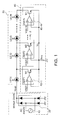
FIG. 1 is a view showing an alternating current (AC) direct driving type light emitting diode (LED) driving apparatus; -
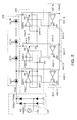
FIG. 2 is a view showing a light emitting diode driving apparatus according to an exemplary embodiment of the present disclosure; and -
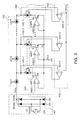
FIG. 3 is a view showing a light emitting diode driving apparatus according to another exemplary embodiment of the present disclosure. - Hereinafter, embodiments of the present disclosure will be described in detail with reference to the accompanying drawings. The disclosure may, however, be embodied in many different forms and should not be construed as being limited to the embodiments set forth herein. Rather, these embodiments are provided so that this disclosure will be thorough and complete, and will fully convey the scope of the disclosure to those skilled in the art. Throughout the drawings, the same or like reference numerals will be used to designate the same or like elements.
-
FIG. 1 is a view showing an alternating current (AC) direct driving type light emitting diode (LED) driving apparatus. - Referring to
FIG. 1 , the AC direct driving type light emitting diode driving apparatus may include apower supplying unit 10, a rectifyingunit 20, a lightemitting diode unit 30, and adriving unit 40. - The
power supplying unit 10 may supply AC power. - The rectifying
unit 20 may receive the AC power, full-wave or half-wave rectify the received AC power, and supply the rectified power to the lightemitting diode unit 30 to provide power capable of allowing the lightemitting diode unit 30 to emit light. - The light
emitting diode unit 30 may include a plurality of light emitting diodes LED1, LED2,···, LEDN connected to one another in series, and a corresponding light emitting diode may perform a light emitting operation by thedriving unit 40. - The
driving unit 40 may drive each of the plurality of light emitting diodes LED1, LED2,···, LEDN of the lightemitting diode unit 30. To this end, thedriving unit 40 may include a plurality of drivers 40-1, 40-2, ···, 40-N. - Each of the first to N-th drivers 40-1 to 40-N may be in charge of first to N-th light emitting diodes LED1 to LEDN of the light
emitting diode unit 30 to drive a corresponding light emitting diode. - In more detail, the first driver 40-1 may be in charge of driving of the first diode LED1. In addition, when a voltage level of the power rectified by the rectifying
unit 20 rises, an operation of the first driver 40-1 may be stopped, the second driver 40-2 may be in charge of driving of the first and second diodes LED1 and LED2, the third driver 40-3 to N-1-th driver 40-N-1 may be sequentially operated, and the N-th driver 40-N may be in charge of driving of the first to N-th light emitting diodes LED1 to LEDN. - Here, for example, in the case in which a voltage for driving the first and second diodes LED1 and LED2 is 90V, when the rectifying
unit 20 provides a voltage of 90V, a flicker phenomenon that the second diode LED2 flickers due to noise may occur. - For convenience of explanation, a minimum voltage value for driving the first diode LED1 will be defined as a first boundary voltage. Likewise, a minimum voltage value for driving the second diode LED2 will be defined as a second boundary voltage. In addition, a minimum voltage value for driving the N-th diode will be defined as an N-th boundary voltage.
- In the case in which the rectifying
unit 20 provides the first boundary voltage, a flicker phenomenon may occur in the first diode due to noise. Likewise, in the case in which the rectifyingunit 20 provides the second boundary voltage, a flicker phenomenon may occur in the second diode due to noise. - Therefore, each diode needs to be turned on at a voltage sufficiently larger than a boundary voltage in consideration of the noise.
-
FIG. 2 is a view showing a light emitting diode driving apparatus according to an exemplary embodiment of the present disclosure. - Referring to
FIG. 2 , the light emitting diode driving apparatus may include apower supplying unit 120, a rectifyingunit 140, a light emittingdiode unit 200, adriving unit 300, and a controllingunit 400. - The
power supplying unit 120 may supply AC power. - The rectifying
unit 140 may receive the AC power, full-wave or half-wave rectify the received AC power, and supply the rectified power to the light emittingdiode unit 200 to provide power capable of allowing light emitting diodes LED1 to LEDN to emit light. - The light emitting
diode unit 200 may include a plurality of light emitting diodes LED1, LED2,···, LEDN connected to each other in series, and a corresponding light emitting diode may perform a light emitting operation by the drivingunit 300. - The driving
unit 300 may drive each of the plurality of light emitting diodes LED1, LED2,···, LEDN of the light emittingdiode unit 200. To this end, the drivingunit 300 may include a plurality of drivers 300-1, 300-2, ···, 300-N. - Each of the first to N-th drivers 300-1, 300-2, ···, 300-N may be in charge of first to N-th light emitting diodes LED1 to LEDN of the light emitting
diode unit 200 to drive a corresponding light emitting diode. - In more detail, the first driver 300-1 may be in charge of driving of the first diode LED1. In addition, when a voltage level of the power rectified by the rectifying
unit 140 rises, an operation of the first driver 300-1 may be stopped, the second driver 300-2 may be in charge of driving of the first and second diodes LED1 and LED2, the third driver 300-3 to N-1-th driver 40-N-1 may be sequentially operated, and the N-th driver 300-N may be in charge of driving of the first to N-th light emitting diodes LED1 to LEDN. - That is, each of the first to N-th drivers 300-1, 300-2, ···, 300-N may drive the first to N-th light emitting diodes LED1 to LEDN corresponding thereto based on a voltage level of the rectified power. For example, in the case in which power rectified by the rectifying
unit 140 is the first boundary voltage or more, the first light emitting diode LED1 may be turned on. In addition, in the case in which power rectified by the rectifyingunit 140 is the second boundary voltage or more, the first and second light emitting diodes LED1 and LED2 may be turned on. - Referring to
FIG. 2 , the first driver 300-1 may include a first driving comparator AMP1 and a first control switch M1. - In detail, the first driving comparator AMP1 may compare a detection voltage based on a current flowing in the first light emitting diode LED1 with a light emitting reference voltage VREF1.
- The first control switch M1 may be connected to a cathode of the first light emitting diode LED1. In addition, the first control switch M1 may be a field effect transistor (FET).
- The first control switch M1 may be switched based on a comparison result of the first driving comparator to control the first light emitting diode LED1.
- In the case in which the detection voltage has a level lower than that of the light emitting reference voltage VREF1, the first control switch M1 may be maintained in a turn-on state.
- In the case in which the detection voltage is increased to thereby become larger than the light emitting reference voltage VREF1, the first control switch M1 may be turned off. In this case, any one of second to N-th control switches M2 to Mn may be turned on based on an increase amount in the detection voltage.
- Meanwhile, light emitting reference voltages VREF1 to VREFN of each of the plurality of drivers may be different from each other.
- The controlling
unit 400 may limit operations of the respective drivers 300-1 to 300-N based on voltages applied to the respective drivers 300-1 to 300-N and a hysteresis reference value Vthref. - The hysteresis reference value Vthref may mean a margin voltage for driving a light emitting diode while prevent flicker due to noise. That is, a predetermined light emitting diode may emit light only in the case in which a voltage of the hysteresis reference value or more is additionally applied thereto.
- The controlling
unit 400 may include a plurality of controllers 400-1 to 400-N. - In detail, the first controller 400-1 may limit an operation of the first driver 300-1 based on a voltage applied to the first driver 300-1 and the hysteresis reference value Vthref.
- In the case in which the first control switch M1 is implemented by the first field effect transistor, the voltage applied to the first driver 300-1 may be a drain voltage of the first control switch M1.
- The first controller 400-1 may turn on the first control switch M1 in the case in which the drain voltage of the first control switch M1 has a level higher than that of the hysteresis reference value Vthref. In addition, the first controller 400-1 may maintain the first control switch M1 in a turn-off state in the case in which the drain voltage of the first control switch M1 has a level lower than that of the hysteresis reference value Vthref.
- In detail, the first controller 400-1 may include a first limiting comparator 420-1 and a first hysteresis switch 440-1.
- Meanwhile, for convenience of explanation, a comparator used in the
driving unit 300 will be defined as a driving comparator, and a comparator used in the controllingunit 400 will be defined as a limiting comparator. - The first limiting comparator 420-1 may compare the drain voltage of the first control switch M1 with the hysteresis reference value Vthref.
- The first hysteresis switch 440-1 may connect an output of the first driving comparator AMP1 to a ground based on a comparison result of the first limiting comparator 420-1. In detail, the first hysteresis switch 440-1 may be a field effect transistor, and a drain thereof may be connected to the output of the first driving comparator AMP1.
- Therefore, the first limiting comparator 420-1 may turn on the first hysteresis switch 440-1 in the case in which the drain voltage of the first control switch M1 has a level lower than that of the hysteresis reference value Vthref. The hysteresis switch 440-1 is turned on, such that the driving of the first control switch M1 may be limited.
- The first limiting comparator 420-1 may turn off the first hysteresis switch 440-1 in the case in which the drain voltage of the first control switch M1 has a level higher than that of the hysteresis reference value Vthref. The hysteresis switch 440-1 is turned off, such that the limitation of the driving of the first control switch M1 may be released.
- Meanwhile, the controlling
unit 400 may include a second controller 400-2 corresponding to the second driver 300-2, a third controller 400-3 corresponding to the third driver 300-3, and an N-th controller 400-N corresponding to the N-th driver 300-N. - In this scheme, in the case in which a voltage applied to a drain of a predetermined control switch is sufficiently large, a corresponding light emitting diode is conducted, whereby the flicker phenomenon due to the noise may be prevented.
- For example, in the case in which the second boundary voltage is 90V, the second light emitting diode LED 2 may be turned on only when the voltage supplied by the rectifying
unit 140 is 90+Vthref V or more. - In addition, the limiting
comparator 420 according to an exemplary embodiment of the present disclosure may have hysteresis characteristics. Since the limitingcomparator 420 has the hysteresis characteristics, in the case in which the limitation of the driving by the controllingunit 400 is released, reoccurrence of the flicker phenomenon may be prevented. -
FIG. 3 is a view showing a light emitting diode driving apparatus according to another exemplary embodiment of the present disclosure. - Referring to
FIG. 3 , the light emitting diode driving apparatus according to another exemplary embodiment of the present disclosure is different in a configuration of a controllingunit 400 from the light emitting diode driving apparatus according to an exemplary embodiment of the present disclosure shown inFIG. 2 . Since configurations other than the controllingunit 400 are the same as those of the light emitting diode driving apparatus according to an exemplary embodiment of the present disclosure shown inFIG. 2 , a detailed description thereof will be omitted. - Referring to
FIG. 3 , a first controller may include a first limiting comparator 420-1 and a first hysteresis switch 440-1. - The first limiting comparator 420-1 may compare a cathode terminal voltage of a corresponding light emitting diode LED1 with the hysteresis reference value Vthref.
- The first hysteresis switch 440-1 may control a connection between the light emitting diode LED1 and the first control switch M1 based on a comparison result of the first limiting comparator 420-1.
- In detail, the first hysteresis switch 440-1 may be a field effect transistor, and may be connected between the light emitting diode LED1 and the first control switch M1.
- Therefore, the first limiting comparator 420-1 may turn off the first hysteresis switch 440-1 in the case in which the cathode terminal voltage of the light emitting diode LED1 has a level lower than that of the hysteresis reference value Vthref. The hysteresis switch 440-1 is turned off, such that the driving of the first control switch M1 may be limited.
- The first limiting comparator 420-1 may turn on the first hysteresis switch 440-1 in the case in which the cathode terminal voltage of the light emitting diode LED1 has a level higher than that of the hysteresis reference value Vthref. The hysteresis switch 440-1 is turned on, such that the limitation of the driving of the first control switch M1 may be released.
- Meanwhile, the controlling
unit 400 may include a second controller corresponding to the second driver 300-2, a third controller corresponding to the third driver 300-3, and an N-th controller corresponding to the N-th driver 300-N. - As set forth above, according to exemplary embodiments of the present disclosure, the flicker phenomenon that may occur when the number of LED groups that are turned on is changed in the AC direct driving type light emitting diode driving apparatus may be prevented.
- While exemplary embodiments have been shown and described above, it will be apparent to those skilled in the art that modifications and variations could be made without departing from the spirit and scope of the present disclosure as defined by the appended claims.
Claims (15)
- A light emitting diode driving apparatus comprising:a light emitting diode emitting light by receiving rectified power;a driver driving the light emitting diode based on a voltage level of the rectified power; anda controller limiting an operation of the driver based on a voltage applied to the driver and a hysteresis reference value.
- The light emitting diode driving apparatus of claim 1, wherein the driver includes:a driving comparator comparing a detection voltage based on a current flowing in the light emitting diode with a light emitting reference voltage; anda control switch switched based on a comparison result of the driving comparator to control the light emitting diode.
- The light emitting diode driving apparatus of claim 2, wherein the controller limits the operation of the driver based on a drain voltage of the control switch and the hysteresis reference value.
- The light emitting diode driving apparatus of claim 3, wherein the controller turns on the control switch in the case in which the level of the drain voltage of the control switch is higher than the hysteresis reference value and turns off the control switch in the case in which the drain voltage of the control switch has a level lower than that of the hysteresis reference value.
- The light emitting diode driving apparatus of claim 3, wherein the controller includes:a limiting comparator comparing the drain voltage of the control switch with the hysteresis reference value; anda hysteresis switch connecting an output of the driving comparator to a ground based on a comparison result of the limiting comparator.
- The light emitting diode driving apparatus of claim 5, wherein the hysteresis switch is a FET, and
a drain of the hysteresis switch is connected to the output of the driving comparator. - The light emitting diode driving apparatus of claim 3, wherein the controller includes:a limiting comparator comparing a cathode terminal voltage of the light emitting diode with the hysteresis reference value; anda hysteresis switch controlling a connection between the light emitting diode and the control switch based on a comparison result of the limiting comparator.
- The light emitting diode driving apparatus of claim 7, wherein the hysteresis switch is connected between the light emitting diode and the control switch.
- A light emitting diode driving apparatus comprising:a light emitting diode unit including a plurality of light emitting diodes connected to one another in series, each of the plurality light emitting diodes emitting light by receiving rectified power;a driving unit including a plurality of drivers driving the plurality of light emitting diodes, respectively, based on a voltage level of the rectified power; anda controlling unit limiting operations of the respective drivers based on voltages applied to the respective drivers and a hysteresis reference value.
- The light emitting diode driving apparatus of claim 9, wherein each of the plurality of drivers includes:a driving comparator comparing a detection voltage based on a current flowing in the light emitting diode with a light emitting reference voltage; anda control switch switched based on a comparison result of the driving comparator to control the light emitting diode.
- The light emitting diode driving apparatus of claim 10, wherein the light emitting reference voltages of each of the plurality of drivers are different from one another.
- The light emitting diode driving apparatus of claim 10, wherein the controlling unit includes a plurality of controllers limiting the operations of the respective drivers based on drain voltages of the respective control switches and the hysteresis reference value.
- The light emitting diode driving apparatus of claim 12, wherein the controlling unit turns on the control switch in the case in which the level of the drain voltage of the control switch is higher than the hysteresis reference value and turns off the control switch in the case in which the drain voltage of the control switch has a level lower than that of the hysteresis reference value.
- The light emitting diode driving apparatus of claim 12, wherein the controlling unit includes:a plurality of limiting comparators comparing the drain voltages of the control switches with the hysteresis reference value, respectively; anda plurality of hysteresis switches connecting outputs of the driving comparators to a ground based on comparison results of the plurality of limiting comparators, respectively.
- The light emitting diode driving apparatus of claim 14, wherein the plurality of hysteresis switches are FETs, and
drains of the plurality of hysteresis switches are connected to the outputs of the plurality of driving comparators, respectively.
Applications Claiming Priority (1)
| Application Number | Priority Date | Filing Date | Title |
|---|---|---|---|
| KR1020130131561A KR101588695B1 (en) | 2013-10-31 | 2013-10-31 | Light emitting diode driving apparatus |
Publications (2)
| Publication Number | Publication Date |
|---|---|
| EP2869668A1 true EP2869668A1 (en) | 2015-05-06 |
| EP2869668B1 EP2869668B1 (en) | 2016-09-21 |
Family
ID=50630719
Family Applications (1)
| Application Number | Title | Priority Date | Filing Date |
|---|---|---|---|
| EP14275096.7A Not-in-force EP2869668B1 (en) | 2013-10-31 | 2014-04-29 | Light emitting diode driving apparatus |
Country Status (4)
| Country | Link |
|---|---|
| US (1) | US9301353B2 (en) |
| EP (1) | EP2869668B1 (en) |
| KR (1) | KR101588695B1 (en) |
| CN (1) | CN104602391B (en) |
Families Citing this family (18)
| Publication number | Priority date | Publication date | Assignee | Title |
|---|---|---|---|---|
| KR102209034B1 (en) * | 2014-07-30 | 2021-01-28 | 엘지이노텍 주식회사 | Light emitting module |
| US9462648B2 (en) * | 2014-10-20 | 2016-10-04 | Huizhou Light Engine Limited | Method and arrangement for remotely driving light emitting diodes from a three-phase power source via a single phase cable system |
| CN105657927B (en) * | 2014-11-14 | 2018-04-24 | 凹凸电子(武汉)有限公司 | The control circuit of the electric energy of light source driving circuit and control light source |
| US9439255B2 (en) | 2014-11-14 | 2016-09-06 | 02Micro Inc | Circuits for driving light sources |
| KR102335311B1 (en) * | 2014-11-20 | 2021-12-09 | 주식회사 엘엑스세미콘 | Lighting apparatus |
| CN107690834B (en) * | 2015-05-28 | 2019-12-27 | 飞利浦照明控股有限公司 | High efficiency lighting circuit for LED assembly |
| CN105188214B (en) * | 2015-09-07 | 2017-06-30 | 电子科技大学 | A kind of piece-wise linear constant current LED drive circuit |
| CN105188216B (en) * | 2015-09-07 | 2017-06-30 | 电子科技大学 | A kind of piece-wise linear constant current LED drive circuit |
| FR3042377B1 (en) * | 2015-10-09 | 2019-11-08 | Easii Ic | OPTOELECTRONIC CIRCUIT WITH ELECTROLUMINESCENT DIODES |
| US9615421B1 (en) * | 2015-11-11 | 2017-04-04 | Alfasemi Inc. | LED control circuit |
| CA2951301C (en) | 2015-12-09 | 2019-03-05 | Abl Ip Holding Llc | Color mixing for solid state lighting using direct ac drives |
| US9854637B2 (en) | 2016-05-18 | 2017-12-26 | Abl Ip Holding Llc | Method for controlling a tunable white fixture using a single handle |
| KR20170133731A (en) * | 2016-05-26 | 2017-12-06 | 김정숙 | advertising panel representing variable color backgrounds |
| US9848472B1 (en) * | 2017-03-02 | 2017-12-19 | Alfasemi Inc. | LED device with energy compensation |
| CN108696110B (en) * | 2018-07-10 | 2024-02-27 | 魏德米勒电联接(上海)有限公司 | Low-power consumption hysteresis driving device and driving method |
| US10874006B1 (en) | 2019-03-08 | 2020-12-22 | Abl Ip Holding Llc | Lighting fixture controller for controlling color temperature and intensity |
| US10728979B1 (en) | 2019-09-30 | 2020-07-28 | Abl Ip Holding Llc | Lighting fixture configured to provide multiple lighting effects |
| KR20230144378A (en) * | 2022-04-07 | 2023-10-16 | 삼성전자주식회사 | Display apparatus and control method thereof |
Citations (7)
| Publication number | Priority date | Publication date | Assignee | Title |
|---|---|---|---|---|
| DE3836792A1 (en) * | 1987-10-30 | 1989-05-24 | Hitachi Ltd | ERROR DETECTION DEVICE FOR AN OPTOCOUPLER AND AN OPTOCOUPLER DEVICE WITH AN ERROR DETECTION FUNCTION |
| US20070001995A1 (en) * | 2005-06-29 | 2007-01-04 | Lg.Philips Lcd Co., Ltd. | Apparatus and method for driving backlight |
| KR100997050B1 (en) | 2010-05-06 | 2010-11-29 | 주식회사 티엘아이 | Led lighting system for improving linghting amount |
| US20130027107A1 (en) * | 2011-07-25 | 2013-01-31 | Renesas Electronics Corporation | Signal conversion circuit, isolator circuit including the same, and signal conversion method |
| KR20130017553A (en) | 2011-08-11 | 2013-02-20 | 주식회사 실리콘웍스 | Under voltage lock out circuit |
| EP2645819A1 (en) * | 2012-03-30 | 2013-10-02 | Samsung Electro-Mechanics Co., Ltd | Light emitting diode driving apparatus |
| EP2680417A1 (en) * | 2012-06-28 | 2014-01-01 | Samsung Electro-Mechanics Co., Ltd | Light emitting diode driving apparatus |
Family Cites Families (10)
| Publication number | Priority date | Publication date | Assignee | Title |
|---|---|---|---|---|
| TW591866B (en) * | 1999-09-23 | 2004-06-11 | Texas Instruments Inc | Frequency control of hysteretic switch-mode power supply |
| US7081722B1 (en) | 2005-02-04 | 2006-07-25 | Kimlong Huynh | Light emitting diode multiphase driver circuit and method |
| JP4657799B2 (en) | 2005-05-11 | 2011-03-23 | 株式会社リコー | Light emitting diode drive circuit |
| US8324840B2 (en) * | 2009-06-04 | 2012-12-04 | Point Somee Limited Liability Company | Apparatus, method and system for providing AC line power to lighting devices |
| US20130069546A1 (en) * | 2010-11-23 | 2013-03-21 | O2Micro, Inc. | Circuits and methods for driving light sources |
| DE202012013553U1 (en) * | 2011-01-28 | 2017-09-26 | Seoul Semiconductor Co., Ltd. | LED luminescence |
| KR20130078500A (en) * | 2011-12-30 | 2013-07-10 | 매그나칩 반도체 유한회사 | Led driver circuit and light apparatus having the same in |
| CN103249217B (en) * | 2012-02-03 | 2015-05-06 | 日亚化学工业株式会社 | Light-emitting diode driving apparatus |
| KR20130095117A (en) * | 2012-02-17 | 2013-08-27 | 서울반도체 주식회사 | A driving apparutus for led |
| KR101474082B1 (en) * | 2012-12-28 | 2014-12-17 | 삼성전기주식회사 | Light emitting diode driving apparatus |
-
2013
- 2013-10-31 KR KR1020130131561A patent/KR101588695B1/en active Active
-
2014
- 2014-04-25 US US14/262,390 patent/US9301353B2/en not_active Expired - Fee Related
- 2014-04-29 EP EP14275096.7A patent/EP2869668B1/en not_active Not-in-force
- 2014-10-31 CN CN201410601515.7A patent/CN104602391B/en active Active
Patent Citations (8)
| Publication number | Priority date | Publication date | Assignee | Title |
|---|---|---|---|---|
| DE3836792A1 (en) * | 1987-10-30 | 1989-05-24 | Hitachi Ltd | ERROR DETECTION DEVICE FOR AN OPTOCOUPLER AND AN OPTOCOUPLER DEVICE WITH AN ERROR DETECTION FUNCTION |
| US20070001995A1 (en) * | 2005-06-29 | 2007-01-04 | Lg.Philips Lcd Co., Ltd. | Apparatus and method for driving backlight |
| KR100997050B1 (en) | 2010-05-06 | 2010-11-29 | 주식회사 티엘아이 | Led lighting system for improving linghting amount |
| US20110273103A1 (en) * | 2010-05-06 | 2011-11-10 | Tli Inc. | Led lamp with adjustable illumination intensity based on ac voltage amplitude |
| US20130027107A1 (en) * | 2011-07-25 | 2013-01-31 | Renesas Electronics Corporation | Signal conversion circuit, isolator circuit including the same, and signal conversion method |
| KR20130017553A (en) | 2011-08-11 | 2013-02-20 | 주식회사 실리콘웍스 | Under voltage lock out circuit |
| EP2645819A1 (en) * | 2012-03-30 | 2013-10-02 | Samsung Electro-Mechanics Co., Ltd | Light emitting diode driving apparatus |
| EP2680417A1 (en) * | 2012-06-28 | 2014-01-01 | Samsung Electro-Mechanics Co., Ltd | Light emitting diode driving apparatus |
Also Published As
| Publication number | Publication date |
|---|---|
| US9301353B2 (en) | 2016-03-29 |
| US20150115819A1 (en) | 2015-04-30 |
| KR101588695B1 (en) | 2016-01-28 |
| EP2869668B1 (en) | 2016-09-21 |
| CN104602391A (en) | 2015-05-06 |
| KR20150050122A (en) | 2015-05-08 |
| CN104602391B (en) | 2017-09-26 |
Similar Documents
| Publication | Publication Date | Title |
|---|---|---|
| EP2869668B1 (en) | Light emitting diode driving apparatus | |
| US20140184078A1 (en) | Light emitting diode driving device | |
| US9173265B2 (en) | Light emitting diode driving apparatus and light emitting diode lighting apparatus | |
| US8981649B2 (en) | Light emitting diode driving apparatus | |
| US9755634B2 (en) | Low current start up including power switch | |
| JP2011035368A (en) | Light-emitting diode driver and driving method of the same | |
| CN104868703A (en) | High voltage converter without auxiliary winding | |
| KR102286767B1 (en) | Control circuit for led lighting apparatus | |
| US8841851B2 (en) | Light emitting diode driving apparatus | |
| US20140167640A1 (en) | Back-up Capacitor | |
| US10070492B2 (en) | Dimming device | |
| KR20150001033A (en) | Power supplying apparatus | |
| US8669709B2 (en) | Solid state lighting driver with THDi bypass circuit | |
| US8981658B2 (en) | Apparatus for driving light emitting diode | |
| KR101320244B1 (en) | Light emitting diodes driver | |
| KR101587540B1 (en) | Light emitting diode apparatus | |
| EP2887770A2 (en) | Light emitting diode driver and method of controlling the same | |
| US8525426B2 (en) | Lighting apparatus and controlling method thereof | |
| KR101349576B1 (en) | CIRCUITS FOR CONTROLLING OF A light emitting diode | |
| KR101618818B1 (en) | Light emitting element driving circuit and driving method therefor | |
| JP2015210974A (en) | Lighting device and lighting device | |
| KR20160149555A (en) | Apparatus and method for driving light emitting diode | |
| KR20150074567A (en) | Ac direct connection type led control device | |
| KR20130017588A (en) | Ac to dc converter for driving led lamp |
Legal Events
| Date | Code | Title | Description |
|---|---|---|---|
| PUAI | Public reference made under article 153(3) epc to a published international application that has entered the european phase |
Free format text: ORIGINAL CODE: 0009012 |
|
| 17P | Request for examination filed |
Effective date: 20140429 |
|
| AK | Designated contracting states |
Kind code of ref document: A1 Designated state(s): AL AT BE BG CH CY CZ DE DK EE ES FI FR GB GR HR HU IE IS IT LI LT LU LV MC MK MT NL NO PL PT RO RS SE SI SK SM TR |
|
| AX | Request for extension of the european patent |
Extension state: BA ME |
|
| GRAP | Despatch of communication of intention to grant a patent |
Free format text: ORIGINAL CODE: EPIDOSNIGR1 |
|
| RAP1 | Party data changed (applicant data changed or rights of an application transferred) |
Owner name: SAMSUNG ELECTRO-MECHANICS CO., LTD. |
|
| INTG | Intention to grant announced |
Effective date: 20160412 |
|
| GRAS | Grant fee paid |
Free format text: ORIGINAL CODE: EPIDOSNIGR3 |
|
| GRAA | (expected) grant |
Free format text: ORIGINAL CODE: 0009210 |
|
| AK | Designated contracting states |
Kind code of ref document: B1 Designated state(s): AL AT BE BG CH CY CZ DE DK EE ES FI FR GB GR HR HU IE IS IT LI LT LU LV MC MK MT NL NO PL PT RO RS SE SI SK SM TR |
|
| REG | Reference to a national code |
Ref country code: GB Ref legal event code: FG4D |
|
| REG | Reference to a national code |
Ref country code: CH Ref legal event code: EP |
|
| REG | Reference to a national code |
Ref country code: AT Ref legal event code: REF Ref document number: 831951 Country of ref document: AT Kind code of ref document: T Effective date: 20161015 |
|
| REG | Reference to a national code |
Ref country code: IE Ref legal event code: FG4D |
|
| REG | Reference to a national code |
Ref country code: DE Ref legal event code: R096 Ref document number: 602014003842 Country of ref document: DE |
|
| REG | Reference to a national code |
Ref country code: NL Ref legal event code: FP |
|
| REG | Reference to a national code |
Ref country code: LT Ref legal event code: MG4D |
|
| PG25 | Lapsed in a contracting state [announced via postgrant information from national office to epo] |
Ref country code: FI Free format text: LAPSE BECAUSE OF FAILURE TO SUBMIT A TRANSLATION OF THE DESCRIPTION OR TO PAY THE FEE WITHIN THE PRESCRIBED TIME-LIMIT Effective date: 20160921 Ref country code: LT Free format text: LAPSE BECAUSE OF FAILURE TO SUBMIT A TRANSLATION OF THE DESCRIPTION OR TO PAY THE FEE WITHIN THE PRESCRIBED TIME-LIMIT Effective date: 20160921 Ref country code: RS Free format text: LAPSE BECAUSE OF FAILURE TO SUBMIT A TRANSLATION OF THE DESCRIPTION OR TO PAY THE FEE WITHIN THE PRESCRIBED TIME-LIMIT Effective date: 20160921 Ref country code: NO Free format text: LAPSE BECAUSE OF FAILURE TO SUBMIT A TRANSLATION OF THE DESCRIPTION OR TO PAY THE FEE WITHIN THE PRESCRIBED TIME-LIMIT Effective date: 20161221 |
|
| REG | Reference to a national code |
Ref country code: AT Ref legal event code: MK05 Ref document number: 831951 Country of ref document: AT Kind code of ref document: T Effective date: 20160921 |
|
| PG25 | Lapsed in a contracting state [announced via postgrant information from national office to epo] |
Ref country code: LV Free format text: LAPSE BECAUSE OF FAILURE TO SUBMIT A TRANSLATION OF THE DESCRIPTION OR TO PAY THE FEE WITHIN THE PRESCRIBED TIME-LIMIT Effective date: 20160921 Ref country code: GR Free format text: LAPSE BECAUSE OF FAILURE TO SUBMIT A TRANSLATION OF THE DESCRIPTION OR TO PAY THE FEE WITHIN THE PRESCRIBED TIME-LIMIT Effective date: 20161222 Ref country code: SE Free format text: LAPSE BECAUSE OF FAILURE TO SUBMIT A TRANSLATION OF THE DESCRIPTION OR TO PAY THE FEE WITHIN THE PRESCRIBED TIME-LIMIT Effective date: 20160921 |
|
| REG | Reference to a national code |
Ref country code: DE Ref legal event code: R081 Ref document number: 602014003842 Country of ref document: DE Owner name: SOLUM (HEFEI) SEMICONDUCTOR CO., LTD., HEFEI C, CN Free format text: FORMER OWNER: SAMSUNG ELECTRO-MECHANICS CO., LTD., SUWON-SI, GYEONGGI-DO, KR Ref country code: DE Ref legal event code: R082 Ref document number: 602014003842 Country of ref document: DE Representative=s name: MITSCHERLICH, PATENT- UND RECHTSANWAELTE PARTM, DE Ref country code: DE Ref legal event code: R081 Ref document number: 602014003842 Country of ref document: DE Owner name: SOLUM CO., LTD., SUWON-SI, KR Free format text: FORMER OWNER: SAMSUNG ELECTRO-MECHANICS CO., LTD., SUWON-SI, GYEONGGI-DO, KR Ref country code: DE Ref legal event code: R081 Ref document number: 602014003842 Country of ref document: DE Owner name: SOLUM CO., LTD., YONGIN-SI, KR Free format text: FORMER OWNER: SAMSUNG ELECTRO-MECHANICS CO., LTD., SUWON-SI, GYEONGGI-DO, KR Ref country code: DE Ref legal event code: R082 Ref document number: 602014003842 Country of ref document: DE Representative=s name: PATENTANWAELTE HENKEL, BREUER & PARTNER MBB, DE Ref country code: DE Ref legal event code: R082 Ref document number: 602014003842 Country of ref document: DE Representative=s name: PATENTANWAELTE HENKEL, BREUER & PARTNER, DE |
|
| PG25 | Lapsed in a contracting state [announced via postgrant information from national office to epo] |
Ref country code: EE Free format text: LAPSE BECAUSE OF FAILURE TO SUBMIT A TRANSLATION OF THE DESCRIPTION OR TO PAY THE FEE WITHIN THE PRESCRIBED TIME-LIMIT Effective date: 20160921 Ref country code: RO Free format text: LAPSE BECAUSE OF FAILURE TO SUBMIT A TRANSLATION OF THE DESCRIPTION OR TO PAY THE FEE WITHIN THE PRESCRIBED TIME-LIMIT Effective date: 20160921 |
|
| PG25 | Lapsed in a contracting state [announced via postgrant information from national office to epo] |
Ref country code: PT Free format text: LAPSE BECAUSE OF FAILURE TO SUBMIT A TRANSLATION OF THE DESCRIPTION OR TO PAY THE FEE WITHIN THE PRESCRIBED TIME-LIMIT Effective date: 20170123 Ref country code: ES Free format text: LAPSE BECAUSE OF FAILURE TO SUBMIT A TRANSLATION OF THE DESCRIPTION OR TO PAY THE FEE WITHIN THE PRESCRIBED TIME-LIMIT Effective date: 20160921 Ref country code: PL Free format text: LAPSE BECAUSE OF FAILURE TO SUBMIT A TRANSLATION OF THE DESCRIPTION OR TO PAY THE FEE WITHIN THE PRESCRIBED TIME-LIMIT Effective date: 20160921 Ref country code: CZ Free format text: LAPSE BECAUSE OF FAILURE TO SUBMIT A TRANSLATION OF THE DESCRIPTION OR TO PAY THE FEE WITHIN THE PRESCRIBED TIME-LIMIT Effective date: 20160921 Ref country code: IS Free format text: LAPSE BECAUSE OF FAILURE TO SUBMIT A TRANSLATION OF THE DESCRIPTION OR TO PAY THE FEE WITHIN THE PRESCRIBED TIME-LIMIT Effective date: 20170121 Ref country code: BG Free format text: LAPSE BECAUSE OF FAILURE TO SUBMIT A TRANSLATION OF THE DESCRIPTION OR TO PAY THE FEE WITHIN THE PRESCRIBED TIME-LIMIT Effective date: 20161221 Ref country code: BE Free format text: LAPSE BECAUSE OF FAILURE TO SUBMIT A TRANSLATION OF THE DESCRIPTION OR TO PAY THE FEE WITHIN THE PRESCRIBED TIME-LIMIT Effective date: 20160921 Ref country code: SK Free format text: LAPSE BECAUSE OF FAILURE TO SUBMIT A TRANSLATION OF THE DESCRIPTION OR TO PAY THE FEE WITHIN THE PRESCRIBED TIME-LIMIT Effective date: 20160921 Ref country code: AT Free format text: LAPSE BECAUSE OF FAILURE TO SUBMIT A TRANSLATION OF THE DESCRIPTION OR TO PAY THE FEE WITHIN THE PRESCRIBED TIME-LIMIT Effective date: 20160921 Ref country code: SM Free format text: LAPSE BECAUSE OF FAILURE TO SUBMIT A TRANSLATION OF THE DESCRIPTION OR TO PAY THE FEE WITHIN THE PRESCRIBED TIME-LIMIT Effective date: 20160921 |
|
| REG | Reference to a national code |
Ref country code: NL Ref legal event code: PD Owner name: SOLUM CO., LTD; KR Free format text: DETAILS ASSIGNMENT: CHANGE OF OWNER(S), ASSIGNMENT; FORMER OWNER NAME: SAMSUNG ELECTRO-MECHANICS CO., LTD. Effective date: 20170410 |
|
| REG | Reference to a national code |
Ref country code: DE Ref legal event code: R097 Ref document number: 602014003842 Country of ref document: DE |
|
| PG25 | Lapsed in a contracting state [announced via postgrant information from national office to epo] |
Ref country code: IT Free format text: LAPSE BECAUSE OF FAILURE TO SUBMIT A TRANSLATION OF THE DESCRIPTION OR TO PAY THE FEE WITHIN THE PRESCRIBED TIME-LIMIT Effective date: 20160921 |
|
| PLBE | No opposition filed within time limit |
Free format text: ORIGINAL CODE: 0009261 |
|
| STAA | Information on the status of an ep patent application or granted ep patent |
Free format text: STATUS: NO OPPOSITION FILED WITHIN TIME LIMIT |
|
| PG25 | Lapsed in a contracting state [announced via postgrant information from national office to epo] |
Ref country code: DK Free format text: LAPSE BECAUSE OF FAILURE TO SUBMIT A TRANSLATION OF THE DESCRIPTION OR TO PAY THE FEE WITHIN THE PRESCRIBED TIME-LIMIT Effective date: 20160921 |
|
| 26N | No opposition filed |
Effective date: 20170622 |
|
| PG25 | Lapsed in a contracting state [announced via postgrant information from national office to epo] |
Ref country code: SI Free format text: LAPSE BECAUSE OF FAILURE TO SUBMIT A TRANSLATION OF THE DESCRIPTION OR TO PAY THE FEE WITHIN THE PRESCRIBED TIME-LIMIT Effective date: 20160921 |
|
| REG | Reference to a national code |
Ref country code: CH Ref legal event code: PL |
|
| REG | Reference to a national code |
Ref country code: IE Ref legal event code: MM4A |
|
| REG | Reference to a national code |
Ref country code: FR Ref legal event code: ST Effective date: 20171229 |
|
| PG25 | Lapsed in a contracting state [announced via postgrant information from national office to epo] |
Ref country code: FR Free format text: LAPSE BECAUSE OF NON-PAYMENT OF DUE FEES Effective date: 20170502 Ref country code: MC Free format text: LAPSE BECAUSE OF FAILURE TO SUBMIT A TRANSLATION OF THE DESCRIPTION OR TO PAY THE FEE WITHIN THE PRESCRIBED TIME-LIMIT Effective date: 20160921 |
|
| PG25 | Lapsed in a contracting state [announced via postgrant information from national office to epo] |
Ref country code: LU Free format text: LAPSE BECAUSE OF NON-PAYMENT OF DUE FEES Effective date: 20170429 Ref country code: CH Free format text: LAPSE BECAUSE OF NON-PAYMENT OF DUE FEES Effective date: 20170430 Ref country code: LI Free format text: LAPSE BECAUSE OF NON-PAYMENT OF DUE FEES Effective date: 20170430 |
|
| PG25 | Lapsed in a contracting state [announced via postgrant information from national office to epo] |
Ref country code: IE Free format text: LAPSE BECAUSE OF NON-PAYMENT OF DUE FEES Effective date: 20170429 |
|
| PG25 | Lapsed in a contracting state [announced via postgrant information from national office to epo] |
Ref country code: MT Free format text: LAPSE BECAUSE OF NON-PAYMENT OF DUE FEES Effective date: 20170429 |
|
| PG25 | Lapsed in a contracting state [announced via postgrant information from national office to epo] |
Ref country code: AL Free format text: LAPSE BECAUSE OF FAILURE TO SUBMIT A TRANSLATION OF THE DESCRIPTION OR TO PAY THE FEE WITHIN THE PRESCRIBED TIME-LIMIT Effective date: 20160921 |
|
| GBPC | Gb: european patent ceased through non-payment of renewal fee |
Effective date: 20180429 |
|
| REG | Reference to a national code |
Ref country code: NL Ref legal event code: PD Owner name: SOLUM (HEFEI) SEMICONDUCTOR CO., LTD.; CN Free format text: DETAILS ASSIGNMENT: CHANGE OF OWNER(S), ASSIGNMENT; FORMER OWNER NAME: SOLUM CO., LTD Effective date: 20190116 |
|
| PG25 | Lapsed in a contracting state [announced via postgrant information from national office to epo] |
Ref country code: GB Free format text: LAPSE BECAUSE OF NON-PAYMENT OF DUE FEES Effective date: 20180429 |
|
| REG | Reference to a national code |
Ref country code: DE Ref legal event code: R082 Ref document number: 602014003842 Country of ref document: DE Representative=s name: MITSCHERLICH, PATENT- UND RECHTSANWAELTE PARTM, DE Ref country code: DE Ref legal event code: R081 Ref document number: 602014003842 Country of ref document: DE Owner name: SOLUM (HEFEI) SEMICONDUCTOR CO., LTD., HEFEI C, CN Free format text: FORMER OWNER: SOLUM CO., LTD., SUWON-SI, GYEONGGI-DO, KR Ref country code: DE Ref legal event code: R081 Ref document number: 602014003842 Country of ref document: DE Owner name: SOLUM CO., LTD., YONGIN-SI, KR Free format text: FORMER OWNER: SOLUM CO., LTD., SUWON-SI, GYEONGGI-DO, KR |
|
| PG25 | Lapsed in a contracting state [announced via postgrant information from national office to epo] |
Ref country code: HU Free format text: LAPSE BECAUSE OF FAILURE TO SUBMIT A TRANSLATION OF THE DESCRIPTION OR TO PAY THE FEE WITHIN THE PRESCRIBED TIME-LIMIT; INVALID AB INITIO Effective date: 20140429 |
|
| PG25 | Lapsed in a contracting state [announced via postgrant information from national office to epo] |
Ref country code: CY Free format text: LAPSE BECAUSE OF FAILURE TO SUBMIT A TRANSLATION OF THE DESCRIPTION OR TO PAY THE FEE WITHIN THE PRESCRIBED TIME-LIMIT Effective date: 20160921 |
|
| REG | Reference to a national code |
Ref country code: DE Ref legal event code: R079 Ref document number: 602014003842 Country of ref document: DE Free format text: PREVIOUS MAIN CLASS: H05B0033080000 Ipc: H05B0045000000 |
|
| PG25 | Lapsed in a contracting state [announced via postgrant information from national office to epo] |
Ref country code: MK Free format text: LAPSE BECAUSE OF FAILURE TO SUBMIT A TRANSLATION OF THE DESCRIPTION OR TO PAY THE FEE WITHIN THE PRESCRIBED TIME-LIMIT Effective date: 20160921 |
|
| PG25 | Lapsed in a contracting state [announced via postgrant information from national office to epo] |
Ref country code: TR Free format text: LAPSE BECAUSE OF FAILURE TO SUBMIT A TRANSLATION OF THE DESCRIPTION OR TO PAY THE FEE WITHIN THE PRESCRIBED TIME-LIMIT Effective date: 20160921 |
|
| PG25 | Lapsed in a contracting state [announced via postgrant information from national office to epo] |
Ref country code: HR Free format text: LAPSE BECAUSE OF FAILURE TO SUBMIT A TRANSLATION OF THE DESCRIPTION OR TO PAY THE FEE WITHIN THE PRESCRIBED TIME-LIMIT Effective date: 20160921 |
|
| REG | Reference to a national code |
Ref country code: DE Ref legal event code: R082 Ref document number: 602014003842 Country of ref document: DE Representative=s name: MITSCHERLICH, PATENT- UND RECHTSANWAELTE PARTM, DE Ref country code: DE Ref legal event code: R081 Ref document number: 602014003842 Country of ref document: DE Owner name: SOLUM CO., LTD., YONGIN-SI, KR Free format text: FORMER OWNER: SOLUM (HEFEI) SEMICONDUCTOR CO., LTD., HEFEI CITY, ANHUI PROVINCE, CN |
|
| REG | Reference to a national code |
Ref country code: NL Ref legal event code: PD Owner name: SOLUM CO., LTD.; KR Free format text: DETAILS ASSIGNMENT: CHANGE OF OWNER(S), ASSIGNMENT; FORMER OWNER NAME: SOLUM CO., LTD Effective date: 20210423 |
|
| PGFP | Annual fee paid to national office [announced via postgrant information from national office to epo] |
Ref country code: NL Payment date: 20220406 Year of fee payment: 9 |
|
| PGFP | Annual fee paid to national office [announced via postgrant information from national office to epo] |
Ref country code: DE Payment date: 20220405 Year of fee payment: 9 |
|
| REG | Reference to a national code |
Ref country code: DE Ref legal event code: R119 Ref document number: 602014003842 Country of ref document: DE |
|
| REG | Reference to a national code |
Ref country code: NL Ref legal event code: MM Effective date: 20230501 |
|
| PG25 | Lapsed in a contracting state [announced via postgrant information from national office to epo] |
Ref country code: NL Free format text: LAPSE BECAUSE OF NON-PAYMENT OF DUE FEES Effective date: 20230501 Ref country code: DE Free format text: LAPSE BECAUSE OF NON-PAYMENT OF DUE FEES Effective date: 20231103 |