EP2869340A1 - Semiconductor device - Google Patents
Semiconductor device Download PDFInfo
- Publication number
- EP2869340A1 EP2869340A1 EP20130810046 EP13810046A EP2869340A1 EP 2869340 A1 EP2869340 A1 EP 2869340A1 EP 20130810046 EP20130810046 EP 20130810046 EP 13810046 A EP13810046 A EP 13810046A EP 2869340 A1 EP2869340 A1 EP 2869340A1
- Authority
- EP
- European Patent Office
- Prior art keywords
- wirings
- wiring
- gate
- semiconductor
- semiconductor device
- Prior art date
- Legal status (The legal status is an assumption and is not a legal conclusion. Google has not performed a legal analysis and makes no representation as to the accuracy of the status listed.)
- Ceased
Links
Images


Classifications
-
- H—ELECTRICITY
- H10—SEMICONDUCTOR DEVICES; ELECTRIC SOLID-STATE DEVICES NOT OTHERWISE PROVIDED FOR
- H10W—GENERIC PACKAGES, INTERCONNECTIONS, CONNECTORS OR OTHER CONSTRUCTIONAL DETAILS OF DEVICES COVERED BY CLASS H10
- H10W72/00—Interconnections or connectors in packages
-
- H—ELECTRICITY
- H10—SEMICONDUCTOR DEVICES; ELECTRIC SOLID-STATE DEVICES NOT OTHERWISE PROVIDED FOR
- H10W—GENERIC PACKAGES, INTERCONNECTIONS, CONNECTORS OR OTHER CONSTRUCTIONAL DETAILS OF DEVICES COVERED BY CLASS H10
- H10W70/00—Package substrates; Interposers; Redistribution layers [RDL]
- H10W70/40—Leadframes
- H10W70/464—Additional interconnections in combination with leadframes
- H10W70/468—Circuit boards
-
- H—ELECTRICITY
- H10—SEMICONDUCTOR DEVICES; ELECTRIC SOLID-STATE DEVICES NOT OTHERWISE PROVIDED FOR
- H10W—GENERIC PACKAGES, INTERCONNECTIONS, CONNECTORS OR OTHER CONSTRUCTIONAL DETAILS OF DEVICES COVERED BY CLASS H10
- H10W70/00—Package substrates; Interposers; Redistribution layers [RDL]
- H10W70/40—Leadframes
- H10W70/481—Leadframes for devices being provided for in groups H10D8/00 - H10D48/00
-
- H—ELECTRICITY
- H10—SEMICONDUCTOR DEVICES; ELECTRIC SOLID-STATE DEVICES NOT OTHERWISE PROVIDED FOR
- H10W—GENERIC PACKAGES, INTERCONNECTIONS, CONNECTORS OR OTHER CONSTRUCTIONAL DETAILS OF DEVICES COVERED BY CLASS H10
- H10W90/00—Package configurations
- H10W90/811—Multiple chips on leadframes
-
- H—ELECTRICITY
- H10—SEMICONDUCTOR DEVICES; ELECTRIC SOLID-STATE DEVICES NOT OTHERWISE PROVIDED FOR
- H10W—GENERIC PACKAGES, INTERCONNECTIONS, CONNECTORS OR OTHER CONSTRUCTIONAL DETAILS OF DEVICES COVERED BY CLASS H10
- H10W72/00—Interconnections or connectors in packages
- H10W72/071—Connecting or disconnecting
- H10W72/075—Connecting or disconnecting of bond wires
- H10W72/07531—Techniques
- H10W72/07532—Compression bonding, e.g. thermocompression bonding
-
- H—ELECTRICITY
- H10—SEMICONDUCTOR DEVICES; ELECTRIC SOLID-STATE DEVICES NOT OTHERWISE PROVIDED FOR
- H10W—GENERIC PACKAGES, INTERCONNECTIONS, CONNECTORS OR OTHER CONSTRUCTIONAL DETAILS OF DEVICES COVERED BY CLASS H10
- H10W72/00—Interconnections or connectors in packages
- H10W72/071—Connecting or disconnecting
- H10W72/075—Connecting or disconnecting of bond wires
- H10W72/07531—Techniques
- H10W72/07532—Compression bonding, e.g. thermocompression bonding
- H10W72/07533—Ultrasonic bonding, e.g. thermosonic bonding
-
- H—ELECTRICITY
- H10—SEMICONDUCTOR DEVICES; ELECTRIC SOLID-STATE DEVICES NOT OTHERWISE PROVIDED FOR
- H10W—GENERIC PACKAGES, INTERCONNECTIONS, CONNECTORS OR OTHER CONSTRUCTIONAL DETAILS OF DEVICES COVERED BY CLASS H10
- H10W72/00—Interconnections or connectors in packages
- H10W72/50—Bond wires
- H10W72/531—Shapes of wire connectors
- H10W72/533—Cross-sectional shape
- H10W72/534—Cross-sectional shape being rectangular
-
- H—ELECTRICITY
- H10—SEMICONDUCTOR DEVICES; ELECTRIC SOLID-STATE DEVICES NOT OTHERWISE PROVIDED FOR
- H10W—GENERIC PACKAGES, INTERCONNECTIONS, CONNECTORS OR OTHER CONSTRUCTIONAL DETAILS OF DEVICES COVERED BY CLASS H10
- H10W72/00—Interconnections or connectors in packages
- H10W72/50—Bond wires
- H10W72/541—Dispositions of bond wires
- H10W72/5445—Dispositions of bond wires being orthogonal to a side surface of the chip, e.g. parallel arrangements
-
- H—ELECTRICITY
- H10—SEMICONDUCTOR DEVICES; ELECTRIC SOLID-STATE DEVICES NOT OTHERWISE PROVIDED FOR
- H10W—GENERIC PACKAGES, INTERCONNECTIONS, CONNECTORS OR OTHER CONSTRUCTIONAL DETAILS OF DEVICES COVERED BY CLASS H10
- H10W72/00—Interconnections or connectors in packages
- H10W72/50—Bond wires
- H10W72/541—Dispositions of bond wires
- H10W72/547—Dispositions of multiple bond wires
- H10W72/5475—Dispositions of multiple bond wires multiple bond wires connected to common bond pads at both ends of the wires
-
- H—ELECTRICITY
- H10—SEMICONDUCTOR DEVICES; ELECTRIC SOLID-STATE DEVICES NOT OTHERWISE PROVIDED FOR
- H10W—GENERIC PACKAGES, INTERCONNECTIONS, CONNECTORS OR OTHER CONSTRUCTIONAL DETAILS OF DEVICES COVERED BY CLASS H10
- H10W72/00—Interconnections or connectors in packages
- H10W72/50—Bond wires
- H10W72/551—Materials of bond wires
- H10W72/552—Materials of bond wires comprising metals or metalloids, e.g. silver
- H10W72/5522—Materials of bond wires comprising metals or metalloids, e.g. silver comprising gold [Au]
-
- H—ELECTRICITY
- H10—SEMICONDUCTOR DEVICES; ELECTRIC SOLID-STATE DEVICES NOT OTHERWISE PROVIDED FOR
- H10W—GENERIC PACKAGES, INTERCONNECTIONS, CONNECTORS OR OTHER CONSTRUCTIONAL DETAILS OF DEVICES COVERED BY CLASS H10
- H10W72/00—Interconnections or connectors in packages
- H10W72/50—Bond wires
- H10W72/551—Materials of bond wires
- H10W72/552—Materials of bond wires comprising metals or metalloids, e.g. silver
- H10W72/5524—Materials of bond wires comprising metals or metalloids, e.g. silver comprising aluminium [Al]
-
- H—ELECTRICITY
- H10—SEMICONDUCTOR DEVICES; ELECTRIC SOLID-STATE DEVICES NOT OTHERWISE PROVIDED FOR
- H10W—GENERIC PACKAGES, INTERCONNECTIONS, CONNECTORS OR OTHER CONSTRUCTIONAL DETAILS OF DEVICES COVERED BY CLASS H10
- H10W72/00—Interconnections or connectors in packages
- H10W72/50—Bond wires
- H10W72/551—Materials of bond wires
- H10W72/552—Materials of bond wires comprising metals or metalloids, e.g. silver
- H10W72/5525—Materials of bond wires comprising metals or metalloids, e.g. silver comprising copper [Cu]
-
- H—ELECTRICITY
- H10—SEMICONDUCTOR DEVICES; ELECTRIC SOLID-STATE DEVICES NOT OTHERWISE PROVIDED FOR
- H10W—GENERIC PACKAGES, INTERCONNECTIONS, CONNECTORS OR OTHER CONSTRUCTIONAL DETAILS OF DEVICES COVERED BY CLASS H10
- H10W74/00—Encapsulations, e.g. protective coatings
- H10W74/10—Encapsulations, e.g. protective coatings characterised by their shape or disposition
- H10W74/111—Encapsulations, e.g. protective coatings characterised by their shape or disposition the semiconductor body being completely enclosed
-
- H—ELECTRICITY
- H10—SEMICONDUCTOR DEVICES; ELECTRIC SOLID-STATE DEVICES NOT OTHERWISE PROVIDED FOR
- H10W—GENERIC PACKAGES, INTERCONNECTIONS, CONNECTORS OR OTHER CONSTRUCTIONAL DETAILS OF DEVICES COVERED BY CLASS H10
- H10W90/00—Package configurations
- H10W90/701—Package configurations characterised by the relative positions of pads or connectors relative to package parts
- H10W90/751—Package configurations characterised by the relative positions of pads or connectors relative to package parts of bond wires
- H10W90/756—Package configurations characterised by the relative positions of pads or connectors relative to package parts of bond wires between a chip and a stacked lead frame, conducting package substrate or heat sink
-
- H—ELECTRICITY
- H10—SEMICONDUCTOR DEVICES; ELECTRIC SOLID-STATE DEVICES NOT OTHERWISE PROVIDED FOR
- H10W—GENERIC PACKAGES, INTERCONNECTIONS, CONNECTORS OR OTHER CONSTRUCTIONAL DETAILS OF DEVICES COVERED BY CLASS H10
- H10W90/00—Package configurations
- H10W90/701—Package configurations characterised by the relative positions of pads or connectors relative to package parts
- H10W90/751—Package configurations characterised by the relative positions of pads or connectors relative to package parts of bond wires
- H10W90/759—Package configurations characterised by the relative positions of pads or connectors relative to package parts of bond wires between a chip and a laterally-adjacent discrete passive device
Definitions
- the present invention relates to a semiconductor device.
- CMOS complementary metal-oxide-semiconductor
- CMOS complementary metal-oxide-semiconductor
- a semiconductor chip mounted on a die pad is connected to a gate lead through a gate wire and to a source lead through a plurality of source wires.
- Patent literature 1 Japanese Patent Publication No. 4746061
- the source wire closest to the gate wire has a length identical to or longer than that of the other source wires. Therefore, when currents flowing through a plurality of source wires vary with time, the gate wire is more susceptible to mutual inductances received from a plurality of source wires because of an electromagnetic effect. As a result, the gate voltage applied to the gate wire fluctuates more with time in the above-mentioned semiconductor device.
- the semiconductor device in accordance with one aspect of the present invention comprises at least one semiconductor chip, a gate wiring connected to the at least one semiconductor chip, a first wiring connected to the at least one semiconductor chip, and a second wiring connected to the at least one semiconductor chip, wherein the first and second wirings extend along the gate wiring, wherein the first wiring is arranged between the gate wiring and second wiring, wherein the first wiring is the wiring closest to the gate wiring, and wherein a first part of the gate wiring opposing the first wiring is shorter than a second part of the gate wiring opposing the second wiring.
- the first part of the gate wiring may be a part located at an intersection between the gate wiring and a perpendicular drawn from a given point of the first wiring to the gate wiring.
- the second part of the gate wiring may be a part located at an intersection between the gate wiring and a perpendicular drawn from a given point of the second wiring to the gate wiring.
- the gate wiring When currents flowing through the first and second wirings vary with time, the gate wiring is susceptible to mutual inductances received from the first and second wirings because of the electromagnetic effect. As a result, the gate voltage of the semiconductor chip fluctuates with time.
- the mutual inductances are determined by the distances between the gate wiring and the first and second wirings and the lengths of the parts of the gate wiring opposing the first and second wirings. As the distances between the gate wiring and the first and second wirings are shorter, the mutual inductances become greater. As the lengths of the parts of the gate wiring opposing the first and second wirings are longer, the mutual inductances become greater.
- the length d1 of the first part of the gate wiring opposing the first wiring closest to the gate wiring is shorter than the length d2 of the second part of the gate wiring opposing the second wiring. Therefore, the mutual inductance received by the gate wiring from the first wiring because of the electromagnetic effect is smaller, whereby the gate voltage is inhibited from fluctuating with time.
- the at least one semiconductor chip may comprise a plurality of semiconductor chips; the plurality of semiconductor chips may be arranged along a first direction; and, with respect to an axis extending along a second direction perpendicular to the first direction between the semiconductor chips adjacent to each other, the gate wiring, first wiring, and second wiring on one side may be arranged in the reverse of those on the other side.
- the at least one semiconductor chip may be made of a material containing a wide bandgap semiconductor.
- the gate voltage tends to fluctuate more with time in the wide bandgap semiconductor, which yields a greater effect by inhibiting the gate voltage from fluctuating with time.
- the semiconductor device may further comprise a wiring pattern connected to the gate wiring.
- the semiconductor device may further comprise a first lead electrically connected to the gate wiring, a second lead electrically connected to the first and second wirings, and a die pad having a chip mount surface for mounting the at least one semiconductor chip.
- the gate voltage tends to fluctuate more with time in the semiconductor device equipped with the lead, which yields a greater effect by inhibiting the gate voltage from fluctuating with time.
- a semiconductor device which can inhibit the gate voltage from fluctuating with time can be provided.
- FIG. 1 , 3 , 5 , and 6 illustrate XYZ orthogonal coordinate systems.
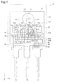
- Fig. 1 is a plan view schematically illustrating the semiconductor device in accordance with the first embodiment.
- the semiconductor device 10 illustrated in Fig. 1 is a semiconductor device of a resin seal type.
- the semiconductor device 10 comprises a plurality of semiconductor chips 14a to 14d.
- the semiconductor chips 14a to 14d may be connected in parallel.
- the semiconductor device 10 may be equipped with a die pad 12 having a chip mount surface 12a for mounting the semiconductor chips 14a to 14d.
- the die pad 12 may be electrically connected to the semiconductor chips 14a to 14d.
- the die pad 12 is formed into a plate, for example.
- the chip mount surface 12a is rectangular, for example. Examples of materials for the die pad 12 include metals such as copper (Cu) and copper alloys.
- the die pad 12 may be formed with a through hole 26 which penetrates therethrough in the thickness direction.
- the through hole 26 is a hole for inserting therethrough a screw, for example, when securing the semiconductor device 10 to another member (e.g., heatsink) with the screw.
- the semiconductor chips 14a to 14d are mounted on the chip mount surface 12a at predetermined positions.
- Examples of the semiconductor chips 14a to 14d include transistors such as bipolar transistors, MOS-FET, and insulated gate bipolar transistors (IGBT) and diodes such as pn-junction diodes and Schottky barrier diodes.
- the semiconductor chips 14a to 14d can be mounted on the chip mount surface 12a with a bonding layer constituted by a material including leaded metal solder, lead-free metal solder, a conductive resin, or the like.
- Examples of materials for the semiconductor chips 14a to 14d include wide bandgap semiconductors and other semiconductors such as silicon.
- the wide bandgap semiconductors have a bandgap greater than that of silicon. Examples of the wide bandgap semiconductors include silicon carbide (SiC), gallium nitride (GaN), and diamond.
- Each of the semiconductor chips 14a to 14d may have a gate electrode pad GP and an electrode pad SP.
- the gate electrode pad GP may be formed at an end part on a main face of the semiconductor chips 14a to 14d.
- a gate liner GL may be connected to the gate electrode pad GP.
- the electrode pad SP may be formed in a region free of the gate electrode pad GP and gate liner GL on the main face of the semiconductor chips 14a to 14d.
- the electrode pad SP corresponds to a source electrode pad.
- the electrode pad SP corresponds to an emitter electrode pad.
- the whole rear face of the semiconductor chip 14a to 14d may be formed with another electrode pad such as a drain electrode pad or collector electrode pad, for example.
- a gate wiring 30a, a first wiring 32a, and a second wiring 34a are connected to the semiconductor chip 14a.
- the gate wiring 30a may be connected to the gate electrode pad GP of the semiconductor chip 14a.
- the first wiring 32a and second wiring 34a may be connected to the electrode pad SP of the semiconductor chip 14a.
- gate wirings 30b to 30d may be connected to the gate electrode pads GP of the semiconductor chips 14b to 14d, respectively.
- First wirings 32b to 32d may be connected to the electrode pads SP of the semiconductor chips 14b to 14d, respectively.
- Second wirings 34b to 34d may be connected to the electrode pads SP of the semiconductor chips 14b to 14d, respectively.
- the first wirings 32a to 32d and second wirings 34a to 34d are wirings for supplying currents to the semiconductor chips 14b to 14d.
- the gate wirings 30a to 30d are wirings for switching the currents flowing through the first wirings 32a to 32d and second wirings 34a to 34d.
- the first wirings 32a to 32d and second wirings 34a to 34d may be arranged dispersedly on the electrode pad SP in order to inhibit currents from concentrating.
- the first wirings 32a to 32d and second wirings 34a to 34d extend along the gate wirings 30a to 30d.
- the gate wirings 30a to 30d, first wirings 32a to 32d, and second wirings 34a to 34d may extend along the XY plane.
- the first wirings 32a to 32d are arranged between the gate wirings 30a to 30d and second wirings 34a to 34d.
- the first wiring 32a is arranged between the gate wiring 30a and second wiring 34a.
- the first wirings 32a to 32d are the wirings closest to the gate wirings 30a to 30d, respectively.
- the length d1 of a first part 30x of the gate wirings 30a to 30d opposing the first wirings 32a to 32d is shorter than the length d2 of a second part 30y of the gate wirings 30a to 30d opposing the second wirings 34a to 34d.
- the length d2 may be 1.2 times or more that of the length d1.
- the lengths d1 and d2 may be measured by seeing the first wirings 32a to 32d and second wirings 34a to 34d in the Z direction perpendicular to the main faces of the semiconductor chips 14a to 14d.
- the first part 30x of the gate wirings 30a to 30d may be a part located at an intersection between the gate wirings 30a to 30d and a perpendicular drawn from a given point of the first wirings 32a to 32d to the gate wirings 30a to 30d.
- the second part 30y of the gate wirings 30a to 30d may be a part located at an intersection between the gate wirings 30a to 30d and a perpendicular drawn from a given point of the second wirings 34a to 34d to the gate wirings 30a to 30d.
- the semiconductor chips 14a to 14d may be arranged along the X direction (first direction). Arranged between the semiconductor chips 14a to 14d adjacent to each other is an axis Ax extending along the Y direction (second direction perpendicular to the first direction). With respect to the axis Ax, the gate wirings 30a to 30d, first wirings 32a to 32d, and second wirings 34a to 34d on one side may be arranged in the reverse of those on the other side. With respect to the axis Ax, the gate electrode pad GP and electrode pad SP on one side may also be arranged in the reverse of those on the other side. For example, the gate wiring 30a may be arranged at a position symmetrical to that of the gate wiring 30b with respect to the axis Ax.
- the semiconductor device 10 may comprise a first lead 18, a second lead 20, and a third lead 16.
- the leads 16, 18, 20, each extending along the Y direction, are arranged in a row along the X direction.
- the lead 16 is located between the leads 18, 20.
- the leads 16, 18, 20 and die pad 12 may construct a lead frame.
- the semiconductor device 10 is a power semiconductor device used for a power supply or the like, for example. Examples of package forms for the semiconductor device 10 include typical TO series. Examples of the TO series include TO-247, TO-220, TO-263 (D2-PAK), and TO-252 (D-PAK).
- the lead 18 is electrically connected to the gate wirings 30a to 30d.
- the lead 20 is electrically connected to the first wirings 32a to 32d and second wirings 34a to 34d.
- An inner end part of the lead 16 is mechanically integrally joined to the die pad 12. Since the die pad 12 is conductive, the lead 16 and die pad 12 are electrically connected to each other. Examples of materials for the lead 16 include the same materials as with the die pad 12.
- the leads 16, 18, and 20 correspond to drain, gate, and source electrode terminals, respectively.
- the lead 16 corresponds to a collector electrode terminal
- the lead 18 corresponds to a gate electrode terminal
- the lead 20 corresponds to an emitter electrode terminal.
- materials for the leads 18, 20 include metals such as copper and copper alloys.
- the semiconductor device 10 may comprise a wiring pattern 36 connected to the gate wirings 30a to 30d and an insulating member 38 arranged between the die pad 12 and wiring pattern 36.
- the wiring pattern 36 is connected to the lead 18 through a wiring 40.
- the insulating member 38 is interposed between the die pad 12 and wiring pattern 36 in the Z direction.
- the insulating member 38 is an insulating substrate or insulating layer, for example. Examples of materials for the insulating member 38 include resins such as epoxy resins and ceramics.
- the die pad 12, insulating member 38, and wiring pattern 36 may be bonded to one another with an adhesive.
- the semiconductor device 10 may comprise a wiring pattern 42 connected to the first wirings 32a to 32d and second wirings 34a to 34d and an insulating member 44 arranged between the die pad 12 and wiring pattern 42.
- the wiring pattern 42 is connected to the lead 20 through a plurality of wirings 46.
- the insulating member 44 is interposed between the die pad 12 and wiring pattern 42 in the Z direction.
- the insulating member 44 is an insulating substrate or insulating layer, for example. Examples of materials for the insulating member 44 include resins such as epoxy resins and ceramics.
- the die pad 12, insulating member 44, and wiring pattern 42 may be bonded to one another with an adhesive.
- the wiring patterns 36, 42 are also called wiring bars. Examples of materials for the wiring patterns 36, 42 include the same materials as with the die pad 12.
- the gate wirings 30a to 30d, first wirings 32a to 32d, second wirings 34a to 34d, and wirings 40, 46 may be wires or bonding ribbons.
- Examples of materials for the gate wirings 30a to 30d, first wirings 32a to 32d, second wirings 34a to 34d, and wirings 40, 46 include metals such as aluminum, gold, and copper.
- the gate wirings 30a to 30d, first wirings 32a to 32d, second wirings 34a to 34d, and wirings 40, 46 are connected to the wiring patterns 36, 42, semiconductor chips 14a to 14d, or leads 18, 20 by wire bonding using ultrasonic waves, pressures, or the like, for example.
- the die pad 12, semiconductor chips 14a to 14d, an inner end part of the lead 18, and an inner end part of the lead 20 may be covered with a resin part 24.
- Inner end parts of the leads 16, 18, 20 are inserted into the resin part 24.
- the parts on the inside of the resin part 24 are so-called inner lead parts.
- the parts on the outside of the resin part 24 are so-called outer lead parts.
- An example of outer forms of the resin part 24 is a substantially rectangular parallelepiped.
- materials for the resin part 24 include thermoplastic resins such as polyphenylene sulfide resins (PPS resins) and liquid crystal polymers.
- the resin part 24 may be formed by molding the die pad 12 and semiconductor chips 14a to 14d with a thermoplastic resin.
- the resin part 24 is formed with a through hole 28 whose center axis aligns with that of the through hole 26 of the die pad 12.
- the through hole 28 is a hole for inserting therethrough a screw or the like upon screwing, for example.
- the through hole 28 has a diameter smaller than that of the through hole 26.
- the gate wirings 30a to 30d are susceptible to the mutual inductances received from the first wirings 32a to 32d and second wirings 34a to 34d because of the electromagnetic effect.
- the gate voltages of the semiconductor chips 14a to 14d fluctuate with time.
- the mutual inductances are determined by the distances between the gate wirings 30a to 30d and the first wirings 32a to 32d and second wirings 34a to 34d and the lengths of the parts of the gate wirings 30a to 30d opposing the first wirings 32a to 32d and second wirings 34a to 34d.
- the mutual inductances become greater.
- the lengths of the parts of the gate wirings 30a to 30d opposing the first wirings 32a to 32d and second wirings 34a to 34d are longer, the mutual inductances become greater.
- the length d1 of the first part 30x of the gate wiring 30b opposing the first wiring 32b closest to the gate wiring 30b is shorter than the length d2 of the second part 30y of the gate wiring 30b opposing the second wiring 34b in the semiconductor device 10. Therefore, the gate wiring 30b is less susceptible to the mutual inductance received from the first wiring 32b because of the electromagnetic effect. Hence, the gate voltage is inhibited from fluctuating with time.
- the gate wirings 30a to 30d, first wirings 32a to 32d, and second wirings 34a to 34d on one side may be arranged in the reverse of those on the other side.
- fluctuations in gate voltage decrease between the semiconductor chips 14a to 14d adjacent to each other.
- the semiconductor chips 14a to 14d are made of a material containing a wide bandgap semiconductor, a greater current can flow through the first wirings 32a to 32d and second wirings 34a to 34d than in the semiconductor chips 14a to 14d made of silicon. Therefore, the gate voltage tends to fluctuate more with time in the wide bandgap semiconductor, which yields a greater effect by inhibiting the gate voltage from fluctuating with time.
- the distances between the semiconductor chips 14a to 14d and the wiring pattern 36 can be set smaller.
- the gate wirings 30a to 30d can be made shorter. This makes the gate wirings 30a to 30d less susceptible to the mutual inductances received from the first wirings 32a to 32d and second wirings 34a to 34d because of the electromagnetic effect, thereby further restraining the gate voltage from fluctuating with time.
- the semiconductor device 10 may comprise the leads 18, 20 and the die pad 12. This makes it hard to separate the gate wirings sufficiently from the first and second wirings. Therefore, the gate voltage tends to fluctuate more with time, whereby a greater effect is attained by inhibiting the gate voltage from fluctuating with time.
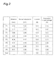
- Fig. 2 is a chart illustrating an example of fluctuations in gate voltage with time in the semiconductor device in accordance with the first embodiment.
- Fig. 2 illustrates an example of influences of the mutual inductances received by the gate wiring 30b of the semiconductor chip 14b from the first wirings 32a to 32d and second wirings 34a to 34d. The influence from the self-inductance of the gate wiring 30b is not taken into consideration.
- the current value flowing through the semiconductor chips 14a to 14d connected in parallel is 50 A. Hence, a current of 12.5 A flows through each of the semiconductor chips 14a to 14d.
- the gate voltage is 15 V.
- the switching time is 20 ns.
- the length of the gate wiring 30b is 3.2 mm.
- the length d1 of the first part 30x of the gate wiring 30b is 2.4 mm.
- the length d2 of the second part 30y of the gate wiring 30b is 3.2 mm.
- the shortest distances are the distances between the gate wiring 30b and points P1 to P8 on the first wirings 32a to 32d and second wirings 34a to 34d.
- the distance between the gate wiring 30b and the point P1 on the second wiring 34a is 3.72 mm.
- Fig. 2 illustrates results of calculations of mutual inductances and fluctuations in gate voltage.
- the mutual inductance received by the gate wiring 30b from the second wiring 34a is 0.22 nH. Its resulting fluctuation in gate voltage is 0.14 V.
- the total of mutual inductances received by the gate wiring 30b from the first wirings 32a to 32d and second wirings 34a to 34d is 1.81 nH.
- the total of fluctuations in gate voltage in the gate wiring 30b is 1.14 V (1.1 V when rounded to two significant figures).
- the mutual inductances received by the gate wiring 30a from the first wirings 32a to 32d and second wirings 34a to 34d are calculated.
- the total of mutual inductances received by the gate wiring 30a from the first wirings 32a to 32d and second wirings 34a to 34d is 1.81 nH.
- the fluctuations in gate voltage in the gate wiring 30a are also calculated.
- the total of fluctuations in gate voltage in the gate wiring 30a is 1.1 V (when rounded to two significant figures). Hence, the gate voltage incurs the same fluctuation and thus yields no variation therein between the semiconductor chips 14a, 14b adjacent to each other.
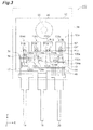
- Fig. 3 is a plan view schematically illustrating a semiconductor device for reference.
- the semiconductor device 110 illustrated in Fig. 3 has the same structure as with the semiconductor device 10 except that it comprises semiconductor chips 114a to 114d, gate wirings 130a to 130d, first wirings 132a to 132d, and second wirings 134a to 134d in place of the semiconductor chips 14a to 14d, gate wirings 30a to 30d, first wirings 32a to 32d, and second wirings 34a to 34d.
- the gate wirings 130a to 130d are arranged between the first wirings 132a to 132d and second wirings 134a to 134d. Each of parts of the gate wirings 130a to 130d opposing the first wirings 132a to 132d and second wirings 134a to 134d has the same length as with the gate wiring 130b.
- Fig. 4 is a chart illustrating an example of fluctuations in gate voltage with time in the semiconductor device for reference.
- Fig. 4 illustrates an example of influences of mutual inductances received by the gate wiring 130b of the semiconductor chip 114b from the first wirings 132a to 132d and second wirings 134a to 134d. The influence from the self-inductance of the gate wiring 130b is not taken into consideration.
- the current value flowing through the semiconductor chips 114a to 114d connected in parallel is 50 A. Hence, a current of 12.5 A flows through each of the semiconductor chips 114a to 114d.
- the gate voltage is 15 V.
- the switching time is 20 ns.
- the length of the gate wiring 130b is 3.2 mm.
- the length of the gate wiring 130b opposing the first wirings 132a to 132d and second wirings 134a to 134d is 3.2 mm.
- the shortest distances are the distances between the gate wiring 130b and points P11 to P 18 on the first wirings 132a to 132d and second wirings 134a to 134d.
- the distance between the gate wiring 130b and the point P11 on the second wiring 134a is 4.54 mm.
- the mutual inductance received by the gate wiring 130b from the second wiring 134a is 0.10 nH. Its resulting fluctuation in gate voltage is 0.07 V.
- the total of mutual inductances received by the gate wiring 130b is 1.90 nH.
- the total of fluctuations in gate voltage in the gate wiring 130b is 1.19 V (1.2 V when rounded to two significant figures).
- the mutual inductances received by the gate wiring 130a from the first wirings 132a to 132d and second wirings 134a to 134d are calculated.
- the total of mutual inductances received by the gate wiring 130a from the first wirings 132a to 132d and second wirings 134a to 134d is 1.74 nH.
- the fluctuations in gate voltage in the gate wiring 130a are also calculated.
- the total of fluctuations in gate voltage in the gate wiring 130a is 1.1 V (when rounded to two significant figures). Hence, the fluctuation in gate voltage varies by 0.1 V and thus yields a difference therein between the semiconductor chips 114a, 114b adjacent to each other.
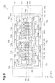
- Fig. 5 is a plan view schematically illustrating the semiconductor device in accordance with the second embodiment.
- the semiconductor device 10a illustrated in Fig. 5 is a semiconductor device of a case type.
- the semiconductor device 10a comprises semiconductor chips 14a to 141, gate wirings 30a to 301 respectively connected to the semiconductor chips 14a to 141, first wirings 32a to 321 respectively connected to the semiconductor chips 14a to 141, second wirings 34a to 341 respectively connected to the semiconductor chips 14a to 141, and a case 60.
- the semiconductor chips 14e, 14g, 14i, 14k may have the same structure as with the semiconductor chip 14a.
- the semiconductor chips 14f, 14h, 14j, 141 may have the same structure as with the semiconductor chip 14b.
- the semiconductor chips 14a to 14f are disposed on a wiring pattern 52a formed on a first substrate 50a.
- Wiring patterns 54a, 56a may be formed on the substrate 50a.
- the wiring pattern 54a may be connected to the semiconductor chips 14a to 14f through the gate wirings 30a to 30f.
- the wiring pattern 56a may be connected to the semiconductor chips 14a to 14f through the first wirings 32a to 32f and second wirings 34a to 34f.
- the semiconductor chips 14a to 14f are disposed on a wiring pattern 52b formed on a second substrate 50b.
- Wiring patterns 54b, 56b may be formed on the substrate 50b.
- the wiring pattern 54b may be connected to the semiconductor chips 14g to 141 through the gate wirings 30g to 301.
- the wiring pattern 56b may be connected to the semiconductor chips 14g to 141 through the first wirings 32g to 321 and second wirings 34g to 341.
- the case 60 may be equipped with a bottom 60a for mounting the substrates 50a, 50b.
- a table 60b for mounting bus bars 72a to 72c may be arranged on the bottom 60a.
- the bus bars 72a to 72c may be electrically connected to the semiconductor chips 14g to 141.
- the case 60 may comprise a first side wall part 60c surrounding the substrates 50a, 50b and table 60b and a second side wall part 60d surrounding the first side wall part 60c.
- the opening of the case 60 may be sealed with a lid.
- materials for the case 60 include resins such as engineering plastics typified by polybutylene terephthalate (PBT) or polyphenylene sulfide (PPS) resins.
- materials for the lid include thermoplastic resins.
- a gel such as silicone gel may be injected into the case 60 in order to mitigate stress.
- the semiconductor device 10a can attain the same operations and effects as with the semiconductor device 10.
- Fig. 6 is a plan view schematically illustrating a semiconductor device for reference.
- the semiconductor device 110a illustrated in Fig. 6 has the same structure as with the semiconductor device 10a except that it comprises semiconductor chips 114a to 1141, gate wirings 130a to 1301, first wirings 132a to 1321, and second wirings 134a to 1341 in place of the semiconductor chips 14a to 141, gate wirings 30a to 301, first wirings 32a to 321, and second wirings 34a to 341.
- the gate wirings 130a to 1301 are arranged between the first wirings 132a to 1321 and second wirings 134a to 1341. Each of parts of the gate wirings 130a to 1301 opposing the first wirings 132a to 1321 and second wirings 134a to 1341 has the same length as with the gate wiring 130b.
- the semiconductor device 10, 10a may include only one semiconductor chip.
- the semiconductor device 10, 10a may comprise a third wiring connected to the semiconductor chip.
- the semiconductor chips 14a to 141 may include lateral transistors in place of vertical transistors. In this case, no electrode pad is formed on the rear faces of the semiconductor chips 14a to 141, while different electrode pads such as drain electrode pads and collector electrode pads, for example, are formed on the front faces of the semiconductor chips 14a to 141.
- the semiconductor device 10 may be free of the wiring patterns 36, 42.
- the gate wirings 30a to 30d are connected to the lead 18.
- the first wirings 32a to 32d and second wirings 34a to 34d are connected to the lead 20.
Landscapes
- Semiconductor Integrated Circuits (AREA)
Abstract
Description
- The present invention relates to a semiconductor device.
- Known as an example of semiconductor devices is one equipped with a semiconductor chip of MOSFET (see Patent literature 1). In such a semiconductor device, a semiconductor chip mounted on a die pad is connected to a gate lead through a gate wire and to a source lead through a plurality of source wires.
- [Patent literature 1] Japanese Patent Publication No.
4746061 - In the above-mentioned semiconductor, the source wire closest to the gate wire has a length identical to or longer than that of the other source wires. Therefore, when currents flowing through a plurality of source wires vary with time, the gate wire is more susceptible to mutual inductances received from a plurality of source wires because of an electromagnetic effect. As a result, the gate voltage applied to the gate wire fluctuates more with time in the above-mentioned semiconductor device.
- It is an object of the present invention to provide a semiconductor device which can inhibit the gate voltage from fluctuating with time.
- The semiconductor device in accordance with one aspect of the present invention comprises at least one semiconductor chip, a gate wiring connected to the at least one semiconductor chip, a first wiring connected to the at least one semiconductor chip, and a second wiring connected to the at least one semiconductor chip, wherein the first and second wirings extend along the gate wiring, wherein the first wiring is arranged between the gate wiring and second wiring, wherein the first wiring is the wiring closest to the gate wiring, and wherein a first part of the gate wiring opposing the first wiring is shorter than a second part of the gate wiring opposing the second wiring. The first part of the gate wiring may be a part located at an intersection between the gate wiring and a perpendicular drawn from a given point of the first wiring to the gate wiring. The second part of the gate wiring may be a part located at an intersection between the gate wiring and a perpendicular drawn from a given point of the second wiring to the gate wiring.
- When currents flowing through the first and second wirings vary with time, the gate wiring is susceptible to mutual inductances received from the first and second wirings because of the electromagnetic effect. As a result, the gate voltage of the semiconductor chip fluctuates with time. The mutual inductances are determined by the distances between the gate wiring and the first and second wirings and the lengths of the parts of the gate wiring opposing the first and second wirings. As the distances between the gate wiring and the first and second wirings are shorter, the mutual inductances become greater. As the lengths of the parts of the gate wiring opposing the first and second wirings are longer, the mutual inductances become greater.
- In the semiconductor device, the length d1 of the first part of the gate wiring opposing the first wiring closest to the gate wiring is shorter than the length d2 of the second part of the gate wiring opposing the second wiring. Therefore, the mutual inductance received by the gate wiring from the first wiring because of the electromagnetic effect is smaller, whereby the gate voltage is inhibited from fluctuating with time.
- The at least one semiconductor chip may comprise a plurality of semiconductor chips; the plurality of semiconductor chips may be arranged along a first direction; and, with respect to an axis extending along a second direction perpendicular to the first direction between the semiconductor chips adjacent to each other, the gate wiring, first wiring, and second wiring on one side may be arranged in the reverse of those on the other side.
- This uniformizes influences of mutual inductances received by the gate wirings of semiconductor chips from the first and second wirings because of the electromagnetic effect, thereby reducing fluctuations in gate voltage between the semiconductor chips adjacent to each other.
- The at least one semiconductor chip may be made of a material containing a wide bandgap semiconductor.
- This allows a greater current to flow through the first and second wirings than in a semiconductor chip made of silicon. Therefore, the gate voltage tends to fluctuate more with time in the wide bandgap semiconductor, which yields a greater effect by inhibiting the gate voltage from fluctuating with time.
- The semiconductor device may further comprise a wiring pattern connected to the gate wiring.
- In this case, setting the distance between the semiconductor chip and the wiring pattern smaller can reduce the length of the gate wiring. This makes the gate wiring less susceptible to the mutual inductances received from the first and second wirings because of the electromagnetic effect, thereby further restraining the gate voltage from fluctuating with time.
- The semiconductor device may further comprise a first lead electrically connected to the gate wiring, a second lead electrically connected to the first and second wirings, and a die pad having a chip mount surface for mounting the at least one semiconductor chip.
- It is typically difficult for a semiconductor device equipped with a lead to separate the gate wiring sufficiently from the first and second wirings. Therefore, the gate voltage tends to fluctuate more with time in the semiconductor device equipped with the lead, which yields a greater effect by inhibiting the gate voltage from fluctuating with time.
- According to the present invention, a semiconductor device which can inhibit the gate voltage from fluctuating with time can be provided.
-
-
Fig. 1 is a plan view schematically illustrating the semiconductor device in accordance with a first embodiment; -
Fig. 2 is a chart illustrating an example of fluctuations in gate voltage with time in the semiconductor device in accordance with the first embodiment; -
Fig. 3 is a plan view schematically illustrating a semiconductor device for reference; -
Fig. 4 is a chart illustrating an example of fluctuations in gate voltage with time in the semiconductor device for reference; -
Fig. 5 is a plan view schematically illustrating the semiconductor device in accordance with a second embodiment; and -
Fig. 6 is a plan view schematically illustrating a semiconductor device for reference. - In the following, embodiments of the present invention will be explained in detail with reference to the accompanying drawings. In the explanation of the drawings, the same or equivalent constituents will be referred to with the same signs while omitting their overlapping descriptions.
Figs. 1 ,3 ,5 , and6 illustrate XYZ orthogonal coordinate systems. -
Fig. 1 is a plan view schematically illustrating the semiconductor device in accordance with the first embodiment. Thesemiconductor device 10 illustrated inFig. 1 is a semiconductor device of a resin seal type. Thesemiconductor device 10 comprises a plurality ofsemiconductor chips 14a to 14d. Thesemiconductor chips 14a to 14d may be connected in parallel. - The
semiconductor device 10 may be equipped with adie pad 12 having achip mount surface 12a for mounting thesemiconductor chips 14a to 14d. The diepad 12 may be electrically connected to thesemiconductor chips 14a to 14d. The diepad 12 is formed into a plate, for example. Thechip mount surface 12a is rectangular, for example. Examples of materials for thedie pad 12 include metals such as copper (Cu) and copper alloys. The diepad 12 may be formed with athrough hole 26 which penetrates therethrough in the thickness direction. The throughhole 26 is a hole for inserting therethrough a screw, for example, when securing thesemiconductor device 10 to another member (e.g., heatsink) with the screw. - The
semiconductor chips 14a to 14d are mounted on thechip mount surface 12a at predetermined positions. Examples of thesemiconductor chips 14a to 14d include transistors such as bipolar transistors, MOS-FET, and insulated gate bipolar transistors (IGBT) and diodes such as pn-junction diodes and Schottky barrier diodes. Thesemiconductor chips 14a to 14d can be mounted on thechip mount surface 12a with a bonding layer constituted by a material including leaded metal solder, lead-free metal solder, a conductive resin, or the like. Examples of materials for thesemiconductor chips 14a to 14d include wide bandgap semiconductors and other semiconductors such as silicon. The wide bandgap semiconductors have a bandgap greater than that of silicon. Examples of the wide bandgap semiconductors include silicon carbide (SiC), gallium nitride (GaN), and diamond. - Each of the
semiconductor chips 14a to 14d may have a gate electrode pad GP and an electrode pad SP. The gate electrode pad GP may be formed at an end part on a main face of thesemiconductor chips 14a to 14d. A gate liner GL may be connected to the gate electrode pad GP. The electrode pad SP may be formed in a region free of the gate electrode pad GP and gate liner GL on the main face of thesemiconductor chips 14a to 14d. - When the
semiconductor chips 14a to 14d include a MOS-FET, the electrode pad SP corresponds to a source electrode pad. When thesemiconductor chips 14a to 14d include an IGBT, the electrode pad SP corresponds to an emitter electrode pad. The whole rear face of thesemiconductor chip 14a to 14d may be formed with another electrode pad such as a drain electrode pad or collector electrode pad, for example. - A
gate wiring 30a, afirst wiring 32a, and asecond wiring 34a are connected to thesemiconductor chip 14a. Thegate wiring 30a may be connected to the gate electrode pad GP of thesemiconductor chip 14a. Thefirst wiring 32a andsecond wiring 34a may be connected to the electrode pad SP of thesemiconductor chip 14a. Similarly,gate wirings 30b to 30d may be connected to the gate electrode pads GP of thesemiconductor chips 14b to 14d, respectively.First wirings 32b to 32d may be connected to the electrode pads SP of thesemiconductor chips 14b to 14d, respectively. Second wirings 34b to 34d may be connected to the electrode pads SP of thesemiconductor chips 14b to 14d, respectively. Thefirst wirings 32a to 32d andsecond wirings 34a to 34d are wirings for supplying currents to thesemiconductor chips 14b to 14d. Thegate wirings 30a to 30d are wirings for switching the currents flowing through thefirst wirings 32a to 32d andsecond wirings 34a to 34d. Thefirst wirings 32a to 32d andsecond wirings 34a to 34d may be arranged dispersedly on the electrode pad SP in order to inhibit currents from concentrating. - The
first wirings 32a to 32d andsecond wirings 34a to 34d extend along thegate wirings 30a to 30d. Thegate wirings 30a to 30d,first wirings 32a to 32d, andsecond wirings 34a to 34d may extend along the XY plane. Thefirst wirings 32a to 32d are arranged between thegate wirings 30a to 30d andsecond wirings 34a to 34d. For example, thefirst wiring 32a is arranged between thegate wiring 30a andsecond wiring 34a. Thefirst wirings 32a to 32d are the wirings closest to thegate wirings 30a to 30d, respectively. The length d1 of a first part 30x of thegate wirings 30a to 30d opposing thefirst wirings 32a to 32d is shorter than the length d2 of asecond part 30y of thegate wirings 30a to 30d opposing thesecond wirings 34a to 34d. The length d2 may be 1.2 times or more that of the length d1. The lengths d1 and d2 may be measured by seeing thefirst wirings 32a to 32d andsecond wirings 34a to 34d in the Z direction perpendicular to the main faces of thesemiconductor chips 14a to 14d. The first part 30x of thegate wirings 30a to 30d may be a part located at an intersection between thegate wirings 30a to 30d and a perpendicular drawn from a given point of thefirst wirings 32a to 32d to thegate wirings 30a to 30d. Thesecond part 30y of thegate wirings 30a to 30d may be a part located at an intersection between thegate wirings 30a to 30d and a perpendicular drawn from a given point of thesecond wirings 34a to 34d to thegate wirings 30a to 30d. - The
semiconductor chips 14a to 14d may be arranged along the X direction (first direction). Arranged between thesemiconductor chips 14a to 14d adjacent to each other is an axis Ax extending along the Y direction (second direction perpendicular to the first direction). With respect to the axis Ax, thegate wirings 30a to 30d,first wirings 32a to 32d, andsecond wirings 34a to 34d on one side may be arranged in the reverse of those on the other side. With respect to the axis Ax, the gate electrode pad GP and electrode pad SP on one side may also be arranged in the reverse of those on the other side. For example, thegate wiring 30a may be arranged at a position symmetrical to that of thegate wiring 30b with respect to the axis Ax. - The
semiconductor device 10 may comprise afirst lead 18, asecond lead 20, and athird lead 16. The leads 16, 18, 20, each extending along the Y direction, are arranged in a row along the X direction. Thelead 16 is located between theleads pad 12 may construct a lead frame. Thesemiconductor device 10 is a power semiconductor device used for a power supply or the like, for example. Examples of package forms for thesemiconductor device 10 include typical TO series. Examples of the TO series include TO-247, TO-220, TO-263 (D2-PAK), and TO-252 (D-PAK). - The
lead 18 is electrically connected to thegate wirings 30a to 30d. Thelead 20 is electrically connected to thefirst wirings 32a to 32d andsecond wirings 34a to 34d. An inner end part of thelead 16 is mechanically integrally joined to thedie pad 12. Since thedie pad 12 is conductive, thelead 16 and diepad 12 are electrically connected to each other. Examples of materials for thelead 16 include the same materials as with thedie pad 12. - When the
semiconductor chips 14a to 14d include a MOS-FET, theleads semiconductor chips 14a to 14d include an IGBT, thelead 16 corresponds to a collector electrode terminal, thelead 18 corresponds to a gate electrode terminal, and thelead 20 corresponds to an emitter electrode terminal. Examples of materials for theleads - The
semiconductor device 10 may comprise awiring pattern 36 connected to thegate wirings 30a to 30d and an insulatingmember 38 arranged between thedie pad 12 andwiring pattern 36. Thewiring pattern 36 is connected to thelead 18 through awiring 40. The insulatingmember 38 is interposed between thedie pad 12 andwiring pattern 36 in the Z direction. The insulatingmember 38 is an insulating substrate or insulating layer, for example. Examples of materials for the insulatingmember 38 include resins such as epoxy resins and ceramics. Thedie pad 12, insulatingmember 38, andwiring pattern 36 may be bonded to one another with an adhesive. - The
semiconductor device 10 may comprise awiring pattern 42 connected to thefirst wirings 32a to 32d andsecond wirings 34a to 34d and an insulatingmember 44 arranged between thedie pad 12 andwiring pattern 42. Thewiring pattern 42 is connected to thelead 20 through a plurality ofwirings 46. The insulatingmember 44 is interposed between thedie pad 12 andwiring pattern 42 in the Z direction. The insulatingmember 44 is an insulating substrate or insulating layer, for example. Examples of materials for the insulatingmember 44 include resins such as epoxy resins and ceramics. Thedie pad 12, insulatingmember 44, andwiring pattern 42 may be bonded to one another with an adhesive. Thewiring patterns wiring patterns die pad 12. - The
gate wirings 30a to 30d,first wirings 32a to 32d,second wirings 34a to 34d, and wirings 40, 46 may be wires or bonding ribbons. Examples of materials for thegate wirings 30a to 30d,first wirings 32a to 32d,second wirings 34a to 34d, and wirings 40, 46 include metals such as aluminum, gold, and copper. Thegate wirings 30a to 30d,first wirings 32a to 32d,second wirings 34a to 34d, and wirings 40, 46 are connected to thewiring patterns semiconductor chips 14a to 14d, or leads 18, 20 by wire bonding using ultrasonic waves, pressures, or the like, for example. - The
die pad 12,semiconductor chips 14a to 14d, an inner end part of thelead 18, and an inner end part of thelead 20 may be covered with aresin part 24. Inner end parts of theleads resin part 24. In theleads resin part 24 are so-called inner lead parts. In theleads resin part 24 are so-called outer lead parts. An example of outer forms of theresin part 24 is a substantially rectangular parallelepiped. Examples of materials for theresin part 24 include thermoplastic resins such as polyphenylene sulfide resins (PPS resins) and liquid crystal polymers. Theresin part 24 may be formed by molding thedie pad 12 andsemiconductor chips 14a to 14d with a thermoplastic resin. Theresin part 24 is formed with a throughhole 28 whose center axis aligns with that of the throughhole 26 of thedie pad 12. As with the throughhole 26, the throughhole 28 is a hole for inserting therethrough a screw or the like upon screwing, for example. The throughhole 28 has a diameter smaller than that of the throughhole 26. - When currents flowing through the
first wirings 32a to 32d andsecond wirings 34a to 34d vary with time, thegate wirings 30a to 30d are susceptible to the mutual inductances received from thefirst wirings 32a to 32d andsecond wirings 34a to 34d because of the electromagnetic effect. As a result, the gate voltages of thesemiconductor chips 14a to 14d fluctuate with time. The mutual inductances are determined by the distances between thegate wirings 30a to 30d and thefirst wirings 32a to 32d andsecond wirings 34a to 34d and the lengths of the parts of thegate wirings 30a to 30d opposing thefirst wirings 32a to 32d andsecond wirings 34a to 34d. As the distances between thegate wirings 30a to 30d and thefirst wirings 32a to 32d andsecond wirings 34a to 34d are shorter, the mutual inductances become greater. As the lengths of the parts of thegate wirings 30a to 30d opposing thefirst wirings 32a to 32d andsecond wirings 34a to 34d are longer, the mutual inductances become greater. - For example, the length d1 of the first part 30x of the
gate wiring 30b opposing thefirst wiring 32b closest to thegate wiring 30b is shorter than the length d2 of thesecond part 30y of thegate wiring 30b opposing the second wiring 34b in thesemiconductor device 10. Therefore, thegate wiring 30b is less susceptible to the mutual inductance received from thefirst wiring 32b because of the electromagnetic effect. Hence, the gate voltage is inhibited from fluctuating with time. - With respect to the axis Ax extending along the Y direction between the
semiconductor chips 14a to 14d adjacent to each other in thesemiconductor device 10, thegate wirings 30a to 30d,first wirings 32a to 32d, andsecond wirings 34a to 34d on one side may be arranged in the reverse of those on the other side. This uniformizes influences of the mutual inductances received by thegate wirings 30a to 30d of thesemiconductor chips 14a to 14d from thefirst wirings 32a to 32d andsecond wirings 34a to 34d because of the electromagnetic effect. Hence, fluctuations in gate voltage decrease between thesemiconductor chips 14a to 14d adjacent to each other. - When the
semiconductor chips 14a to 14d are made of a material containing a wide bandgap semiconductor, a greater current can flow through thefirst wirings 32a to 32d andsecond wirings 34a to 34d than in thesemiconductor chips 14a to 14d made of silicon. Therefore, the gate voltage tends to fluctuate more with time in the wide bandgap semiconductor, which yields a greater effect by inhibiting the gate voltage from fluctuating with time. - When the
semiconductor device 10 is equipped with thewiring pattern 36 connected to thegate wirings 30a to 30d, the distances between thesemiconductor chips 14a to 14d and thewiring pattern 36 can be set smaller. As a result, thegate wirings 30a to 30d can be made shorter. This makes thegate wirings 30a to 30d less susceptible to the mutual inductances received from thefirst wirings 32a to 32d andsecond wirings 34a to 34d because of the electromagnetic effect, thereby further restraining the gate voltage from fluctuating with time. - The
semiconductor device 10 may comprise theleads die pad 12. This makes it hard to separate the gate wirings sufficiently from the first and second wirings. Therefore, the gate voltage tends to fluctuate more with time, whereby a greater effect is attained by inhibiting the gate voltage from fluctuating with time. -
Fig. 2 is a chart illustrating an example of fluctuations in gate voltage with time in the semiconductor device in accordance with the first embodiment.Fig. 2 illustrates an example of influences of the mutual inductances received by thegate wiring 30b of thesemiconductor chip 14b from thefirst wirings 32a to 32d andsecond wirings 34a to 34d. The influence from the self-inductance of thegate wiring 30b is not taken into consideration. - The current value flowing through the
semiconductor chips 14a to 14d connected in parallel is 50 A. Hence, a current of 12.5 A flows through each of thesemiconductor chips 14a to 14d. When thesemiconductor chips 14a to 14d are in operation, the gate voltage is 15 V. The switching time is 20 ns. The length of thegate wiring 30b is 3.2 mm. The length d1 of the first part 30x of thegate wiring 30b is 2.4 mm. The length d2 of thesecond part 30y of thegate wiring 30b is 3.2 mm. - As the distances between the
gate wiring 30b and thefirst wirings 32a to 32d andsecond wirings 34a to 34d, the shortest distances are employed. As illustrated inFigs. 1 and2 , the shortest distances are the distances between thegate wiring 30b and points P1 to P8 on thefirst wirings 32a to 32d andsecond wirings 34a to 34d. For example, the distance between thegate wiring 30b and the point P1 on thesecond wiring 34a is 3.72 mm. Using this distance and the lengths d1 and d2, the mutual inductances received by thegate wiring 30b from thefirst wirings 32a to 32d andsecond wirings 34a to 34d are calculated. The fluctuation V in gate voltage is calculated by the following expression:
where L is the mutual inductance, i is the current, and t is the time. -
Fig. 2 illustrates results of calculations of mutual inductances and fluctuations in gate voltage. For example, the mutual inductance received by thegate wiring 30b from thesecond wiring 34a is 0.22 nH. Its resulting fluctuation in gate voltage is 0.14 V. The total of mutual inductances received by thegate wiring 30b from thefirst wirings 32a to 32d andsecond wirings 34a to 34d is 1.81 nH. The total of fluctuations in gate voltage in thegate wiring 30b is 1.14 V (1.1 V when rounded to two significant figures). Similarly, the mutual inductances received by thegate wiring 30a from thefirst wirings 32a to 32d andsecond wirings 34a to 34d are calculated. The total of mutual inductances received by thegate wiring 30a from thefirst wirings 32a to 32d andsecond wirings 34a to 34d is 1.81 nH. The fluctuations in gate voltage in thegate wiring 30a are also calculated. The total of fluctuations in gate voltage in thegate wiring 30a is 1.1 V (when rounded to two significant figures). Hence, the gate voltage incurs the same fluctuation and thus yields no variation therein between thesemiconductor chips -
Fig. 3 is a plan view schematically illustrating a semiconductor device for reference. Thesemiconductor device 110 illustrated inFig. 3 has the same structure as with thesemiconductor device 10 except that it comprisessemiconductor chips 114a to 114d,gate wirings 130a to 130d,first wirings 132a to 132d, andsecond wirings 134a to 134d in place of thesemiconductor chips 14a to 14d,gate wirings 30a to 30d,first wirings 32a to 32d, andsecond wirings 34a to 34d. - The
gate wirings 130a to 130d are arranged between thefirst wirings 132a to 132d andsecond wirings 134a to 134d. Each of parts of thegate wirings 130a to 130d opposing thefirst wirings 132a to 132d andsecond wirings 134a to 134d has the same length as with thegate wiring 130b. -
Fig. 4 is a chart illustrating an example of fluctuations in gate voltage with time in the semiconductor device for reference.Fig. 4 illustrates an example of influences of mutual inductances received by thegate wiring 130b of thesemiconductor chip 114b from thefirst wirings 132a to 132d andsecond wirings 134a to 134d. The influence from the self-inductance of thegate wiring 130b is not taken into consideration. - The current value flowing through the
semiconductor chips 114a to 114d connected in parallel is 50 A. Hence, a current of 12.5 A flows through each of thesemiconductor chips 114a to 114d. When thesemiconductor chips 114a to 114d are in operation, the gate voltage is 15 V. The switching time is 20 ns. The length of thegate wiring 130b is 3.2 mm. The length of thegate wiring 130b opposing thefirst wirings 132a to 132d andsecond wirings 134a to 134d is 3.2 mm. - As the distances between the
gate wiring 130b and thefirst wirings 132a to 132d andsecond wirings 134a to 134d, the shortest distances are employed. As illustrated inFigs. 3 and4 , the shortest distances are the distances between thegate wiring 130b and points P11 toP 18 on thefirst wirings 132a to 132d andsecond wirings 134a to 134d. For example, the distance between thegate wiring 130b and the point P11 on thesecond wiring 134a is 4.54 mm. Using this distance and the length of thegate wiring 130b, the mutual inductances received by thegate wiring 130b from thefirst wirings 132a to 132d andsecond wirings 134a to 134d are calculated.Fig. 4 illustrates results of calculations of mutual inductances and fluctuations in gate voltage. For example, the mutual inductance received by thegate wiring 130b from thesecond wiring 134a is 0.10 nH. Its resulting fluctuation in gate voltage is 0.07 V. The total of mutual inductances received by thegate wiring 130b is 1.90 nH. The total of fluctuations in gate voltage in thegate wiring 130b is 1.19 V (1.2 V when rounded to two significant figures). Similarly, the mutual inductances received by thegate wiring 130a from thefirst wirings 132a to 132d andsecond wirings 134a to 134d are calculated. The total of mutual inductances received by thegate wiring 130a from thefirst wirings 132a to 132d andsecond wirings 134a to 134d is 1.74 nH. The fluctuations in gate voltage in thegate wiring 130a are also calculated. The total of fluctuations in gate voltage in thegate wiring 130a is 1.1 V (when rounded to two significant figures). Hence, the fluctuation in gate voltage varies by 0.1 V and thus yields a difference therein between thesemiconductor chips -
Fig. 5 is a plan view schematically illustrating the semiconductor device in accordance with the second embodiment. Thesemiconductor device 10a illustrated inFig. 5 is a semiconductor device of a case type. Thesemiconductor device 10a comprisessemiconductor chips 14a to 141,gate wirings 30a to 301 respectively connected to thesemiconductor chips 14a to 141,first wirings 32a to 321 respectively connected to thesemiconductor chips 14a to 141,second wirings 34a to 341 respectively connected to thesemiconductor chips 14a to 141, and acase 60. Thesemiconductor chips semiconductor chip 14a. Thesemiconductor chips semiconductor chip 14b. - The
semiconductor chips 14a to 14f are disposed on awiring pattern 52a formed on afirst substrate 50a.Wiring patterns substrate 50a. Thewiring pattern 54a may be connected to thesemiconductor chips 14a to 14f through thegate wirings 30a to 30f. Thewiring pattern 56a may be connected to thesemiconductor chips 14a to 14f through thefirst wirings 32a to 32f andsecond wirings 34a to 34f. - Similarly, the
semiconductor chips 14a to 14f are disposed on awiring pattern 52b formed on asecond substrate 50b.Wiring patterns substrate 50b. Thewiring pattern 54b may be connected to thesemiconductor chips 14g to 141 through thegate wirings 30g to 301. Thewiring pattern 56b may be connected to thesemiconductor chips 14g to 141 through thefirst wirings 32g to 321 andsecond wirings 34g to 341. - The
case 60 may be equipped with a bottom 60a for mounting thesubstrates bus bars 72a to 72c may be arranged on the bottom 60a. The bus bars 72a to 72c may be electrically connected to thesemiconductor chips 14g to 141. Thecase 60 may comprise a firstside wall part 60c surrounding thesubstrates side wall part 60d surrounding the firstside wall part 60c. The opening of thecase 60 may be sealed with a lid. Examples of materials for thecase 60 include resins such as engineering plastics typified by polybutylene terephthalate (PBT) or polyphenylene sulfide (PPS) resins. Examples of materials for the lid include thermoplastic resins. For example, a gel such as silicone gel may be injected into thecase 60 in order to mitigate stress. Thesemiconductor device 10a can attain the same operations and effects as with thesemiconductor device 10. -
Fig. 6 is a plan view schematically illustrating a semiconductor device for reference. Thesemiconductor device 110a illustrated inFig. 6 has the same structure as with thesemiconductor device 10a except that it comprisessemiconductor chips 114a to 1141,gate wirings 130a to 1301,first wirings 132a to 1321, andsecond wirings 134a to 1341 in place of thesemiconductor chips 14a to 141,gate wirings 30a to 301,first wirings 32a to 321, andsecond wirings 34a to 341. - The
gate wirings 130a to 1301 are arranged between thefirst wirings 132a to 1321 andsecond wirings 134a to 1341. Each of parts of thegate wirings 130a to 1301 opposing thefirst wirings 132a to 1321 andsecond wirings 134a to 1341 has the same length as with thegate wiring 130b. - The present invention is not limited to the preferred embodiments explained in detail in the foregoing.
- For example, the
semiconductor device semiconductor device - The
semiconductor chips 14a to 141 may include lateral transistors in place of vertical transistors. In this case, no electrode pad is formed on the rear faces of thesemiconductor chips 14a to 141, while different electrode pads such as drain electrode pads and collector electrode pads, for example, are formed on the front faces of thesemiconductor chips 14a to 141. - The
semiconductor device 10 may be free of thewiring patterns gate wirings 30a to 30d are connected to thelead 18. Thefirst wirings 32a to 32d andsecond wirings 34a to 34d are connected to thelead 20. - 10, 10a...semiconductor device; 14a to 141...semiconductor chip; 12...die pad; 12a...chip mount surface; 18...first lead; 20...second lead; 30a to 301...gate wiring; 30x...gate wiring first part; 30y...gate wiring second part; 32a to 321...first wiring; 34a to 341...second wiring; 36...wiring pattern; Ax...axis
Claims (5)
- A semiconductor device comprising:at least one semiconductor chip;a gate wiring connected to the at least one semiconductor chip;a first wiring connected to the at least one semiconductor chip; anda second wiring connected to the at least one semiconductor chip;wherein the first and second wirings extend along the gate wiring;wherein the first wiring is arranged between the gate wiring and second wiring;wherein the first wiring is the wiring closest to the gate wiring; andwherein a first part of the gate wiring opposing the first wiring is shorter than a second part of the gate wiring opposing the second wiring.
- The semiconductor device according to claim 1, wherein the at least one semiconductor chip comprises a plurality of semiconductor chips;
wherein the plurality of semiconductor chips are arranged along a first direction; and
wherein, with respect to an axis extending along a second direction perpendicular to the first direction between the semiconductor chips adjacent to each other, the gate wiring, first wiring, and second wiring on one side are arranged in the reverse of those on the other side. - The semiconductor device according to claim 1 or 2, wherein the at least one semiconductor chip is made of a material containing a wide bandgap semiconductor.
- The semiconductor device according to any one of claims 1 to 3, further comprising a wiring pattern connected to the gate wiring.
- The semiconductor device according to any one of claims 1 to 4, further comprising:a first lead electrically connected to the gate wiring;a second lead electrically connected to the first and second wirings; anda die pad having a chip mount surface for mounting the at least one semiconductor chip.
Applications Claiming Priority (2)
| Application Number | Priority Date | Filing Date | Title |
|---|---|---|---|
| JP2012145146A JP5991045B2 (en) | 2012-06-28 | 2012-06-28 | Semiconductor device |
| PCT/JP2013/063444 WO2014002625A1 (en) | 2012-06-28 | 2013-05-14 | Semiconductor device |
Publications (2)
| Publication Number | Publication Date |
|---|---|
| EP2869340A1 true EP2869340A1 (en) | 2015-05-06 |
| EP2869340A4 EP2869340A4 (en) | 2015-08-19 |
Family
ID=49777175
Family Applications (1)
| Application Number | Title | Priority Date | Filing Date |
|---|---|---|---|
| EP13810046.6A Ceased EP2869340A4 (en) | 2012-06-28 | 2013-05-14 | SEMICONDUCTOR DEVICE |
Country Status (5)
| Country | Link |
|---|---|
| US (1) | US9087817B2 (en) |
| EP (1) | EP2869340A4 (en) |
| JP (1) | JP5991045B2 (en) |
| CN (1) | CN104321867B (en) |
| WO (1) | WO2014002625A1 (en) |
Families Citing this family (9)
| Publication number | Priority date | Publication date | Assignee | Title |
|---|---|---|---|---|
| US20130175704A1 (en) * | 2012-01-05 | 2013-07-11 | Ixys Corporation | Discrete power transistor package having solderless dbc to leadframe attach |
| JP6374225B2 (en) | 2014-06-02 | 2018-08-15 | ルネサスエレクトロニクス株式会社 | Semiconductor device and electronic device |
| JPWO2016080016A1 (en) * | 2014-11-20 | 2017-07-13 | 株式会社島津製作所 | Photodetector |
| DE102015103667A1 (en) * | 2015-03-12 | 2016-09-15 | Infineon Technologies Bipolar Gmbh & Co. Kg | Power semiconductor module with improved bond connection structure |
| US10340811B2 (en) | 2016-11-28 | 2019-07-02 | Ford Global Technologies, Llc | Inverter switching devices with gate coils to enhance common source inductance |
| WO2018237199A1 (en) * | 2017-06-22 | 2018-12-27 | Renesas Electronics America Inc. | Solid top terminal for discrete power devices |
| JP6838243B2 (en) * | 2017-09-29 | 2021-03-03 | 日立Astemo株式会社 | Power converter |
| JP7428018B2 (en) * | 2020-03-06 | 2024-02-06 | 富士電機株式会社 | semiconductor module |
| WO2021215103A1 (en) * | 2020-04-21 | 2021-10-28 | 富士電機株式会社 | Electronic circuit and semiconductor module |
Family Cites Families (12)
| Publication number | Priority date | Publication date | Assignee | Title |
|---|---|---|---|---|
| US4907068A (en) * | 1987-01-21 | 1990-03-06 | Siemens Aktiengesellschaft | Semiconductor arrangement having at least one semiconductor body |
| JPS63224335A (en) * | 1987-03-13 | 1988-09-19 | Sharp Corp | Semiconductor integrated circuit device |
| JPH03244149A (en) * | 1990-02-21 | 1991-10-30 | Mitsubishi Electric Corp | Lead frame |
| JP4292652B2 (en) * | 1999-09-30 | 2009-07-08 | 三菱電機株式会社 | Power semiconductor module |
| JP2003110077A (en) * | 2001-10-02 | 2003-04-11 | Mitsubishi Electric Corp | Semiconductor device |
| JP2004022968A (en) * | 2002-06-19 | 2004-01-22 | Mitsubishi Electric Corp | Semiconductor device and method of manufacturing the same |
| JP3896940B2 (en) * | 2002-10-08 | 2007-03-22 | 三菱電機株式会社 | Semiconductor device |
| JP2004273749A (en) * | 2003-03-07 | 2004-09-30 | Fuji Electric Fa Components & Systems Co Ltd | Semiconductor power module |
| JP4115882B2 (en) * | 2003-05-14 | 2008-07-09 | 株式会社ルネサステクノロジ | Semiconductor device |
| US7633140B2 (en) * | 2003-12-09 | 2009-12-15 | Alpha And Omega Semiconductor Incorporated | Inverted J-lead for power devices |
| JP4746061B2 (en) | 2008-02-12 | 2011-08-10 | ルネサスエレクトロニクス株式会社 | Semiconductor device |
| KR101194609B1 (en) * | 2008-07-10 | 2012-10-25 | 미쓰비시덴키 가부시키가이샤 | Power semiconductor module |
-
2012
- 2012-06-28 JP JP2012145146A patent/JP5991045B2/en active Active
-
2013
- 2013-05-14 CN CN201380026637.1A patent/CN104321867B/en active Active
- 2013-05-14 WO PCT/JP2013/063444 patent/WO2014002625A1/en not_active Ceased
- 2013-05-14 EP EP13810046.6A patent/EP2869340A4/en not_active Ceased
- 2013-05-23 US US13/901,103 patent/US9087817B2/en active Active
Also Published As
| Publication number | Publication date |
|---|---|
| US20140001481A1 (en) | 2014-01-02 |
| JP2014011227A (en) | 2014-01-20 |
| CN104321867A (en) | 2015-01-28 |
| US9087817B2 (en) | 2015-07-21 |
| CN104321867B (en) | 2017-05-10 |
| EP2869340A4 (en) | 2015-08-19 |
| WO2014002625A1 (en) | 2014-01-03 |
| JP5991045B2 (en) | 2016-09-14 |
Similar Documents
| Publication | Publication Date | Title |
|---|---|---|
| US9087817B2 (en) | Semiconductor device including a gate wiring connected to at least one semiconductor chip | |
| JP5272191B2 (en) | Semiconductor device and manufacturing method of semiconductor device | |
| US9196577B2 (en) | Semiconductor packaging arrangement | |
| CN100524735C (en) | Semiconductor device with a plurality of transistors | |
| US10698021B2 (en) | Device including a compound semiconductor chip | |
| US9082868B2 (en) | Semiconductor component and method of manufacture | |
| KR20180077047A (en) | Semiconductor device | |
| CN109473415B (en) | SMD package with top side cooling | |
| US9899481B2 (en) | Electronic component and switch circuit | |
| EP3813106A1 (en) | Semiconductor device | |
| US20130249008A1 (en) | Semiconductor device | |
| CN114334933B (en) | Semiconductor device and corresponding method of manufacturing semiconductor device | |
| US20140210061A1 (en) | Chip arrangement and chip package | |
| CN103839913A (en) | Semiconductor Packages and Methods of Formation Thereof | |
| US12165965B2 (en) | Semiconductor device | |
| US8987880B2 (en) | Chip module and a method for manufacturing a chip module | |
| US8896114B2 (en) | Semiconductor device | |
| CN110911388B (en) | Semiconductor device | |
| US20240203808A1 (en) | Semiconductor device | |
| WO2013172139A1 (en) | Semiconductor device | |
| US11646252B2 (en) | Semiconductor device including an extension element for air cooling | |
| US20130256920A1 (en) | Semiconductor device | |
| JP2014170801A (en) | Semiconductor device | |
| US20130307131A1 (en) | Semiconductor device | |
| US11348862B2 (en) | Source electrode and connector lead with notched portions for a semiconductor package |
Legal Events
| Date | Code | Title | Description |
|---|---|---|---|
| PUAI | Public reference made under article 153(3) epc to a published international application that has entered the european phase |
Free format text: ORIGINAL CODE: 0009012 |
|
| 17P | Request for examination filed |
Effective date: 20141127 |
|
| AK | Designated contracting states |
Kind code of ref document: A1 Designated state(s): AL AT BE BG CH CY CZ DE DK EE ES FI FR GB GR HR HU IE IS IT LI LT LU LV MC MK MT NL NO PL PT RO RS SE SI SK SM TR |
|
| AX | Request for extension of the european patent |
Extension state: BA ME |
|
| RA4 | Supplementary search report drawn up and despatched (corrected) |
Effective date: 20150722 |
|
| RIC1 | Information provided on ipc code assigned before grant |
Ipc: H01L 23/495 20060101ALI20150716BHEP Ipc: H01L 25/18 20060101ALI20150716BHEP Ipc: H01L 23/48 20060101ALI20150716BHEP Ipc: H01L 23/31 20060101ALN20150716BHEP Ipc: H01L 25/07 20060101AFI20150716BHEP Ipc: H01L 21/60 20060101ALI20150716BHEP |
|
| DAX | Request for extension of the european patent (deleted) | ||
| STAA | Information on the status of an ep patent application or granted ep patent |
Free format text: STATUS: EXAMINATION IS IN PROGRESS |
|
| 17Q | First examination report despatched |
Effective date: 20190314 |
|
| REG | Reference to a national code |
Ref country code: DE Ref legal event code: R003 |
|
| STAA | Information on the status of an ep patent application or granted ep patent |
Free format text: STATUS: THE APPLICATION HAS BEEN REFUSED |
|
| 18R | Application refused |
Effective date: 20200305 |