EP2869332A1 - Method for manufacturing thin film laminated element - Google Patents
Method for manufacturing thin film laminated element Download PDFInfo
- Publication number
- EP2869332A1 EP2869332A1 EP13810224.9A EP13810224A EP2869332A1 EP 2869332 A1 EP2869332 A1 EP 2869332A1 EP 13810224 A EP13810224 A EP 13810224A EP 2869332 A1 EP2869332 A1 EP 2869332A1
- Authority
- EP
- European Patent Office
- Prior art keywords
- thin
- film
- film multilayer
- multilayer body
- photosensitive resist
- Prior art date
- Legal status (The legal status is an assumption and is not a legal conclusion. Google has not performed a legal analysis and makes no representation as to the accuracy of the status listed.)
- Granted
Links
Images








Classifications
-
- H—ELECTRICITY
- H10—SEMICONDUCTOR DEVICES; ELECTRIC SOLID-STATE DEVICES NOT OTHERWISE PROVIDED FOR
- H10P—GENERIC PROCESSES OR APPARATUS FOR THE MANUFACTURE OR TREATMENT OF DEVICES COVERED BY CLASS H10
- H10P76/00—Manufacture or treatment of masks on semiconductor bodies, e.g. by lithography or photolithography
- H10P76/20—Manufacture or treatment of masks on semiconductor bodies, e.g. by lithography or photolithography of masks comprising organic materials
- H10P76/204—Manufacture or treatment of masks on semiconductor bodies, e.g. by lithography or photolithography of masks comprising organic materials of organic photoresist masks
-
- G—PHYSICS
- G03—PHOTOGRAPHY; CINEMATOGRAPHY; ANALOGOUS TECHNIQUES USING WAVES OTHER THAN OPTICAL WAVES; ELECTROGRAPHY; HOLOGRAPHY
- G03F—PHOTOMECHANICAL PRODUCTION OF TEXTURED OR PATTERNED SURFACES, e.g. FOR PRINTING, FOR PROCESSING OF SEMICONDUCTOR DEVICES; MATERIALS THEREFOR; ORIGINALS THEREFOR; APPARATUS SPECIALLY ADAPTED THEREFOR
- G03F9/00—Registration or positioning of originals, masks, frames, photographic sheets or textured or patterned surfaces, e.g. automatically
- G03F9/70—Registration or positioning of originals, masks, frames, photographic sheets or textured or patterned surfaces, e.g. automatically for microlithography
- G03F9/7073—Alignment marks and their environment
- G03F9/7076—Mark details, e.g. phase grating mark, temporary mark
-
- H—ELECTRICITY
- H01—ELECTRIC ELEMENTS
- H01G—CAPACITORS; CAPACITORS, RECTIFIERS, DETECTORS, SWITCHING DEVICES, LIGHT-SENSITIVE OR TEMPERATURE-SENSITIVE DEVICES OF THE ELECTROLYTIC TYPE
- H01G4/00—Fixed capacitors; Processes of their manufacture
- H01G4/002—Details
- H01G4/018—Dielectrics
- H01G4/06—Solid dielectrics
- H01G4/08—Inorganic dielectrics
- H01G4/12—Ceramic dielectrics
-
- G—PHYSICS
- G03—PHOTOGRAPHY; CINEMATOGRAPHY; ANALOGOUS TECHNIQUES USING WAVES OTHER THAN OPTICAL WAVES; ELECTROGRAPHY; HOLOGRAPHY
- G03F—PHOTOMECHANICAL PRODUCTION OF TEXTURED OR PATTERNED SURFACES, e.g. FOR PRINTING, FOR PROCESSING OF SEMICONDUCTOR DEVICES; MATERIALS THEREFOR; ORIGINALS THEREFOR; APPARATUS SPECIALLY ADAPTED THEREFOR
- G03F7/00—Photomechanical, e.g. photolithographic, production of textured or patterned surfaces, e.g. printing surfaces; Materials therefor, e.g. comprising photoresists; Apparatus specially adapted therefor
- G03F7/20—Exposure; Apparatus therefor
-
- G—PHYSICS
- G03—PHOTOGRAPHY; CINEMATOGRAPHY; ANALOGOUS TECHNIQUES USING WAVES OTHER THAN OPTICAL WAVES; ELECTROGRAPHY; HOLOGRAPHY
- G03F—PHOTOMECHANICAL PRODUCTION OF TEXTURED OR PATTERNED SURFACES, e.g. FOR PRINTING, FOR PROCESSING OF SEMICONDUCTOR DEVICES; MATERIALS THEREFOR; ORIGINALS THEREFOR; APPARATUS SPECIALLY ADAPTED THEREFOR
- G03F9/00—Registration or positioning of originals, masks, frames, photographic sheets or textured or patterned surfaces, e.g. automatically
- G03F9/70—Registration or positioning of originals, masks, frames, photographic sheets or textured or patterned surfaces, e.g. automatically for microlithography
- G03F9/7073—Alignment marks and their environment
- G03F9/708—Mark formation
-
- H—ELECTRICITY
- H01—ELECTRIC ELEMENTS
- H01G—CAPACITORS; CAPACITORS, RECTIFIERS, DETECTORS, SWITCHING DEVICES, LIGHT-SENSITIVE OR TEMPERATURE-SENSITIVE DEVICES OF THE ELECTROLYTIC TYPE
- H01G4/00—Fixed capacitors; Processes of their manufacture
- H01G4/33—Thin- or thick-film capacitors (thin- or thick-film circuits; capacitors without a potential-jump or surface barrier specially adapted for integrated circuits, details thereof, multistep manufacturing processes therefor)
-
- H—ELECTRICITY
- H10—SEMICONDUCTOR DEVICES; ELECTRIC SOLID-STATE DEVICES NOT OTHERWISE PROVIDED FOR
- H10D—INORGANIC ELECTRIC SEMICONDUCTOR DEVICES
- H10D1/00—Resistors, capacitors or inductors
- H10D1/60—Capacitors
- H10D1/68—Capacitors having no potential barriers
- H10D1/692—Electrodes
- H10D1/711—Electrodes having non-planar surfaces, e.g. formed by texturisation
-
- H—ELECTRICITY
- H10—SEMICONDUCTOR DEVICES; ELECTRIC SOLID-STATE DEVICES NOT OTHERWISE PROVIDED FOR
- H10D—INORGANIC ELECTRIC SEMICONDUCTOR DEVICES
- H10D1/00—Resistors, capacitors or inductors
- H10D1/60—Capacitors
- H10D1/68—Capacitors having no potential barriers
- H10D1/692—Electrodes
-
- H—ELECTRICITY
- H10—SEMICONDUCTOR DEVICES; ELECTRIC SOLID-STATE DEVICES NOT OTHERWISE PROVIDED FOR
- H10P—GENERIC PROCESSES OR APPARATUS FOR THE MANUFACTURE OR TREATMENT OF DEVICES COVERED BY CLASS H10
- H10P50/00—Etching of wafers, substrates or parts of devices
- H10P50/73—Etching of wafers, substrates or parts of devices using masks for insulating materials
Definitions
- the present invention relates to a method for producing a thin-film multilayer device that functions as a thin-film capacitor or the like.
- the downward progress method disclosed in Prior Document 1 begins with, as illustrated in Fig. 22 (A) , forming a thin-film multilayer body 107 having multiple thin films 103, 104, 105, and 106 that function as components such as capacitor electrodes. Then photolithographic etching is repeated multiple times to perform processing on predetermined ones of the thin films 103, 104, 105, and 106 of the thin-film multilayer body 107 sequentially from the surface.
- the downward progress method disclosed in Prior Document 1 includes forming multiple alignment marks 131 on the uppermost layer of the thin-film multilayer body 107 through photolithographic etching beforehand as illustrated in Fig. 22 (B) so that the thin-film multilayer body 107 is etched with high positional accuracy. These multiple alignment marks 131 are used to position a photomask in any of the repeated rounds of etching.
- any unnecessary alignment mark 131 which is not to be used in that round of etching, has to be covered with a photosensitive resist for protection against damage associated with etching. This means that a photosensitive resist is repeatedly applied to and detached from the alignment marks 131 that are used in later rounds of repeated etching.
- Patent Document 1 Japanese Unexamined Patent Application Publication No. 2010-21478
- This known production method however, often causes damage to the alignment marks 131 because in this method a photosensitive resist is applied to and detached from the same alignment marks 131 many times.
- the use of damaged alignment marks 131 causes a large misalignment between the correct position and the recognized one, leading to reduced accuracy in the processing of the thin-film multilayer body 107.
- An object of the present invention is therefore to provide a method for producing a thin-film multilayer device, the method allowing the user to position a photomask for etching using a less-damaged alignment mark.
- a method for producing a thin-film multilayer device include a first process having a step of forming a thin-film multilayer body having a plurality of thin films, a second process having a step of applying a photosensitive resist to the thin-film multilayer body, a step of exposing the resist through a photomask and developing the exposed resist, a step of etching the thin-film multilayer body coated with the developed photosensitive resist to form a device section and an alignment mark on the thin-film multilayer body, and a step of removing the photosensitive resist from the etched thin-film multilayer body, and a third process having a step of applying a photosensitive resist to the thin-film multilayer body, a step of placing a photomask having an alignment pattern in position on the photosensitive resist by aligning the alignment pattern with the alignment mark formed in a previous process, a step of exposing the photosensitive resist through the photomask and developing the exposed photosensitive resist, a step of etching the thin-film
- the approach of forming a thin-film multilayer body while forming alignment marks one by one allows the tolerance setting for the misalignments of the alignment marks to be smaller.
- Known devices whose functionality depends on the size of the area where the incorporated conductors, such as capacitors, overlap require the conductors have a large size in the initial design so that the functionality does not fall below the tolerance even with the occurrence of a misalignment, and this has on occasion caused the devices to be large in size.
- a production method according to the present invention allows the user to obtain the desired functionality without increasing the size and, furthermore, allows the user to reduce the size of a device without compromising its functionality.
- Fig. 21 illustrates a thin-film multilayer device 100 that functions as a thin-film capacitor, providing an example of a thin-film multilayer device produced using a method according to this embodiment for producing a thin-film multilayer device.
- the thin-film multilayer device 100 has a substrate 1 made of Si, the substrate having a Si thermal oxide film 2 made of SiO 2 on its surface.
- a dielectric thin film 3 is disposed that functions as an adhesion layer and is made of (Ba, Sr)TiO 3 (hereinafter referred to as BST).
- BST a dielectric thin film 3
- a conductive thin film 4 is disposed that functions as a capacitor electrode and is made of Pt.
- a dielectric thin film 5 is disposed that functions as a capacitor dielectric and is made of BST.
- a dielectric thin film 5 is disposed that functions as a protective layer and is made of BST.
- the thin-film multilayer body 7 has a device section 10 that functions as a thin-film capacitor.
- An inorganic protective film 12 made of SiO 2 for enhancing moisture resistance and an organic protective film 13 for buffering external forces are disposed around the device section 10.
- An outer electrode 14 is disposed on the organic protective film 13 so as to be connected to a predetermined point on the conductive thin films 4 as capacitor electrodes.
- the outer electrode 14 is made up of a Ti thin film, a Ni thin film, and a Au thin film stacked in this order (not illustrated).
- the following describes a method according to an embodiment of the present invention for producing the thin-film multilayer device 100.
- a thin-film multilayer body 7 is formed on a substrate 1 having a thermal oxide film 2 on its surface.
- a substrate 1 is provided that is made of Si and has a Si thermal oxide film 2 made of SiO 2 on its surface.
- the thickness of the thermal oxide film 2 is, for example, 700 nm, and the thickness of the substrate 1 is, for example, 0.5 mm.
- a dielectric thin film 3 made of BST is formed on the thermal oxide film 2 using metal organic deposition (MOD).
- MOD metal organic deposition
- the thickness of the dielectric thin film 3 is, for example, 100 nm.
- a conductive thin film 4 made of Pt is formed using sputtering.
- the thickness of the conductive thin film 4 is, for example, 200 nm.
- a step of alternately forming a dielectric thin film 5 made of BST and a conductive thin film 4 made of Pt in the way described above is performed four times.
- a dielectric thin film 6 made of BST is formed.
- a thin-film multilayer body 7 made up of a dielectric thin film 3, multiple conductive thin films 4, multiple dielectric thin films 5, and a dielectric thin film 6 is formed on a substrate 1 having a thermal oxide film 2 on its surface.
- an alignment mark 31a to be used in a third process is formed on the surface of the thin-film multilayer body 7.
- a positive photosensitive resist 8 is applied to the dielectric thin film 6 using spin coating and then baked.
- a photomask 9a having a device-section pattern 11a and an alignment pattern 21a is placed on the photosensitive resist 8.
- the alignment pattern 21a is made up of four square elements arranged at certain intervals.
- the photosensitive resist 8 is exposed through the photomask 9a, and then the photomask 9a is removed. As a result, the photosensitive resist 8 has an unexposed portion 8a and an exposed portion 8b as illustrated in Figs. 5 (A) and (B) .
- the dielectric thin film 6 coated with the photosensitive resist 8 and a conductive thin film 4 are processed together using RIE (reactive ion etching), forming a device section 10 and creating an alignment mark 31a on a portion of the surface of the thin-film multilayer body 7.
- RIE reactive ion etching
- the photosensitive resist 8 is removed from the thin-film multilayer body 7 using O 2 plasma ashing.
- an alignment mark 31a to be used in the next process and a device section 10 are completed on a portion of the surface of the thin-film multilayer body 7.
- etching is performed through a photomask positioned using the alignment mark 31a formed in the second process.
- the thin-film multilayer body 7 is processed from its surface, further forming the device section 10 and creating a new alignment mark.
- a positive photosensitive resist 8 is applied to the surface of the thin-film multilayer body 7 using spin coating and then baked.
- a photomask 9b having a device-section pattern 11b, an alignment pattern 21b, and a cruciform alignment pattern 41a is placed on the photosensitive resist 8.
- the photomask 9b is placed in position on the photosensitive resist 8 through the alignment of the cruciform alignment pattern 41a with the alignment mark 31a, which is formed on the surface of the thin-film multilayer body 7 in the previous process.
- the photosensitive resist 8 is exposed through the photomask 9b, and the photomask 9b is removed.
- the photosensitive resist 8 has an unexposed portion 8a and an exposed portion 8b as illustrated in Figs. 11 (A) and (B) .
- the dielectric thin film 6 coated with the photosensitive resist and a conductive thin film 4 are processed together using RIE, further forming the device section 10 and creating a new alignment mark 31b on the thin-film multilayer body 7.
- the photosensitive resist 8 is removed from the thin-film multilayer body 7 using O 2 plasma ashing.
- the above third process is repeated multiple times to process the thin-film multilayer body 7 sequentially from its surface, thereby further forming the device section 10.
- a photomask is positioned using an alignment mark formed in the previous third process.
- the above third process is repeated using the new alignment mark 31b to position a photomask (not illustrated), further forming the device section 10 and creating an alignment mark 31c to be used in the next process on the thin-film multilayer body 7 as illustrated in Figs. 15 (A) and (B) .
- the above third process is repeated using the new alignment mark 31c to position a photomask (not illustrated), further forming the device section 10 and creating an alignment mark 31d to be used in the next process on the thin-film multilayer body 7 as illustrated in Figs. 16 (A) and (B) .
- the above third process is repeated using the new alignment mark 31d to position a photomask (not illustrated), further forming the device section 10 and creating an alignment mark 31e to be used in the next process on the thin-film multilayer body 7 as illustrated in Figs. 17 (A) and (B) .
- the thin-film multilayer device 100 is completed through the formation of an inorganic protective film 12 made of SiO 2 and an organic protective film 13, which both surround the device section 10, and an outer electrode 14 connected to a portion of the conductive thin films 4 as capacitor electrodes.
- the entire thin-film multilayer body 7 including the device section 10 is subjected to a heat treatment at approximately 850°C.
- an inorganic protective film 12 made of SiO 2 is formed using chemical vapor deposition (CVD).
- an organic protective film 13 that functions as a positive photosensitive resist is applied using spin coating.
- the thickness of the inorganic protective film 12 is, for example, 700 nm, and the thickness of the organic protective film 13 is, for example, 5000 nm.
- a photomask 9f having an alignment pattern 21f is placed in position on the organic protective film 13 through, as in the second process, the alignment of a cruciform alignment pattern 41e created in the photomask 9f with the alignment mark 31e formed in the previous process.
- the positive organic protective film 13 is exposed through the photomask 9f having the alignment pattern 21f and then developed to pattern the organic protective film 13.
- the inorganic protective film 12 and the dielectric thin films 5 are together dry-etched with CHF 3 gas using the patterned organic protective film 13 as a mask to expose a portion of the conductive thin films 4 as capacitor electrodes.
- a new alignment mark 31f is also created.
- an outer electrode 14 is formed so as to be connected to a portion of the conducive thin films 4 as capacitor electrodes of the device section 10 through sputtering using the alignment mark 31f, completing the thin-film multilayer device 100.
- a Ti thin film, a Ni thin film, and a Au thin film are sequentially formed using sputtering.
- the thickness of the Ti thin film is, for example, 50 nm
- the thickness of the Ni thin film is, for example, 1000 nm
- the thickness of the Au thin film is, for example, 200 nm.
- a positive photosensitive resist (not illustrated) is applied using spin coating.
- an alignment pattern created in a photomask (not illustrated) is aligned with the alignment mark 31f, and this photomask is used to form a pattern corresponding to the outer electrode 14 in the photosensitive resist.
- the layer made up of the Ti thin film, the Ni thin film, and the Au thin film and masked with the photosensitive resist is processed using RIE, forming an outer electrode 14 connected to a portion of the conductive thin films 4 as capacitor electrodes.
- the photosensitive resist 8 is removed using O 2 plasma ashing to complete a patterned outer electrode 14.
- Methods according to an embodiment of the present invention for producing a thin-film multilayer device are not limited to the above, and various modifications can be made without departing from the gist of the invention.
- the third process which is repeated multiple times in the production method according to the above embodiment, may be performed once.
- the photosensitive resists which are positive ones in the above embodiment, may be negative ones.
- the number of layers etched together in each round of etching, which is one conductive thin film and one dielectric thin film in the above embodiment, is not limited.
- the alignment marks created in the thin-film multilayer body and the alignment pattern of the photomasks may have any shape that allows for accurate alignment for etching.
Landscapes
- Engineering & Computer Science (AREA)
- Power Engineering (AREA)
- Microelectronics & Electronic Packaging (AREA)
- Physics & Mathematics (AREA)
- General Physics & Mathematics (AREA)
- Chemical & Material Sciences (AREA)
- Manufacturing & Machinery (AREA)
- Ceramic Engineering (AREA)
- Inorganic Chemistry (AREA)
- Fixed Capacitors And Capacitor Manufacturing Machines (AREA)
- Exposure And Positioning Against Photoresist Photosensitive Materials (AREA)
- Exposure Of Semiconductors, Excluding Electron Or Ion Beam Exposure (AREA)
Abstract
Description
- The present invention relates to a method for producing a thin-film multilayer device that functions as a thin-film capacitor or the like.
- An example of a known method for producing a thin-film multilayer device is a downward progress method disclosed in Prior Document 1 (Japanese Unexamined Patent Application Publication No.
2010-21478 - The downward progress method disclosed in
Prior Document 1 begins with, as illustrated inFig. 22 (A) , forming a thin-film multilayer body 107 having multiplethin films thin films film multilayer body 107 sequentially from the surface. - The downward progress method disclosed in
Prior Document 1 includes formingmultiple alignment marks 131 on the uppermost layer of the thin-film multilayer body 107 through photolithographic etching beforehand as illustrated inFig. 22 (B) so that the thin-film multilayer body 107 is etched with high positional accuracy. Thesemultiple alignment marks 131 are used to position a photomask in any of the repeated rounds of etching. - In each round of etching, any
unnecessary alignment mark 131, which is not to be used in that round of etching, has to be covered with a photosensitive resist for protection against damage associated with etching. This means that a photosensitive resist is repeatedly applied to and detached from thealignment marks 131 that are used in later rounds of repeated etching. - Patent Document 1: Japanese Unexamined Patent Application Publication No.
2010-21478 - This known production method, however, often causes damage to the
alignment marks 131 because in this method a photosensitive resist is applied to and detached from thesame alignment marks 131 many times. The use of damagedalignment marks 131 causes a large misalignment between the correct position and the recognized one, leading to reduced accuracy in the processing of the thin-film multilayer body 107. - An object of the present invention is therefore to provide a method for producing a thin-film multilayer device, the method allowing the user to position a photomask for etching using a less-damaged alignment mark.
- To achieve this object, a method according to the present invention for producing a thin-film multilayer device include a first process having a step of forming a thin-film multilayer body having a plurality of thin films, a second process having a step of applying a photosensitive resist to the thin-film multilayer body, a step of exposing the resist through a photomask and developing the exposed resist, a step of etching the thin-film multilayer body coated with the developed photosensitive resist to form a device section and an alignment mark on the thin-film multilayer body, and a step of removing the photosensitive resist from the etched thin-film multilayer body, and a third process having a step of applying a photosensitive resist to the thin-film multilayer body, a step of placing a photomask having an alignment pattern in position on the photosensitive resist by aligning the alignment pattern with the alignment mark formed in a previous process, a step of exposing the photosensitive resist through the photomask and developing the exposed photosensitive resist, a step of etching the thin-film multilayer body coated with the developed photosensitive resist to form a device section and an alignment mark on the thin-film multilayer body, and a step of removing the photosensitive resist from the etched thin-film multilayer body.
- According to a method according to the present invention for producing a thin-film multilayer device, reduced damage to alignment marks and a reduced misalignment between the correct position and the recognized one lead to enhanced accuracy in the processing of a thin-film multilayer body.
- Furthermore, the approach of forming a thin-film multilayer body while forming alignment marks one by one allows the tolerance setting for the misalignments of the alignment marks to be smaller. Known devices whose functionality depends on the size of the area where the incorporated conductors, such as capacitors, overlap require the conductors have a large size in the initial design so that the functionality does not fall below the tolerance even with the occurrence of a misalignment, and this has on occasion caused the devices to be large in size. A production method according to the present invention allows the user to obtain the desired functionality without increasing the size and, furthermore, allows the user to reduce the size of a device without compromising its functionality.
-
- [
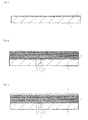
Fig. 1] Fig. 1 is a cross-sectional view that illustrates a process used in a method according to an embodiment of the invention for producing a thin-film multilayer device 100. - [
Fig. 2] Fig. 2 , a continuation ofFig. 1 , is a cross-sectional view that illustrates a process used in a method according to an embodiment of the invention for producing a thin-film multilayer device 100. - [
Fig. 3] Fig. 3 , a continuation ofFig. 2 , is a cross-sectional view that illustrates a process used in a method according to an embodiment of the invention for producing a thin-film multilayer device 100. - [
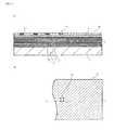
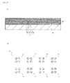
Fig. 4] Fig. 4 , a continuation ofFig. 3 , illustrates a process used in a method according to an embodiment of the invention for producing a thin-film multilayer device 100.Fig. 4 (A) is a cross-sectional view taken along line A-A, andFig. 4 (B) is a plan view with some details omitted. - [
Fig. 5] Fig. 5 , a continuation ofFig. 4 , illustrates a process used in a method according to an embodiment of the invention for producing a thin-film multilayer device 100.Fig. 5 (A) is a cross-sectional view taken along line A-A, andFig. 5 (B) is a plan view with some details omitted. - [
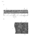
Fig. 6] Fig. 6 , a continuation ofFig. 5 , illustrates a process used in a method according to an embodiment of the invention for producing a thin-film multilayer device 100.Fig. 6 (A) is a cross-sectional view taken along line A-A, andFig. 6 (B) is a plan view with some details omitted. - [
Fig. 7] Fig. 7 , a continuation ofFig. 6 , illustrates a process used in a method according to an embodiment of the invention for producing a thin-film multilayer device 100.Fig. 7 (A) is a cross-sectional view taken along line A-A, andFig. 7 (B) is a plan view with some details omitted. - [
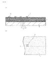
Fig. 8] Fig. 8 , a continuation ofFig. 7 , illustrates a process used in a method according to an embodiment of the invention for producing a thin-film multilayer device 100.Fig. 8 (A) is a cross-sectional view taken along line A-A, andFig. 8 (B) is a plan view with some details omitted. - [
Fig. 9] Fig. 9 , a continuation ofFig. 8 , illustrates a process used in a method according to an embodiment of the invention for producing a thin-film multilayer device 100.Fig. 9 (A) is a cross-sectional view taken along line A-A, andFig. 9 (B) is a plan view with some details omitted. - [
Fig. 10] Fig. 10 , a continuation ofFig. 9 , illustrates a process used in a method according to an embodiment of the invention for producing a thin-film multilayer device 100.Fig. 10 (A) is a cross-sectional view taken along line A-A, andFig. 10 (B) is a plan view with some details omitted. - [
Fig. 11] Fig. 11 , a continuation ofFig. 10 , illustrates a process used in a method according to an embodiment of the invention for producing a thin-film multilayer device 100.Fig. 11 (A) is a cross-sectional view taken along line A-A, andFig. 11 (B) is a plan view with some details omitted. - [
Fig. 12] Fig. 12 , a continuation ofFig. 11 , illustrates a process used in a method according to an embodiment of the invention for producing a thin-film multilayer device 100.Fig. 12 (A) is a cross-sectional view taken along line A-A, andFig. 12 (B) is a plan view with some details omitted. - [
Fig. 13] Fig. 13 , a continuation ofFig. 12 , illustrates a process used in a method according to an embodiment of the invention for producing a thin-film multilayer device 100.Fig. 13 (A) is a cross-sectional view taken along line A-A, andFig. 13 (B) is a plan view with some details omitted. - [
Fig. 14] Fig. 14 , a continuation ofFig. 13 , illustrates a process used in a method according to an embodiment of the invention for producing a thin-film multilayer device 100.Fig. 14 (A) is a cross-sectional view taken along line A-A, andFig. 14 (B) is a plan view with some details omitted. - [
Fig. 15] Fig. 15 , a continuation ofFig. 14 , illustrates a process used in a method according to an embodiment of the invention for producing a thin-film multilayer device 100.Fig. 15 (A) is a cross-sectional view taken along line A-A, andFig. 15 (B) is a plan view with some details omitted. - [
Fig. 16] Fig. 16 , a continuation ofFig. 15 , illustrates a process used in a method according to an embodiment of the invention for producing a thin-film multilayer device 100.Fig. 16 (A) is a across-sectional view taken along line A-A, andFig. 16 (B) is a plan view with some details omitted. - [
Fig. 17] Fig. 17 , a continuation ofFig. 16 , illustrates a process used in a method according to an embodiment of the invention for producing a thin-film multilayer device 100.Fig. 17 (A) is a cross-sectional view taken along line A-A, andFig. 17 (B) is a plan view with some details omitted. - [
Fig. 18] Fig. 18 , a continuation ofFig. 17 , illustrates a process used in a method according to an embodiment of the invention for producing a thin-film multilayer device 100.Fig. 18 (A) is a cross-sectional view taken along line A-A, andFig. 18 (B) is a plan view with some details omitted. - [
Fig. 19] Fig. 19 , a continuation ofFig. 18 , illustrates a process used in a method according to an embodiment of the invention for producing a thin-film multilayer device 100.Fig. 19 (A) is a across-sectional view taken along line A-A, andFig. 19 (B) is a plan view with some details omitted. - [
Fig. 20] Fig. 20 , a continuation ofFig. 19 , illustrates a process used in a method according to an embodiment of the invention for producing a thin-film multilayer device 100.Fig. 20 (A) is a cross-sectional view taken along line A-A, andFig. 20 (B) is a plan view with some details omitted. - [
Fig. 21] Fig. 21 , a continuation ofFig. 20 , illustrates a process used in a method according to an embodiment of the invention for producing a thin-film multilayer device 100.Fig. 21 (A) is a cross-sectional view taken along line A-A, andFig. 21 (B) is a plan view with some details omitted.Fig. 21 is also an illustration of the finished structure of the thin-film multilayer device 100 according to an embodiment of the invention. - [
Fig. 22] Fig. 22 illustrates a known method for producing a thin-film multilayer device.Fig. 22 (A) is a cross-sectional view of a thin-film multilayer body 107, andFig. 22 (B) is a plan view of alignment marks 131 formed on the uppermost layer of the thin-film multilayer body 107. Description of Embodiments - The following describes an embodiment of the present invention with reference to drawings.
-
Fig. 21 illustrates a thin-film multilayer device 100 that functions as a thin-film capacitor, providing an example of a thin-film multilayer device produced using a method according to this embodiment for producing a thin-film multilayer device. - The thin-
film multilayer device 100 has asubstrate 1 made of Si, the substrate having a Sithermal oxide film 2 made of SiO2 on its surface. - On the
thermal oxide film 2, a dielectricthin film 3 is disposed that functions as an adhesion layer and is made of (Ba, Sr)TiO3 (hereinafter referred to as BST). On thedielectric film 3, a conductivethin film 4 is disposed that functions as a capacitor electrode and is made of Pt. On the conductivethin film 4, a dielectricthin film 5 is disposed that functions as a capacitor dielectric and is made of BST. On the dielectricthin film 5, as many pairs of a conductivethin film 4 and a dielectricthin film 5 as needed are disposed. On the uppermost conductivethin film 4, a dielectricthin film 6 is disposed that functions as a protective layer and is made of BST. These thin films, i.e., a dielectricthin film 3, multiple conductivethin films 4, multiple dielectricthin films 5, and a dielectricthin film 6, make up a thin-film multilayer body 7. - The thin-
film multilayer body 7 has adevice section 10 that functions as a thin-film capacitor. - An inorganic
protective film 12 made of SiO2 for enhancing moisture resistance and an organicprotective film 13 for buffering external forces are disposed around thedevice section 10. - An
outer electrode 14 is disposed on the organicprotective film 13 so as to be connected to a predetermined point on the conductivethin films 4 as capacitor electrodes. Theouter electrode 14 is made up of a Ti thin film, a Ni thin film, and a Au thin film stacked in this order (not illustrated). - The following describes a method according to an embodiment of the present invention for producing the thin-
film multilayer device 100. - In a first process, a thin-
film multilayer body 7 is formed on asubstrate 1 having athermal oxide film 2 on its surface. - First, as illustrated in
Fig. 1 , asubstrate 1 is provided that is made of Si and has a Sithermal oxide film 2 made of SiO2 on its surface. The thickness of thethermal oxide film 2 is, for example, 700 nm, and the thickness of thesubstrate 1 is, for example, 0.5 mm. - Then as illustrated in
Fig. 2 , a dielectricthin film 3 made of BST is formed on thethermal oxide film 2 using metal organic deposition (MOD). The thickness of the dielectricthin film 3 is, for example, 100 nm. On this dielectricthin film 3, a conductivethin film 4 made of Pt is formed using sputtering. The thickness of the conductivethin film 4 is, for example, 200 nm. On thisconductive film 4, a step of alternately forming a dielectricthin film 5 made of BST and a conductivethin film 4 made of Pt in the way described above is performed four times. Lastly, a dielectricthin film 6 made of BST is formed. - Through these steps, a thin-
film multilayer body 7 made up of a dielectricthin film 3, multiple conductivethin films 4, multiple dielectricthin films 5, and a dielectricthin film 6 is formed on asubstrate 1 having athermal oxide film 2 on its surface. - In a second process, an
alignment mark 31a to be used in a third process, which follows this second process, is formed on the surface of the thin-film multilayer body 7. - First, as illustrated in
Fig. 3 , a positive photosensitive resist 8 is applied to the dielectricthin film 6 using spin coating and then baked. - Then as illustrated in
Figs. 4 (A) and (B) , aphotomask 9a having a device-section pattern 11a and analignment pattern 21a is placed on the photosensitive resist 8. Thealignment pattern 21a is made up of four square elements arranged at certain intervals. - The photosensitive resist 8 is exposed through the
photomask 9a, and then thephotomask 9a is removed. As a result, the photosensitive resist 8 has anunexposed portion 8a and an exposedportion 8b as illustrated inFigs. 5 (A) and (B) . - Then as illustrated in
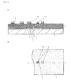
Figs. 6 (A) and (B) , theunexposed portion 8b of the photosensitive resist 8 is removed through development, forming a patterned photosensitive resist 8 on the thin-film multilayer body 7. - Then as illustrated in
Figs. 7 (A) and (B) , the dielectricthin film 6 coated with the photosensitive resist 8 and a conductivethin film 4 are processed together using RIE (reactive ion etching), forming adevice section 10 and creating analignment mark 31a on a portion of the surface of the thin-film multilayer body 7. - Then as illustrated in
Figs. 8 (A) and (B) , the photosensitive resist 8 is removed from the thin-film multilayer body 7 using O2 plasma ashing. - Through these steps, an
alignment mark 31a to be used in the next process and adevice section 10 are completed on a portion of the surface of the thin-film multilayer body 7. - In a third process, etching is performed through a photomask positioned using the
alignment mark 31a formed in the second process. Through this, the thin-film multilayer body 7 is processed from its surface, further forming thedevice section 10 and creating a new alignment mark. - First, as illustrated in
Figs. 9 (A) and (B) , a positive photosensitive resist 8 is applied to the surface of the thin-film multilayer body 7 using spin coating and then baked. - Then as illustrated in
Figs. 10 (A) and (B) , aphotomask 9b having a device-section pattern 11b, analignment pattern 21b, and acruciform alignment pattern 41a is placed on the photosensitive resist 8. - More specifically, the
photomask 9b is placed in position on the photosensitive resist 8 through the alignment of thecruciform alignment pattern 41a with thealignment mark 31a, which is formed on the surface of the thin-film multilayer body 7 in the previous process. - Then the photosensitive resist 8 is exposed through the
photomask 9b, and thephotomask 9b is removed. As a result, the photosensitive resist 8 has anunexposed portion 8a and an exposedportion 8b as illustrated inFigs. 11 (A) and (B) . - Then as illustrated in
Figs. 12 (A) and (B) , theunexposed portion 8b of the photosensitive resist 8 is removed through development, forming a patterned photosensitive resist 8 on the thin-film multilayer body 7. - Then as illustrated in
Figs. 13 (A) and (B) , the dielectricthin film 6 coated with the photosensitive resist and a conductivethin film 4 are processed together using RIE, further forming thedevice section 10 and creating anew alignment mark 31b on the thin-film multilayer body 7. - Then as illustrated in
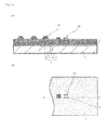
Figs. 14 (A) and (B) , the photosensitive resist 8 is removed from the thin-film multilayer body 7 using O2 plasma ashing. - In second and subsequent third processes, the above third process is repeated multiple times to process the thin-
film multilayer body 7 sequentially from its surface, thereby further forming thedevice section 10. In each of the repeated third processes, a photomask is positioned using an alignment mark formed in the previous third process. - First, the above third process is repeated using the
new alignment mark 31b to position a photomask (not illustrated), further forming thedevice section 10 and creating analignment mark 31c to be used in the next process on the thin-film multilayer body 7 as illustrated inFigs. 15 (A) and (B) . - Then the above third process is repeated using the
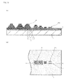
new alignment mark 31c to position a photomask (not illustrated), further forming thedevice section 10 and creating analignment mark 31d to be used in the next process on the thin-film multilayer body 7 as illustrated inFigs. 16 (A) and (B) . - Then the above third process is repeated using the
new alignment mark 31d to position a photomask (not illustrated), further forming thedevice section 10 and creating analignment mark 31e to be used in the next process on the thin-film multilayer body 7 as illustrated inFigs. 17 (A) and (B) . - In this way, during the processing of the thin-
film multilayer body 7, photomasks are positioned using an alignment mark formed in the previous process. This means that the photosensitive resist 8 is applied to and detached from the surface of the alignment mark only once before alignment, reducing damage to the alignment mark. Alignment using a less damaged alignment mark ensures a small misalignment between the correct position of the alignment mark and the recognized one, thereby helping to maintain the accuracy in the processing of thedevice section 10. - In a fourth process, the thin-
film multilayer device 100 is completed through the formation of an inorganicprotective film 12 made of SiO2 and an organicprotective film 13, which both surround thedevice section 10, and anouter electrode 14 connected to a portion of the conductivethin films 4 as capacitor electrodes. - First, the entire thin-
film multilayer body 7 including thedevice section 10 is subjected to a heat treatment at approximately 850°C. - Then as illustrated in
Figs. 18 (A) and (B) , an inorganicprotective film 12 made of SiO2 is formed using chemical vapor deposition (CVD). Then an organicprotective film 13 that functions as a positive photosensitive resist is applied using spin coating. The thickness of the inorganicprotective film 12 is, for example, 700 nm, and the thickness of the organicprotective film 13 is, for example, 5000 nm. - Then as illustrated in
Figs. 19 (A) and (B) , aphotomask 9f having analignment pattern 21f is placed in position on the organicprotective film 13 through, as in the second process, the alignment of acruciform alignment pattern 41e created in thephotomask 9f with thealignment mark 31e formed in the previous process. - Then the positive organic
protective film 13 is exposed through thephotomask 9f having thealignment pattern 21f and then developed to pattern the organicprotective film 13. - Then as illustrated in
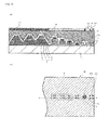
Figs. 20 (A) and (B) , the inorganicprotective film 12 and the dielectricthin films 5 are together dry-etched with CHF3 gas using the patterned organicprotective film 13 as a mask to expose a portion of the conductivethin films 4 as capacitor electrodes. Through this dry-etching of the inorganicprotective film 12, anew alignment mark 31f is also created. - Lastly, as illustrated in
Figs. 21 (A) and (B) , anouter electrode 14 is formed so as to be connected to a portion of the conducivethin films 4 as capacitor electrodes of thedevice section 10 through sputtering using thealignment mark 31f, completing the thin-film multilayer device 100. - More specifically, a Ti thin film, a Ni thin film, and a Au thin film are sequentially formed using sputtering. The thickness of the Ti thin film is, for example, 50 nm, the thickness of the Ni thin film is, for example, 1000 nm, and the thickness of the Au thin film is, for example, 200 nm.
- Then a positive photosensitive resist (not illustrated) is applied using spin coating.
- Then an alignment pattern created in a photomask (not illustrated) is aligned with the
alignment mark 31f, and this photomask is used to form a pattern corresponding to theouter electrode 14 in the photosensitive resist. Then the layer made up of the Ti thin film, the Ni thin film, and the Au thin film and masked with the photosensitive resist is processed using RIE, forming anouter electrode 14 connected to a portion of the conductivethin films 4 as capacitor electrodes. - Lastly, the photosensitive resist 8 is removed using O2 plasma ashing to complete a patterned
outer electrode 14. - Methods according to an embodiment of the present invention for producing a thin-film multilayer device are not limited to the above, and various modifications can be made without departing from the gist of the invention. For example, the third process, which is repeated multiple times in the production method according to the above embodiment, may be performed once. The photosensitive resists, which are positive ones in the above embodiment, may be negative ones. The number of layers etched together in each round of etching, which is one conductive thin film and one dielectric thin film in the above embodiment, is not limited. Furthermore, the alignment marks created in the thin-film multilayer body and the alignment pattern of the photomasks may have any shape that allows for accurate alignment for etching.
-
- 1
- Substrate
- 2
- Thermal oxide film
- 3, 5, 6
- Dielectric thin films
- 4
- Conductive thin film
- 7
- Thin-film multilayer body
- 8
- Photosensitive resist
- 8a
- Unexposed portion
- 8b
- Exposed portion
- 9a, 9b, 9f
- Photomasks
- 10
- Device section
- 11a, 11b, 11f
- Device-section patterns
- 12
- Inorganic protective film
- 13
- Organic protective film
- 14
- Outer electrode
- 21a, 21b, 21f, 41a, 41e
- Alignment patterns
- 31a to 31f
- Alignment marks
- 100
- Thin-film multilayer device
Claims (4)
- A method for producing a thin-film multilayer device, the method comprising
a first process having a step of forming a thin-film multilayer body having a plurality of thin films,
a second process having a step of applying a photosensitive resist to the thin-film multilayer body,
a step of exposing the resist through a photomask and developing the exposed resist,
a step of etching the thin-film multilayer body coated with the developed photosensitive resist to form a device section and an alignment mark on the thin-film multilayer body, and
a step of removing the photosensitive resist from the etched thin-film multilayer body, and
a third process having a step of applying a photosensitive resist to the thin-film multilayer body,
a step of placing a photomask having an alignment pattern in position on the photosensitive resist by aligning the alignment pattern with the alignment mark formed in the previous process,
a step of exposing the photosensitive resist through the photomask and developing the exposed photosensitive resist,
a step of etching the thin-film multilayer body coated with the developed photosensitive resist to form a device section and an alignment mark on the thin-film multilayer body, and
a step of removing the photosensitive resist from the etched thin-film multilayer body. - The method according to Claim 1 for producing a thin-film multilayer device, wherein the third process is repeated twice or more.
- The method according to Claim 1 or 2 for producing a thin-film multilayer device, wherein the alignment mark formed in a third process is created in a lower layer of the thin-film multilayer body than the alignment mark formed in the previous third process.
- The method according to any one of Claims 1 to 3 for producing a thin-film multilayer device, wherein the thin-film multilayer body includes an alternate stack of a conductive thin film and a dielectric thin film, and
in the second process or the third process, the conductive thin film and the dielectric thin film are etched together.
Applications Claiming Priority (2)
| Application Number | Priority Date | Filing Date | Title |
|---|---|---|---|
| JP2012144453 | 2012-06-27 | ||
| PCT/JP2013/066463 WO2014002794A1 (en) | 2012-06-27 | 2013-06-14 | Method for manufacturing thin film laminated element |
Publications (3)
| Publication Number | Publication Date |
|---|---|
| EP2869332A1 true EP2869332A1 (en) | 2015-05-06 |
| EP2869332A4 EP2869332A4 (en) | 2016-02-24 |
| EP2869332B1 EP2869332B1 (en) | 2017-03-15 |
Family
ID=49782956
Family Applications (1)
| Application Number | Title | Priority Date | Filing Date |
|---|---|---|---|
| EP13810224.9A Active EP2869332B1 (en) | 2012-06-27 | 2013-06-14 | Method for manufacturing thin film laminated element |
Country Status (5)
| Country | Link |
|---|---|
| EP (1) | EP2869332B1 (en) |
| JP (1) | JPWO2014002794A1 (en) |
| KR (1) | KR101708823B1 (en) |
| CN (1) | CN104471675B (en) |
| WO (1) | WO2014002794A1 (en) |
Cited By (1)
| Publication number | Priority date | Publication date | Assignee | Title |
|---|---|---|---|---|
| US11121092B2 (en) | 2019-06-27 | 2021-09-14 | Yangtze Memory Technologies Co., Ltd. | Marking pattern in forming staircase structure of three-dimensional memory device |
Families Citing this family (1)
| Publication number | Priority date | Publication date | Assignee | Title |
|---|---|---|---|---|
| JP7096200B2 (en) * | 2019-05-20 | 2022-07-05 | ユニ・チャーム株式会社 | How to make pet diapers, pet diaper enclosures and pet diapers |
Family Cites Families (10)
| Publication number | Priority date | Publication date | Assignee | Title |
|---|---|---|---|---|
| JPS594198A (en) * | 1982-06-30 | 1984-01-10 | 富士通株式会社 | Method of producing printed circuit board |
| JPH07202425A (en) * | 1993-12-28 | 1995-08-04 | Toray Ind Inc | Method for manufacturing multilayer wiring board |
| JP2001210571A (en) * | 2000-01-25 | 2001-08-03 | Daido Steel Co Ltd | Method of forming alignment mark |
| JP2002033458A (en) * | 2000-07-19 | 2002-01-31 | Nikon Corp | Semiconductor device and manufacturing method thereof |
| CN1480985A (en) * | 2002-09-04 | 2004-03-10 | 旺宏电子股份有限公司 | Method of peripheral auxiliary graphics for determining algnment mark of wafer and photoresist mask utilized |
| JP3972929B2 (en) * | 2004-09-27 | 2007-09-05 | セイコーエプソン株式会社 | Method for aligning exposure mask and method for manufacturing thin film element substrate |
| JP4029884B2 (en) * | 2005-03-29 | 2008-01-09 | セイコーエプソン株式会社 | Manufacturing method of semiconductor device |
| JP5163330B2 (en) * | 2008-07-14 | 2013-03-13 | 株式会社村田製作所 | Processing method of thin film laminate |
| TWI502623B (en) * | 2010-01-07 | 2015-10-01 | Hoya股份有限公司 | Photomask manufacturing method, photomask, and display device manufacturing method |
| JP2011238652A (en) * | 2010-05-06 | 2011-11-24 | Renesas Electronics Corp | Semiconductor device and method of manufacturing the same |
-
2013
- 2013-06-14 WO PCT/JP2013/066463 patent/WO2014002794A1/en not_active Ceased
- 2013-06-14 EP EP13810224.9A patent/EP2869332B1/en active Active
- 2013-06-14 JP JP2014522542A patent/JPWO2014002794A1/en active Pending
- 2013-06-14 KR KR1020147034558A patent/KR101708823B1/en active Active
- 2013-06-14 CN CN201380034371.5A patent/CN104471675B/en active Active
Cited By (4)
| Publication number | Priority date | Publication date | Assignee | Title |
|---|---|---|---|---|
| US11121092B2 (en) | 2019-06-27 | 2021-09-14 | Yangtze Memory Technologies Co., Ltd. | Marking pattern in forming staircase structure of three-dimensional memory device |
| US11545442B2 (en) | 2019-06-27 | 2023-01-03 | Yangtze Memory Technologies Co., Ltd. | Marking pattern in forming staircase structure of three-dimensional memory device |
| US11552025B2 (en) | 2019-06-27 | 2023-01-10 | Yangtze Memory Technologies Co., Ltd. | Marking pattern in forming staircase structure of three-dimensional memory device |
| US11594496B2 (en) | 2019-06-27 | 2023-02-28 | Yangtze Memory Technologies Co., Ltd. | Marking pattern in forming staircase structure of three-dimensional memory device |
Also Published As
| Publication number | Publication date |
|---|---|
| KR101708823B1 (en) | 2017-02-21 |
| JPWO2014002794A1 (en) | 2016-05-30 |
| EP2869332B1 (en) | 2017-03-15 |
| CN104471675B (en) | 2017-06-30 |
| EP2869332A4 (en) | 2016-02-24 |
| CN104471675A (en) | 2015-03-25 |
| KR20150013265A (en) | 2015-02-04 |
| WO2014002794A1 (en) | 2014-01-03 |
Similar Documents
| Publication | Publication Date | Title |
|---|---|---|
| KR101225601B1 (en) | Fabrication method of large area nanoscale pattern | |
| US10049878B2 (en) | Self-aligned patterning process | |
| US9892933B2 (en) | Lithography using multilayer spacer for reduced spacer footing | |
| US8941166B2 (en) | Multiple patterning method | |
| KR20110108780A (en) | Fine pattern manufacturing method | |
| EP2869332B1 (en) | Method for manufacturing thin film laminated element | |
| KR20150000040A (en) | Thin film transistor substrate and Method of manufacturing the same | |
| US9590231B2 (en) | Method of manufacturing 3D barrier substrate | |
| CN109917616B (en) | Manufacturing method of mask for double patterning and double patterning method | |
| CN106298507B (en) | patterning method | |
| US8930860B2 (en) | Layout decomposition method and method for manufacturing semiconductor device applying the same | |
| CN104425218A (en) | Double patterning process method for semiconductor structures | |
| CN104934302B (en) | The production method of semiconductor devices | |
| CN105826329A (en) | Manufacturing method of array substrate, array substrate and liquid crystal panel | |
| KR20080086685A (en) | Mask rework method | |
| US9032340B2 (en) | Layout decomposition method and method for manufacturing semiconductor device applying the same | |
| CN104950539B (en) | A kind of production method of display panel | |
| US10325778B2 (en) | Utilizing multiple layers to increase spatial frequency | |
| CN117751427B (en) | Method for manufacturing self-aligned quadruple patterned semiconductor device and semiconductor device | |
| US8728721B2 (en) | Methods of processing substrates | |
| JP2667517B2 (en) | Method of forming hole in interlayer insulating film | |
| CN112825315B (en) | Semiconductor structure and method of forming the same | |
| CN104425380A (en) | Forming method of grid of CMOS (Complementary Metal Oxide Semiconductor) inverter | |
| KR20100053897A (en) | Method for fabricating contact hole in semiconductor device | |
| JPH0472678A (en) | Manufacture of semiconductor device |
Legal Events
| Date | Code | Title | Description |
|---|---|---|---|
| PUAI | Public reference made under article 153(3) epc to a published international application that has entered the european phase |
Free format text: ORIGINAL CODE: 0009012 |
|
| 17P | Request for examination filed |
Effective date: 20141017 |
|
| AK | Designated contracting states |
Kind code of ref document: A1 Designated state(s): AL AT BE BG CH CY CZ DE DK EE ES FI FR GB GR HR HU IE IS IT LI LT LU LV MC MK MT NL NO PL PT RO RS SE SI SK SM TR |
|
| AX | Request for extension of the european patent |
Extension state: BA ME |
|
| DAX | Request for extension of the european patent (deleted) | ||
| RA4 | Supplementary search report drawn up and despatched (corrected) |
Effective date: 20160121 |
|
| RIC1 | Information provided on ipc code assigned before grant |
Ipc: H01L 49/02 20060101ALI20160115BHEP Ipc: H01L 23/544 20060101ALI20160115BHEP Ipc: H01L 27/01 20060101ALI20160115BHEP Ipc: H01L 21/60 20060101ALN20160115BHEP Ipc: H01G 4/12 20060101ALI20160115BHEP Ipc: H01L 21/02 20060101AFI20160115BHEP Ipc: G03F 9/00 20060101ALI20160115BHEP Ipc: H01G 4/33 20060101ALI20160115BHEP Ipc: H01L 21/311 20060101ALN20160115BHEP |
|
| REG | Reference to a national code |
Ref country code: DE Ref legal event code: R079 Ref document number: 602013018678 Country of ref document: DE Free format text: PREVIOUS MAIN CLASS: H01L0021027000 Ipc: H01L0023544000 |
|
| GRAP | Despatch of communication of intention to grant a patent |
Free format text: ORIGINAL CODE: EPIDOSNIGR1 |
|
| RIC1 | Information provided on ipc code assigned before grant |
Ipc: H01G 4/33 20060101ALI20160901BHEP Ipc: G03F 9/00 20060101ALI20160901BHEP Ipc: H01L 21/02 20060101ALI20160901BHEP Ipc: H01L 21/311 20060101ALN20160901BHEP Ipc: H01G 4/12 20060101ALI20160901BHEP Ipc: H01L 49/02 20060101ALI20160901BHEP Ipc: H01L 23/544 20060101AFI20160901BHEP |
|
| INTG | Intention to grant announced |
Effective date: 20160922 |
|
| GRAS | Grant fee paid |
Free format text: ORIGINAL CODE: EPIDOSNIGR3 |
|
| GRAA | (expected) grant |
Free format text: ORIGINAL CODE: 0009210 |
|
| AK | Designated contracting states |
Kind code of ref document: B1 Designated state(s): AL AT BE BG CH CY CZ DE DK EE ES FI FR GB GR HR HU IE IS IT LI LT LU LV MC MK MT NL NO PL PT RO RS SE SI SK SM TR |
|
| REG | Reference to a national code |
Ref country code: CH Ref legal event code: EP Ref country code: GB Ref legal event code: FG4D |
|
| REG | Reference to a national code |
Ref country code: IE Ref legal event code: FG4D |
|
| REG | Reference to a national code |
Ref country code: AT Ref legal event code: REF Ref document number: 876356 Country of ref document: AT Kind code of ref document: T Effective date: 20170415 |
|
| REG | Reference to a national code |
Ref country code: DE Ref legal event code: R096 Ref document number: 602013018678 Country of ref document: DE |
|
| REG | Reference to a national code |
Ref country code: NL Ref legal event code: MP Effective date: 20170315 |
|
| REG | Reference to a national code |
Ref country code: LT Ref legal event code: MG4D |
|
| PG25 | Lapsed in a contracting state [announced via postgrant information from national office to epo] |
Ref country code: HR Free format text: LAPSE BECAUSE OF FAILURE TO SUBMIT A TRANSLATION OF THE DESCRIPTION OR TO PAY THE FEE WITHIN THE PRESCRIBED TIME-LIMIT Effective date: 20170315 Ref country code: LT Free format text: LAPSE BECAUSE OF FAILURE TO SUBMIT A TRANSLATION OF THE DESCRIPTION OR TO PAY THE FEE WITHIN THE PRESCRIBED TIME-LIMIT Effective date: 20170315 Ref country code: FI Free format text: LAPSE BECAUSE OF FAILURE TO SUBMIT A TRANSLATION OF THE DESCRIPTION OR TO PAY THE FEE WITHIN THE PRESCRIBED TIME-LIMIT Effective date: 20170315 Ref country code: NO Free format text: LAPSE BECAUSE OF FAILURE TO SUBMIT A TRANSLATION OF THE DESCRIPTION OR TO PAY THE FEE WITHIN THE PRESCRIBED TIME-LIMIT Effective date: 20170615 Ref country code: GR Free format text: LAPSE BECAUSE OF FAILURE TO SUBMIT A TRANSLATION OF THE DESCRIPTION OR TO PAY THE FEE WITHIN THE PRESCRIBED TIME-LIMIT Effective date: 20170616 |
|
| REG | Reference to a national code |
Ref country code: AT Ref legal event code: MK05 Ref document number: 876356 Country of ref document: AT Kind code of ref document: T Effective date: 20170315 |
|
| PG25 | Lapsed in a contracting state [announced via postgrant information from national office to epo] |
Ref country code: RS Free format text: LAPSE BECAUSE OF FAILURE TO SUBMIT A TRANSLATION OF THE DESCRIPTION OR TO PAY THE FEE WITHIN THE PRESCRIBED TIME-LIMIT Effective date: 20170315 Ref country code: LV Free format text: LAPSE BECAUSE OF FAILURE TO SUBMIT A TRANSLATION OF THE DESCRIPTION OR TO PAY THE FEE WITHIN THE PRESCRIBED TIME-LIMIT Effective date: 20170315 Ref country code: SE Free format text: LAPSE BECAUSE OF FAILURE TO SUBMIT A TRANSLATION OF THE DESCRIPTION OR TO PAY THE FEE WITHIN THE PRESCRIBED TIME-LIMIT Effective date: 20170315 Ref country code: BG Free format text: LAPSE BECAUSE OF FAILURE TO SUBMIT A TRANSLATION OF THE DESCRIPTION OR TO PAY THE FEE WITHIN THE PRESCRIBED TIME-LIMIT Effective date: 20170615 |
|
| PG25 | Lapsed in a contracting state [announced via postgrant information from national office to epo] |
Ref country code: NL Free format text: LAPSE BECAUSE OF FAILURE TO SUBMIT A TRANSLATION OF THE DESCRIPTION OR TO PAY THE FEE WITHIN THE PRESCRIBED TIME-LIMIT Effective date: 20170315 |
|
| PG25 | Lapsed in a contracting state [announced via postgrant information from national office to epo] |
Ref country code: EE Free format text: LAPSE BECAUSE OF FAILURE TO SUBMIT A TRANSLATION OF THE DESCRIPTION OR TO PAY THE FEE WITHIN THE PRESCRIBED TIME-LIMIT Effective date: 20170315 Ref country code: SK Free format text: LAPSE BECAUSE OF FAILURE TO SUBMIT A TRANSLATION OF THE DESCRIPTION OR TO PAY THE FEE WITHIN THE PRESCRIBED TIME-LIMIT Effective date: 20170315 Ref country code: AT Free format text: LAPSE BECAUSE OF FAILURE TO SUBMIT A TRANSLATION OF THE DESCRIPTION OR TO PAY THE FEE WITHIN THE PRESCRIBED TIME-LIMIT Effective date: 20170315 Ref country code: IT Free format text: LAPSE BECAUSE OF FAILURE TO SUBMIT A TRANSLATION OF THE DESCRIPTION OR TO PAY THE FEE WITHIN THE PRESCRIBED TIME-LIMIT Effective date: 20170315 Ref country code: ES Free format text: LAPSE BECAUSE OF FAILURE TO SUBMIT A TRANSLATION OF THE DESCRIPTION OR TO PAY THE FEE WITHIN THE PRESCRIBED TIME-LIMIT Effective date: 20170315 Ref country code: RO Free format text: LAPSE BECAUSE OF FAILURE TO SUBMIT A TRANSLATION OF THE DESCRIPTION OR TO PAY THE FEE WITHIN THE PRESCRIBED TIME-LIMIT Effective date: 20170315 Ref country code: CZ Free format text: LAPSE BECAUSE OF FAILURE TO SUBMIT A TRANSLATION OF THE DESCRIPTION OR TO PAY THE FEE WITHIN THE PRESCRIBED TIME-LIMIT Effective date: 20170315 |
|
| PG25 | Lapsed in a contracting state [announced via postgrant information from national office to epo] |
Ref country code: PT Free format text: LAPSE BECAUSE OF FAILURE TO SUBMIT A TRANSLATION OF THE DESCRIPTION OR TO PAY THE FEE WITHIN THE PRESCRIBED TIME-LIMIT Effective date: 20170717 Ref country code: IS Free format text: LAPSE BECAUSE OF FAILURE TO SUBMIT A TRANSLATION OF THE DESCRIPTION OR TO PAY THE FEE WITHIN THE PRESCRIBED TIME-LIMIT Effective date: 20170715 Ref country code: PL Free format text: LAPSE BECAUSE OF FAILURE TO SUBMIT A TRANSLATION OF THE DESCRIPTION OR TO PAY THE FEE WITHIN THE PRESCRIBED TIME-LIMIT Effective date: 20170315 Ref country code: SM Free format text: LAPSE BECAUSE OF FAILURE TO SUBMIT A TRANSLATION OF THE DESCRIPTION OR TO PAY THE FEE WITHIN THE PRESCRIBED TIME-LIMIT Effective date: 20170315 |
|
| REG | Reference to a national code |
Ref country code: DE Ref legal event code: R097 Ref document number: 602013018678 Country of ref document: DE |
|
| PLBE | No opposition filed within time limit |
Free format text: ORIGINAL CODE: 0009261 |
|
| STAA | Information on the status of an ep patent application or granted ep patent |
Free format text: STATUS: NO OPPOSITION FILED WITHIN TIME LIMIT |
|
| PG25 | Lapsed in a contracting state [announced via postgrant information from national office to epo] |
Ref country code: MC Free format text: LAPSE BECAUSE OF FAILURE TO SUBMIT A TRANSLATION OF THE DESCRIPTION OR TO PAY THE FEE WITHIN THE PRESCRIBED TIME-LIMIT Effective date: 20170315 Ref country code: DK Free format text: LAPSE BECAUSE OF FAILURE TO SUBMIT A TRANSLATION OF THE DESCRIPTION OR TO PAY THE FEE WITHIN THE PRESCRIBED TIME-LIMIT Effective date: 20170315 |
|
| REG | Reference to a national code |
Ref country code: CH Ref legal event code: PL |
|
| 26N | No opposition filed |
Effective date: 20171218 |
|
| GBPC | Gb: european patent ceased through non-payment of renewal fee |
Effective date: 20170615 |
|
| PG25 | Lapsed in a contracting state [announced via postgrant information from national office to epo] |
Ref country code: SI Free format text: LAPSE BECAUSE OF FAILURE TO SUBMIT A TRANSLATION OF THE DESCRIPTION OR TO PAY THE FEE WITHIN THE PRESCRIBED TIME-LIMIT Effective date: 20170315 |
|
| REG | Reference to a national code |
Ref country code: IE Ref legal event code: MM4A |
|
| REG | Reference to a national code |
Ref country code: FR Ref legal event code: ST Effective date: 20180228 |
|
| PG25 | Lapsed in a contracting state [announced via postgrant information from national office to epo] |
Ref country code: IE Free format text: LAPSE BECAUSE OF NON-PAYMENT OF DUE FEES Effective date: 20170614 Ref country code: LU Free format text: LAPSE BECAUSE OF NON-PAYMENT OF DUE FEES Effective date: 20170614 Ref country code: CH Free format text: LAPSE BECAUSE OF NON-PAYMENT OF DUE FEES Effective date: 20170630 Ref country code: LI Free format text: LAPSE BECAUSE OF NON-PAYMENT OF DUE FEES Effective date: 20170630 Ref country code: GB Free format text: LAPSE BECAUSE OF NON-PAYMENT OF DUE FEES Effective date: 20170615 |
|
| PG25 | Lapsed in a contracting state [announced via postgrant information from national office to epo] |
Ref country code: FR Free format text: LAPSE BECAUSE OF NON-PAYMENT OF DUE FEES Effective date: 20170630 |
|
| REG | Reference to a national code |
Ref country code: BE Ref legal event code: MM Effective date: 20170630 |
|
| PG25 | Lapsed in a contracting state [announced via postgrant information from national office to epo] |
Ref country code: BE Free format text: LAPSE BECAUSE OF NON-PAYMENT OF DUE FEES Effective date: 20170630 |
|
| PG25 | Lapsed in a contracting state [announced via postgrant information from national office to epo] |
Ref country code: MT Free format text: LAPSE BECAUSE OF NON-PAYMENT OF DUE FEES Effective date: 20170614 |
|
| PG25 | Lapsed in a contracting state [announced via postgrant information from national office to epo] |
Ref country code: HU Free format text: LAPSE BECAUSE OF FAILURE TO SUBMIT A TRANSLATION OF THE DESCRIPTION OR TO PAY THE FEE WITHIN THE PRESCRIBED TIME-LIMIT; INVALID AB INITIO Effective date: 20130614 |
|
| PG25 | Lapsed in a contracting state [announced via postgrant information from national office to epo] |
Ref country code: CY Free format text: LAPSE BECAUSE OF FAILURE TO SUBMIT A TRANSLATION OF THE DESCRIPTION OR TO PAY THE FEE WITHIN THE PRESCRIBED TIME-LIMIT Effective date: 20170315 |
|
| PG25 | Lapsed in a contracting state [announced via postgrant information from national office to epo] |
Ref country code: MK Free format text: LAPSE BECAUSE OF FAILURE TO SUBMIT A TRANSLATION OF THE DESCRIPTION OR TO PAY THE FEE WITHIN THE PRESCRIBED TIME-LIMIT Effective date: 20170315 |
|
| PG25 | Lapsed in a contracting state [announced via postgrant information from national office to epo] |
Ref country code: TR Free format text: LAPSE BECAUSE OF FAILURE TO SUBMIT A TRANSLATION OF THE DESCRIPTION OR TO PAY THE FEE WITHIN THE PRESCRIBED TIME-LIMIT Effective date: 20170315 |
|
| PG25 | Lapsed in a contracting state [announced via postgrant information from national office to epo] |
Ref country code: AL Free format text: LAPSE BECAUSE OF FAILURE TO SUBMIT A TRANSLATION OF THE DESCRIPTION OR TO PAY THE FEE WITHIN THE PRESCRIBED TIME-LIMIT Effective date: 20170315 |
|
| PGFP | Annual fee paid to national office [announced via postgrant information from national office to epo] |
Ref country code: DE Payment date: 20250618 Year of fee payment: 13 |
|
| REG | Reference to a national code |
Ref country code: DE Ref legal event code: R079 Ref document number: 602013018678 Country of ref document: DE Free format text: PREVIOUS MAIN CLASS: H01L0023544000 Ipc: H10W0046000000 |