EP2869117A1 - Dual-viewing angle display panel and manufacturing method therefor - Google Patents
Dual-viewing angle display panel and manufacturing method therefor Download PDFInfo
- Publication number
- EP2869117A1 EP2869117A1 EP20120866988 EP12866988A EP2869117A1 EP 2869117 A1 EP2869117 A1 EP 2869117A1 EP 20120866988 EP20120866988 EP 20120866988 EP 12866988 A EP12866988 A EP 12866988A EP 2869117 A1 EP2869117 A1 EP 2869117A1
- Authority
- EP
- European Patent Office
- Prior art keywords
- transparent
- layer
- grating
- pixel
- viewing angle
- Prior art date
- Legal status (The legal status is an assumption and is not a legal conclusion. Google has not performed a legal analysis and makes no representation as to the accuracy of the status listed.)
- Ceased
Links
Images


Classifications
-
- G—PHYSICS
- G02—OPTICS
- G02B—OPTICAL ELEMENTS, SYSTEMS OR APPARATUS
- G02B30/00—Optical systems or apparatus for producing three-dimensional [3D] effects, e.g. stereoscopic images
- G02B30/20—Optical systems or apparatus for producing three-dimensional [3D] effects, e.g. stereoscopic images by providing first and second parallax images to an observer's left and right eyes
- G02B30/26—Optical systems or apparatus for producing three-dimensional [3D] effects, e.g. stereoscopic images by providing first and second parallax images to an observer's left and right eyes of the autostereoscopic type
- G02B30/30—Optical systems or apparatus for producing three-dimensional [3D] effects, e.g. stereoscopic images by providing first and second parallax images to an observer's left and right eyes of the autostereoscopic type involving parallax barriers
-
- G—PHYSICS
- G02—OPTICS
- G02F—OPTICAL DEVICES OR ARRANGEMENTS FOR THE CONTROL OF LIGHT BY MODIFICATION OF THE OPTICAL PROPERTIES OF THE MEDIA OF THE ELEMENTS INVOLVED THEREIN; NON-LINEAR OPTICS; FREQUENCY-CHANGING OF LIGHT; OPTICAL LOGIC ELEMENTS; OPTICAL ANALOGUE/DIGITAL CONVERTERS
- G02F1/00—Devices or arrangements for the control of the intensity, colour, phase, polarisation or direction of light arriving from an independent light source, e.g. switching, gating or modulating; Non-linear optics
- G02F1/01—Devices or arrangements for the control of the intensity, colour, phase, polarisation or direction of light arriving from an independent light source, e.g. switching, gating or modulating; Non-linear optics for the control of the intensity, phase, polarisation or colour
- G02F1/13—Devices or arrangements for the control of the intensity, colour, phase, polarisation or direction of light arriving from an independent light source, e.g. switching, gating or modulating; Non-linear optics for the control of the intensity, phase, polarisation or colour based on liquid crystals, e.g. single liquid crystal display cells
- G02F1/133—Constructional arrangements; Operation of liquid crystal cells; Circuit arrangements
- G02F1/1333—Constructional arrangements; Manufacturing methods
- G02F1/1335—Structural association of cells with optical devices, e.g. polarisers or reflectors
- G02F1/133509—Filters, e.g. light shielding masks
- G02F1/133512—Light shielding layers, e.g. black matrix
-
- G—PHYSICS
- G02—OPTICS
- G02F—OPTICAL DEVICES OR ARRANGEMENTS FOR THE CONTROL OF LIGHT BY MODIFICATION OF THE OPTICAL PROPERTIES OF THE MEDIA OF THE ELEMENTS INVOLVED THEREIN; NON-LINEAR OPTICS; FREQUENCY-CHANGING OF LIGHT; OPTICAL LOGIC ELEMENTS; OPTICAL ANALOGUE/DIGITAL CONVERTERS
- G02F1/00—Devices or arrangements for the control of the intensity, colour, phase, polarisation or direction of light arriving from an independent light source, e.g. switching, gating or modulating; Non-linear optics
- G02F1/01—Devices or arrangements for the control of the intensity, colour, phase, polarisation or direction of light arriving from an independent light source, e.g. switching, gating or modulating; Non-linear optics for the control of the intensity, phase, polarisation or colour
- G02F1/13—Devices or arrangements for the control of the intensity, colour, phase, polarisation or direction of light arriving from an independent light source, e.g. switching, gating or modulating; Non-linear optics for the control of the intensity, phase, polarisation or colour based on liquid crystals, e.g. single liquid crystal display cells
-
- G—PHYSICS
- G02—OPTICS
- G02B—OPTICAL ELEMENTS, SYSTEMS OR APPARATUS
- G02B30/00—Optical systems or apparatus for producing three-dimensional [3D] effects, e.g. stereoscopic images
- G02B30/20—Optical systems or apparatus for producing three-dimensional [3D] effects, e.g. stereoscopic images by providing first and second parallax images to an observer's left and right eyes
- G02B30/26—Optical systems or apparatus for producing three-dimensional [3D] effects, e.g. stereoscopic images by providing first and second parallax images to an observer's left and right eyes of the autostereoscopic type
- G02B30/27—Optical systems or apparatus for producing three-dimensional [3D] effects, e.g. stereoscopic images by providing first and second parallax images to an observer's left and right eyes of the autostereoscopic type involving lenticular arrays
-
- G—PHYSICS
- G02—OPTICS
- G02F—OPTICAL DEVICES OR ARRANGEMENTS FOR THE CONTROL OF LIGHT BY MODIFICATION OF THE OPTICAL PROPERTIES OF THE MEDIA OF THE ELEMENTS INVOLVED THEREIN; NON-LINEAR OPTICS; FREQUENCY-CHANGING OF LIGHT; OPTICAL LOGIC ELEMENTS; OPTICAL ANALOGUE/DIGITAL CONVERTERS
- G02F1/00—Devices or arrangements for the control of the intensity, colour, phase, polarisation or direction of light arriving from an independent light source, e.g. switching, gating or modulating; Non-linear optics
- G02F1/01—Devices or arrangements for the control of the intensity, colour, phase, polarisation or direction of light arriving from an independent light source, e.g. switching, gating or modulating; Non-linear optics for the control of the intensity, phase, polarisation or colour
- G02F1/13—Devices or arrangements for the control of the intensity, colour, phase, polarisation or direction of light arriving from an independent light source, e.g. switching, gating or modulating; Non-linear optics for the control of the intensity, phase, polarisation or colour based on liquid crystals, e.g. single liquid crystal display cells
- G02F1/133—Constructional arrangements; Operation of liquid crystal cells; Circuit arrangements
- G02F1/1333—Constructional arrangements; Manufacturing methods
-
- G—PHYSICS
- G09—EDUCATION; CRYPTOGRAPHY; DISPLAY; ADVERTISING; SEALS
- G09F—DISPLAYING; ADVERTISING; SIGNS; LABELS OR NAME-PLATES; SEALS
- G09F9/00—Indicating arrangements for variable information in which the information is built-up on a support by selection or combination of individual elements
-
- H—ELECTRICITY
- H04—ELECTRIC COMMUNICATION TECHNIQUE
- H04N—PICTORIAL COMMUNICATION, e.g. TELEVISION
- H04N13/00—Stereoscopic video systems; Multi-view video systems; Details thereof
- H04N13/30—Image reproducers
- H04N13/302—Image reproducers for viewing without the aid of special glasses, i.e. using autostereoscopic displays
- H04N13/305—Image reproducers for viewing without the aid of special glasses, i.e. using autostereoscopic displays using lenticular lenses, e.g. arrangements of cylindrical lenses
-
- Y—GENERAL TAGGING OF NEW TECHNOLOGICAL DEVELOPMENTS; GENERAL TAGGING OF CROSS-SECTIONAL TECHNOLOGIES SPANNING OVER SEVERAL SECTIONS OF THE IPC; TECHNICAL SUBJECTS COVERED BY FORMER USPC CROSS-REFERENCE ART COLLECTIONS [XRACs] AND DIGESTS
- Y10—TECHNICAL SUBJECTS COVERED BY FORMER USPC
- Y10T—TECHNICAL SUBJECTS COVERED BY FORMER US CLASSIFICATION
- Y10T156/00—Adhesive bonding and miscellaneous chemical manufacture
- Y10T156/10—Methods of surface bonding and/or assembly therefor
Definitions
- Embodiments of the invention relate to a two-way viewing angle display panel and its fabrication method.
- a two-way (also known as two-way video) viewing angle display different images are displayed at different angles, that is to say, users may see different images on the display from different angels.
- the two-way display may be applied to in-vehicle display.
- passengers at different seats in the car may see different images on the same display. Therefore, it is not necessary to provide individual displays for each passenger, which will reduce costs of display arrangement and usage of in-vehicle space.
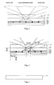
- a conventional two-way viewing angle display comprises: a first substrate 11, a liquid crystal layer 12, a pixel layer 13, a second substrate 14, a patterned-shield layer 15 and a transparent substrate 16, where the patterned-shield layer 15 comprises opaque light-shield layer patterns 151, 152, 153 and 154.
- the patterned-shield layer 15 comprises opaque light-shield layer patterns 151, 152, 153 and 154.
- the patterned-shield layer 15 is attached to the second substrate 14. Therefore, the distance between the pixel layer 13 and the patterned-shield layer 15 is long, which narrows the two-way viewing angles and negatively affect the user experience.
- a thickness of the second substrate 14 is reduced to optimize the two-way viewable angles.
- reduction in the thickness of the second substrate 14 will produce various problems during manufacture, such as decrease in flatness of the substrate, breaking of the substrate, failure in liquid crystal filling and the like, and thus significantly reduces the yield rate (i.e. fine goods rate) of the products.
- Embodiments of the invention provide the following technical solutions.
- an embodiment of the invention provides a method for fabricating a two-way viewing angle display panel, which comprises:
- the step of forming a grating made of a light-shield layer on the transparent substrate comprises:
- the light-shield layer is a black metal layer, or an organic material layer, or a laminated layer made of an organic material and a reflective material.
- the step of forming a transparent adjusting layer on the transparent substrate having the grating formed thereon comprises:
- a thickness of the transparent adjusting layer is 0-500 ⁇ m.
- the method further comprises the following steps before forming the transparent adjusting layer on the transparent substrate having the grating formed thereon:
- the thickness of the second substrate is reduced to optimize the two-way viewing angles.
- reduction in the thickness of the second substrate will produce various problems during manufacture, such as decrease in flatness of the substrate, breaking of the substrate, failure in liquid crystal filling and the like, and thus significantly reduce the yield rate of the products.
- embodiments of the invention provide a two-way viewing angle display panel and its fabrication method which may optimize the two-way viewing angles and avoid the yield rate issue caused by reducing the thickness of the substrate.
- An embodiment of the invention provides a method for fabricating a two-way viewing angle display panel, the method comprises:
- the grating made of the light-shield layer is formed on the transparent substrate, followed by forming the transparent adjusting layer on the transparent substrate having the grating, and then forming the pixel layer on the transparent adjusting layer.
- the grating of the two-way viewing angle display panel is positioned on the inner side of the substrate and is separated from the pixel layer by the transparent adjusting layer. Therefore, the distance between the grating and the pixel layer may be adjusted by adjusting the thickness of the transparent adjusting layer, thereby optimizing the two-way view angle. Moreover, it is not needed to reduce the thickness of the substrate, thereby avoiding the yield rate problem cause by thinned substrate.
- a two-way viewing angle display panel as illustrated in Fig.2 which comprises:
- the grating is positioned on the inner side of the substrate and is separated from the pixel layer by the transparent adjusting layer. Therefore, the distance between the grating and the pixel layer may be adjusted by adjusting the thickness of the transparent adjusting layer, thereby optimizing the two-way viewing angle. Moreover, it is not needed to reduce the thickness of the substrate, thereby avoiding the yield rate problem cause by thinned substrate.
- Fig. 3 schematically illustrates a visual area of a two-way viewing angle display panel in accordance with an embodiment of the invention.
- light from a backlight source 21 pass through the grating 18 to form a left visual area and a right visual area, as well as a cross-interference area in which both the left and right images may be seen.
- the cross-interference area will be narrowed accordingly, if the left and right visual areas may be enlarged to their most.
- Fig. 4 schematically illustrates visual angles of a two-way viewing angle display panel in accordance with an embodiment of the invention.
- the left and right visual angles of the two-way viewing angle display panel are symmetrical and a central axis of a grating aperture at the symmetrical center of the grating is aligned with a black matrix on a vertical central axis of the pixel layer 13, thereby ensuring the symmetry of the left and right visual angles.
- the aperture size of the grating is a
- the distance between the grating and the pixel layer, that is, the thickness of the transparent adjusting layer, is h
- the refractive index of the transparent substrate is n
- the transparent substrate is made of glass or an organic material having a refractive index n of 1 ⁇ 1.5.
- the central-interference angle will be decreased when the grating aperture a is reduced and the width m of the black matrix is increased, while the central-interference angle will be increased when h is reduced.
- the positioning height of the grating (that is, the thickness of the transparent adjusting layer) should be as close as possible to Ps/4 when fabricating a given two-way viewing angle display panel.
- Step 1 as illustrated in Fig. 5 , a transparent substrate 17 is provided, which is cleaned before the fabrication.
- a material of the transparent substrate 17 may be glass or an organic material.
- Step 2 as illustrated in Fig. 6 , a mask is used to form a grating 18 made of a light-shield layer on the transparent substrate 17.
- the mask includes not only a pattern for making the grating but also process marks needed for making the display panel, such as a polyimide (PI) mark, a seal mark, a cutting mark, an alignment mark for the mask and a mask carrier as well as a glass platform, and an alignment mark for the black matrices and color filter elements for forming the pixel layer.
- PI polyimide
- the process marks needed for fabricating the display panel are formed at the same time with the pixel layer.
- the process marks may affect the display of the grating aperture area.
- the process marks are formed at the same time when the grating is formed.
- the light-shield layer is made of an opaque material, for example, it may be a black metal layer made of chromium (Cr).
- the light-shield layer is made of the same organic material as the black matrix.
- the light-shield layer may be a laminated layer of an organic material layer and a reflector layer, where the reflector layer may reflect light to improve the transmittance and usage of the light, thereby improving the display brightness of the two-way viewing angle display panel.
- the reflector layer may be made of aluminum (Al), for example.
- Step 3 as illustrated in Fig. 7 , a transparent adjusting layer 19 may be formed on the transparent substrate 17 having the grating 18 formed thereon by blade coating or spin coating.
- the transparent adjusting layer 19 may adjust the distance between the grating 18 and the pixel layer 13.
- the thickness of the transparent adjusting layer 19 may be for example 0-500 ⁇ m. Specifically, the thickness of the transparent adjusting layer 19 may be determined by the design in accordance with the embodiments of the invention described above.
- a material of the transparent adjusting layer may be an insulating material or a metal material. When the grating 18 is made of an insulating material, the transparent adjusting layer 19 may use a metal material, thereby providing a better flatness for the transparent adjusting layer 19.
- Step 4 as illustrated in Fig. 8 , forming black matrices (BM) and color filter elements (RGB) for the pixel layer 13 on the transparent adjusting layer 19 using conventional processes.
- BM black matrices
- RGB color filter elements
- Step 5 as illustrated in Fig. 9 , forming a transparent conductive layer 20 on the pixel layer 13, where the transparent conductive layer 20 may be made of ITO.
- Step 6 as illustrated in Fig. 10 , a lower substrate 22 and the substrate 17 having the grating 18, the transparent adjusting layer 19, the pixel layer 13 and the transparent conductive layer 20 formed thereon are assembled using conventional PI rubbing to form a cell and the liquid crystal is filled to form the two-way viewing angle display panel as illustrated in Fig. 10 .
- the grating of the two-way viewing angle display panel is positioned on the inner side of the substrate and is separated from the pixel layer by the transparent adjusting layer.
- the thickness of the transparent adjusting layer may be adjusted according to the designed parameters of a given display panel, thereby optimizing the two-way view angle. Moreover, it is not needed to reduce the thickness of the substrate, thereby avoiding the yield rate problem caused by thinned substrate.
Landscapes
- Physics & Mathematics (AREA)
- Nonlinear Science (AREA)
- General Physics & Mathematics (AREA)
- Optics & Photonics (AREA)
- Chemical & Material Sciences (AREA)
- Crystallography & Structural Chemistry (AREA)
- Engineering & Computer Science (AREA)
- Mathematical Physics (AREA)
- Multimedia (AREA)
- Signal Processing (AREA)
- Theoretical Computer Science (AREA)
- Devices For Indicating Variable Information By Combining Individual Elements (AREA)
- Liquid Crystal (AREA)
- Optical Filters (AREA)
- Electroluminescent Light Sources (AREA)
Abstract
Description
- Embodiments of the invention relate to a two-way viewing angle display panel and its fabrication method.
- In a two-way (also known as two-way video) viewing angle display, different images are displayed at different angles, that is to say, users may see different images on the display from different angels. As an example, the two-way display may be applied to in-vehicle display. With a two-way viewing angle display, passengers at different seats in the car may see different images on the same display. Therefore, it is not necessary to provide individual displays for each passenger, which will reduce costs of display arrangement and usage of in-vehicle space.
- As illustrated in
Fig. 1 , a conventional two-way viewing angle display comprises: afirst substrate 11, aliquid crystal layer 12, apixel layer 13, asecond substrate 14, a patterned-shield layer 15 and atransparent substrate 16, where the patterned-shield layer 15 comprises opaque light-shield layer patterns shield layer 15 of the two-way view angle display. - In the two-way viewing angle display configured as above, the patterned-
shield layer 15 is attached to thesecond substrate 14. Therefore, the distance between thepixel layer 13 and the patterned-shield layer 15 is long, which narrows the two-way viewing angles and negatively affect the user experience. To increase the two-way viewable angles, in conventional technologies usually a thickness of thesecond substrate 14 is reduced to optimize the two-way viewable angles. However, reduction in the thickness of thesecond substrate 14 will produce various problems during manufacture, such as decrease in flatness of the substrate, breaking of the substrate, failure in liquid crystal filling and the like, and thus significantly reduces the yield rate (i.e. fine goods rate) of the products. - Embodiments of the invention provide the following technical solutions.
- In one aspect, an embodiment of the invention provides a method for fabricating a two-way viewing angle display panel, which comprises:
- providing a transparent substrate;
- forming a grating made of a light-shield layer on the transparent substrate;
- forming a transparent adjusting layer on the transparent substrate having the grating formed thereon; and
- sequentially forming a pixel layer and a transparent conductive layer on the transparent adjusting layer.
- Furthermore, the step of forming a grating made of a light-shield layer on the transparent substrate comprises:
- forming alignment marks for the grating and the pixel layer on the substrate at the same time by using the same mask plate.
- Furthermore, the light-shield layer is a black metal layer, or an organic material layer, or a laminated layer made of an organic material and a reflective material.
- Furthermore, the step of forming a transparent adjusting layer on the transparent substrate having the grating formed thereon comprises:
- blade or spin coating a transparent material on the transparent substrate having the grating formed thereon and then thermally curing the transparent material to form the transparent adjusting layer; or
- blade or spin coating a transparent material on the transparent substrate having the grating formed thereon and then UV curing the transparent material to form the transparent adjusting layer; or
- blade or spin coating a transparent material on the transparent substrate having the grating formed thereon and then UV pre-curing, followed by thermally curing the transparent material, to form the transparent adjusting layer; or
- depositing a non-metal transparent material on the transparent substrate having the grating formed thereon using CVD process to form the transparent adjusting layer; or
- depositing a transparent metal material on the transparent substrate having the grating formed thereon using sputtering process to form the transparent adjusting layer.
- Furthermore, a thickness of the transparent adjusting layer is 0-500µm.
- Furthermore, the method further comprises the following steps before forming the transparent adjusting layer on the transparent substrate having the grating formed thereon:
- obtaining a width of a sub-pixel of the pixel layer and a aperture size of the grating;
- determining the thickness of the transparent adjusting layer according to the width of the sub-pixel and the aperture size.
- Furthermore, a distance between the grating and the pixel layer, that is, the thickness h of the transparent adjusting layer, is determined according to the following equation:

where each sub-pixel of the pixel layer is made of a color filter element and a black matrix, the black matrix has a width of m, the color filter element has a width of p, each sub-pixel has a width of Ps=p+m, and the aperture size of the grating is a.
furthermore, h=Ps/4. - Another embodiment of the invention further provides a two-way viewing angle display panel comprising:
- a transparent substrate;
- a grating made of a light-shield layer on the transparent substrate;
- a transparent adjusting layer on the transparent substrate having the grating formed thereon; and
- a pixel layer and a transparent conductive layer on the transparent adjusting layer.
- Furthermore, a distance between the grating and the pixel layer, that is, a thickness of the transparent adjusting layer, is:

where each sub-pixel of the pixel layer is made of a color filter element and a black matrix, the black matrix has a width of m, the color filter element has a width of p, each sub-pixel has a width of Ps=p+m, and the aperture size of the grating is a. - In order to clearly illustrate the technical solutions of the embodiments of the invention, the drawings of the embodiments will be briefly described in the following; it is obvious that the described drawings are only related to some embodiments of the invention and thus are not limitative of the invention.
-
Fig. 1 schematically illustrates a configuration of a conventional two-way viewing angle display; -
Fig. 2 schematically illustrates a configuration of a two-way viewing angle display panel in accordance with an embodiment of the invention; -
Fig. 3 schematically illustrates a visual area of a two-way viewing angle display panel in accordance with an embodiment of the invention; -
Fig. 4 schematically illustrates visual angles of a two-way viewing angle display panel in accordance with an embodiment of the invention; -
Figs. 5 to 10 illustrate a process of a method for fabricating a two-way viewing angle display panel in accordance with an embodiment of the invention. - In order to make objects, technical details and advantages of the embodiments of the invention apparent, the technical solutions of the embodiment will be described in a clearly and fully understandable way in connection with the drawings related to the embodiments of the invention. It is obvious that the described embodiments are just a part but not all of the embodiments of the invention. Based on the described embodiments herein, those skilled in the art can obtain other embodiment(s), without any inventive work, which should be within the scope of the invention.
- According to conventional technologies, the thickness of the second substrate is reduced to optimize the two-way viewing angles. However, reduction in the thickness of the second substrate will produce various problems during manufacture, such as decrease in flatness of the substrate, breaking of the substrate, failure in liquid crystal filling and the like, and thus significantly reduce the yield rate of the products. To address the above problems, embodiments of the invention provide a two-way viewing angle display panel and its fabrication method which may optimize the two-way viewing angles and avoid the yield rate issue caused by reducing the thickness of the substrate.
- An embodiment of the invention provides a method for fabricating a two-way viewing angle display panel, the method comprises:
- Providing a
transparent substrate 17; - Forming a
grating 18 made of a light-shield layer on thetransparent substrate 17; - Forming a
transparent adjusting layer 19 on thetransparent substrate 17 having thegrating 18 formed thereon; - Sequentially forming a
pixel layer 13 and a transparentconductive layer 20 on thetransparent adjusting layer 19. - According to the embodiment of the method for fabricating the two-way viewing angle display panel of the invention, the grating made of the light-shield layer is formed on the transparent substrate, followed by forming the transparent adjusting layer on the transparent substrate having the grating, and then forming the pixel layer on the transparent adjusting layer. In the technical solution of the invention, the grating of the two-way viewing angle display panel is positioned on the inner side of the substrate and is separated from the pixel layer by the transparent adjusting layer. Therefore, the distance between the grating and the pixel layer may be adjusted by adjusting the thickness of the transparent adjusting layer, thereby optimizing the two-way view angle. Moreover, it is not needed to reduce the thickness of the substrate, thereby avoiding the yield rate problem cause by thinned substrate.
- After the completion of the above described steps, a two-way viewing angle display panel as illustrated in
Fig.2 is obtained, which comprises: - a
transparent substrate 17, - a grating 18 made of a light-shield layer on the
transparent substrate 17; - a
transparent adjusting layer 19 on thetransparent substrate 17 having the grating 18 formed thereon; - a
pixel layer 13 and a transparentconductive layer 20 on thetransparent adjusting layer 19. - In the two-way viewing angle display panel according to the embodiment of the invention, the grating is positioned on the inner side of the substrate and is separated from the pixel layer by the transparent adjusting layer. Therefore, the distance between the grating and the pixel layer may be adjusted by adjusting the thickness of the transparent adjusting layer, thereby optimizing the two-way viewing angle. Moreover, it is not needed to reduce the thickness of the substrate, thereby avoiding the yield rate problem cause by thinned substrate.
-
Fig. 3 schematically illustrates a visual area of a two-way viewing angle display panel in accordance with an embodiment of the invention. As shown inFig. 3 , light from abacklight source 21 pass through the grating 18 to form a left visual area and a right visual area, as well as a cross-interference area in which both the left and right images may be seen. The cross-interference area will be narrowed accordingly, if the left and right visual areas may be enlarged to their most. - In the configuration, the size of the visual area is related to the size of apertures and positioning height of the grating. Accordingly, an embodiment of the invention proposes a solution for designing a configuration of the two-way viewing angle display panel such that the visual area is maximized.
Fig. 4 schematically illustrates visual angles of a two-way viewing angle display panel in accordance with an embodiment of the invention. As shown inFig. 4 , the left and right visual angles of the two-way viewing angle display panel are symmetrical and a central axis of a grating aperture at the symmetrical center of the grating is aligned with a black matrix on a vertical central axis of thepixel layer 13, thereby ensuring the symmetry of the left and right visual angles. - As shown in
Fig. 4 , each sub-pixel of the pixel layer comprises a color filter element having a width of p and a black matrix having a width of m, thus, a width Ps of the sub-pixel is Ps=p+m. Moreover, the aperture size of the grating is a, the distance between the grating and the pixel layer, that is, the thickness of the transparent adjusting layer, is h, the refractive index of the transparent substrate is n and an actual visual angle of the two-way viewing angle display is (α1+β1). It is known from the refraction law that:

- Moreover,


- From which it is deduced that:


- Where the transparent substrate is made of glass or an organic material having a refractive index n of 1∼1.5. For simplicity, it is assumed that n is 1, thus:

- For the function

- it is easily known according to knowledge of functions that f(h) has a minimum value and sin(α1-β1) has a maximum value when (a-m)(3m+2p-a)=(2h)2. In that case the following may be deduced:

- While the distance Ps between two sub-pixels is Ps=p+m, therefore,

- Here

- Therefore, it is known from equation (10) that for a given display panel with a constant value Ps, the visual angles may be increased by appropriately increasing the width m of the black matrix and reducing the aperture size a.
- It is seen from equations (8) and (11) that when the positional height h of the grating is

- Moreover, the central-interference angle is 2(90° -α1), and

- Thus, the central-interference angle will be decreased when the grating aperture a is reduced and the width m of the black matrix is increased, while the central-interference angle will be increased when h is reduced.
- However, the following holds for h:

- In summary, a relatively large visual angle and a relatively small central-interference angle may be obtained when h=Ps/4. Thus, the positioning height of the grating (that is, the thickness of the transparent adjusting layer) should be as close as possible to Ps/4 when fabricating a given two-way viewing angle display panel.
- In the following, a method for fabricating the two-way viewing angle display panel in accordance with an embodiment of the invention will be described in detail in connection with
Figs. 5 to 10 . - Step 1: as illustrated in
Fig. 5 , atransparent substrate 17 is provided, which is cleaned before the fabrication. A material of thetransparent substrate 17 may be glass or an organic material. - Step 2: as illustrated in
Fig. 6 , a mask is used to form a grating 18 made of a light-shield layer on thetransparent substrate 17. Please note that the mask includes not only a pattern for making the grating but also process marks needed for making the display panel, such as a polyimide (PI) mark, a seal mark, a cutting mark, an alignment mark for the mask and a mask carrier as well as a glass platform, and an alignment mark for the black matrices and color filter elements for forming the pixel layer. - Conventionally, the process marks needed for fabricating the display panel are formed at the same time with the pixel layer. In the embodiment of the invention, if the process marks needed for fabricating the display panel are formed at the same time of forming the pixel layer, the process marks may affect the display of the grating aperture area. Thus, in the embodiment, the process marks are formed at the same time when the grating is formed.
- In the above configuration, the light-shield layer is made of an opaque material, for example, it may be a black metal layer made of chromium (Cr). Alternatively, the light-shield layer is made of the same organic material as the black matrix. Furthermore, the light-shield layer may be a laminated layer of an organic material layer and a reflector layer, where the reflector layer may reflect light to improve the transmittance and usage of the light, thereby improving the display brightness of the two-way viewing angle display panel. Here, the reflector layer may be made of aluminum (Al), for example.
- Step 3: as illustrated in
Fig. 7 , atransparent adjusting layer 19 may be formed on thetransparent substrate 17 having the grating 18 formed thereon by blade coating or spin coating. - The ways in which the
transparent adjusting layer 19 may be formed are listed as below: - a transparent material is blade or spin coated on the
transparent substrate 17 having the grating 18 formed thereon, and then thermally cured to form thetransparent adjusting layer 19; or - a transparent material is blade or spin coated on the
transparent substrate 17 having the grating 18 formed thereon, and then UV cured to form thetransparent adjusting layer 19; or - a transparent material is blade or spin coated on the
transparent substrate 17 having the grating 18 formed thereon and then UV pre-cured and followed by thermal cure to form thetransparent adjusting layer 19; or - a non-metal transparent material is deposited on the
transparent substrate 17 having the grating 18 formed thereon using CVD to form thetransparent adjusting layer 19; or - a transparent metal material is sputtered on the
transparent substrate 17 having the grating 18 formed thereon to form thetransparent adjusting layer 19. - The
transparent adjusting layer 19 may adjust the distance between the grating 18 and thepixel layer 13. The thickness of thetransparent adjusting layer 19 may be for example 0-500µm. Specifically, the thickness of thetransparent adjusting layer 19 may be determined by the design in accordance with the embodiments of the invention described above. A material of the transparent adjusting layer may be an insulating material or a metal material. When the grating 18 is made of an insulating material, thetransparent adjusting layer 19 may use a metal material, thereby providing a better flatness for thetransparent adjusting layer 19. - Step 4: as illustrated in
Fig. 8 , forming black matrices (BM) and color filter elements (RGB) for thepixel layer 13 on thetransparent adjusting layer 19 using conventional processes. Please note, for the mask used for forming the black matrices, the peripheral process marks thereon may be omitted while the alignment marks for the black matrix and the grating must be retained, and it should be ensured that the locations of such alignment marks do not influence the alignment marks for the RGB layer and the grating. - Step 5: as illustrated in
Fig. 9 , forming a transparentconductive layer 20 on thepixel layer 13, where the transparentconductive layer 20 may be made of ITO. - Step 6: as illustrated in
Fig. 10 , alower substrate 22 and thesubstrate 17 having the grating 18, thetransparent adjusting layer 19, thepixel layer 13 and the transparentconductive layer 20 formed thereon are assembled using conventional PI rubbing to form a cell and the liquid crystal is filled to form the two-way viewing angle display panel as illustrated inFig. 10 . - According to embodiment of the method for fabricating the two-way viewing angle display panel, the grating of the two-way viewing angle display panel is positioned on the inner side of the substrate and is separated from the pixel layer by the transparent adjusting layer. The thickness of the transparent adjusting layer may be adjusted according to the designed parameters of a given display panel, thereby optimizing the two-way view angle. Moreover, it is not needed to reduce the thickness of the substrate, thereby avoiding the yield rate problem caused by thinned substrate.
- In the method embodiments of the invention, the sequential number of each step is not used to limit the order of the steps. Instead, the order of the steps may be changed by those skilled in the art without any inventive effort and is thus under the protection of the invention.
- What are described above is related to the illustrative embodiments of the disclosure only and not limitative to the scope of the disclosure; the scopes of the disclosure are defined by the accompanying claims.
Claims (10)
- A method for fabricating a two-way viewing angle display panel, comprising:providing a transparent substrate;forming a grating made of a light-shield layer on the transparent substrate;forming a transparent adjusting layer on the transparent substrate having the grating formed thereon; andsequentially forming a pixel layer and a transparent conductive layer on the transparent adjusting layer.
- The method for fabricating a two-way viewing angle display panel of claim 1, wherein the step of forming a grating made of a light-shield layer on the transparent substrate comprises:forming alignment marks for the grating and the pixel layer on the substrate at the same time by using the same mask plate.
- The method for fabricating a two-way viewing angle display panel of claim 1 or 2, wherein the light-shield layer is a black metal layer, or an organic material layer, or a laminated layer made of an organic material and a reflective material.
- The method for fabricating a two-way viewing angle display panel of any of claims 1 to 3, wherein the step of forming a transparent adjusting layer on the transparent substrate having the grating formed thereon comprises:blade or spin coating a transparent material on the transparent substrate having the grating formed thereon and then thermally curing the transparent material to form the transparent adjusting layer; orblade or spin coating a transparent material on the transparent substrate having the grating formed thereon and then UV curing the transparent material to form the transparent adjusting layer; orblade or spin coating a transparent material on the transparent substrate having the grating formed thereon and then UV pre-curing, followed by thermally curing the transparent material to form the transparent adjusting layer; ordepositing a non-metal transparent material on the transparent substrate having the grating formed thereon using CVD process to form the transparent adjusting layer; ordepositing a transparent metal material on the transparent substrate having the grating formed thereon using sputtering process to form the transparent adjusting layer.
- The method for fabricating a two-way viewing angle display panel of any of claims 1 to 4, wherein a thickness of the transparent adjusting layer is 0-500µm.
- The method for fabricating a two-way viewing angle display panel of any of claims 1 to 5, further comprises the following steps before forming the transparent adjusting layer on the transparent substrate having the grating formed thereon:obtaining a width of a sub-pixel of the pixel layer and a aperture size of the grating;determining the thickness of the transparent adjusting layer according to the width of a sub-pixel and the aperture size.
- The method for fabricating a two-way viewing angle display panel of any of claims 1 to 6, wherein a distance between the grating and the pixel layer, that is, the thickness h of the transparent adjusting layer, is determined according to the following equation:

where each sub-pixel of the pixel layer is made of a color filter element and a black matrix, the black matrix has a width of m, the color filter element has a width of p, each sub-pixel has a width of Ps=p+m, and the aperture size of the grating is a. - The method for fabricating a two-way viewing angle display panel of claim 7, wherein h=Ps/4.
- A two-way viewing angle display panel comprising:a transparent substrate;a grating made of a light-shield layer on the transparent substrate;a transparent adjusting layer on the transparent substrate having the grating formed thereon; anda pixel layer and a transparent conductive layer on the transparent adjusting layer.
- The two-way viewing angle display panel of claim 9, wherein a distance between the grating and the pixel layer, that is, a thickness of the transparent adjusting layer, is:

where each sub-pixel of the pixel layer is made of a color filter element and a black matrix, the black matrix has a width of m, the color filter element has a width of p, each sub-pixel has a width of Ps=p+m, and the aperture size of the grating is a.
Applications Claiming Priority (2)
| Application Number | Priority Date | Filing Date | Title |
|---|---|---|---|
| CN201210228457.9A CN102768424B (en) | 2012-07-02 | 2012-07-02 | Double-viewing angle display panel and manufacturing method thereof |
| PCT/CN2012/087227 WO2014005412A1 (en) | 2012-07-02 | 2012-12-23 | Dual-viewing angle display panel and manufacturing method therefor |
Publications (2)
| Publication Number | Publication Date |
|---|---|
| EP2869117A1 true EP2869117A1 (en) | 2015-05-06 |
| EP2869117A4 EP2869117A4 (en) | 2016-03-16 |
Family
ID=47095874
Family Applications (1)
| Application Number | Title | Priority Date | Filing Date |
|---|---|---|---|
| EP12866988.4A Ceased EP2869117A4 (en) | 2012-07-02 | 2012-12-23 | DOUBLE VISUAL ANGLE DISPLAY PANEL AND METHOD FOR MANUFACTURING THE SAME |
Country Status (6)
| Country | Link |
|---|---|
| US (1) | US9304352B2 (en) |
| EP (1) | EP2869117A4 (en) |
| JP (1) | JP6143857B2 (en) |
| KR (1) | KR101545421B1 (en) |
| CN (1) | CN102768424B (en) |
| WO (1) | WO2014005412A1 (en) |
Families Citing this family (12)
| Publication number | Priority date | Publication date | Assignee | Title |
|---|---|---|---|---|
| CN102768424B (en) | 2012-07-02 | 2014-07-09 | 京东方科技集团股份有限公司 | Double-viewing angle display panel and manufacturing method thereof |
| CN102981306B (en) * | 2012-12-07 | 2016-03-30 | 京东方科技集团股份有限公司 | A kind of method for making of colored filter |
| CN103268033B (en) * | 2013-05-16 | 2016-03-30 | 京东方科技集团股份有限公司 | A kind of Double-vision touch display device and preparation method thereof |
| CN104111560B (en) | 2014-07-09 | 2017-08-29 | 京东方科技集团股份有限公司 | A kind of liquid crystal panel and double vision liquid crystal display device |
| CN104460100B (en) | 2014-11-26 | 2018-03-27 | 京东方科技集团股份有限公司 | Display base plate and display panel and preparation method thereof, display device |
| CN104656307B (en) * | 2015-03-25 | 2017-12-08 | 京东方科技集团股份有限公司 | Double-view field display panel and dual field of view display device |
| CN104730604A (en) * | 2015-04-21 | 2015-06-24 | 合肥京东方光电科技有限公司 | Light refraction structure and manufacturing method thereof, color film substrate and manufacturing method thereof and display device |
| WO2016180048A1 (en) * | 2015-05-13 | 2016-11-17 | 京东方科技集团股份有限公司 | Display device and drive method therefor |
| WO2017195323A1 (en) * | 2016-05-12 | 2017-11-16 | シャープ株式会社 | Liquid crystal display device |
| CN107219671A (en) * | 2017-07-24 | 2017-09-29 | 东旭(昆山)显示材料有限公司 | Array base palte and preparation method thereof, liquid crystal display panel and preparation method thereof, LCDs and application |
| CN112198701A (en) * | 2020-10-12 | 2021-01-08 | 昆山龙腾光电股份有限公司 | Double-vision display module and manufacturing method thereof |
| CN112908184A (en) * | 2021-03-23 | 2021-06-04 | 厦门天马微电子有限公司 | Backlight module and display device |
Family Cites Families (19)
| Publication number | Priority date | Publication date | Assignee | Title |
|---|---|---|---|---|
| JPWO2004011987A1 (en) * | 2002-07-29 | 2005-11-24 | シャープ株式会社 | Substrate with parallax barrier layer, method for manufacturing substrate with parallax barrier layer, and three-dimensional display device |
| GB2405542A (en) | 2003-08-30 | 2005-03-02 | Sharp Kk | Multiple view directional display having display layer and parallax optic sandwiched between substrates. |
| GB0322681D0 (en) * | 2003-09-27 | 2003-10-29 | Koninkl Philips Electronics Nv | Multi-view display |
| JP2006330018A (en) * | 2005-05-23 | 2006-12-07 | Alpine Electronics Inc | Multi-visual field display |
| CN101263545B (en) * | 2005-09-16 | 2010-12-15 | 夏普株式会社 | Display device |
| JP2008008934A (en) * | 2006-06-27 | 2008-01-17 | Toshiba Matsushita Display Technology Co Ltd | Display element and its manufacturing method |
| JP2008009189A (en) * | 2006-06-29 | 2008-01-17 | Sharp Corp | Display device |
| KR101279116B1 (en) | 2006-06-30 | 2013-06-26 | 엘지디스플레이 주식회사 | Dual View Display Appratus and Dual View Display Liquid Crystal Display Appratus |
| CN101162311B (en) * | 2006-10-13 | 2010-05-12 | 比亚迪股份有限公司 | Stereo liquid crystal display device and method for making the same |
| KR101330749B1 (en) | 2007-05-03 | 2013-11-18 | 삼성디스플레이 주식회사 | Panel for controlling viewing angle and liquid crystal display |
| CN101644863B (en) | 2008-08-06 | 2011-08-31 | 北京京东方光电科技有限公司 | TFT-LCD pixel structure and manufacturing method thereof |
| CN101750785A (en) | 2008-12-12 | 2010-06-23 | 奇美电子股份有限公司 | Dual-view display device, dual-view display panel and manufacturing method thereof |
| CN101498858A (en) * | 2009-03-05 | 2009-08-05 | 福建华映显示科技有限公司 | Production method of colorful optical filtering substrate and LCD panel |
| JP5544952B2 (en) * | 2009-04-23 | 2014-07-09 | 大日本印刷株式会社 | Manufacturing method of color filter for viewing angle control |
| TW201120523A (en) * | 2009-12-02 | 2011-06-16 | Chi Mei Optoelectronics Corp | Parallax barrier, display device and liquid crystal display |
| CN102236201B (en) | 2010-04-30 | 2014-06-04 | 京东方科技集团股份有限公司 | Double vision display, double vision colour membrane structure and manufacturing method of double vision colour membrane structure |
| CN201845777U (en) | 2010-10-15 | 2011-05-25 | 京东方科技集团股份有限公司 | Array substrate and liquid crystal panel |
| CN202110356U (en) * | 2011-07-04 | 2012-01-11 | 京东方科技集团股份有限公司 | Double-view display module and double-view display equipment |
| CN102768424B (en) * | 2012-07-02 | 2014-07-09 | 京东方科技集团股份有限公司 | Double-viewing angle display panel and manufacturing method thereof |
-
2012
- 2012-07-02 CN CN201210228457.9A patent/CN102768424B/en not_active Expired - Fee Related
- 2012-12-23 JP JP2015518788A patent/JP6143857B2/en active Active
- 2012-12-23 KR KR1020137022032A patent/KR101545421B1/en not_active Expired - Fee Related
- 2012-12-23 EP EP12866988.4A patent/EP2869117A4/en not_active Ceased
- 2012-12-23 US US13/983,900 patent/US9304352B2/en not_active Expired - Fee Related
- 2012-12-23 WO PCT/CN2012/087227 patent/WO2014005412A1/en not_active Ceased
Also Published As
| Publication number | Publication date |
|---|---|
| WO2014005412A1 (en) | 2014-01-09 |
| JP2015528920A (en) | 2015-10-01 |
| KR101545421B1 (en) | 2015-08-18 |
| CN102768424A (en) | 2012-11-07 |
| EP2869117A4 (en) | 2016-03-16 |
| CN102768424B (en) | 2014-07-09 |
| JP6143857B2 (en) | 2017-06-07 |
| US9304352B2 (en) | 2016-04-05 |
| US20140111750A1 (en) | 2014-04-24 |
| KR20140027097A (en) | 2014-03-06 |
Similar Documents
| Publication | Publication Date | Title |
|---|---|---|
| US9304352B2 (en) | Two-way viewing angle display panel and method for fabricating the same | |
| US9195093B2 (en) | Polarizer, liquid crystal display, and manufacturing method thereof | |
| US9766508B2 (en) | Method for manufacturing curved liquid crystal panel | |
| US9989813B2 (en) | Display device and method of manufacturing the same | |
| CN105929593A (en) | Array substrate, transparent display substrate and transparent display device | |
| US10254581B2 (en) | Fabricating method of color filter substrate, color filter substrate and display device | |
| US20150248038A1 (en) | Color filter array substrate, method for fabricating the same and display device | |
| US9057908B2 (en) | Color filter substrate | |
| CN103901669B (en) | Liquid crystal display panel | |
| US9904096B2 (en) | Liquid crystal panel and dual-vision liquid crystal display device | |
| US10359548B2 (en) | Color filter substrate and method for manufacturing the same | |
| US20150185379A1 (en) | Method for manufacturing color filter substrate, color filter substrate and transflective liquid crystal display device | |
| CN108227273B (en) | Display panel, color filter substrate and manufacturing method of color filter substrate | |
| WO2013047455A1 (en) | Liquid crystal panel | |
| CN102193238B (en) | Color filter substrate, manufacturing method thereof, and multi-view liquid crystal display device | |
| JP2010117386A (en) | Liquid crystal display device | |
| US20080278670A1 (en) | Liquid crystal display device and method for manufacturing the same | |
| CN101937149A (en) | Panel for liquid crystal display device | |
| JP2005215277A (en) | Liquid crystal display device and manufacturing method thereof | |
| JP2007052041A (en) | Multiple view type display device | |
| US9915840B2 (en) | Liquid crystal display device | |
| CN101561575A (en) | Liquid crystal display device and electronic machine | |
| JP2009098271A (en) | Display element | |
| JP5291913B2 (en) | Manufacturing method of transflective liquid crystal display panel | |
| JP2007171560A (en) | Liquid crystal device and electronic apparatus |
Legal Events
| Date | Code | Title | Description |
|---|---|---|---|
| PUAI | Public reference made under article 153(3) epc to a published international application that has entered the european phase |
Free format text: ORIGINAL CODE: 0009012 |
|
| 17P | Request for examination filed |
Effective date: 20130805 |
|
| AK | Designated contracting states |
Kind code of ref document: A1 Designated state(s): AL AT BE BG CH CY CZ DE DK EE ES FI FR GB GR HR HU IE IS IT LI LT LU LV MC MK MT NL NO PL PT RO RS SE SI SK SM TR |
|
| AX | Request for extension of the european patent |
Extension state: BA ME |
|
| DAX | Request for extension of the european patent (deleted) | ||
| RA4 | Supplementary search report drawn up and despatched (corrected) |
Effective date: 20160217 |
|
| RIC1 | Information provided on ipc code assigned before grant |
Ipc: G02F 1/1333 20060101AFI20160211BHEP Ipc: G02B 27/22 20060101ALI20160211BHEP |
|
| STAA | Information on the status of an ep patent application or granted ep patent |
Free format text: STATUS: EXAMINATION IS IN PROGRESS |
|
| 17Q | First examination report despatched |
Effective date: 20170227 |
|
| REG | Reference to a national code |
Ref country code: DE Ref legal event code: R003 |
|
| STAA | Information on the status of an ep patent application or granted ep patent |
Free format text: STATUS: THE APPLICATION HAS BEEN REFUSED |
|
| 18R | Application refused |
Effective date: 20200417 |