EP2866232B1 - Transparent conducting film and preparation method thereof - Google Patents
Transparent conducting film and preparation method thereof Download PDFInfo
- Publication number
- EP2866232B1 EP2866232B1 EP13839469.7A EP13839469A EP2866232B1 EP 2866232 B1 EP2866232 B1 EP 2866232B1 EP 13839469 A EP13839469 A EP 13839469A EP 2866232 B1 EP2866232 B1 EP 2866232B1
- Authority
- EP
- European Patent Office
- Prior art keywords
- zno
- chemical formula
- conductive film
- transparent conductive
- inalo
- Prior art date
- Legal status (The legal status is an assumption and is not a legal conclusion. Google has not performed a legal analysis and makes no representation as to the accuracy of the status listed.)
- Active
Links
Images







Classifications
-
- C—CHEMISTRY; METALLURGY
- C01—INORGANIC CHEMISTRY
- C01G—COMPOUNDS CONTAINING METALS NOT COVERED BY SUBCLASSES C01D OR C01F
- C01G15/00—Compounds of gallium, indium or thallium
- C01G15/006—Compounds containing gallium, indium or thallium, with or without oxygen or hydrogen, and containing two or more other elements
-
- H—ELECTRICITY
- H01—ELECTRIC ELEMENTS
- H01B—CABLES; CONDUCTORS; INSULATORS; SELECTION OF MATERIALS FOR THEIR CONDUCTIVE, INSULATING OR DIELECTRIC PROPERTIES
- H01B1/00—Conductors or conductive bodies characterised by the conductive materials; Selection of materials as conductors
- H01B1/06—Conductors or conductive bodies characterised by the conductive materials; Selection of materials as conductors mainly consisting of other non-metallic substances
- H01B1/08—Conductors or conductive bodies characterised by the conductive materials; Selection of materials as conductors mainly consisting of other non-metallic substances oxides
-
- H—ELECTRICITY
- H01—ELECTRIC ELEMENTS
- H01B—CABLES; CONDUCTORS; INSULATORS; SELECTION OF MATERIALS FOR THEIR CONDUCTIVE, INSULATING OR DIELECTRIC PROPERTIES
- H01B13/00—Apparatus or processes specially adapted for manufacturing conductors or cables
-
- H—ELECTRICITY
- H01—ELECTRIC ELEMENTS
- H01B—CABLES; CONDUCTORS; INSULATORS; SELECTION OF MATERIALS FOR THEIR CONDUCTIVE, INSULATING OR DIELECTRIC PROPERTIES
- H01B5/00—Non-insulated conductors or conductive bodies characterised by their form
- H01B5/14—Non-insulated conductors or conductive bodies characterised by their form comprising conductive layers or films on insulating-supports
-
- H—ELECTRICITY
- H10—SEMICONDUCTOR DEVICES; ELECTRIC SOLID-STATE DEVICES NOT OTHERWISE PROVIDED FOR
- H10D—INORGANIC ELECTRIC SEMICONDUCTOR DEVICES
- H10D30/00—Field-effect transistors [FET]
- H10D30/60—Insulated-gate field-effect transistors [IGFET]
- H10D30/67—Thin-film transistors [TFT]
- H10D30/6729—Thin-film transistors [TFT] characterised by the electrodes
- H10D30/6737—Thin-film transistors [TFT] characterised by the electrodes characterised by the electrode materials
- H10D30/6739—Conductor-insulator-semiconductor electrodes
-
- H—ELECTRICITY
- H10—SEMICONDUCTOR DEVICES; ELECTRIC SOLID-STATE DEVICES NOT OTHERWISE PROVIDED FOR
- H10D—INORGANIC ELECTRIC SEMICONDUCTOR DEVICES
- H10D30/00—Field-effect transistors [FET]
- H10D30/60—Insulated-gate field-effect transistors [IGFET]
- H10D30/67—Thin-film transistors [TFT]
- H10D30/674—Thin-film transistors [TFT] characterised by the active materials
- H10D30/6755—Oxide semiconductors, e.g. zinc oxide, copper aluminium oxide or cadmium stannate
-
- H—ELECTRICITY
- H10—SEMICONDUCTOR DEVICES; ELECTRIC SOLID-STATE DEVICES NOT OTHERWISE PROVIDED FOR
- H10D—INORGANIC ELECTRIC SEMICONDUCTOR DEVICES
- H10D30/00—Field-effect transistors [FET]
- H10D30/60—Insulated-gate field-effect transistors [IGFET]
- H10D30/67—Thin-film transistors [TFT]
- H10D30/6757—Thin-film transistors [TFT] characterised by the structure of the channel, e.g. transverse or longitudinal shape or doping profile
-
- H—ELECTRICITY
- H10—SEMICONDUCTOR DEVICES; ELECTRIC SOLID-STATE DEVICES NOT OTHERWISE PROVIDED FOR
- H10D—INORGANIC ELECTRIC SEMICONDUCTOR DEVICES
- H10D64/00—Electrodes of devices having potential barriers
- H10D64/60—Electrodes characterised by their materials
- H10D64/62—Electrodes ohmically coupled to a semiconductor
-
- H—ELECTRICITY
- H10—SEMICONDUCTOR DEVICES; ELECTRIC SOLID-STATE DEVICES NOT OTHERWISE PROVIDED FOR
- H10D—INORGANIC ELECTRIC SEMICONDUCTOR DEVICES
- H10D64/00—Electrodes of devices having potential barriers
- H10D64/60—Electrodes characterised by their materials
- H10D64/66—Electrodes having a conductor capacitively coupled to a semiconductor by an insulator, e.g. MIS electrodes
- H10D64/667—Electrodes having a conductor capacitively coupled to a semiconductor by an insulator, e.g. MIS electrodes the conductor comprising a layer of alloy material, compound material or organic material contacting the insulator, e.g. TiN workfunction layers
-
- H—ELECTRICITY
- H10—SEMICONDUCTOR DEVICES; ELECTRIC SOLID-STATE DEVICES NOT OTHERWISE PROVIDED FOR
- H10D—INORGANIC ELECTRIC SEMICONDUCTOR DEVICES
- H10D64/00—Electrodes of devices having potential barriers
- H10D64/60—Electrodes characterised by their materials
- H10D64/66—Electrodes having a conductor capacitively coupled to a semiconductor by an insulator, e.g. MIS electrodes
- H10D64/68—Electrodes having a conductor capacitively coupled to a semiconductor by an insulator, e.g. MIS electrodes characterised by the insulator, e.g. by the gate insulator
- H10D64/691—Electrodes having a conductor capacitively coupled to a semiconductor by an insulator, e.g. MIS electrodes characterised by the insulator, e.g. by the gate insulator comprising metallic compounds, e.g. metal oxides or metal silicates
-
- H—ELECTRICITY
- H10—SEMICONDUCTOR DEVICES; ELECTRIC SOLID-STATE DEVICES NOT OTHERWISE PROVIDED FOR
- H10F—INORGANIC SEMICONDUCTOR DEVICES SENSITIVE TO INFRARED RADIATION, LIGHT, ELECTROMAGNETIC RADIATION OF SHORTER WAVELENGTH OR CORPUSCULAR RADIATION
- H10F77/00—Constructional details of devices covered by this subclass
- H10F77/20—Electrodes
- H10F77/244—Electrodes made of transparent conductive layers, e.g. transparent conductive oxide [TCO] layers
-
- H—ELECTRICITY
- H10—SEMICONDUCTOR DEVICES; ELECTRIC SOLID-STATE DEVICES NOT OTHERWISE PROVIDED FOR
- H10K—ORGANIC ELECTRIC SOLID-STATE DEVICES
- H10K30/00—Organic devices sensitive to infrared radiation, light, electromagnetic radiation of shorter wavelength or corpuscular radiation
- H10K30/80—Constructional details
- H10K30/81—Electrodes
- H10K30/82—Transparent electrodes, e.g. indium tin oxide [ITO] electrodes
-
- C—CHEMISTRY; METALLURGY
- C01—INORGANIC CHEMISTRY
- C01P—INDEXING SCHEME RELATING TO STRUCTURAL AND PHYSICAL ASPECTS OF SOLID INORGANIC COMPOUNDS
- C01P2002/00—Crystal-structural characteristics
- C01P2002/70—Crystal-structural characteristics defined by measured X-ray, neutron or electron diffraction data
- C01P2002/76—Crystal-structural characteristics defined by measured X-ray, neutron or electron diffraction data by a space-group or by other symmetry indications
-
- C—CHEMISTRY; METALLURGY
- C01—INORGANIC CHEMISTRY
- C01P—INDEXING SCHEME RELATING TO STRUCTURAL AND PHYSICAL ASPECTS OF SOLID INORGANIC COMPOUNDS
- C01P2002/00—Crystal-structural characteristics
- C01P2002/70—Crystal-structural characteristics defined by measured X-ray, neutron or electron diffraction data
- C01P2002/77—Crystal-structural characteristics defined by measured X-ray, neutron or electron diffraction data by unit-cell parameters, atom positions or structure diagrams
-
- C—CHEMISTRY; METALLURGY
- C01—INORGANIC CHEMISTRY
- C01P—INDEXING SCHEME RELATING TO STRUCTURAL AND PHYSICAL ASPECTS OF SOLID INORGANIC COMPOUNDS
- C01P2006/00—Physical properties of inorganic compounds
- C01P2006/40—Electric properties
-
- H—ELECTRICITY
- H10—SEMICONDUCTOR DEVICES; ELECTRIC SOLID-STATE DEVICES NOT OTHERWISE PROVIDED FOR
- H10K—ORGANIC ELECTRIC SOLID-STATE DEVICES
- H10K50/00—Organic light-emitting devices
- H10K50/80—Constructional details
- H10K50/805—Electrodes
- H10K50/81—Anodes
-
- Y—GENERAL TAGGING OF NEW TECHNOLOGICAL DEVELOPMENTS; GENERAL TAGGING OF CROSS-SECTIONAL TECHNOLOGIES SPANNING OVER SEVERAL SECTIONS OF THE IPC; TECHNICAL SUBJECTS COVERED BY FORMER USPC CROSS-REFERENCE ART COLLECTIONS [XRACs] AND DIGESTS
- Y02—TECHNOLOGIES OR APPLICATIONS FOR MITIGATION OR ADAPTATION AGAINST CLIMATE CHANGE
- Y02E—REDUCTION OF GREENHOUSE GAS [GHG] EMISSIONS, RELATED TO ENERGY GENERATION, TRANSMISSION OR DISTRIBUTION
- Y02E10/00—Energy generation through renewable energy sources
- Y02E10/50—Photovoltaic [PV] energy
- Y02E10/549—Organic PV cells
-
- Y—GENERAL TAGGING OF NEW TECHNOLOGICAL DEVELOPMENTS; GENERAL TAGGING OF CROSS-SECTIONAL TECHNOLOGIES SPANNING OVER SEVERAL SECTIONS OF THE IPC; TECHNICAL SUBJECTS COVERED BY FORMER USPC CROSS-REFERENCE ART COLLECTIONS [XRACs] AND DIGESTS
- Y02—TECHNOLOGIES OR APPLICATIONS FOR MITIGATION OR ADAPTATION AGAINST CLIMATE CHANGE
- Y02P—CLIMATE CHANGE MITIGATION TECHNOLOGIES IN THE PRODUCTION OR PROCESSING OF GOODS
- Y02P70/00—Climate change mitigation technologies in the production process for final industrial or consumer products
- Y02P70/50—Manufacturing or production processes characterised by the final manufactured product
Definitions
- the present invention relates to a transparent conductive film and a method for preparing the same.
- a transparent conductive film refers to a thin film having high light transmittance and an electrically conductive property and has been widely used as a voltage apply type common electrode or pixel electrode of a liquid crystal display, an electrochromic display (ECD, an organic electroluminescence device, a solar cell, a plasma display panel, a flexible display, electronic paper, a touch panel, and the like.
- ECD electrochromic display
- OLED organic electroluminescence device
- solar cell a plasma display panel
- a flexible display electronic paper, a touch panel, and the like.
- TCOs transparent conducting oxides
- an electronic energy band gap needs to be 3.1 eV or more equivalent to electromagnetic wave energy having a wavelength of 400 nm.
- the TCO has light transmittance of 80% or more in the visible ray area and specific resistance of about 10 -4 ⁇ cm or less as an electrical property.
- In 2 O 3 has the specific resistance lower than that of SnO 2 or ZnO, and, thus, it was the first to be commercialized.
- ITO Tin doped In 2 O 3
- the ITO is a material having been used for an electrode for display in an LED, an LCD, a PDP, etc., a solar cell, and the like and has the low specific resistance of 10 -4 ⁇ cm in general or 10 -5 ⁇ cm in lab-scale which is close to specific resistance of metal.
- the ITO has the disadvantage of high price since In is one of rare elements, and if it is exposed to hydrogen plasma often used in a flat panel display manufacturing process, In or Sn is reduced and electrical and optical properties may be deteriorated. Further, it is known that the ITO is an n -type semiconductor and cannot be converted into a p- type semiconductor. For this reason, it is impossible to constitute a homo junction circuit element with the ITO only.
- US2011/177696 A1 discloses a crystalline structure comprising InAlZnO 4 or InAlO 3 (ZnO) 2 crystal. These crystals may be used as a sputtering target for manufacturing conductive films.
- a transparent conductive film comprising a compound having a crystalline structure and represented by Chemical Formula 1, wherein the compound represented by Chemical Formula 1 is additionally doped with an n-type dopant, and wherein the n-type dopant comprises at least one selected from the group consisting of Sn, Ge, and Mo: [Chemical Formula 1] [(R p X q )O 3 ] m (AO) n where,
- a method for preparing a transparent conductive film comprising forming, on a substrate, a compound having a crystalline structure and represented by Chemical Formula 1 wherein the forming a compound represented by Chemical Formula 1 uses a DC/RF magnetron sputtering method or a molecular beam epitaxy method, wherein the compound represented by Chemical Formula 1 is additionally doped with an n-type dopant, and wherein the n-type dopant comprises at least one selected from the group consisting of Sn, Ge, and Mo: [Chemical Formula 1] [(R p X q )O 3 ] m (AO) n where,
- an electronic element comprising the transparent conductive film.
- a thin film transistor comprising the transparent conductive film. Further embodiments are disclosed in the sub-claims.
- a transparent conductive film according to an exemplary embodiment of the present application comprises a compound having a crystalline structure and represented by Chemical Formula 1 and thus has excellent conductivity and transmittance. Further, the transparent conductive film according to an exemplary embodiment of the present application has excellent elasticity and adhesive strength. Furthermore, the transparent conductive film according to an exemplary embodiment of the present application has a low haze value. Therefore, the transparent conductive film according to the present application can be applied as a technology substituting for conventional ITO conductive films.
- the present application can be applied to next-generation flexible devices, transparent AMOLED, OLED lighting, and solar cells as well as the industry of flat panel display devices such as LCD, PDP, and the like.
- a transparent oxide semiconductor is very important as a key technolgy of the transparent electronics technolgoy because the use of materials such as ITO (Sn-doped In 2 O 3 ) and ZnO used as trnaprent electrodes of conventioanl optoelectronic devices is really considerable.
- ITO Tin-doped In 2 O 3
- ZnO used as trnaprent electrodes of conventioanl optoelectronic devices
- ITO or AZO Al-doped ZnO
- ITO or AZO Al-doped ZnO
- AZO Al-doped ZnO
- Such materials have high electrical conductivity and high transission of photon and also have a metal s -orbial that exhibits spatial delocalization of a conduction band, and low energy, low effecitve mass, as an electronic structural property in common to n -type TCO materials.
- cations such as Zn(II), Ga(III), and In(III) in a closed-shell n s 0 state are bonded to oxides.
- Ga-doped ZnO or F-doped SnO 2 has been known as a TCO material. It is known that thses materilas have a carrier concentration (N(cm -3 )) of 10 16 to 10 21 and an electron mobility ( ⁇ (cm 2 V -1 s -1 )) of about 10 to about 1,000.
- valence band state exhibits a localized O 2p state.
- Such a deep localized state involves local lattaic distortion, resulting in formation of a small polaron (a quasiparticle derived from an electric charge or an electric field).
- a hole conducting p -type TCO material has a structure which can transmit a hole since a metal such as Cu(I) has a low bond energy at a valence band maximum (VBM).
- VBM valence band maximum
- its hole mobility is as low as less than 10 cm 2 V -1 s -1 due to an effect of a d band of localized metal such as Cu and existence of an indirect band gap.
- TCOs having various strucutres As a new TCO material candidate, a ternary compound and binary compound such as ZnO-In 2 O 3 -SnO 2 system, ZnO-In 2 O 3 (IZO), and the like have been researched. However, we need to take note of TCO materials having more physicochemically stable and electrically and optically excellent properties.
- DFT density functional theory
- the final technical objective of such materials used in the transparent electronics is how to manufacure a transparent homo junction. Since all of the conventional transparent electrodes or devices use hetero junction, an electro rectifying voltage is low and an electrical mobility of the hetero junction is inferior to that of the homo junction. Therefore, the ultimate method to solve such a problem is to find a semiconductor material which can be bipolar doped.
- a transparent conductive film comprises a compound having a crystalline structure and represented by Chemical Formula 1, wherein the compound represented by Chemical Formula 1 is additionally doped with an n-type dopant, and wherein the n-type dopant comprises at least one selected from the group consisting of Sn, Ge, and Mo: [Chemical Formula 1] [(R p X q )O 3 ] m (AO) n where,
- the A of Chemical Formula 1 may be Zn but may not be limited thereto.
- the compound represented by Chemical Formula 1 may be InAlO 3 (ZnO) n , and the n may be 1 to 7 but may not be limited thereto.
- the compound may have a rhomohedral ( R 3 m ) strucutre, and if the n is an even number, the compound may have a hexagonal polymorph ( P6 3 / mmc ) structure.
- the compound represented by Chemical Formula 1 has a crystalline structure. As described above, since the compound represented by Chemical Formula 1 has a crystalline structure, it can satisfy transparency, conductivity, etc. as required in the art. Further, by additionally doping the compound represented by Chemical Formula 1 with an n-type dopant, a p-type dopant, etc., if necessary, transparency and elctrical properties of the compound represented by Chemical Formula 1 can be regulated.
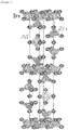
- FIG 1 a structure of InAlO 3 (ZnO) 4 is illustrated in FIG 1 .
- FIG 2 A structure of InGaO 3 (ZnO) 4 is illustrated in FIG 2 .
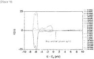
- DOS Density of State
- nAlO 3 (ZnO) 4 and InGaO 3 (ZnO) 4 are illustrated in FIGS. 3 and 5 , respectively
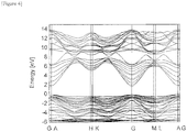
- band structures of the nAlO 3 (ZnO) 4 and InGaO 3 (ZnO) 4 are illustrated in FIGS. 4 and 6 , respectively.
- VBM valence band maximum
- CBM conduction band minimum
- the band structure exhibits energy levels of electrons at lattice points in a reciprocal space, and "0" on the vertical axis refers to Fermi energy.
- a valence band refers to bands lower than the Fermi energy and a conduction band refers to bands higher than the Fermi energy.
- a reciprocal number of a second derivative with respect to the reciprocal space having the horizontal aixs of bands refers to an effective mass of an electron
- an example material of the present application has a high curvature of the conduction band with reference to a G point (gamma point).
- LuFeO 3 (ZnO) n (n: 1, 4, 5, or 6) is illustrated in FIG. 9 .
- FIG. 9 illustrates a case where the n is 1, (b) illustrates case where the n is 4, (c) illustrates a case where the n is 5, (d) illustrates a case where the n is 6, and (e) illustrates a structure of ZnO.
- the compound of Chemical Formula 1 is doped with an additional element.
- the compound represented by Chemical Formula 1 is additionally doped with an n-type dopant.
- the n-type dopant comprises at least one selected from the group consisting of Sn, Ge, and Mo.
- InAlSnO 3 (ZnO) 4 obtained by additionally doping the InAlO 3 (ZnO) 4 with Sn, a mobility may be increased as compared with the InAlO 3 (ZnO) 4 ( ⁇ 10 cm2/Vsec).
- the compound represented by Chemical Formula 1 may be additionally doped with a p-type dopant.
- the p-type dopant may be a nitrogen atom but may not be limited thereto.
- N-doped InAlO 3 (ZnO) 4 As a compound obtained by additionally doping the compound represented by Chemical Formula 1 with a p-type dopant, there is an N-doped InAlO 3 (ZnO) 4 .
- the N-doped InAlO 3 (ZnO) 4 may be represented by InAlO 3 (ZnO) 4 :N.
- FIG. 10 A density of state of the N-doped InAlO 3 (ZnO) 4 is illustrated in FIG. 10 , and a structure of the N-doped InAlO 3 (ZnO) 4 is illustrated in FIG. 11 .
- a p-orbital component of N doping an O-site exhibits a p-type characteristic illustrated right above a VBM.
- a content range of an element in the compound of Chemical Formula 1, a content range of an additional doping element, etc. can be regulated in various ways to be suitable for purpose.
- an electronic element comprising the transparent conductive film.
- the transparent conductive film according to the present application can be used as a common electrode or pixel electrode of a liquid crystal display, an electrochromic display (ECD, an organic electroluminescence device, a solar cell, a plasma display panel, a flexible display, electronic paper, a touch panel, and the like.
- ECD electrochromic display
- organic electroluminescence device a solar cell
- plasma display panel a flexible display
- electronic paper a touch panel, and the like.
- a thin film transistor comprising the transparent conductive film.
- the transparent conductive film according to the present application can be used as a source electrode, a drain electrode, and a gate electrode of a thin film transistor and also used as an active layer and a gate insulating layer. That is, any one of the components of the thin film transistor can be formed of the transparent conductive film according to the present application or all of the components of the thin film transistor can be formed of the transparent conductive film according to the present application. Accordingly, a circuit of a smart window can be formed.
- FIG. 12 A structure of a thin film transistor according to the present application is illustrated in FIG. 12 .
- FIG. 12 schematically illustrates a thin film transistor employing InAlO 3 (ZnO) 4 and InGaO 3 (ZnO) 4 .
- the thin film transistor may comprise a gate electrode, a gate insulating layer, an active layer, a source electrode, and a drain electrode on a substrate.
- the gate electrode, the gate insulating layer, the active layer, the source electrode, and the drain electrode may comprise the compound represented by Chemical Formula 1 or a compound obatined by additionally doping the the compound represented by Chemical Formula 1 with the n-type dopant or the p-type dopant.
- the gate electrode may comprise InAlSnO 3 (ZnO) 4
- the gate insulating layer may comprise InGaO 3 (ZnO) 4
- the active layer may comprise a first active layer and a second active layer, and the first active layer may comprise InGaO 3 (ZnO) 4 :N and the second active layer may comprise InAlO 3 (ZnO) 4 :N.
- the source electrode and the drain electrode may comprise InAlSnO 3 (ZnO) 4 .
- npn-type transistor may have a lattice value mismatiching of less than about 1.3%.
- a thickness of the gate insulating layer may be 150 nm or less, and a thickness of each active layer may be 10 to 50 nm.
- the thin film transistor may have a threshold voltage of ⁇ 1.3 V, an on-off ratio of greater than 105, a field effect mobility of ⁇ 10 cm 2 /Vsec.
- the compound represented by Chemical Formula 1 of the present application is applied to manufacturing films using a crystal growth method such as a molecular beam epitaxy method, and, thus, chemcial, electrical, and optical properties thereof may be stable and superior to a conventionally known element using an amorphous material.
- a method for preparing the transparent conductive film according to the present application comprises forming, on a subtrate, a compound having a crystalline structure and represented by Chemical Formula 1.
- the transparent conductive film is prepared by using a DC/RF magnetron sputtering method or a molecular beam epitaxy method.
- the DC/RF magnetron sputtering method can be used in a chamber (usually maintained at 10 -3 to 10 -8 torr) equipped with In 2 O 3 , Al 2 O 3 , ZnO, Ga 2 O 3 sputter targets or a target having a chemical composition of InAlO 3 (ZnO) 4 or InGaO 3 (ZnO) 4 at a qualitative ratio by introducing a processing gas (O 2 , N 2 , etc.) of 10 -2 to 10 -3 torr into the chamber.
- a processing gas O 2 , N 2 , etc.
- the magnetron sputtering method can be applied to a roll-to-roll process. In this case, a thickness of the transparent conductive film can be adjusted to 10 nm to 10 ⁇ m.
- the substrate can be employed from those known in the art without limitation.
- the subtrate may be a glass substrate, a plastic substrate, etc. but may not be limited thereto.
- a content of the X from the (RXO 3 ) m (AO) n is 50% or less of a content of the R. This is because In from the InAlO 3 (ZnO) 4 and the InGaO 3 (ZnO) 4 has a property of maintaining an octahedron layer of InO 2 , whereas Al or Ga as a material having a high reactivity has a property of breaking an octahedron structure. Nevertheless, such instability can be complemented by modulating a ZnO layer, which is a great advantage of the compound.
- the N is 1,3,5, or 7 and the n is 2,4, or 6, a rhomohedral lattice structure and a hexagonal lattice structure can be maintained well.
- a material having a structure of (RXO 3 ) m (AO) n comprising a specific example of the InAlO 3 (ZnO) 4 and the InGaO 3 (ZnO) 4 can be converted into an n-type TCO by using a dopant such as Sn, Ge, Mo, F, Ti, Zr, Hf, Nb, Ta, W, Te, B, Y, Sc, V, Si, etc.
- a dopant such as Sn, Ge, Mo, F, Ti, Zr, Hf, Nb, Ta, W, Te, B, Y, Sc, V, Si, etc.
- Such dopants can be substituted for the X of the (RXO 3 ) m (AO) n compound.
- an electronic band gap and an optical band gap can be varioulsy adjusted from at least 2.9 eV to 3.4 eV in a crystalline state and from at least 2.6 eV to 3.4 eV in an amorphous state.
- a material of a specific example of the InAlO 3 (ZnO) 4 and the InGaO 3 (ZnO) 4 can be used for a gate insulator (thickness of ⁇ 150 nm) of a circuit element as a key component of AMOLED, Flat Panel Display, and various optoelectronics, and can be used for an active layer (thickness of 10 to 50 nm) through n-type doping.
- a conductive film containing InAlO 3 (ZnO) 4 or InGaO 3 (ZnO) 4 (not according to the invention) was prepared to a thickness of 50 nm.
- a roll-to-roll process was applied using a DC/RF magnetron sputtering evaporator.
- a vacuum level of a chamber system was usually maintained at 10 -5 torr.
- In 2 O 3 , Al 2 O 3 , ZnO, Ga 2 O 3 sputter targets (1,600 x 125 mm 2 , ⁇ 3.5 KW power applied) were installed at the evaporator and spaced 70 to 75 mm apart from a plastic substrate (eg. PET, PC having a width of 1,050 mm).
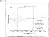
- Optical transmittance of the conductive film was obtained by a hybrid method (HSE06 method) and a result thereof is illustrated in FIG 7 . Electrical conductivity is illustrated in FIG 8 .
- transmittance of visible light was as high as 87 to 91%. Further, at room temperature (300K), electrical conductivity of the conductive film containing InAlO 3 (ZnO) 4 was about 10 -3 S/cm and electrical conductivity of the conductive film containing InGaO 3 (ZnO) 4 was about 10 -4 S/cm.
Landscapes
- Chemical & Material Sciences (AREA)
- Organic Chemistry (AREA)
- Inorganic Chemistry (AREA)
- Physics & Mathematics (AREA)
- Electromagnetism (AREA)
- Engineering & Computer Science (AREA)
- Manufacturing & Machinery (AREA)
- Non-Insulated Conductors (AREA)
- Thin Film Transistor (AREA)
- Physical Vapour Deposition (AREA)
- Composite Materials (AREA)
- Materials Engineering (AREA)
- Manufacturing Of Electric Cables (AREA)
- Electrodes Of Semiconductors (AREA)
- Photovoltaic Devices (AREA)
Description
- The present invention relates to a transparent conductive film and a method for preparing the same.
- A transparent conductive film refers to a thin film having high light transmittance and an electrically conductive property and has been widely used as a voltage apply type common electrode or pixel electrode of a liquid crystal display, an electrochromic display (ECD, an organic electroluminescence device, a solar cell, a plasma display panel, a flexible display, electronic paper, a touch panel, and the like.
- As for transparent conducting oxides (TCOs), it is important to design a material which transmits light in the visible ray area and has high conductivity In order to be transparent in the visible ray area (wavelength of 400 to 700 nm), an electronic energy band gap needs to be 3.1 eV or more equivalent to electromagnetic wave energy having a wavelength of 400 nm.
- As representative oxide semiconductors satisfying such properties, there are ZnO (3.3eV), In2O3 (3.7eV), and SnO2 (3.6eV). Typically, the TCO has light transmittance of 80% or more in the visible ray area and specific resistance of about 10-4 Ωcm or less as an electrical property.
- In order to find a material used for such TCOs, there has been mainly conducted research in which various materials are doped or alloyed. In particular, In2O3 has the specific resistance lower than that of SnO2 or ZnO, and, thus, it was the first to be commercialized. ITO (Sn doped In2O3) has been used so far.
- The ITO is a material having been used for an electrode for display in an LED, an LCD, a PDP, etc., a solar cell, and the like and has the low specific resistance of 10-4 Ωcm in general or 10-5 Ωcm in lab-scale which is close to specific resistance of metal.
- However, the ITO has the disadvantage of high price since In is one of rare elements, and if it is exposed to hydrogen plasma often used in a flat panel display manufacturing process, In or Sn is reduced and electrical and optical properties may be deteriorated. Further, it is known that the ITO is an n-type semiconductor and cannot be converted into a p-type semiconductor. For this reason, it is impossible to constitute a homo junction circuit element with the ITO only.
US2011/177696 A1 discloses a crystalline structure comprising InAlZnO4 or InAlO3(ZnO)2 crystal. These crystals may be used as a sputtering target for manufacturing conductive films. - In the pertinent technical field, there is in need of research on a transprent conductive film which has excellent properties and can be easily prepared and a method for preparing the same.
- Accoridng to one aspect of the present application, there is provided a transparent conductive filmcomprising a compound having a crystalline structure and represented by Chemical Formula 1,
wherein the compound represented by Chemical Formula 1 is additionally doped with an n-type dopant, and
wherein the n-type dopant comprises at least one selected from the group consisting of Sn, Ge, and Mo:
[Chemical Formula 1] [(RpXq)O3]m(AO)n
where, - R is Sc, Fe, Cu, Ga, Y, In, Er, Tm, Yb, or Lu,
- X is Al,
- a content of the X is 50% or less of a content of the R, and
- A is Mg, Mn, Co, or Zn,
- m is 1 to 4,
- n is 1 to 7, and
- p and q represent an atom content ratio of greater than 0 to 1 or less independently of each other.
- Further, according to another aspect of the present application, there is provided a method for preparing a transparent conductive film comprising forming, on a substrate, a compound having a crystalline structure and represented by Chemical Formula 1
wherein the forming a compound represented by Chemical Formula 1 uses a DC/RF magnetron sputtering method or a molecular beam epitaxy method,
wherein the compound represented by Chemical Formula 1 is additionally doped with an n-type dopant, and
wherein the n-type dopant comprises at least one selected from the group consisting of Sn, Ge, and Mo:
[Chemical Formula 1] [(RpXq)O3]m(AO)n
where, - R is Sc, Fe, Cu, Ga, Y, In, Er, Tm, Yb, or Lu,
- X is Al,
- a content of the X is 50% or less of a content of the R, and
- A is Mg, Mn, Co, or Zn,
- m is 1 to 4,
- n is 1 to 7, and
- p and q represent an atom content ratio of greater than 0 to 1 or less independently of each other.
- Furthermore, according to still another aspect of the present application, there is provided an electronic element comprising the transparent conductive film.
- Furthermore, according to still another aspect of the present application, there is provided a thin film transistor comprising the transparent conductive film.
Further embodiments are disclosed in the sub-claims. - A transparent conductive film according to an exemplary embodiment of the present application comprises a compound having a crystalline structure and represented by Chemical Formula 1 and thus has excellent conductivity and transmittance. Further, the transparent conductive film according to an exemplary embodiment of the present application has excellent elasticity and adhesive strength. Furthermore, the transparent conductive film according to an exemplary embodiment of the present application has a low haze value. Therefore, the transparent conductive film according to the present application can be applied as a technology substituting for conventional ITO conductive films.
-
-
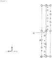
FIG 1 illustrates a structure of InAlO3(ZnO)4 according to an exemplary embodiment of the present application. -
FIG 2 illustrates a structure of InGaO3(ZnO)4. -
FIG. 3 illustrates a DOS (Density of State) of InAlO3(ZnO)4 according to an exemplary embodiment of the present application. -
FIG. 4 illustrates a band structure of InAlO3(ZnO)4 according to an exemplary embodiment of the present application. -
FIG. 5 illustrates a DOS (Density of State) of InGaO3(ZnO)4. -
FIG 6 illustrates a band structure of InGaO3(ZnO)4. -
FIG. 7 illustrates optical transmittance of a conductive film according to an exemplary embodiment of the present application. -
FIG. 8 illustrates electrical transmittance of a conductive film according to an exemplary embodiment of the present application. -
FIG. 9 illustrates a structure of LuFeO3(ZnO)n(n: 1,4,5, or 6). -
FIG. 10 illustrates a density of state of N-doped InAlO3(ZnO)4 according to an exemplary embodiment of the present application. -
FIG. 11 illustrates a structure of N-doped InAlO3(ZnO)4 according to an exemplary embodiment of the present application. -
FIG 12 illustrates a structure of a thin film transistor according to an exemplary embodiment of the present application. - Hereinafter, the present appication will be explaiend in detail.
- The present application can be applied to next-generation flexible devices, transparent AMOLED, OLED lighting, and solar cells as well as the industry of flat panel display devices such as LCD, PDP, and the like.
- A transparent oxide semiconductor is very important as a key technolgy of the transparent electronics technolgoy because the use of materials such as ITO (Sn-doped In2O3) and ZnO used as trnaprent electrodes of conventioanl optoelectronic devices is really considerable. In the case of the ITO as an n-type transparent electrode, its market is expected to grow to USD 6.9 billion (about 8.4 trillion won) by 2016.
- It is well known that ITO or AZO (Al-doped ZnO) as the prototype of conventional n-type TCOs has been intensively reserached and developed experimentally and theoretically. This is because such materials have high electrical conductivity and high transission of photon and also have a metal s-orbial that exhibits spatial delocalization of a conduction band, and low energy, low effecitve mass, as an electronic structural property in common to n-type TCO materials. For example, cations such as Zn(II), Ga(III), and In(III) in a closed-shell ns 0 state are bonded to oxides.
- Further, Ga-doped ZnO or F-doped SnO2 has been known as a TCO material. It is known that thses materilas have a carrier concentration (N(cm-3)) of 1016 to 1021 and an electron mobility (µ(cm2V-1s-1)) of about 10 to about 1,000.
- In contradistinciton to the delocalized conduction band, valence band state exhibits a localized O 2p state. Such a deep localized state involves local lattaic distortion, resulting in formation of a small polaron (a quasiparticle derived from an electric charge or an electric field).
- Furhter, a hole conducting p-type TCO material has a structure which can transmit a hole since a metal such as Cu(I) has a low bond energy at a valence band maximum (VBM). However, its hole mobility is as low as less than 10 cm2V-1s-1 due to an effect of a d band of localized metal such as Cu and existence of an indirect band gap.
- In order to produce a new material compatible with various optoelectronic applications and requiring cheap raw material cost as compared with conventional TCOs, there has been conducted research on TCOs having various strucutres. As a new TCO material candidate, a ternary compound and binary compound such as ZnO-In2O3-SnO2 system, ZnO-In2O3(IZO), and the like have been researched. However, we need to take note of TCO materials having more physicochemically stable and electrically and optically excellent properties. For example, there may be a homologous compound of which an ectronic structure can be calculated by density functional theory (DFT), super lattice which can demonstrate an electromagnetical applicability, and a material having a minimum interfacial strain and complying with the octet rule.
- It is not too much to say that the final technical objective of such materials used in the transparent electronics is how to manufacure a transparent homo junction. Since all of the conventional transparent electrodes or devices use hetero junction, an electro rectifying voltage is low and an electrical mobility of the hetero junction is inferior to that of the homo junction. Therefore, the ultimate method to solve such a problem is to find a semiconductor material which can be bipolar doped.
- Accordingly, a transparent conductive film according to an exemplary embodiment of the present application comprisesa compound having a crystalline structure and represented by Chemical Formula 1, wherein the compound represented by Chemical Formula 1 is additionally doped with an n-type dopant, and wherein the n-type dopant comprises at least one selected from the group consisting of Sn, Ge, and Mo:
[Chemical Formula 1] [(RpXq)O3]m(AO)n
where, - R is Sc, Fe, Cu, Ga, Y, In, Er, Tm, Yb, or Lu,
- X is Al,
- a content of the X is 50% or less of a content of the R, and
- A is Mg, Mn, Co, or Zn,
- m is 1 to 4,
- n is 1 to 7, and
- p and q represent an atom content ratio of greater than 0 to 1 or less independently of each other.
- In the present application, desirably, the A of Chemical Formula 1 may be Zn but may not be limited thereto.
- In the present application, desirably, the compound represented by Chemical Formula 1 may be InAlO3(ZnO)n, and the n may be 1 to 7 but may not be limited thereto.
- In Chemical Formula 1, if the n is an odd number, the compound may have a rhomohedral (R3m) strucutre, and if the n is an even number, the compound may have a hexagonal polymorph (P63 /mmc) structure.
- In particular, the compound represented by Chemical Formula 1 has a crystalline structure. As described above, since the compound represented by Chemical Formula 1 has a crystalline structure, it can satisfy transparency, conductivity, etc. as required in the art. Further, by additionally doping the compound represented by Chemical Formula 1 with an n-type dopant, a p-type dopant, etc., if necessary, transparency and elctrical properties of the compound represented by Chemical Formula 1 can be regulated.
- To be more specific, as an exemplary embodiment of the present application, a structure of InAlO3(ZnO)4 is illustrated in
FIG 1 . A structure of InGaO3(ZnO)4 is illustrated inFIG 2 . - The optimized lattice constants of InGaO3(ZnO)4 and InAlO3(ZnO)4 are listed in Table 1 below.
[Table 1] a c InGaO3(ZnO)4 3.308 Å 32.962 Å InAlO3(ZnO)4 3.266 Å 33.010 Å - Further, the DOS (Density of State) of InAlO3(ZnO)4 and InGaO3(ZnO)4 are illustrated in
FIGS. 3 and5 , respectively, and the band structures of the nAlO3(ZnO)4 and InGaO3(ZnO)4 are illustrated inFIGS. 4 and6 , respectively. - In
FIGS. 3 and5 , "0" on the horizontal axis of the DOS graph refers to Fermi energy of each material, and a valence band refers to bands of energy lower than the Fermi energy, and a conduction band refers to bands of energy higher than the Fermi energy. A valence band maximum (VBM) is formed of a p-orbital of oxygen of each material and a conduction band minimum (CBM) is formed of s-orbitals of respective aluminum and gallium. - In
FIGS. 4 and6 , the band structure exhibits energy levels of electrons at lattice points in a reciprocal space, and "0" on the vertical axis refers to Fermi energy. A valence band refers to bands lower than the Fermi energy and a conduction band refers to bands higher than the Fermi energy. Since a reciprocal number of a second derivative with respect to the reciprocal space having the horizontal aixs of bands refers to an effective mass of an electron, an example material of the present application has a high curvature of the conduction band with reference to a G point (gamma point). Thus, it can be seen that if a free electron is generated by n-type doping due to a low effective mass of the electron, a mobility of the free electron is high. - Further, a structure of LuFeO3(ZnO)n (n: 1, 4, 5, or 6) is illustrated in
FIG. 9 . - In
FIG. 9 , (a) illustrates a case where the n is 1, (b) illustrates case where the n is 4, (c) illustrates a case where the n is 5, (d) illustrates a case where the n is 6, and (e) illustrates a structure of ZnO. - In the structures of
FIG 9 , lutetium (Lu) atoms present in an octahedral cavity and iron (Fe) atoms and zinc (Zn) atoms present in a tetrahedral cavity are closely packed with oxygen (O) atoms. In 1980s, N. Kimizuka et al. tried to synthesize a LuFeO3-ZnO system. In order to manufacture a crystalline structure, they tried to grow Lu2O3, Fe2O3, and ZnO powder by using a solid-state reaction method. However, there is no record indicating that a crystalline material of precise stoichiometry was obtained. - Main factors of a crystal system of LuFeO3(ZnO) are as follows:
- Crystal system: Trigonal R3m
- Lattice constant: a = 3.4185 Å, c = 25.463 Å
- Main factors of a crystal system of LuFeO3(ZnO)4 are as follows:
- Crystal system: Hexagonal P63/mmc
- Lattice constant: a = 3.3406 Å, c = 32.51 Å
- Main factors of a crystal system of LuFeO3(ZnO)5 are as follows:
- Crystal system: Trigonal R3m
- Lattice constant: a = 3.3291 Å, c = 56.56 Å
- Main factors of a crystal system of LuFeO3(ZnO)6 are as follows:
- Crystal system: Hexagonal P63/mmc
- Lattice constant: a = 3.3220 Å, c = 42.91 Å
- Further, in the transparent conductive film according to the present application, the compound of Chemical Formula 1 is doped with an additional element.
- To be more specific, the compound represented by Chemical Formula 1 is additionally doped with an n-type dopant. The n-type dopant comprises at least one selected from the group consisting of Sn, Ge, and Mo.
- For example, the InAlO3(ZnO)4 itself can be applied as an n-type semiconductor (band gap energy Eg = 2.93eV). In the case of InAlSnO3(ZnO)4 obtained by additionally doping the InAlO3(ZnO)4 with Sn, a mobility may be increased as compared with the InAlO3(ZnO)4 (∼ 10 cm2/Vsec).
- Further, the compound represented by Chemical Formula 1 may be additionally doped with a p-type dopant. The p-type dopant may be a nitrogen atom but may not be limited thereto.
- For example, as a compound obtained by additionally doping the compound represented by Chemical Formula 1 with a p-type dopant, there is an N-doped InAlO3(ZnO)4. In the present specification, the N-doped InAlO3(ZnO)4 may be represented by InAlO3(ZnO)4:N. The N-doped InAlO3(ZnO)4 has lattice constants of a = 3.221 Å and c = 32.789 Å decreased by 1.4% on the a-axis and by 0.7% on the c-axis as compared with InAlO3(ZnO)4, and, thus, the N-doped InAlO3(ZnO)4 has a small strain in the structure caused by doping.
- A density of state of the N-doped InAlO3(ZnO)4 is illustrated in
FIG. 10 , and a structure of the N-doped InAlO3(ZnO)4 is illustrated inFIG. 11 . - Referring to
FIG 10 , it can be seen that a p-orbital component of N doping an O-site exhibits a p-type characteristic illustrated right above a VBM. - In the transparent conductive film according to the present application, a content range of an element in the compound of Chemical Formula 1, a content range of an additional doping element, etc. can be regulated in various ways to be suitable for purpose.
- Further, according to another aspect of the present application, there is provided an electronic element comprising the transparent conductive film.
- The transparent conductive film according to the present application can be used as a common electrode or pixel electrode of a liquid crystal display, an electrochromic display (ECD, an organic electroluminescence device, a solar cell, a plasma display panel, a flexible display, electronic paper, a touch panel, and the like.
- Further, according to still another aspect of the present application, there is provided a thin film transistor comprising the transparent conductive film.
- Furthermore, the transparent conductive film according to the present application can be used as a source electrode, a drain electrode, and a gate electrode of a thin film transistor and also used as an active layer and a gate insulating layer. That is, any one of the components of the thin film transistor can be formed of the transparent conductive film according to the present application or all of the components of the thin film transistor can be formed of the transparent conductive film according to the present application. Accordingly, a circuit of a smart window can be formed.
- A structure of a thin film transistor according to the present application is illustrated in
FIG. 12 . -
FIG. 12 schematically illustrates a thin film transistor employing InAlO3(ZnO)4 and InGaO3(ZnO)4. - To be more specific, the thin film transistor may comprise a gate electrode, a gate insulating layer, an active layer, a source electrode, and a drain electrode on a substrate. The gate electrode, the gate insulating layer, the active layer, the source electrode, and the drain electrode may comprise the compound represented by Chemical Formula 1 or a compound obatined by additionally doping the the compound represented by Chemical Formula 1 with the n-type dopant or the p-type dopant.
- The gate electrode may comprise InAlSnO3(ZnO)4, and the gate insulating layer may comprise InGaO3(ZnO)4. Further, the active layer may comprise a first active layer and a second active layer, and the first active layer may comprise InGaO3(ZnO)4:N and the second active layer may comprise InAlO3(ZnO)4:N. Furthermore, the source electrode and the drain electrode may comprise InAlSnO3(ZnO)4.
- That is, tin (Sn) is used as the n-type dopant and nitrogen (N) is used as the p-type dopant. Such an npn-type transistor may have a lattice value mismatiching of less than about 1.3%. A thickness of the gate insulating layer may be 150 nm or less, and a thickness of each active layer may be 10 to 50 nm.
- As physical properties, the thin film transistor may have a threshold voltage of ∼1.3 V, an on-off ratio of greater than 105, a field effect mobility of ∼10 cm2/Vsec.
- The compound represented by Chemical Formula 1 of the present application is applied to manufacturing films using a crystal growth method such as a molecular beam epitaxy method, and, thus, chemcial, electrical, and optical properties thereof may be stable and superior to a conventionally known element using an amorphous material.
- Further, a method for preparing the transparent conductive film according to the present application comprises forming, on a subtrate, a compound having a crystalline structure and represented by Chemical Formula 1.
- To be more specific, the transparent conductive film is prepared by using a DC/RF magnetron sputtering method or a molecular beam epitaxy method.
- The DC/RF magnetron sputtering method can be used in a chamber (usually maintained at 10-3 to 10-8 torr) equipped with In2O3, Al2O3, ZnO, Ga2O3 sputter targets or a target having a chemical composition of InAlO3(ZnO)4 or InGaO3(ZnO)4 at a qualitative ratio by introducing a processing gas (O2, N2, etc.) of 10-2 to 10-3 torr into the chamber. In particular, the magnetron sputtering method can be applied to a roll-to-roll process. In this case, a thickness of the transparent conductive film can be adjusted to 10 nm to 10 µm.
- In the case of using the molecular beam epitaxy method, with grains of metal, such as In, Al, and Ga, having a high purity (99.999% or more), metal atoms ionized at a high temperature by using an effusion cell can be epitaxied on a substrate at 10-4 to 10-6 tor together with oxygen plasma beam in a chamber (usually maintained at 10-8 torr or less). As a result, a film (thickness of 0.2 to 2,000 nm) at a single crystal level can be obtained.
- In the present application, the substrate can be employed from those known in the art without limitation. To be more specific, the subtrate may be a glass substrate, a plastic substrate, etc. but may not be limited thereto.
- In the compound having a structure of (RXO3)m(AO)n as a new TCO material, its characteristic may begin with modulating a ratio between (RXO3)m and (AO)n. That is, as a specific example, it is confirmed that the InAlO3(ZnO)4 and the InGaO3(ZnO)4 is modulated at a ratio of 1 : 4. Typically, when m of the (RXO3)m is fixed to 1 and n of the (AO)n varies, the most stable DOS (Density of State) can be obtained. Since the (RXO3)m and the (AO)n are bonded to each other, both transparent conductivity and photoelectric applicability can be obtained simultaneously.
- A content of the X from the (RXO3)m(AO)n is 50% or less of a content of the R. This is because In from the InAlO3(ZnO)4 and the InGaO3(ZnO)4 has a property of maintaining an octahedron layer of InO2, whereas Al or Ga as a material having a high reactivity has a property of breaking an octahedron structure. Nevertheless, such instability can be complemented by modulating a ZnO layer, which is a great advantage of the compound. When the N is 1,3,5, or 7 and the n is 2,4, or 6, a rhomohedral lattice structure and a hexagonal lattice structure can be maintained well.
- A material having a structure of (RXO3)m(AO)n comprising a specific example of the InAlO3(ZnO)4 and the InGaO3(ZnO)4 can be converted into an n-type TCO by using a dopant such as Sn, Ge, Mo, F, Ti, Zr, Hf, Nb, Ta, W, Te, B, Y, Sc, V, Si, etc. Such dopants can be substituted for the X of the (RXO3)m(AO)n compound. By adjusting the dopant and a ratio of m:n, an electronic band gap and an optical band gap can be varioulsy adjusted from at least 2.9 eV to 3.4 eV in a crystalline state and from at least 2.6 eV to 3.4 eV in an amorphous state.
- In particular, a material of a specific example of the InAlO3(ZnO)4 and the InGaO3(ZnO)4 can be used for a gate insulator (thickness of ∼150 nm) of a circuit element as a key component of AMOLED, Flat Panel Display, and various optoelectronics, and can be used for an active layer (thickness of 10 to 50 nm) through n-type doping.
- Hereinafter, a desirble example will be provided to facilitate an understanding of the present application. However, the following example is provided for the purpose of illustration of the present application but not limits the scope of the present application.
- A conductive film containing InAlO3(ZnO)4 or InGaO3(ZnO)4 (not according to the invention) was prepared to a thickness of 50 nm. A roll-to-roll process was applied using a DC/RF magnetron sputtering evaporator. A vacuum level of a chamber system was usually maintained at 10-5 torr. In2O3, Al2O3, ZnO, Ga2O3 sputter targets (1,600 x 125 mm2, ∼3.5 KW power applied) were installed at the evaporator and spaced 70 to 75 mm apart from a plastic substrate (eg. PET, PC having a width of 1,050 mm). By additionally introducing an O2 gas, an oxygen atoms insufficient for vapor deposition were supplied. As a result, a transparent conductive film containing InAlO3(ZnO)4 and InGaO3(ZnO)4 at a qualitative ratio was obtained.
- Optical transmittance of the conductive film was obtained by a hybrid method (HSE06 method) and a result thereof is illustrated in
FIG 7 . Electrical conductivity is illustrated inFIG 8 . - As confirmed in the above results, transmittance of visible light was as high as 87 to 91%. Further, at room temperature (300K), electrical conductivity of the conductive film containing InAlO3(ZnO)4 was about 10-3 S/cm and electrical conductivity of the conductive film containing InGaO3(ZnO)4 was about 10-4 S/cm.
Claims (10)
- A transparent conductive film comprising a compound having a crystalline structure and represented by Chemical Formula 1,
wherein the compound represented by Chemical Formula 1 is additionally doped with an n-type dopant, and
wherein the n-type dopant comprises at least one selected from the group consisting of Sn, Ge, and Mo:
[Chemical Formula 1] [(RpXq)O3]m(AO)n
where,R is Sc, Fe, Cu, Ga, Y, In, Er, Tm, Yb, or Lu,X is Al,a content of the X is 50% or less of a content of the R, andA is Mg, Mn, Co, or Zn,m is 1 to 4,n is 1 to 7, andp and q represent an atom content ratio of greater than 0 to 1 or less independently of each other. - The transparent conductive film of claim 1, wherein the R of Chemical Formula 1 is In or Lu.
- The transparent conductive film of claim 1, wherein the compound represented by Chemical Formula 1 is InAlO3(ZnO)n, and the n is 1 to 7.
- A method for preparing a transparent conductive film comprising forming, on a substrate, a compound having a crystalline structure and represented by Chemical Formula 1
wherein the forming a compound represented by Chemical Formula 1 uses a DC/RF magnetron sputtering method or a molecular beam epitaxy method
wherein the compound represented by Chemical Formula 1 is additionally doped with an n-type dopant, and
wherein the n-type dopant comprises at least one selected from the group consisting of Sn, Ge, and Mo:
[Chemical Formula 1] [(RpXq)O3]m(AO)n
where,R is Sc, Fe, Cu, Ga, Y, In, Er, Tm, Yb, or Lu,X is Al,a content of the X is 50% or less of a content of the R, andA is Mg, Mn, Co, or Zn,m is 1 to 4,n is 1 to 7, andp and q represent an atom content ratio of greater than 0 to 1 or less independently of each other. - The method for preparing a transparent conductive film of claim 4, wherein the compound represented by Chemical Formula 1 is InAlO3(ZnO)n, and the n is 1 to 7.
- An electronic element comprising the transparent conductive film of any one of claims 1 to 3.
- A thin film transistor comprising the transparent conductive film of any one of claims 1 to 3.
- The thin film transistor of claim 7, wherein the thin film transistor comprises a gate electrode, a gate insulating layer, an active layer, a source electrode, and a drain electrode on a substrate, and
the gate electrode, the gate insulating layer, the active layer, the source electrode, and the drain electrode comprises the compound represented by Chemical Formula 1. - The thin film transistor of claim 8, wherein the gate electrode comprises InAlSnO3(ZnO)4.
- The thin film transistor of claim 8, wherein the source electrode and the drain electrode comprise InAlSnO3(ZnO)4.
Applications Claiming Priority (2)
| Application Number | Priority Date | Filing Date | Title |
|---|---|---|---|
| KR20120103498 | 2012-09-18 | ||
| PCT/KR2013/008444 WO2014046480A1 (en) | 2012-09-18 | 2013-09-17 | Transparent conducting film and preparation method thereof |
Publications (3)
| Publication Number | Publication Date |
|---|---|
| EP2866232A1 EP2866232A1 (en) | 2015-04-29 |
| EP2866232A4 EP2866232A4 (en) | 2016-04-06 |
| EP2866232B1 true EP2866232B1 (en) | 2018-03-07 |
Family
ID=50341701
Family Applications (1)
| Application Number | Title | Priority Date | Filing Date |
|---|---|---|---|
| EP13839469.7A Active EP2866232B1 (en) | 2012-09-18 | 2013-09-17 | Transparent conducting film and preparation method thereof |
Country Status (7)
| Country | Link |
|---|---|
| US (1) | US9577109B2 (en) |
| EP (1) | EP2866232B1 (en) |
| JP (1) | JP6080141B2 (en) |
| KR (1) | KR101472219B1 (en) |
| CN (1) | CN104584139B (en) |
| TW (1) | TWI543195B (en) |
| WO (1) | WO2014046480A1 (en) |
Families Citing this family (8)
| Publication number | Priority date | Publication date | Assignee | Title |
|---|---|---|---|---|
| CN104167448B (en) * | 2014-08-05 | 2017-06-30 | 京东方科技集团股份有限公司 | Thin film transistor (TFT) and preparation method thereof, array base palte and display device |
| DE102015213305A1 (en) | 2015-07-15 | 2017-01-19 | Saint-Augustin Canada Electric Inc. | A light transmission optical element for a solar energy device having a crop region and an alignment control region, and methods of adjusting same |
| CN106711201B (en) * | 2016-10-20 | 2020-01-17 | 浙江大学 | A p-type CrMCuO amorphous oxide semiconductor thin film and preparation method thereof |
| CN106711202A (en) * | 2016-10-20 | 2017-05-24 | 浙江大学 | P-type ZnAlSnO amorphous oxide semiconductor film and manufacturing method thereof |
| CN106711195B (en) * | 2016-10-20 | 2020-01-17 | 浙江大学 | A kind of p-type ZnMSnO amorphous oxide semiconductor thin film and preparation method thereof |
| CN106711228B (en) * | 2016-10-20 | 2020-03-03 | 浙江大学 | A p-type LaMSnO amorphous oxide semiconductor thin film and preparation method thereof |
| US11056593B2 (en) | 2017-09-12 | 2021-07-06 | Intel Corporation | Semiconductor devices with metal contacts including crystalline alloys |
| CN113135600B (en) * | 2021-03-03 | 2022-05-13 | 重庆文理学院 | Preparation method of amorphous iron oxide film |
Family Cites Families (17)
| Publication number | Priority date | Publication date | Assignee | Title |
|---|---|---|---|---|
| JP3945887B2 (en) * | 1998-01-30 | 2007-07-18 | Hoya株式会社 | Article having conductive oxide thin film and method for producing the same |
| JP3423896B2 (en) | 1999-03-25 | 2003-07-07 | 科学技術振興事業団 | Semiconductor devices |
| JP3531865B2 (en) * | 2000-07-06 | 2004-05-31 | 独立行政法人 科学技術振興機構 | Ultra-flat transparent conductive film and manufacturing method thereof |
| EP1443130B1 (en) * | 2001-11-05 | 2011-09-28 | Japan Science and Technology Agency | Natural superlattice homologous single crystal thin film, method for preparation thereof, and device using said single crystal thin film |
| JP3803592B2 (en) * | 2002-02-26 | 2006-08-02 | 株式会社アルバック | Low resistance transparent conductive film and method for producing the same |
| EP2413366B1 (en) * | 2004-03-12 | 2017-01-11 | Japan Science And Technology Agency | A switching element of LCDs or organic EL displays |
| RU2369940C2 (en) | 2004-11-10 | 2009-10-10 | Кэнон Кабусики Кайся | Amorphous oxide and field-effect transistor using said oxide |
| JP4836229B2 (en) * | 2005-05-31 | 2011-12-14 | 株式会社東芝 | Phosphor and light emitting device |
| JP5058469B2 (en) * | 2005-09-06 | 2012-10-24 | キヤノン株式会社 | Sputtering target and method for forming a thin film using the target |
| JP2009123957A (en) | 2007-11-15 | 2009-06-04 | Sumitomo Chemical Co Ltd | Oxide semiconductor material, manufacturing method thereof, electronic device, and field effect transistor |
| TWI532862B (en) | 2008-05-22 | 2016-05-11 | 出光興產股份有限公司 | A sputtering target, a method for forming an amorphous oxide film using the same, and a method for manufacturing a thin film transistor |
| KR101565196B1 (en) * | 2008-12-15 | 2015-11-02 | 이데미쓰 고산 가부시키가이샤 | Indium oxide sintered compact and sputtering target |
| JP5468801B2 (en) * | 2009-03-23 | 2014-04-09 | 株式会社カネカ | Substrate with transparent electrode and manufacturing method thereof |
| CN102473729B (en) | 2009-07-03 | 2015-01-28 | 株式会社半导体能源研究所 | Method for manufacturing semiconductor device |
| KR20110022813A (en) * | 2009-08-28 | 2011-03-08 | 삼성코닝정밀소재 주식회사 | Zinc Oxide Conductor and Manufacturing Method Thereof |
| JP5129392B2 (en) * | 2009-08-28 | 2013-01-30 | 株式会社東芝 | Method for producing phosphor and phosphor produced thereby |
| JP5708910B2 (en) | 2010-03-30 | 2015-04-30 | ソニー株式会社 | THIN FILM TRANSISTOR, MANUFACTURING METHOD THEREOF, AND DISPLAY DEVICE |
-
2013
- 2013-09-17 US US14/419,847 patent/US9577109B2/en active Active
- 2013-09-17 KR KR1020130112118A patent/KR101472219B1/en active Active
- 2013-09-17 EP EP13839469.7A patent/EP2866232B1/en active Active
- 2013-09-17 JP JP2015529700A patent/JP6080141B2/en active Active
- 2013-09-17 CN CN201380044464.6A patent/CN104584139B/en active Active
- 2013-09-17 WO PCT/KR2013/008444 patent/WO2014046480A1/en not_active Ceased
- 2013-09-18 TW TW102133810A patent/TWI543195B/en active
Non-Patent Citations (1)
| Title |
|---|
| None * |
Also Published As
| Publication number | Publication date |
|---|---|
| TW201426763A (en) | 2014-07-01 |
| CN104584139A (en) | 2015-04-29 |
| TWI543195B (en) | 2016-07-21 |
| EP2866232A4 (en) | 2016-04-06 |
| US20150194531A1 (en) | 2015-07-09 |
| KR20140036991A (en) | 2014-03-26 |
| JP6080141B2 (en) | 2017-02-15 |
| US9577109B2 (en) | 2017-02-21 |
| CN104584139B (en) | 2017-03-01 |
| KR101472219B1 (en) | 2014-12-11 |
| WO2014046480A1 (en) | 2014-03-27 |
| JP2015535881A (en) | 2015-12-17 |
| EP2866232A1 (en) | 2015-04-29 |
Similar Documents
| Publication | Publication Date | Title |
|---|---|---|
| US9577109B2 (en) | Transparent conducting film and preparation method thereof | |
| EP2537185B1 (en) | Field effect transistor, display element, image display device, and system | |
| Wang et al. | Effect of substrate temperature on transparent conducting Al and F co-doped ZnO thin films prepared by rf magnetron sputtering | |
| Fortunato et al. | Highly stable transparent and conducting gallium-doped zinc oxide thin films for photovoltaic applications | |
| US10366803B2 (en) | Metal oxide thin film, method for depositing metal oxide thin film and device comprising metal oxide thin film | |
| US20110141076A1 (en) | Semiconductor device, method for manufacturing semiconductor device, transistor substrate, light emitting device and display device | |
| Jayathilake et al. | Overview on transparent conducting oxides and state of the art of low-cost doped ZnO systems | |
| Wei et al. | Growth, Microstructures, and Optoelectronic Properties of Epitaxial BaSn1–x Sb x O3− δ Thin Films by Chemical Solution Deposition | |
| US8253012B2 (en) | High quality transparent conducting oxide thin films | |
| KR101183967B1 (en) | Functionally graded Transparent conducting oxide film and method for manufacturing thereof, Anode for Organic light emitting diode and window layer for solar cell using functionally graded transparent conducting oxide film | |
| US11624109B2 (en) | Method for manufacturing transparent conductive film | |
| US9546415B2 (en) | Composite transparent electrodes | |
| Lu et al. | Fabrication of low-resistive p-type Al–N co-doped zinc oxide thin films by RF reactive magnetron sputtering | |
| Liu et al. | Enhancing transparent thin-film transistor device performances by using a Ti-doped GaZnO channel layer | |
| US9666324B2 (en) | Transparent conductive thin film | |
| KR100733915B1 (en) | Transparent conductive oxide film in which buffer layer is deposited on polymer material substrate and manufacturing method thereof | |
| Chu et al. | Effect of annealing conditions on the structural, electrical and optical properties of Li-doped NiO thin films | |
| KR101807957B1 (en) | Highly conductive flexible transparent electrodes based oxide and method for manufacturing thereof | |
| KR20070021342A (en) | Method of manufacturing a metal doped thin film by controlling oxygen / argon flow rate ratio using magnetron sputtering | |
| Chen et al. | Improvement of Electrical and Wet-Etching Characteristics for Ingatio Electrodes in Organic Light-Emitting Diodes Through Hydrogen Doping | |
| KR20080016034A (en) | Method for manufacturing GZO thin film using magnetron sputtering | |
| Vásquez-A et al. | Study of the properties of n+-type ZnO: Al films obtained from ZnO/Al/ZnO nanometric structure |
Legal Events
| Date | Code | Title | Description |
|---|---|---|---|
| PUAI | Public reference made under article 153(3) epc to a published international application that has entered the european phase |
Free format text: ORIGINAL CODE: 0009012 |
|
| 17P | Request for examination filed |
Effective date: 20150123 |
|
| AK | Designated contracting states |
Kind code of ref document: A1 Designated state(s): AL AT BE BG CH CY CZ DE DK EE ES FI FR GB GR HR HU IE IS IT LI LT LU LV MC MK MT NL NO PL PT RO RS SE SI SK SM TR |
|
| AX | Request for extension of the european patent |
Extension state: BA ME |
|
| DAX | Request for extension of the european patent (deleted) | ||
| RA4 | Supplementary search report drawn up and despatched (corrected) |
Effective date: 20160303 |
|
| RIC1 | Information provided on ipc code assigned before grant |
Ipc: H01L 29/51 20060101ALI20160226BHEP Ipc: H01L 51/52 20060101ALI20160226BHEP Ipc: H01L 29/49 20060101ALI20160226BHEP Ipc: C01G 15/00 20060101ALI20160226BHEP Ipc: H01L 29/45 20060101ALI20160226BHEP Ipc: H01L 29/786 20060101ALI20160226BHEP Ipc: H01B 5/14 20060101ALI20160226BHEP Ipc: H01B 1/08 20060101AFI20160226BHEP Ipc: H01L 31/0224 20060101ALI20160226BHEP Ipc: H01L 51/44 20060101ALI20160226BHEP Ipc: H01B 13/00 20060101ALI20160226BHEP |
|
| 17Q | First examination report despatched |
Effective date: 20170210 |
|
| GRAP | Despatch of communication of intention to grant a patent |
Free format text: ORIGINAL CODE: EPIDOSNIGR1 |
|
| INTG | Intention to grant announced |
Effective date: 20180103 |
|
| RAX | Requested extension states of the european patent have changed |
Extension state: BA Extension state: ME |
|
| GRAS | Grant fee paid |
Free format text: ORIGINAL CODE: EPIDOSNIGR3 |
|
| GRAA | (expected) grant |
Free format text: ORIGINAL CODE: 0009210 |
|
| AK | Designated contracting states |
Kind code of ref document: B1 Designated state(s): AL AT BE BG CH CY CZ DE DK EE ES FI FR GB GR HR HU IE IS IT LI LT LU LV MC MK MT NL NO PL PT RO RS SE SI SK SM TR |
|
| DAX | Request for extension of the european patent (deleted) | ||
| REG | Reference to a national code |
Ref country code: GB Ref legal event code: FG4D |
|
| REG | Reference to a national code |
Ref country code: CH Ref legal event code: EP Ref country code: AT Ref legal event code: REF Ref document number: 977382 Country of ref document: AT Kind code of ref document: T Effective date: 20180315 |
|
| REG | Reference to a national code |
Ref country code: IE Ref legal event code: FG4D |
|
| REG | Reference to a national code |
Ref country code: DE Ref legal event code: R096 Ref document number: 602013034211 Country of ref document: DE |
|
| REG | Reference to a national code |
Ref country code: NL Ref legal event code: MP Effective date: 20180307 |
|
| REG | Reference to a national code |
Ref country code: LT Ref legal event code: MG4D |
|
| PG25 | Lapsed in a contracting state [announced via postgrant information from national office to epo] |
Ref country code: FI Free format text: LAPSE BECAUSE OF FAILURE TO SUBMIT A TRANSLATION OF THE DESCRIPTION OR TO PAY THE FEE WITHIN THE PRESCRIBED TIME-LIMIT Effective date: 20180307 Ref country code: LT Free format text: LAPSE BECAUSE OF FAILURE TO SUBMIT A TRANSLATION OF THE DESCRIPTION OR TO PAY THE FEE WITHIN THE PRESCRIBED TIME-LIMIT Effective date: 20180307 Ref country code: CY Free format text: LAPSE BECAUSE OF FAILURE TO SUBMIT A TRANSLATION OF THE DESCRIPTION OR TO PAY THE FEE WITHIN THE PRESCRIBED TIME-LIMIT Effective date: 20180307 Ref country code: HR Free format text: LAPSE BECAUSE OF FAILURE TO SUBMIT A TRANSLATION OF THE DESCRIPTION OR TO PAY THE FEE WITHIN THE PRESCRIBED TIME-LIMIT Effective date: 20180307 Ref country code: NO Free format text: LAPSE BECAUSE OF FAILURE TO SUBMIT A TRANSLATION OF THE DESCRIPTION OR TO PAY THE FEE WITHIN THE PRESCRIBED TIME-LIMIT Effective date: 20180607 Ref country code: ES Free format text: LAPSE BECAUSE OF FAILURE TO SUBMIT A TRANSLATION OF THE DESCRIPTION OR TO PAY THE FEE WITHIN THE PRESCRIBED TIME-LIMIT Effective date: 20180307 |
|
| REG | Reference to a national code |
Ref country code: AT Ref legal event code: MK05 Ref document number: 977382 Country of ref document: AT Kind code of ref document: T Effective date: 20180307 |
|
| REG | Reference to a national code |
Ref country code: FR Ref legal event code: PLFP Year of fee payment: 6 |
|
| PG25 | Lapsed in a contracting state [announced via postgrant information from national office to epo] |
Ref country code: RS Free format text: LAPSE BECAUSE OF FAILURE TO SUBMIT A TRANSLATION OF THE DESCRIPTION OR TO PAY THE FEE WITHIN THE PRESCRIBED TIME-LIMIT Effective date: 20180307 Ref country code: BG Free format text: LAPSE BECAUSE OF FAILURE TO SUBMIT A TRANSLATION OF THE DESCRIPTION OR TO PAY THE FEE WITHIN THE PRESCRIBED TIME-LIMIT Effective date: 20180607 Ref country code: SE Free format text: LAPSE BECAUSE OF FAILURE TO SUBMIT A TRANSLATION OF THE DESCRIPTION OR TO PAY THE FEE WITHIN THE PRESCRIBED TIME-LIMIT Effective date: 20180307 Ref country code: LV Free format text: LAPSE BECAUSE OF FAILURE TO SUBMIT A TRANSLATION OF THE DESCRIPTION OR TO PAY THE FEE WITHIN THE PRESCRIBED TIME-LIMIT Effective date: 20180307 Ref country code: GR Free format text: LAPSE BECAUSE OF FAILURE TO SUBMIT A TRANSLATION OF THE DESCRIPTION OR TO PAY THE FEE WITHIN THE PRESCRIBED TIME-LIMIT Effective date: 20180608 |
|
| PG25 | Lapsed in a contracting state [announced via postgrant information from national office to epo] |
Ref country code: IT Free format text: LAPSE BECAUSE OF FAILURE TO SUBMIT A TRANSLATION OF THE DESCRIPTION OR TO PAY THE FEE WITHIN THE PRESCRIBED TIME-LIMIT Effective date: 20180307 Ref country code: NL Free format text: LAPSE BECAUSE OF FAILURE TO SUBMIT A TRANSLATION OF THE DESCRIPTION OR TO PAY THE FEE WITHIN THE PRESCRIBED TIME-LIMIT Effective date: 20180307 Ref country code: EE Free format text: LAPSE BECAUSE OF FAILURE TO SUBMIT A TRANSLATION OF THE DESCRIPTION OR TO PAY THE FEE WITHIN THE PRESCRIBED TIME-LIMIT Effective date: 20180307 Ref country code: RO Free format text: LAPSE BECAUSE OF FAILURE TO SUBMIT A TRANSLATION OF THE DESCRIPTION OR TO PAY THE FEE WITHIN THE PRESCRIBED TIME-LIMIT Effective date: 20180307 Ref country code: AL Free format text: LAPSE BECAUSE OF FAILURE TO SUBMIT A TRANSLATION OF THE DESCRIPTION OR TO PAY THE FEE WITHIN THE PRESCRIBED TIME-LIMIT Effective date: 20180307 Ref country code: PL Free format text: LAPSE BECAUSE OF FAILURE TO SUBMIT A TRANSLATION OF THE DESCRIPTION OR TO PAY THE FEE WITHIN THE PRESCRIBED TIME-LIMIT Effective date: 20180307 |
|
| PG25 | Lapsed in a contracting state [announced via postgrant information from national office to epo] |
Ref country code: AT Free format text: LAPSE BECAUSE OF FAILURE TO SUBMIT A TRANSLATION OF THE DESCRIPTION OR TO PAY THE FEE WITHIN THE PRESCRIBED TIME-LIMIT Effective date: 20180307 Ref country code: SK Free format text: LAPSE BECAUSE OF FAILURE TO SUBMIT A TRANSLATION OF THE DESCRIPTION OR TO PAY THE FEE WITHIN THE PRESCRIBED TIME-LIMIT Effective date: 20180307 Ref country code: SM Free format text: LAPSE BECAUSE OF FAILURE TO SUBMIT A TRANSLATION OF THE DESCRIPTION OR TO PAY THE FEE WITHIN THE PRESCRIBED TIME-LIMIT Effective date: 20180307 Ref country code: CZ Free format text: LAPSE BECAUSE OF FAILURE TO SUBMIT A TRANSLATION OF THE DESCRIPTION OR TO PAY THE FEE WITHIN THE PRESCRIBED TIME-LIMIT Effective date: 20180307 |
|
| REG | Reference to a national code |
Ref country code: DE Ref legal event code: R097 Ref document number: 602013034211 Country of ref document: DE |
|
| PG25 | Lapsed in a contracting state [announced via postgrant information from national office to epo] |
Ref country code: PT Free format text: LAPSE BECAUSE OF FAILURE TO SUBMIT A TRANSLATION OF THE DESCRIPTION OR TO PAY THE FEE WITHIN THE PRESCRIBED TIME-LIMIT Effective date: 20180709 |
|
| PLBE | No opposition filed within time limit |
Free format text: ORIGINAL CODE: 0009261 |
|
| STAA | Information on the status of an ep patent application or granted ep patent |
Free format text: STATUS: NO OPPOSITION FILED WITHIN TIME LIMIT |
|
| PG25 | Lapsed in a contracting state [announced via postgrant information from national office to epo] |
Ref country code: DK Free format text: LAPSE BECAUSE OF FAILURE TO SUBMIT A TRANSLATION OF THE DESCRIPTION OR TO PAY THE FEE WITHIN THE PRESCRIBED TIME-LIMIT Effective date: 20180307 |
|
| 26N | No opposition filed |
Effective date: 20181210 |
|
| PG25 | Lapsed in a contracting state [announced via postgrant information from national office to epo] |
Ref country code: SI Free format text: LAPSE BECAUSE OF FAILURE TO SUBMIT A TRANSLATION OF THE DESCRIPTION OR TO PAY THE FEE WITHIN THE PRESCRIBED TIME-LIMIT Effective date: 20180307 |
|
| PG25 | Lapsed in a contracting state [announced via postgrant information from national office to epo] |
Ref country code: MC Free format text: LAPSE BECAUSE OF FAILURE TO SUBMIT A TRANSLATION OF THE DESCRIPTION OR TO PAY THE FEE WITHIN THE PRESCRIBED TIME-LIMIT Effective date: 20180307 |
|
| REG | Reference to a national code |
Ref country code: CH Ref legal event code: PL |
|
| REG | Reference to a national code |
Ref country code: BE Ref legal event code: MM Effective date: 20180930 |
|
| REG | Reference to a national code |
Ref country code: IE Ref legal event code: MM4A |
|
| PG25 | Lapsed in a contracting state [announced via postgrant information from national office to epo] |
Ref country code: LU Free format text: LAPSE BECAUSE OF NON-PAYMENT OF DUE FEES Effective date: 20180917 |
|
| PG25 | Lapsed in a contracting state [announced via postgrant information from national office to epo] |
Ref country code: IE Free format text: LAPSE BECAUSE OF NON-PAYMENT OF DUE FEES Effective date: 20180917 |
|
| PG25 | Lapsed in a contracting state [announced via postgrant information from national office to epo] |
Ref country code: BE Free format text: LAPSE BECAUSE OF NON-PAYMENT OF DUE FEES Effective date: 20180930 Ref country code: CH Free format text: LAPSE BECAUSE OF NON-PAYMENT OF DUE FEES Effective date: 20180930 Ref country code: LI Free format text: LAPSE BECAUSE OF NON-PAYMENT OF DUE FEES Effective date: 20180930 |
|
| PG25 | Lapsed in a contracting state [announced via postgrant information from national office to epo] |
Ref country code: MT Free format text: LAPSE BECAUSE OF NON-PAYMENT OF DUE FEES Effective date: 20180917 |
|
| PG25 | Lapsed in a contracting state [announced via postgrant information from national office to epo] |
Ref country code: TR Free format text: LAPSE BECAUSE OF FAILURE TO SUBMIT A TRANSLATION OF THE DESCRIPTION OR TO PAY THE FEE WITHIN THE PRESCRIBED TIME-LIMIT Effective date: 20180307 |
|
| PG25 | Lapsed in a contracting state [announced via postgrant information from national office to epo] |
Ref country code: HU Free format text: LAPSE BECAUSE OF FAILURE TO SUBMIT A TRANSLATION OF THE DESCRIPTION OR TO PAY THE FEE WITHIN THE PRESCRIBED TIME-LIMIT; INVALID AB INITIO Effective date: 20130917 |
|
| PG25 | Lapsed in a contracting state [announced via postgrant information from national office to epo] |
Ref country code: MK Free format text: LAPSE BECAUSE OF NON-PAYMENT OF DUE FEES Effective date: 20180307 |
|
| PG25 | Lapsed in a contracting state [announced via postgrant information from national office to epo] |
Ref country code: IS Free format text: LAPSE BECAUSE OF FAILURE TO SUBMIT A TRANSLATION OF THE DESCRIPTION OR TO PAY THE FEE WITHIN THE PRESCRIBED TIME-LIMIT Effective date: 20180707 |
|
| PGFP | Annual fee paid to national office [announced via postgrant information from national office to epo] |
Ref country code: DE Payment date: 20250820 Year of fee payment: 13 |
|
| PGFP | Annual fee paid to national office [announced via postgrant information from national office to epo] |
Ref country code: GB Payment date: 20250820 Year of fee payment: 13 |
|
| PGFP | Annual fee paid to national office [announced via postgrant information from national office to epo] |
Ref country code: FR Payment date: 20250821 Year of fee payment: 13 |