EP2858272A1 - Non-linear distortion compensator, method of compensating non-linear distortion, and optical receiver - Google Patents
Non-linear distortion compensator, method of compensating non-linear distortion, and optical receiver Download PDFInfo
- Publication number
- EP2858272A1 EP2858272A1 EP14182091.0A EP14182091A EP2858272A1 EP 2858272 A1 EP2858272 A1 EP 2858272A1 EP 14182091 A EP14182091 A EP 14182091A EP 2858272 A1 EP2858272 A1 EP 2858272A1
- Authority
- EP
- European Patent Office
- Prior art keywords
- linear distortion
- discriminator
- signal
- linear
- symbol
- Prior art date
- Legal status (The legal status is an assumption and is not a legal conclusion. Google has not performed a legal analysis and makes no representation as to the accuracy of the status listed.)
- Granted
Links
Images








Classifications
-
- H—ELECTRICITY
- H04—ELECTRIC COMMUNICATION TECHNIQUE
- H04B—TRANSMISSION
- H04B10/00—Transmission systems employing electromagnetic waves other than radio-waves, e.g. infrared, visible or ultraviolet light, or employing corpuscular radiation, e.g. quantum communication
- H04B10/25—Arrangements specific to fibre transmission
- H04B10/2507—Arrangements specific to fibre transmission for the reduction or elimination of distortion or dispersion
- H04B10/2543—Arrangements specific to fibre transmission for the reduction or elimination of distortion or dispersion due to fibre non-linearities, e.g. Kerr effect
-
- H—ELECTRICITY
- H04—ELECTRIC COMMUNICATION TECHNIQUE
- H04B—TRANSMISSION
- H04B10/00—Transmission systems employing electromagnetic waves other than radio-waves, e.g. infrared, visible or ultraviolet light, or employing corpuscular radiation, e.g. quantum communication
- H04B10/07—Arrangements for monitoring or testing transmission systems; Arrangements for fault measurement of transmission systems
- H04B10/075—Arrangements for monitoring or testing transmission systems; Arrangements for fault measurement of transmission systems using an in-service signal
- H04B10/079—Arrangements for monitoring or testing transmission systems; Arrangements for fault measurement of transmission systems using an in-service signal using measurements of the data signal
- H04B10/0795—Performance monitoring; Measurement of transmission parameters
-
- H—ELECTRICITY
- H04—ELECTRIC COMMUNICATION TECHNIQUE
- H04B—TRANSMISSION
- H04B10/00—Transmission systems employing electromagnetic waves other than radio-waves, e.g. infrared, visible or ultraviolet light, or employing corpuscular radiation, e.g. quantum communication
- H04B10/60—Receivers
- H04B10/61—Coherent receivers
- H04B10/616—Details of the electronic signal processing in coherent optical receivers
- H04B10/6163—Compensation of non-linear effects in the fiber optic link, e.g. self-phase modulation [SPM], cross-phase modulation [XPM], four wave mixing [FWM]
-
- H—ELECTRICITY
- H04—ELECTRIC COMMUNICATION TECHNIQUE
- H04B—TRANSMISSION
- H04B10/00—Transmission systems employing electromagnetic waves other than radio-waves, e.g. infrared, visible or ultraviolet light, or employing corpuscular radiation, e.g. quantum communication
- H04B10/60—Receivers
- H04B10/61—Coherent receivers
- H04B10/616—Details of the electronic signal processing in coherent optical receivers
- H04B10/6165—Estimation of the phase of the received optical signal, phase error estimation or phase error correction
-
- H—ELECTRICITY
- H04—ELECTRIC COMMUNICATION TECHNIQUE
- H04L—TRANSMISSION OF DIGITAL INFORMATION, e.g. TELEGRAPHIC COMMUNICATION
- H04L1/00—Arrangements for detecting or preventing errors in the information received
- H04L1/004—Arrangements for detecting or preventing errors in the information received by using forward error control
- H04L1/0045—Arrangements at the receiver end
- H04L1/0047—Decoding adapted to other signal detection operation
Definitions
- the embodiments discussed herein are related to a non-linear distortion compensation apparatus and method, and an optical receiver.
- a technology to improve signal quality by performing digital signal processing on signals in a transceiver have been generally used.
- the technology to improve signal quality using the digital signal processing have already been put to practical use from the past in radio communication.
- Recently, in an optical communication field, a digital coherent communication system in which a digital signal processing circuit is installed in a transceiver has been studied.
- the digital signal processing may compensates, for example, incompleteness of a device used for a communication apparatus or deterioration of a signal on a transmission line.
- Japanese Laid-open Patent Publication No. 2012-120010 or Japanese Laid-open Patent Publication No. 2009-278613 discloses that an amplitude, a frequency, a polarization, or the like of signal is controlled by digital signal processing on a transmission side.
- one of compensation targets of the digital signal processing is non-linearity of characteristics of a transceiving device such as an amplifier (AMP), non-linear characteristics of a transmission line, or the like.
- the non-linearity of characteristics of the transceiving device is a compensation target common to the radio communication field and the optical communication field.
- non-linear characteristics or wavelength dispersion characteristics of optical fibers used for an optical transmission line is a compensation target unique to the optical communication field.
- a technology for increasing a multivalued level in a modulation scheme is considered.
- a higher signal-to-noise ratio (SNR) would be required.
- the SNR is improved by increasing power of a signal input to an optical fiber used for a transmission line.
- due to the non-linear characteristics of the optical fiber due to the non-linear characteristics of the optical fiber, as the power of an input signal increases, a signal would remarkably deteriorate due to non-linear distortion.
- Japanese Laid-open Patent Publication No. 2012-075097 discloses a technology for compensating non-linear distortion by using digital signal processing on a transmission side.
- propagation of a polarization multiplexed optical signal in an optical fiber is modeled by the Manakov equation as in Equation (A) below.
- Equation (A) u H (t, z) and u V (t, z) indicate electric field components of horizontal polarized and vertical polarized signals at a time t and a position z, respectively. Further, ⁇ (z), ⁇ 2 (z), and y(z) indicate a damping coefficient, a dispersion coefficient, and a nonlinear coefficient of a fiber at the position z, respectively.
- the non-linear distortion is obtained by solving a differential equation expressed in Equation (A) above. However, since it is complex to obtain a solution analytically, non-linear distortion obtained by using approximation is used for non-linear compensation.
- u H kT , L u H kT , 0 + ⁇ u H k u V kT
- L u V kT , 0 + ⁇ u V k
- Equation (C) When a signal of a k-th symbol of the H/V polarized component is considered to be a pulse with an amplitude A k H/V , Equation (C) below can be obtained.
- m and n are integers.
- p(z) indicates a signal power at the position z
- s(z) indicates a total accumulated dispersion value in a transmission line for the purpose of propagation at the position z
- ⁇ indicates a half width of a pulse
- T indicates a pulse period.
- the perturbation term by the non-linear effect of the H/V polarized component indicates a sum of products of three amplitudes A k H/v .
- a signal processing circuit As a to-be-processed signal becomes complex, bit accuracy is required to be higher, so that the size of the signal processing circuit becomes very large. Since a signal processed by the signal processing circuit of a reception side contains noise or distortion occurred in a transmission line or a transceiving device, the signal is processed as a multi-bit digital signal. Therefore, calculation of non-linear distortion becomes complex.
- An object of the present invention is to reduce the complexity of calculation of compensation for the non-linear distortion and to improve the capability of compensating the non-linear distortion on a reception side of a signal.
- a non-linear distortion compensation apparatus includes: a non-linear distortion calculator that calculates non-linear distortion occurred in a received optical signal based on signal information after recovery of a carrier wave in a carrier wave phase recovery that recovers a phase of the carrier wave of the received optical signal; and a non-linear compensator that compensates the non-linear distortion of the received optical signal based on the non-linear distortion obtained by the non-linear distortion calculator.
- FIG. 1 is a block diagram illustrating an example of an optical communication system according to an embodiment.
- the optical communication system 1 illustrated in FIG. 1 is, for example, a wavelength division multiplexing (WDM) optical transmission system which transmits WDM light.
- the WDM optical transmission system 1 is configured to include, for example, a WDM optical transmitter 10, an optical transmission line 50 using an optical fiber, and a WDM optical receiver 90.
- the WDM optical transmitter 10 transmits a WDM optical signal obtained by wavelength-multiplexing optical signals of multiple wavelengths (channels) to the optical transmission line 50, and the WDM optical receiver 90 demultiplexes the WDM optical signal transmitted through the optical transmission line 50 into optical signals for each wavelength and receives the wavelength signals.
- the WDM optical transmitter 10 and the WDM optical receiver 90 are examples of communication apparatuses.
- One or more of optical amplifiers 30 or one or more of repeaters 70 may be provided for the optical transmission line 50 according to a transmission distance of the WDM optical signal from the WDM optical transmitter 10 to the WDM optical receiver 90.
- the WDM optical transmitter 10 includes, for example, optical transmitters 11-1 to 11-N (where N is an integer equal to or greater than 2) provided for respective wavelengths and a multiplexer 12 that performs wavelength multiplexing (combining) on optical signals transmitted by the optical transmitters 11-1 to 11-N to generate a WDM optical signal and outputs the generated WDM optical signal.
- the WDM optical receiver 90 includes, for example, a demultiplexer 91 that demultiplexes the WDM optical signal received from the optical transmission line 50 into optical signals with the wavelengths and optical receivers 92-1 to 92-N that receives the optical signals with the respective wavelengths demultiplexed by the demultiplexer 91.
- Each of the optical transmitters 11-1 to 11-N may be an optical transmitter which transmits a single-polarized signal or may be an optical transmitter which transmits polarization multiplexed signals.
- An example of the configuration of the latter polarization multiplexed signal transmitter is illustrated in FIG. 2 .
- the polarization multiplexed signal transmitter illustrated in FIG. 2 includes a digital signal processor (DSP) 111, a digital-analog converter (DAC) 112, a light source (laser diode, LD) 113, a beam splitter (BS) 114, IQ modulators 115A and 115B for an H-polarized wave and a V-polarized wave, and a polarized beam combiner (PBC) 116.
- DSP digital signal processor
- DAC digital-analog converter
- LD light source
- BS beam splitter
- PBC polarized beam combiner
- the DSP 111 performs digital signal processing such as a non-linear pre-equalization described later on the transmission data signal.
- the DSP 111 is an example of an arithmetic processing circuit, and the arithmetic processing circuit may be implemented by using a field programmable gate array (FPGA) or a large-scale integrated (LSI) circuit.
- FPGA field programmable gate array
- LSI large-scale integrated
- the DAC 112 converts the transmission data signal processed as a digital signal by the DSP 111 into an analog signal and inputs the analog signal to the IQ modulators 115A and 115B.
- the light source 113 outputs transmission light, and the BS 114 splits the transmission light of the light source 113 into two transmission lights to input the split lights to the IQ modulators 115A and 115B.
- the IQ modulators 115A and 115B each perform multivalued level modulation (IQ-modulation) on the split transmission light input from the BS 114 according to the analog transmission data signal input from the DAC 112.
- One of the IQ modulators 115A and 115B outputs an optical modulated signal corresponding to the H-polarized component and the other thereof outputs an optical modulated signal corresponding to the V-polarized component.
- the PBC 116 performs polarization combination on the optical modulated signals of the polarized components from the IQ modulators 115A and 115B and outputs the combined signal.
- each of the optical receivers 92-1 to 92-N illustrated in FIG. 1 is configured to include, for example, a local oscillation light source 921, an optical front end 922, an analog-digital converter (ADC) 923, and a DSP 924.
- the DSP 924 performs non-linear distortion compensation using virtual symbols.
- the optical front end 922 has a function of demodulating and photoelectrically-converting a received optical signal using local light of the local oscillation light source 921.
- the ADC 923 converts the reception analog electric signal photoelectrically-converted by the optical front end 922 into a digital signal and inputs the digital signal to the DSP 924.
- the DSP 924 performs signal processing including the non-linear distortion compensation using the above-mentioned virtual symbol on the reception digital electric signal input from the ADC 923.
- the DSP 924 is an example of an arithmetic processing circuit.
- the DSP 924 may also be implemented by using an FPGA or an LSI circuit.
- the DSP 924 may include, upon focusing on a functional configuration thereof, a dispersion compensator 41, an adaptive equalizer 42, a frequency offset compensator 43, a carrier wave phase recovery 44, and a non-linear equalizer 45.
- the non-linear equalizer 45 may include a discriminator 61, a non-linear distortion calculator 62, and a non-linear compensator 63.
- the non-linear equalizer 45 may be disposed to the post stage of the carrier wave phase recovery 44, and one or more of other signal processors may be inserted before and after the non-linear equalizer 45. Further, one or more of other signal processors may be interposed at any stages between the units 41 to 44. Furthermore, one of the units 41 to 43 may be unnecessary.
- the dispersion compensator 41 compensates, for example, wavelength dispersion occurred in the received signal (digital signal) by the digital signal processing.
- an optical device such as a wavelength dispersion compensation fiber (DCF) may be unnecessary for the optical transmission line. Therefore, it is possible to obtain the advantages of suppressing an increase in optical noise occurred in compensation of DCF loss and suppressing wavelength distortion due to a non-linear optical effect in the DCF. Further, it is also possible to obtain the advantage of flexibly changing a dispersion compensation amount.
- the dispersion compensator 41 may be unnecessary.
- the adaptive equalizer 42 performs, for example, a polarization process including a separation of polarized components or a polarization mode dispersion (PMD) compensation (adaptive equalization) on the received signal (digital signal).
- the adaptive equalization is possible to compensate, by using a plurality of linear filters, polarization change and PMD waveform distortion according to time varying at a high speed by adaptively updating parameters of the linear filters at a sufficiently higher speed than that of the polarization change of the signal light in the optical fiber.
- the frequency offset compensator 43 compensates (or correct) a frequency offset between the received signal and the local oscillation light.
- the frequency offset compensator 43 compensates a frequency offset by estimating a frequency offset from the received signal and applying reverse phase rotation corresponding to the estimated frequency offset to the received signal.
- the frequency offset estimation may be performed by using, for example, an estimation method called an exponentiation method or an estimation method called a predecision based angle differential frequency offset Estimator (PADE) method which is possible to extend an estimation range in comparison with the exponentiation method.
- PADE predecision based angle differential frequency offset Estimator
- the carrier wave phase recovery (carrier phase estimator) 44 estimates and recovers a correct phase of the carrier by removing an amplified spontaneous emission (ASE) noise occurred in the optical amplifier 30 or a laser phase noise from the received signal.
- the carrier phase estimation may be performed by using, for example, a feedback method which is possible to remove an effect of noise using a digital loop filter or a feed forward method which is possible to remove an effect of noise by averaging estimated phase differences detected by a phase detector.
- the non-linear equalizer 45 compensates (or equalizes) the non-linear distortion occurred in the received signal. For example, as illustrated in FIG. 5 , the non-linear equalizer 45 is available to identify (or preliminarily discriminate) a symbol (QPSK symbol as a non-restrictive example) of the received signal, to calculate the non-linear distortion based on the preliminarily-discriminated symbol, and to compensate the non-linear distortion based on the result of the calculation.
- a symbol QPSK symbol as a non-restrictive example
- the discriminator 61 discriminates the received signal with a specific symbol and outputs the discriminated symbol. Noise or the like in the optical transmission line 50 is added to the received signal.
- a discrimination scheme of the discriminator 61 there are schemes 1-1, 1-2, and 2 to 5 described later.
- the non-linear distortion calculator 62 calculates the non-linear distortion based on the symbol discriminated by the discriminator 61. For example, the non-linear distortion calculator 62 calculates the non-linear distortion occurred in every symbol due to the non-linear optical effect based on transmission line information, channel information, and the discriminated symbol.
- the transmission line information a transmission line length or a kind of optical fiber (a dispersion coefficient, an attenuation coefficient, a non-linear coefficient, or the like) can be exemplified.
- the channel information a symbol rate, optical power input to an optical fiber, a central wavelength, or the like can be exemplified.
- the transmission line information and the channel information can be stored in a memory (not illustrated) of the DSP 924, and the non-linear distortion calculator 62 appropriately reads information (parameters) used to calculate the non-linear distortion from the memory and calculates the non-linear distortion.
- the above-described perturbation analysis can be applied to the calculation.
- the non-linear compensator 63 performs the non-linear distortion compensation on the received signal based on the non-linear distortion calculated by the non-linear distortion calculator 62. For example, the non-linear compensator 63 subtracts the non-linear distortion calculated by the non-linear distortion calculator 62 from the corresponding symbol of the received signal.
- the modulation scheme of the signal which can be compensated by the non-linear equalizer 45 is not limited to the QPSK signal.
- the non-linear equalizer 45 may compensate the non-linear distortion of the signal such as an amplitude-shift keying (ASK) signal, a phase-shift keying (PSK) signal, and a quadrature amplitude modulation (QAM) signal.
- FIG. 6 illustrates a state where a 16-QAM signal as a received signal is input to the non-linear equalizer 45 and symbol identification (preliminary discrimination) is performed by the discriminator 61.
- FIG. 7 illustrates a flowchart for describing an example of operations of the non-linear equalizer 45.
- the transmission line information and the channel information are stored in the memory of the DSP 924 (Process P11).
- the input signal for the non-linear equalizer 45 is split into two signals. One signal is input to the discriminator 61, and the other signal is input to the non-linear compensator 63 (Process P12).
- the input signal input to the discriminator 61 is discriminated as a specific symbol by the discriminator 61, and the discriminated symbol is input to the non-linear distortion calculator 62 (Process P13).
- the non-linear distortion calculator 62 appropriately reads out the aforementioned transmission line information and channel information from the memory, calculates the non-linear distortion occurred in every symbol based on the information and the symbol input from the discriminator 61, and outputs a result of the calculation to the non-linear compensator 63 (Process P14).
- the non-linear compensator 63 compensates the non-linear distortion of every symbol by subtracting the non-linear distortion calculated by the non-linear distortion calculator 62 from the corresponding symbol of the other split signal of the received signal (Process P15).
- the discriminator 61 compares the set symbol (discrimination point) with the input main signal and outputs the symbol closest to the discrimination point on the IQ plane as a result of the discrimination (Processes P22 and P23).
- FIGS. 9 and 10 illustrate a state where the received signal is a QPSK signal and the input signal is discriminated as any one of four discrimination points represented by 2 bits on the IQ plane in the discriminator 61.
- FIG. 10 illustrates a state where an input symbol positioned on the first quadrant of the IQ plane is discriminated (or converted) and output as the discrimination point (QPSK symbol) set on the same first quadrant.
- the discriminator 61 is configured to include a hard decision discriminator 611 and a symbol mapper 612.
- the hard decision discriminator 611 performs hard decision on a symbol (or complex electric field information) of the input main signal based on an error correction code given to the main signal on the transmission side (Processes P31 to P33 of FIG. 12 ). For example, the hard decision discriminator 611 discriminates and converts the complex electric field information into code information (or binary data) in comparison with a threshold value.
- the complex electric field information is an example of signal information of the received optical signal.
- the obtained code information is input to the symbol mapper 612.
- the symbol mapper 612 performs re-mapping on the code information to a symbol (or complex electric field information) with the same scheme as that of the input main signal and outputs the symbol (Process P34 of FIG. 12 ).
- the input main signal is a QPSK signal
- the input main signal is re-mapped to any one of the four QPSK symbols represented by 2 bits on the IQ plane.
- the discriminator 61 is configured to include the hard decision discriminator 611, a hard decision error corrector 613, and the symbol mapper 612.
- the hard decision discriminator 611 performs hard decision on a symbol (or complex electric field information) of the input main signal based on an error correction code given to the main signal on the transmission side. For example, the hard decision discriminator 611 discriminates and converts the complex electric field information into code information (or binary data) in comparison with a threshold value.
- the obtained code information is input to the hard decision error corrector 613 (Processes P41 to P43 of FIG. 14 ).
- the hard decision error corrector 613 performs error correction on the input code information and inputs the error-corrected code information to the symbol mapper 612 (Process P44 of FIG. 14 ).
- the symbol mapper 612 performs re-mapping on the error-corrected code information to a symbol (or complex electric field information) with the same scheme as that of the input main signal and outputs the symbol (Process P45 of FIG. 14 ).
- the input main signal is a QPSK signal
- the input main signal is re-mapped to any one of the four QPSK symbols represented by 2 bits on the IQ plane.
- the discriminator 61 is configured to include a soft decision discriminator (or likelihood calculator) 614, a soft decision error corrector 615, the hard decision discriminator 611, and the symbol mapper 612.
- the soft decision discriminator 614 performs soft decision on a symbol (or complex electric field information) of the input main signal based on an error correction code given to the main signal on the transmission side. For example, the soft decision discriminator 614 calculates likelihood information of the complex electric field information and inputs the likelihood information to the soft decision error corrector 615 (Processes P51 to P53 of FIG. 16 ).
- the soft decision error corrector 615 performs error correction on the likelihood information input from the soft decision discriminator 614 and inputs the error-corrected likelihood information to the hard decision discriminator 611 (Process P54 of FIG. 16 ).
- the hard decision discriminator 611 discriminates and converts the likelihood information into code information (or binary data) in comparison with a threshold value (Process P55 of FIG. 16 ).
- the obtained code information is input to the symbol mapper 612.
- the symbol mapper 612 performs re-mapping on the code information to a symbol (or complex electric field information) with the same scheme as that of the input main signal and outputs the symbol (Process P56 of FIG. 16 ).
- the input main signal is a QPSK signal
- the input main signal is re-mapped to any one of the four QPSK symbols represented by 2 bits on the IQ plane.
- the discrimination scheme 4 corresponds to a combination of the above-described discrimination scheme 2 including the hard decision and the above-described discrimination scheme 3 including the soft decision. Therefore, as illustrated in FIG. 17 , the discriminator 61 is configured to include the soft decision discriminator (or likelihood calculator) 614, the soft decision error corrector 615, the hard decision discriminator 611, the hard decision error corrector 613, and the symbol mapper 612.
- the soft decision discriminator 614 performs soft decision on a symbol (or complex electric field information) of the input main signal based on an error correction code given to the main signal on the transmission side. For example, the soft decision discriminator 614 calculates likelihood information of the complex electric field information and inputs the likelihood information to the soft decision error corrector 615 (Processes P61 to P63 of FIG. 18 ).
- the soft decision error corrector 615 performs error correction on the likelihood information input from the soft decision discriminator 614 and inputs the error-corrected likelihood information to the hard decision discriminator 611 (Process P64 of FIG. 18 ).
- the hard decision discriminator 611 discriminates and converts the likelihood information into code information (binary data) in comparison with a threshold value (Process P65 of FIG. 18 ).
- the obtained code information is input to the hard decision error corrector 613.
- the hard decision error corrector 613 performs error correction on the input code information and inputs the error-corrected code information to the symbol mapper 612 (Process P66 of FIG. 18 ).
- the symbol mapper 612 performs re-mapping on the error-corrected code information to a symbol (or complex electric field information) with the same scheme as that of the input main signal and outputs the symbol (Process P67 of FIG. 18 ).
- the input main signal is a QPSK signal
- the input main signal is re-mapped to any one of the four QPSK symbols represented by 2 bits on the IQ plane.
- an arbitrary symbol (at least one symbol) on the IQ plane may be set as a discriminated symbol in the discriminator 61 (Process P71 of FIG. 19 ).
- the discriminator 61 outputs a symbol corresponding to the set symbol of which a distance from the data of the input main signal on the IQ plane is minimum as complex electric field information (Processes P72 and P73 of FIG. 19 ).
- the calculation of the following stages can be simplified by setting four symbols (symbols of which a multivalued level is lower than that of the main signal) such as QPSK symbols as discriminated symbols in the 16-QAM modulated main signal.
- FIG. 22 illustrates an example of a confirmatory result of the non-linear compensation effect obtained through transmission simulation by the above-described non-linear equalizer 45.
- the transmission simulation the transmission where a dual polarization (DP)-QPSK signal with 127 Gbits/second is 11-wavelength multiplexed at a 50GHz frequency interval was simulated.
- the horizontal axis denotes the number of stages of a non-linear compensator
- the vertical axis denotes a Q-factor corresponding to a reception bit error rate.
- reference numeral 400 indicates a Q-factor of the case where one stage to twenty stages of non-linear compensators of the related art are provided;
- reference numeral 600 indicates a Q-factor of the case where one stage of the above-described non-linear equalizer 45 is provided.
- non-linear compensators of the related art correspond to, for example, a non-linear compensator configured as multiple stages by alternately combining a dispersion compensator and a non-linear compensator in the dispersion compensator 41 disposed to the front stage of the carrier wave phase recovery 44 illustrated in FIG. 4 .
- reference numeral 500 indicates a Q-factor of the case where the non-linear compensation is performed on the transmission side instead of the reception side (i.e., the case of non-linear pre-equalization).
- a single stage of the non-linear equalizer 45 can achieve the same effect of improvement of the Q-factor of the case where the three stages of the non-linear compensators of the related art are provided.
- the non-linear pre-equalization (refer to reference numeral 500) of the transmission side can achieve the same effect (Q-factor) as that of the case where five stages of non-linear compensators of the related art are provided in the reception side, and if the non-linear equalizer 45 is provided in the post stage of the carrier wave phase recovery 44, the effect is slightly deteriorated. This is because the non-linear distortion is calculated based on the received signal including a code error. However, it is confirmed that the degree of deterioration is about 0.1 dB.
- the discriminator 61 is provided in the non-linear equalizer 45, the discriminator 61 may be unnecessary.
- the non-linear distortion calculator 62 can calculate the non-linear distortion based on the signal information of the received optical signal by using perturbation analysis.
- the discriminator 61 may be provided to discriminate the signal information as a specific symbol as described before, so that the calculation of the non-linear distortion can be simplified.
- FIG. 23 is a block diagram illustrating Modified Example 1 of a functional configuration of the DSP 924 illustrated in FIG. 4 .
- another carrier wave phase recovery 46 is provided in the post stage of the non-linear equalizer 45 which is provided in the post stage of the carrier wave phase recovery 44.
- the other signal processor 40 illustrated in FIG. 23 may include any one of the dispersion compensator 41, the adaptive equalizer 42, and the frequency offset compensator 43 illustrated in FIG. 4 .
- the carrier wave phase recovery 46 performs carrier wave phase recovery on the received signal of which non-linearity is equalized (or compensated) by the non-linear equalizer 45, so that it is possible to improve accuracy of the carrier wave phase recovery in comparison with the configuration illustrated in FIG. 4 .
- the algorithms of the carrier wave phase recovery used by in two carrier wave phase recoveries 44 and 46 may be the same as or different from each other. Further, the setting parameters such as the number of symbol averaging in the two carrier wave phase recoveries 44 and 46 may be the same as or different from each other. For example, the number of symbol averaging in the post carrier wave phase recovery 46 may be set to be larger than that in the front carrier wave phase recovery 44. According to this setting, coarse carrier wave phase recovery can be performed at a high rate in the front carrier wave phase recovery 44, and then, fine (or highly accurate) carrier wave phase recovery can be performed in the post carrier wave phase recovery 46.
- N is an integer of 2 or more sets of the non-linear equalizer 45 and the post carrier wave phase recovery 46 illustrated in Modified Example 1 may be provided.
- the non-linear equalization and the carrier wave phase recovery are repetitively performed N times, so that it is possible to further improve the accuracy of the carrier wave phase recovery in comparison with Modified Example 1.
- FIG. 25 illustrates an example of a combination of the non-linear equalizer 45 according to the embodiment and a non-linear compensator 41a using a backward propagation method.
- the non-linear compensator 41a is provided, for example, in the front stage of the carrier wave phase recovery 44 (for example, in the front stage of the adaptive equalizer 42) to compensate the non-linear distortion occurred in the received signal due to the non-linear optical effect. Since the non-linear compensation is performed before and after the carrier wave phase recovery, it is possible to improve a compensation performance of the non-linear distortion.
- M is an integer of M ⁇ 1
- stages of a set of the non-linear compensator 41a and the dispersion compensator 41 may be provided.
- M is an integer of M ⁇ 1
- stages of a set of the non-linear compensator 41a and the dispersion compensator 41 may be provided.
- the dispersion compensation and the non-linear compensation are alternately performed on the received signal M times, it is possible to improve a compensation performance of the wavelength dispersion and the non-linear distortion.
- Other signal processors may be provided in any stages between the blocks 41, 41a, and 42 to 45 illustrated in FIG. 25 .
Landscapes
- Physics & Mathematics (AREA)
- Engineering & Computer Science (AREA)
- Computer Networks & Wireless Communication (AREA)
- Signal Processing (AREA)
- Electromagnetism (AREA)
- Nonlinear Science (AREA)
- Optical Communication System (AREA)
- Digital Transmission Methods That Use Modulated Carrier Waves (AREA)
Abstract
Description
- The embodiments discussed herein are related to a non-linear distortion compensation apparatus and method, and an optical receiver.
- In a communication system, a technology to improve signal quality by performing digital signal processing on signals in a transceiver have been generally used. The technology to improve signal quality using the digital signal processing have already been put to practical use from the past in radio communication. Recently, in an optical communication field, a digital coherent communication system in which a digital signal processing circuit is installed in a transceiver has been studied.
- The digital signal processing may compensates, for example, incompleteness of a device used for a communication apparatus or deterioration of a signal on a transmission line. For example, Japanese Laid-open Patent Publication No.
2012-120010 2009-278613 - Here, one of compensation targets of the digital signal processing is non-linearity of characteristics of a transceiving device such as an amplifier (AMP), non-linear characteristics of a transmission line, or the like. The non-linearity of characteristics of the transceiving device is a compensation target common to the radio communication field and the optical communication field. In contrast, non-linear characteristics or wavelength dispersion characteristics of optical fibers used for an optical transmission line is a compensation target unique to the optical communication field.
- One of technologies for pre-equalizing wavelength dispersion characteristics of optical fibers on a transmission side is disclosed in Japanese Laid-open Patent Publication No.
2008-211493 2012-075097 - As one of methods for increasing communication capability, a technology for increasing a multivalued level in a modulation scheme is considered. However, as the multivalued level is increased, a higher signal-to-noise ratio (SNR) would be required. The SNR is improved by increasing power of a signal input to an optical fiber used for a transmission line. However, due to the non-linear characteristics of the optical fiber, as the power of an input signal increases, a signal would remarkably deteriorate due to non-linear distortion.
- With respect to the above-described problem, Japanese Laid-open Patent Publication No.
2012-075097 2012-075097 
- In Equation (A), uH(t, z) and uV(t, z) indicate electric field components of horizontal polarized and vertical polarized signals at a time t and a position z, respectively. Further, α(z), β2(z), and y(z) indicate a damping coefficient, a dispersion coefficient, and a nonlinear coefficient of a fiber at the position z, respectively.
- The non-linear distortion is obtained by solving a differential equation expressed in Equation (A) above. However, since it is complex to obtain a solution analytically, non-linear distortion obtained by using approximation is used for non-linear compensation.
- In the technology disclosed in Japanese Laid-open Patent Publication No.
2012-075097 
- Here, uH(kT, 0)/uV(kT, 0) indicates an electric field at a position z = 0 of the H/V polarized component and ΔuH(k)/ΔuV(k) indicates a perturbation term by a non-linear effect of the H/V polarized component.
- When a signal of a k-th symbol of the H/V polarized component is considered to be a pulse with an amplitude Ak H/V, Equation (C) below can be obtained.


- Here, m and n are integers. Further, p(z) indicates a signal power at the position z, s(z) indicates a total accumulated dispersion value in a transmission line for the purpose of propagation at the position z, τ indicates a half width of a pulse, and T indicates a pulse period. As understood from Equation (C) above, the perturbation term by the non-linear effect of the H/V polarized component indicates a sum of products of three amplitudes Ak H/v. Further, C(m, n, z = L) is coefficient indicating the degree that a product of amplitudes in a combination of given n and m becomes non-linear distortion and is obtained by perturbation analysis.
- In a signal processing circuit, as a to-be-processed signal becomes complex, bit accuracy is required to be higher, so that the size of the signal processing circuit becomes very large. Since a signal processed by the signal processing circuit of a reception side contains noise or distortion occurred in a transmission line or a transceiving device, the signal is processed as a multi-bit digital signal. Therefore, calculation of non-linear distortion becomes complex.
- An object of the present invention is to reduce the complexity of calculation of compensation for the non-linear distortion and to improve the capability of compensating the non-linear distortion on a reception side of a signal.
- According to an aspect of the embodiments, a non-linear distortion compensation apparatus includes: a non-linear distortion calculator that calculates non-linear distortion occurred in a received optical signal based on signal information after recovery of a carrier wave in a carrier wave phase recovery that recovers a phase of the carrier wave of the received optical signal; and a non-linear compensator that compensates the non-linear distortion of the received optical signal based on the non-linear distortion obtained by the non-linear distortion calculator.
- According the above-described technique, it is possible to reduce the complexity of calculation of compensation for the non-linear distortion and to improve the capability of compensating the non-linear distortion.
-
-
FIG. 1 is a block diagram illustrating an example of an optical communication system according to an embodiment; -
FIG. 2 is a block diagram illustrating an example of a configuration of an optical transmitter illustrated inFIG. 1 ; -
FIG. 3 is a block diagram illustrating an example of a configuration of an optical receiver illustrated inFIG. 1 ; -
FIG. 4 is a block diagram illustrating an example of a functional configuration implemented by a DSP illustrated inFIG. 3 ; -
FIG. 5 is a block diagram illustrating an example of a configuration of a non-linear equalizer illustrated inFIG. 4 ; -
FIG. 6 is a block diagram illustrating an example of a configuration of the non-linear equalizer illustrated inFIG. 4 ; -
FIG. 7 is a flowchart for describing an example of operations of the non-linear equalizer illustrated inFIG. 4 ; -
FIG. 8 is a flowchart for describing an example of operations (discrimination scheme 1-1) of a discriminator illustrated InFIGS. 5 to 7 ; -
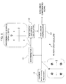
FIG. 9 is a diagram illustrating a signal input to the discriminator and a signal output from the discriminator on a complex plane (IQ plane) in the discrimination scheme 1-1; -
FIG. 10 is a diagram illustrating a relation between the signal input to the discriminator and the signal output from the discriminator on the IQ plane in the discrimination scheme 1-1; -
FIG. 11 is a block diagram illustrating an example of a configuration (discrimination scheme 1-2) of the discriminator illustrated inFIGS. 5 to 7 ; -
FIG. 12 is a flowchart for describing an example of operations of the discriminator illustrated inFIG. 11 ; -
FIG. 13 is a block diagram illustrating an example of a configuration (discrimination scheme 2) of the discriminator illustrated inFIGS. 5 to 7 ; -
FIG. 14 is a flowchart for describing an example of operations of the discriminator illustrated inFIG. 13 ; -
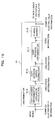
FIG. 15 is a block diagram illustrating an example of a configuration (discrimination scheme 3) of the discriminator illustrated inFIGS. 5 to 7 ; -
FIG. 16 is a flowchart for describing an example of operations of the discriminator illustrated inFIG. 15 ; -
FIG. 17 is a block diagram illustrating an example of a configuration (discrimination scheme 4) of the discriminator illustrated inFIGS. 5 to 7 ; -
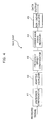
FIG. 18 is a flowchart for describing an example of operations of the discriminator illustrated inFIG. 17 ; -
FIG. 19 is a flowchart for describing an example of operations (discrimination scheme 5) of the discriminator illustrated inFIGS. 5 to 7 ; -
FIG. 20 is a diagram illustrating a signal input to the discriminator and a signal output from the discriminator on an IQ plane in thediscrimination scheme 5; -
FIG. 21 is a diagram illustrating a relation between the signal input to the discriminator and the signal output from the discriminator on the IQ plane in thediscrimination scheme 5; -
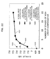
FIG. 22 is a diagram illustrating an example of a result of transmission simulation of non-linear equalization illustrated inFIGS. 4 to 21 ; -
FIG. 23 is a block diagram illustrating Modified Example 1 of the configuration illustrated inFIG. 4 ; -
FIG. 24 is a block diagram illustrating Modified Example 2 of the configuration illustrated inFIG. 4 ; and -
FIG. 25 is a block diagram illustrating Modified Example 3 of the configuration illustrated inFIG. 4 . - Hereinafter, embodiments will be described with reference to the drawings. However, the embodiments described below are merely examples and various modifications or applications of the technology not specified below are not intended to be excluded. Further, throughout the drawings used in the following embodiments, portions to which the same reference numerals are given indicate the same or equivalent portions unless otherwise stated.
-
FIG. 1 is a block diagram illustrating an example of an optical communication system according to an embodiment. Theoptical communication system 1 illustrated inFIG. 1 is, for example, a wavelength division multiplexing (WDM) optical transmission system which transmits WDM light. The WDMoptical transmission system 1 is configured to include, for example, a WDMoptical transmitter 10, anoptical transmission line 50 using an optical fiber, and a WDMoptical receiver 90. - The WDM
optical transmitter 10 transmits a WDM optical signal obtained by wavelength-multiplexing optical signals of multiple wavelengths (channels) to theoptical transmission line 50, and the WDMoptical receiver 90 demultiplexes the WDM optical signal transmitted through theoptical transmission line 50 into optical signals for each wavelength and receives the wavelength signals. The WDMoptical transmitter 10 and the WDMoptical receiver 90 are examples of communication apparatuses. - One or more of
optical amplifiers 30 or one or more ofrepeaters 70 may be provided for theoptical transmission line 50 according to a transmission distance of the WDM optical signal from the WDMoptical transmitter 10 to the WDMoptical receiver 90. - The WDM
optical transmitter 10 includes, for example, optical transmitters 11-1 to 11-N (where N is an integer equal to or greater than 2) provided for respective wavelengths and amultiplexer 12 that performs wavelength multiplexing (combining) on optical signals transmitted by the optical transmitters 11-1 to 11-N to generate a WDM optical signal and outputs the generated WDM optical signal. - Meanwhile, the WDM
optical receiver 90 includes, for example, ademultiplexer 91 that demultiplexes the WDM optical signal received from theoptical transmission line 50 into optical signals with the wavelengths and optical receivers 92-1 to 92-N that receives the optical signals with the respective wavelengths demultiplexed by thedemultiplexer 91. - Each of the optical transmitters 11-1 to 11-N may be an optical transmitter which transmits a single-polarized signal or may be an optical transmitter which transmits polarization multiplexed signals. An example of the configuration of the latter polarization multiplexed signal transmitter is illustrated in
FIG. 2 . The polarization multiplexed signal transmitter illustrated inFIG. 2 includes a digital signal processor (DSP) 111, a digital-analog converter (DAC) 112, a light source (laser diode, LD) 113, a beam splitter (BS) 114,IQ modulators - The
DSP 111 performs digital signal processing such as a non-linear pre-equalization described later on the transmission data signal. TheDSP 111 is an example of an arithmetic processing circuit, and the arithmetic processing circuit may be implemented by using a field programmable gate array (FPGA) or a large-scale integrated (LSI) circuit. - The
DAC 112 converts the transmission data signal processed as a digital signal by theDSP 111 into an analog signal and inputs the analog signal to theIQ modulators - The
light source 113 outputs transmission light, and theBS 114 splits the transmission light of thelight source 113 into two transmission lights to input the split lights to theIQ modulators - The
IQ modulators BS 114 according to the analog transmission data signal input from theDAC 112. One of theIQ modulators - The
PBC 116 performs polarization combination on the optical modulated signals of the polarized components from theIQ modulators - Meanwhile, as illustrated in
FIG. 3 , each of the optical receivers 92-1 to 92-N illustrated inFIG. 1 is configured to include, for example, a localoscillation light source 921, an opticalfront end 922, an analog-digital converter (ADC) 923, and aDSP 924. TheDSP 924 performs non-linear distortion compensation using virtual symbols. The opticalfront end 922 has a function of demodulating and photoelectrically-converting a received optical signal using local light of the localoscillation light source 921. TheADC 923 converts the reception analog electric signal photoelectrically-converted by the opticalfront end 922 into a digital signal and inputs the digital signal to theDSP 924. - The
DSP 924 performs signal processing including the non-linear distortion compensation using the above-mentioned virtual symbol on the reception digital electric signal input from theADC 923. TheDSP 924 is an example of an arithmetic processing circuit. Similarly to theDSP 111 of the transmission side, theDSP 924 may also be implemented by using an FPGA or an LSI circuit. - For example, as illustrated in
FIG. 4 , theDSP 924 may include, upon focusing on a functional configuration thereof, adispersion compensator 41, anadaptive equalizer 42, a frequency offsetcompensator 43, a carrierwave phase recovery 44, and anon-linear equalizer 45. As illustrated inFIG. 5 , thenon-linear equalizer 45 may include adiscriminator 61, anon-linear distortion calculator 62, and anon-linear compensator 63. Thenon-linear equalizer 45 may be disposed to the post stage of the carrierwave phase recovery 44, and one or more of other signal processors may be inserted before and after thenon-linear equalizer 45. Further, one or more of other signal processors may be interposed at any stages between theunits 41 to 44. Furthermore, one of theunits 41 to 43 may be unnecessary. - The
dispersion compensator 41 compensates, for example, wavelength dispersion occurred in the received signal (digital signal) by the digital signal processing. By performing compensation of the wavelength dispersion using the digital signal processing, an optical device such as a wavelength dispersion compensation fiber (DCF) may be unnecessary for the optical transmission line. Therefore, it is possible to obtain the advantages of suppressing an increase in optical noise occurred in compensation of DCF loss and suppressing wavelength distortion due to a non-linear optical effect in the DCF. Further, it is also possible to obtain the advantage of flexibly changing a dispersion compensation amount. When wavelength dispersion compensation is performed optically using the DCF or the like, thedispersion compensator 41 may be unnecessary. - The
adaptive equalizer 42 performs, for example, a polarization process including a separation of polarized components or a polarization mode dispersion (PMD) compensation (adaptive equalization) on the received signal (digital signal). The adaptive equalization is possible to compensate, by using a plurality of linear filters, polarization change and PMD waveform distortion according to time varying at a high speed by adaptively updating parameters of the linear filters at a sufficiently higher speed than that of the polarization change of the signal light in the optical fiber. - The frequency offset
compensator 43 compensates (or correct) a frequency offset between the received signal and the local oscillation light. For example, the frequency offsetcompensator 43 compensates a frequency offset by estimating a frequency offset from the received signal and applying reverse phase rotation corresponding to the estimated frequency offset to the received signal. The frequency offset estimation may be performed by using, for example, an estimation method called an exponentiation method or an estimation method called a predecision based angle differential frequency offset Estimator (PADE) method which is possible to extend an estimation range in comparison with the exponentiation method. - The carrier wave phase recovery (carrier phase estimator) 44 estimates and recovers a correct phase of the carrier by removing an amplified spontaneous emission (ASE) noise occurred in the
optical amplifier 30 or a laser phase noise from the received signal. The carrier phase estimation may be performed by using, for example, a feedback method which is possible to remove an effect of noise using a digital loop filter or a feed forward method which is possible to remove an effect of noise by averaging estimated phase differences detected by a phase detector. - The
non-linear equalizer 45 compensates (or equalizes) the non-linear distortion occurred in the received signal. For example, as illustrated inFIG. 5 , thenon-linear equalizer 45 is available to identify (or preliminarily discriminate) a symbol (QPSK symbol as a non-restrictive example) of the received signal, to calculate the non-linear distortion based on the preliminarily-discriminated symbol, and to compensate the non-linear distortion based on the result of the calculation. - For example, the
discriminator 61 discriminates the received signal with a specific symbol and outputs the discriminated symbol. Noise or the like in theoptical transmission line 50 is added to the received signal. As an example of a discrimination scheme of thediscriminator 61, there are schemes 1-1, 1-2, and 2 to 5 described later. - The
non-linear distortion calculator 62 calculates the non-linear distortion based on the symbol discriminated by thediscriminator 61. For example, thenon-linear distortion calculator 62 calculates the non-linear distortion occurred in every symbol due to the non-linear optical effect based on transmission line information, channel information, and the discriminated symbol. - As an example of the transmission line information, a transmission line length or a kind of optical fiber (a dispersion coefficient, an attenuation coefficient, a non-linear coefficient, or the like) can be exemplified. As an example of the channel information, a symbol rate, optical power input to an optical fiber, a central wavelength, or the like can be exemplified. For example, the transmission line information and the channel information can be stored in a memory (not illustrated) of the
DSP 924, and thenon-linear distortion calculator 62 appropriately reads information (parameters) used to calculate the non-linear distortion from the memory and calculates the non-linear distortion. The above-described perturbation analysis can be applied to the calculation. - The
non-linear compensator 63 performs the non-linear distortion compensation on the received signal based on the non-linear distortion calculated by thenon-linear distortion calculator 62. For example, thenon-linear compensator 63 subtracts the non-linear distortion calculated by thenon-linear distortion calculator 62 from the corresponding symbol of the received signal. - Although the QPSK signal is exemplified as a received signal in
FIG. 5 , the modulation scheme of the signal which can be compensated by thenon-linear equalizer 45 according to the embodiment is not limited to the QPSK signal. For example, thenon-linear equalizer 45 may compensate the non-linear distortion of the signal such as an amplitude-shift keying (ASK) signal, a phase-shift keying (PSK) signal, and a quadrature amplitude modulation (QAM) signal. As a non-restrictive example,FIG. 6 illustrates a state where a 16-QAM signal as a received signal is input to thenon-linear equalizer 45 and symbol identification (preliminary discrimination) is performed by thediscriminator 61. - Next,
FIG. 7 illustrates a flowchart for describing an example of operations of thenon-linear equalizer 45. As illustrated inFIG. 7 , first, the transmission line information and the channel information are stored in the memory of the DSP 924 (Process P11). - The input signal for the
non-linear equalizer 45 is split into two signals. One signal is input to thediscriminator 61, and the other signal is input to the non-linear compensator 63 (Process P12). - The input signal input to the
discriminator 61 is discriminated as a specific symbol by thediscriminator 61, and the discriminated symbol is input to the non-linear distortion calculator 62 (Process P13). - The
non-linear distortion calculator 62 appropriately reads out the aforementioned transmission line information and channel information from the memory, calculates the non-linear distortion occurred in every symbol based on the information and the symbol input from thediscriminator 61, and outputs a result of the calculation to the non-linear compensator 63 (Process P14). - The
non-linear compensator 63 compensates the non-linear distortion of every symbol by subtracting the non-linear distortion calculated by thenon-linear distortion calculator 62 from the corresponding symbol of the other split signal of the received signal (Process P15). - Next, the discrimination schemes 1-1, 1-2, and 2 to 5 performed by the
discriminator 61 will be described with reference toFIGS. 8 to 21 . - In the
discrimination scheme 1, as illustrated inFIG. 8 , first, a discriminated symbol (or arrangement) according to a modulation scheme for a main signal of a received signal is set in the discriminator 61 (Process P21). Next, thediscriminator 61 compares the set symbol (discrimination point) with the input main signal and outputs the symbol closest to the discrimination point on the IQ plane as a result of the discrimination (Processes P22 and P23). - As a non-restrictive example,
FIGS. 9 and10 illustrate a state where the received signal is a QPSK signal and the input signal is discriminated as any one of four discrimination points represented by 2 bits on the IQ plane in thediscriminator 61.FIG. 10 illustrates a state where an input symbol positioned on the first quadrant of the IQ plane is discriminated (or converted) and output as the discrimination point (QPSK symbol) set on the same first quadrant. - In the discrimination scheme 1-2, as illustrated in
FIG. 11 , thediscriminator 61 is configured to include ahard decision discriminator 611 and asymbol mapper 612. - The
hard decision discriminator 611 performs hard decision on a symbol (or complex electric field information) of the input main signal based on an error correction code given to the main signal on the transmission side (Processes P31 to P33 ofFIG. 12 ). For example, thehard decision discriminator 611 discriminates and converts the complex electric field information into code information (or binary data) in comparison with a threshold value. The complex electric field information is an example of signal information of the received optical signal. - The obtained code information is input to the
symbol mapper 612. Thesymbol mapper 612 performs re-mapping on the code information to a symbol (or complex electric field information) with the same scheme as that of the input main signal and outputs the symbol (Process P34 ofFIG. 12 ). For example, in the case where the input main signal is a QPSK signal, similarly to the cases ofFIGS. 9 and10 , the input main signal is re-mapped to any one of the four QPSK symbols represented by 2 bits on the IQ plane. - In the
discrimination scheme 2, as illustrated inFIG. 13 , thediscriminator 61 is configured to include thehard decision discriminator 611, a harddecision error corrector 613, and thesymbol mapper 612. - The
hard decision discriminator 611 performs hard decision on a symbol (or complex electric field information) of the input main signal based on an error correction code given to the main signal on the transmission side. For example, thehard decision discriminator 611 discriminates and converts the complex electric field information into code information (or binary data) in comparison with a threshold value. - The obtained code information is input to the hard decision error corrector 613 (Processes P41 to P43 of
FIG. 14 ). The harddecision error corrector 613 performs error correction on the input code information and inputs the error-corrected code information to the symbol mapper 612 (Process P44 ofFIG. 14 ). - The
symbol mapper 612 performs re-mapping on the error-corrected code information to a symbol (or complex electric field information) with the same scheme as that of the input main signal and outputs the symbol (Process P45 ofFIG. 14 ). For example, in the case where the input main signal is a QPSK signal, similarly toFIGS. 9 and10 , the input main signal is re-mapped to any one of the four QPSK symbols represented by 2 bits on the IQ plane. - In the
discrimination scheme 3, as illustrated inFIG. 15 , thediscriminator 61 is configured to include a soft decision discriminator (or likelihood calculator) 614, a softdecision error corrector 615, thehard decision discriminator 611, and thesymbol mapper 612. - The
soft decision discriminator 614 performs soft decision on a symbol (or complex electric field information) of the input main signal based on an error correction code given to the main signal on the transmission side. For example, thesoft decision discriminator 614 calculates likelihood information of the complex electric field information and inputs the likelihood information to the soft decision error corrector 615 (Processes P51 to P53 ofFIG. 16 ). - The soft
decision error corrector 615 performs error correction on the likelihood information input from thesoft decision discriminator 614 and inputs the error-corrected likelihood information to the hard decision discriminator 611 (Process P54 ofFIG. 16 ). Thehard decision discriminator 611 discriminates and converts the likelihood information into code information (or binary data) in comparison with a threshold value (Process P55 ofFIG. 16 ). - The obtained code information is input to the
symbol mapper 612. Thesymbol mapper 612 performs re-mapping on the code information to a symbol (or complex electric field information) with the same scheme as that of the input main signal and outputs the symbol (Process P56 ofFIG. 16 ). For example, in the case where the input main signal is a QPSK signal, similarly toFIGS. 9 and10 , the input main signal is re-mapped to any one of the four QPSK symbols represented by 2 bits on the IQ plane. - The discrimination scheme 4 corresponds to a combination of the above-described
discrimination scheme 2 including the hard decision and the above-describeddiscrimination scheme 3 including the soft decision. Therefore, as illustrated inFIG. 17 , thediscriminator 61 is configured to include the soft decision discriminator (or likelihood calculator) 614, the softdecision error corrector 615, thehard decision discriminator 611, the harddecision error corrector 613, and thesymbol mapper 612. - The
soft decision discriminator 614 performs soft decision on a symbol (or complex electric field information) of the input main signal based on an error correction code given to the main signal on the transmission side. For example, thesoft decision discriminator 614 calculates likelihood information of the complex electric field information and inputs the likelihood information to the soft decision error corrector 615 (Processes P61 to P63 ofFIG. 18 ). - The soft
decision error corrector 615 performs error correction on the likelihood information input from thesoft decision discriminator 614 and inputs the error-corrected likelihood information to the hard decision discriminator 611 (Process P64 ofFIG. 18 ). Thehard decision discriminator 611 discriminates and converts the likelihood information into code information (binary data) in comparison with a threshold value (Process P65 ofFIG. 18 ). - The obtained code information is input to the hard
decision error corrector 613. The harddecision error corrector 613 performs error correction on the input code information and inputs the error-corrected code information to the symbol mapper 612 (Process P66 ofFIG. 18 ). - The
symbol mapper 612 performs re-mapping on the error-corrected code information to a symbol (or complex electric field information) with the same scheme as that of the input main signal and outputs the symbol (Process P67 ofFIG. 18 ). For example, in the case where the input main signal is a QPSK signal, similarly toFIGS. 9 and10 , the input main signal is re-mapped to any one of the four QPSK symbols represented by 2 bits on the IQ plane. - In the
discrimination scheme 5, an arbitrary symbol (at least one symbol) on the IQ plane may be set as a discriminated symbol in the discriminator 61 (Process P71 ofFIG. 19 ). Thediscriminator 61 outputs a symbol corresponding to the set symbol of which a distance from the data of the input main signal on the IQ plane is minimum as complex electric field information (Processes P72 and P73 ofFIG. 19 ). - Herein, for example, as illustrated in
FIGS. 20 and21 , the calculation of the following stages can be simplified by setting four symbols (symbols of which a multivalued level is lower than that of the main signal) such as QPSK symbols as discriminated symbols in the 16-QAM modulated main signal. - Next,
FIG. 22 illustrates an example of a confirmatory result of the non-linear compensation effect obtained through transmission simulation by the above-describednon-linear equalizer 45. In the transmission simulation, the transmission where a dual polarization (DP)-QPSK signal with 127 Gbits/second is 11-wavelength multiplexed at a 50GHz frequency interval was simulated. Herein, the input power of the optical transmission line (or optical fiber) is set to 3 dBm/channel; the OSNR is set to 14 dB; and the length of transmission line is set to 100 km of single mode fiber x 25 spans = 2500 km. - In
FIG. 22 , the horizontal axis denotes the number of stages of a non-linear compensator, and the vertical axis denotes a Q-factor corresponding to a reception bit error rate. In addition, inFIG. 22 ,reference numeral 300 indicates a Q-factor of the case where no non-linear compensation is provided (the number of stages = 0);reference numeral 400 indicates a Q-factor of the case where one stage to twenty stages of non-linear compensators of the related art are provided; andreference numeral 600 indicates a Q-factor of the case where one stage of the above-describednon-linear equalizer 45 is provided. Herein, the "non-linear compensators of the related art" correspond to, for example, a non-linear compensator configured as multiple stages by alternately combining a dispersion compensator and a non-linear compensator in thedispersion compensator 41 disposed to the front stage of the carrierwave phase recovery 44 illustrated inFIG. 4 . In addition, inFIG. 22 ,reference numeral 500 indicates a Q-factor of the case where the non-linear compensation is performed on the transmission side instead of the reception side (i.e., the case of non-linear pre-equalization). - As understood from
FIG. 22 , according to the non-linear compensation by thenon-linear equalizer 45 according to the embodiment, a single stage of thenon-linear equalizer 45 can achieve the same effect of improvement of the Q-factor of the case where the three stages of the non-linear compensators of the related art are provided. In addition, it can be understood that the non-linear pre-equalization (refer to reference numeral 500) of the transmission side can achieve the same effect (Q-factor) as that of the case where five stages of non-linear compensators of the related art are provided in the reception side, and if thenon-linear equalizer 45 is provided in the post stage of the carrierwave phase recovery 44, the effect is slightly deteriorated. This is because the non-linear distortion is calculated based on the received signal including a code error. However, it is confirmed that the degree of deterioration is about 0.1 dB. - In the above-described example, although the
discriminator 61 is provided in thenon-linear equalizer 45, thediscriminator 61 may be unnecessary. In this case, thenon-linear distortion calculator 62 can calculate the non-linear distortion based on the signal information of the received optical signal by using perturbation analysis. However, thediscriminator 61 may be provided to discriminate the signal information as a specific symbol as described before, so that the calculation of the non-linear distortion can be simplified. -
FIG. 23 is a block diagram illustrating Modified Example 1 of a functional configuration of theDSP 924 illustrated inFIG. 4 . In the configuration illustrated inFIG. 23 , another carrierwave phase recovery 46 is provided in the post stage of thenon-linear equalizer 45 which is provided in the post stage of the carrierwave phase recovery 44. Theother signal processor 40 illustrated inFIG. 23 may include any one of thedispersion compensator 41, theadaptive equalizer 42, and the frequency offsetcompensator 43 illustrated inFIG. 4 . - The carrier
wave phase recovery 46 performs carrier wave phase recovery on the received signal of which non-linearity is equalized (or compensated) by thenon-linear equalizer 45, so that it is possible to improve accuracy of the carrier wave phase recovery in comparison with the configuration illustrated inFIG. 4 . - The algorithms of the carrier wave phase recovery used by in two carrier
wave phase recoveries wave phase recoveries wave phase recovery 46 may be set to be larger than that in the front carrierwave phase recovery 44. According to this setting, coarse carrier wave phase recovery can be performed at a high rate in the front carrierwave phase recovery 44, and then, fine (or highly accurate) carrier wave phase recovery can be performed in the post carrierwave phase recovery 46. - As illustrated in
FIG. 24 , N (N is an integer of 2 or more) sets of thenon-linear equalizer 45 and the post carrierwave phase recovery 46 illustrated in Modified Example 1 may be provided. In this case, the non-linear equalization and the carrier wave phase recovery are repetitively performed N times, so that it is possible to further improve the accuracy of the carrier wave phase recovery in comparison with Modified Example 1. - The above-described
non-linear equalizer 45 may be used together with another non-linear compensator (or a non-linear equalizer) may be used.FIG. 25 illustrates an example of a combination of thenon-linear equalizer 45 according to the embodiment and anon-linear compensator 41a using a backward propagation method. Thenon-linear compensator 41a is provided, for example, in the front stage of the carrier wave phase recovery 44 (for example, in the front stage of the adaptive equalizer 42) to compensate the non-linear distortion occurred in the received signal due to the non-linear optical effect. Since the non-linear compensation is performed before and after the carrier wave phase recovery, it is possible to improve a compensation performance of the non-linear distortion. - In addition, as illustrated in
FIG. 25 , M (M is an integer of M ≥ 1) stages of a set of thenon-linear compensator 41a and thedispersion compensator 41 may be provided. In this case, since the dispersion compensation and the non-linear compensation are alternately performed on the received signal M times, it is possible to improve a compensation performance of the wavelength dispersion and the non-linear distortion. Other signal processors may be provided in any stages between theblocks FIG. 25 .
Claims (10)
- A non-linear distortion compensator comprising:a non-linear distortion calculator (62) configured to calculate non-linear distortion occurred in a received optical signal based on signal information after recovery of a carrier wave in a carrier wave phase recovery (44) being configured to recover a phase of the carrier wave of the received optical signal; anda non-linear compensator (63) configured to compensate the non-linear distortion of the received optical signal based on the non-linear distortion obtained by the non-linear distortion calculator (62).
- The non-linear distortion compensator according to claim 1,
wherein the received optical signal is a phase modulation signal or a quadrature amplitude modulation signal, and
wherein the non-linear distortion compensation apparatus further comprises a discriminator (61) configured to discriminate the signal information as a specific symbol according to the modulation and input a result of the discrimination to the non-linear distortion calculator. - The non-linear distortion compensator according to claim 2, wherein the discriminator (61) comprises:a hard decision discriminator (611) configured to perform hard decision on the signal information; anda symbol mapper (612) configured to map a hard decision result obtained by the hard decision discriminator (611) to the specific symbol.
- The non-linear distortion compensator according to claim 2,
wherein the received optical signal is a signal with an error correction code, and
wherein the discriminator (61) includes:a hard decision discriminator (611) configured to perform hard decision on the signal information;a hard decision error corrector (613) configured to perform error correction on a hard decision result obtained by the hard decision discriminator based on the error correction code; anda symbol mapper (612) configured to map an error correction result obtained by the hard decision error corrector (613) to the specific symbol. - The non-linear distortion compensator according to claim 2,
wherein the received optical signal is a signal with an error correction code, and
wherein the discriminator (61) comprises:a soft decision discriminator (614) configured to perform soft decision on the signal information;a soft decision error corrector (615) configured to perform error correction on a soft decision result obtained by the soft decision discriminator (614) based on the error correction code; anda symbol mapper (612) configured to map an error correction result obtained by the soft decision error corrector (615) to the specific symbol. - The non-linear distortion compensator according to claim 2,
wherein the received optical signal is a signal with an error correction code, and
wherein the discriminator (61) comprises:a soft decision discriminator (614) configured to perform soft decision on the signal information;a soft decision error corrector (615) configured to perform error correction on a soft decision result obtained by the soft decision discriminator (614) based on the error correction code;a hard decision discriminator (611) configured to perform hard decision on an error correction result obtained by the soft decision error corrector (615);a hard decision error corrector (613) configured to perform error correction on a hard decision result obtained by the hard decision discriminator (611) based on the error correction code; anda symbol mapper (612) configured to map an error correction result obtained by the hard decision corrector (613) to the specific symbol. - The non-linear distortion compensator according to claim 2,
wherein the discriminator (61) configured to output a symbol as the result of the discrimination, the symbol being at least one of symbols set on a complex plane as a discriminated symbol and a distance from the input signal information on the complex plane being in minimum. - The non-linear distortion compensator according to claim 7,
wherein a multivalued level of the symbol set on the complex plane is lower than that of the received optical signal. - A method of compensating non-linear distortion, the method comprising:recovering a phase of a carrier wave of a received optical signal;calculating non-linear distortion occurred in the received optical signal based on signal information after the recovery of the carrier wave; andcompensating the non-linear distortion of the received optical signal based on the non-linear distortion obtained by the calculation.
- An optical receiver comprising:a carrier wave phase recovery (44) configured to recover a phase of a carrier wave of a received optical signal; andthe non-linear distortion compensation apparatus (45) according to any one of claims 1 to 8.
Applications Claiming Priority (1)
| Application Number | Priority Date | Filing Date | Title |
|---|---|---|---|
| JP2013188671A JP6135415B2 (en) | 2013-09-11 | 2013-09-11 | Nonlinear distortion compensation apparatus and method, and optical receiver |
Publications (2)
| Publication Number | Publication Date |
|---|---|
| EP2858272A1 true EP2858272A1 (en) | 2015-04-08 |
| EP2858272B1 EP2858272B1 (en) | 2018-09-12 |
Family
ID=51392122
Family Applications (1)
| Application Number | Title | Priority Date | Filing Date |
|---|---|---|---|
| EP14182091.0A Not-in-force EP2858272B1 (en) | 2013-09-11 | 2014-08-25 | Non-linear distortion compensator, method of compensating non-linear distortion, and optical receiver |
Country Status (3)
| Country | Link |
|---|---|
| US (1) | US9363014B2 (en) |
| EP (1) | EP2858272B1 (en) |
| JP (1) | JP6135415B2 (en) |
Cited By (1)
| Publication number | Priority date | Publication date | Assignee | Title |
|---|---|---|---|---|
| EP4407895A1 (en) * | 2023-01-26 | 2024-07-31 | Nokia Solutions and Networks Oy | Perturbation-based hard-decision nonlinearity compensation |
Families Citing this family (13)
| Publication number | Priority date | Publication date | Assignee | Title |
|---|---|---|---|---|
| EP2804334A1 (en) * | 2013-05-13 | 2014-11-19 | Xieon Networks S.à.r.l. | Method, device and communication system for reducing optical transmission impairments |
| JP6176012B2 (en) * | 2013-09-11 | 2017-08-09 | 富士通株式会社 | Nonlinear distortion compensation apparatus and method, and communication apparatus |
| JP6135415B2 (en) * | 2013-09-11 | 2017-05-31 | 富士通株式会社 | Nonlinear distortion compensation apparatus and method, and optical receiver |
| CN104980379B (en) * | 2014-04-11 | 2018-06-08 | 富士通株式会社 | Estimation device, method and the receiver of non-linear distortion |
| US9941963B2 (en) * | 2014-05-12 | 2018-04-10 | Telefonaktiebolaget Lm Ericsson (Publ) | Non-linear propagation impairment equalization |
| US9673911B2 (en) * | 2014-05-13 | 2017-06-06 | Infinera Corporation | Tracking nonlinear cross-phase modulation noise and linewidth induced jitter in coherent optical fiber communication links |
| US9231787B1 (en) * | 2015-01-23 | 2016-01-05 | Huawei Technologies Co., Ltd. | Method and apparatus with improved estimation accuracy and robustness for fine frequency offset estimation in coherent receivers |
| US9906309B2 (en) * | 2015-03-31 | 2018-02-27 | Infinera Corporation | System and method for determining nonlinear mitigation perturbative distortion coefficients using a received optical signal |
| US10236982B1 (en) * | 2017-12-21 | 2019-03-19 | Ciena Corporation | Fiber parameter identification |
| US10389473B1 (en) * | 2018-04-27 | 2019-08-20 | Fujitsu Limited | Reach extension for optical networks through control of modulation formats and numbers of subcarriers |
| CN113938199B (en) | 2020-06-29 | 2025-06-03 | 中兴通讯股份有限公司 | Signal processing method and device, storage medium, and electronic device |
| EP4099584B1 (en) * | 2021-06-01 | 2024-04-03 | Nokia Solutions and Networks Oy | Mitigation of equalization-enhanced phase noise in a coherent optical receiver |
| CN116363035A (en) * | 2022-12-14 | 2023-06-30 | 广西大学 | A method and system for nonlinear carrier phase removal of fringe projection images |
Citations (7)
| Publication number | Priority date | Publication date | Assignee | Title |
|---|---|---|---|---|
| JP2008211493A (en) | 2007-02-26 | 2008-09-11 | Mitsubishi Electric Corp | Distributed pre-equalization optical communication system |
| EP2071747A1 (en) * | 2006-09-26 | 2009-06-17 | Hitachi Communication Technologies, Ltd. | Optical electric field receiver and optical transmission system |
| JP2009278613A (en) | 2008-03-20 | 2009-11-26 | Toshiba Corp | Wireless communication device |
| WO2012006575A1 (en) * | 2010-07-09 | 2012-01-12 | Huawei Technologies Co., Ltd. | Method and apparatus for carrier phase estimation and correction in a coherent optical system |
| JP2012075097A (en) | 2010-09-28 | 2012-04-12 | Fujitsu Ltd | Nonlinear compensation device, and transmitter |
| US20120128377A1 (en) * | 2010-11-22 | 2012-05-24 | Fujitsu Limited | Optical digital coherent receiver |
| JP2012120010A (en) | 2010-12-02 | 2012-06-21 | Fujitsu Ltd | Optical transmitter and optical transmission device |
Family Cites Families (20)
| Publication number | Priority date | Publication date | Assignee | Title |
|---|---|---|---|---|
| US6985549B1 (en) * | 2000-10-20 | 2006-01-10 | Ati Research, Inc. | Blind cost criterion timing recovery |
| US7398454B2 (en) * | 2004-12-21 | 2008-07-08 | Tyco Telecommunications (Us) Inc. | System and method for forward error correction decoding using soft information |
| US7606498B1 (en) * | 2005-10-21 | 2009-10-20 | Nortel Networks Limited | Carrier recovery in a coherent optical receiver |
| US8923419B2 (en) * | 2006-02-27 | 2014-12-30 | Cohda Wireless Pty. Ltd. | Method and system for communication in a wireless network |
| CN101589556A (en) * | 2006-10-05 | 2009-11-25 | 新加坡科技研究局 | Method and system and computer program product for estimating a signal |
| JP5340004B2 (en) * | 2008-06-18 | 2013-11-13 | 株式会社日立製作所 | Balance compensation type optical balanced receiver and optical IQ receiver |
| US20090322961A1 (en) * | 2008-06-27 | 2009-12-31 | Limberg Allen Leroy | System for digital television broadcasting using modified 2/3 trellis coding |
| US20090324224A1 (en) | 2008-06-30 | 2009-12-31 | Chongjin Xie | System, method and apparatus to suppress inter-channel nonlinearities in WDM systems with coherent detection |
| ATE488920T1 (en) * | 2008-07-16 | 2010-12-15 | Alcatel Lucent | ADAPTIVE NONLINEARITY COMPENSATION IN A COHERENT RECEIVER |
| CN102318306A (en) * | 2009-03-02 | 2012-01-11 | 株式会社日立制作所 | optical multi-value transmission system |
| KR101287753B1 (en) * | 2009-03-26 | 2013-07-19 | 후지쯔 가부시끼가이샤 | Multi-antenna communication device and multi-antenna communication method |
| JP5419534B2 (en) * | 2009-05-11 | 2014-02-19 | 三菱電機株式会社 | FEC frame construction apparatus and method |
| JP5375519B2 (en) * | 2009-10-26 | 2013-12-25 | 富士通株式会社 | Nonlinear distortion detection circuit, optical receiver, optical transmission system, and nonlinear distortion detection method |
| DE102010051710B4 (en) * | 2010-07-21 | 2013-03-14 | Power Plus Communications Ag | Method for assessing the usability of a subcarrier of a broadband powerline signal |
| US9203682B2 (en) * | 2010-09-07 | 2015-12-01 | Alcatel Lucent | Frequency-dependent I/Q-signal imbalance correction coherent optical transceivers |
| JP5671071B2 (en) * | 2011-02-07 | 2015-02-18 | 日本電信電話株式会社 | Digital signal processor |
| CN103095374B (en) | 2011-10-28 | 2016-04-20 | 富士通株式会社 | The method and apparatus of the self-adaptation nonlinear equilibrium of palarization multiplexing optical communication system |
| EP2651051A1 (en) | 2012-04-13 | 2013-10-16 | Alcatel Lucent | Nonlinear Cross-Polarization Mitigation Algorithm |
| US9319137B2 (en) | 2013-09-09 | 2016-04-19 | Ciena Corporation | Methods and systems for reduced complexity nonlinear compensation |
| JP6135415B2 (en) * | 2013-09-11 | 2017-05-31 | 富士通株式会社 | Nonlinear distortion compensation apparatus and method, and optical receiver |
-
2013
- 2013-09-11 JP JP2013188671A patent/JP6135415B2/en not_active Expired - Fee Related
-
2014
- 2014-08-15 US US14/461,167 patent/US9363014B2/en not_active Expired - Fee Related
- 2014-08-25 EP EP14182091.0A patent/EP2858272B1/en not_active Not-in-force
Patent Citations (7)
| Publication number | Priority date | Publication date | Assignee | Title |
|---|---|---|---|---|
| EP2071747A1 (en) * | 2006-09-26 | 2009-06-17 | Hitachi Communication Technologies, Ltd. | Optical electric field receiver and optical transmission system |
| JP2008211493A (en) | 2007-02-26 | 2008-09-11 | Mitsubishi Electric Corp | Distributed pre-equalization optical communication system |
| JP2009278613A (en) | 2008-03-20 | 2009-11-26 | Toshiba Corp | Wireless communication device |
| WO2012006575A1 (en) * | 2010-07-09 | 2012-01-12 | Huawei Technologies Co., Ltd. | Method and apparatus for carrier phase estimation and correction in a coherent optical system |
| JP2012075097A (en) | 2010-09-28 | 2012-04-12 | Fujitsu Ltd | Nonlinear compensation device, and transmitter |
| US20120128377A1 (en) * | 2010-11-22 | 2012-05-24 | Fujitsu Limited | Optical digital coherent receiver |
| JP2012120010A (en) | 2010-12-02 | 2012-06-21 | Fujitsu Ltd | Optical transmitter and optical transmission device |
Non-Patent Citations (1)
| Title |
|---|
| KHAIRUZZAMAN ET AL: "Equalization of nonlinear transmission impairments by maximum-likelihood-sequence estimation in digital coherent receivers", OPTICS EXPRESS, vol. 18, no. 5, 1 March 2010 (2010-03-01), pages 4776 - 4782, XP002736345 * |
Cited By (1)
| Publication number | Priority date | Publication date | Assignee | Title |
|---|---|---|---|---|
| EP4407895A1 (en) * | 2023-01-26 | 2024-07-31 | Nokia Solutions and Networks Oy | Perturbation-based hard-decision nonlinearity compensation |
Also Published As
| Publication number | Publication date |
|---|---|
| US20150071630A1 (en) | 2015-03-12 |
| JP2015056753A (en) | 2015-03-23 |
| JP6135415B2 (en) | 2017-05-31 |
| US9363014B2 (en) | 2016-06-07 |
| EP2858272B1 (en) | 2018-09-12 |
Similar Documents
| Publication | Publication Date | Title |
|---|---|---|
| EP2858272B1 (en) | Non-linear distortion compensator, method of compensating non-linear distortion, and optical receiver | |
| EP2852076B1 (en) | Non-linear distortion compensator, method of compensating non-linear distortion, and communication apparatus | |
| JP6485095B2 (en) | Optical transmission device, optical transmission system, and polarization dependent loss monitor | |
| EP3176964B1 (en) | Coherent communication system, communication method, and transmission method | |
| Liu et al. | Digital signal processing techniques enabling multi-Tb\/s superchannel transmission: an overview of recent advances in DSP-enabled superchannels | |
| JP4620642B2 (en) | Multilevel modulation receiver | |
| US9225455B2 (en) | Digital non-linear compensation in optical communication systems | |
| US10594406B2 (en) | Pilot-aided digital signal processing for reception of coherent optical communication | |
| EP2924890A1 (en) | Polarization state detector, optical transmitter, and optical receiver | |
| US20160056889A1 (en) | Optical spatial-division multiplexed transmission system and transmission method | |
| Do et al. | Data-aided OSNR estimation for QPSK and 16-QAM coherent optical system | |
| US9634764B2 (en) | Estimating device and method for estimating | |
| US9692521B1 (en) | Polarization pre-compensation technique for polarization-division-multiplexed direct-detection optical communication systems | |
| WO2016145493A1 (en) | Method and system for polarisation division multiplexed optical transmission | |
| Asif et al. | Logarithmic step-size based digital backward propagation in N-channel 112Gbit/s/ch DP-QPSK transmission | |
| JP6211202B2 (en) | Optical transmission method and optical transmission system | |
| Lin | Digital nonlinear compensation for next-generation optical communication systems using advanced modulation formats | |
| Ranzini et al. | Impact of nonlinear effects and mitigation on coherent optical systems | |
| Okamoto et al. | Digital in-band OSNR estimation for polarization-multiplexed optical transmission | |
| Goroshko et al. | Fundamental limitations of digital back propagation due to polarization mode dispersion | |
| Ranzini et al. | Accurate blind chromatic dispersion estimation in long-haul 112Gbit/s PM-QPSK WDM Coherent Systems | |
| Meng et al. | Long-haul 112 Gbit/s coherent polarization multiplexing QPSK transmission experiment on G. 652 fiber with the improved DSP unit | |
| Simões et al. | Impact of Special Fibers on the Number of Optical Repeaters in Submarine Systems | |
| Kikuchi | Digital coherent transmission | |
| Yaman et al. | Interchannel nonlinear impairment compensation by advanced split-step method |
Legal Events
| Date | Code | Title | Description |
|---|---|---|---|
| PUAI | Public reference made under article 153(3) epc to a published international application that has entered the european phase |
Free format text: ORIGINAL CODE: 0009012 |
|
| 17P | Request for examination filed |
Effective date: 20140825 |
|
| AK | Designated contracting states |
Kind code of ref document: A1 Designated state(s): AL AT BE BG CH CY CZ DE DK EE ES FI FR GB GR HR HU IE IS IT LI LT LU LV MC MK MT NL NO PL PT RO RS SE SI SK SM TR |
|
| AX | Request for extension of the european patent |
Extension state: BA ME |
|
| R17P | Request for examination filed (corrected) |
Effective date: 20150928 |
|
| RBV | Designated contracting states (corrected) |
Designated state(s): AL AT BE BG CH CY CZ DE DK EE ES FI FR GB GR HR HU IE IS IT LI LT LU LV MC MK MT NL NO PL PT RO RS SE SI SK SM TR |
|
| GRAP | Despatch of communication of intention to grant a patent |
Free format text: ORIGINAL CODE: EPIDOSNIGR1 |
|
| STAA | Information on the status of an ep patent application or granted ep patent |
Free format text: STATUS: GRANT OF PATENT IS INTENDED |
|
| INTG | Intention to grant announced |
Effective date: 20180326 |
|
| GRAS | Grant fee paid |
Free format text: ORIGINAL CODE: EPIDOSNIGR3 |
|
| GRAA | (expected) grant |
Free format text: ORIGINAL CODE: 0009210 |
|
| STAA | Information on the status of an ep patent application or granted ep patent |
Free format text: STATUS: THE PATENT HAS BEEN GRANTED |
|
| AK | Designated contracting states |
Kind code of ref document: B1 Designated state(s): AL AT BE BG CH CY CZ DE DK EE ES FI FR GB GR HR HU IE IS IT LI LT LU LV MC MK MT NL NO PL PT RO RS SE SI SK SM TR |
|
| REG | Reference to a national code |
Ref country code: GB Ref legal event code: FG4D |
|
| REG | Reference to a national code |
Ref country code: CH Ref legal event code: EP |
|
| REG | Reference to a national code |
Ref country code: IE Ref legal event code: FG4D |
|
| REG | Reference to a national code |
Ref country code: DE Ref legal event code: R096 Ref document number: 602014032158 Country of ref document: DE |
|
| REG | Reference to a national code |
Ref country code: AT Ref legal event code: REF Ref document number: 1041831 Country of ref document: AT Kind code of ref document: T Effective date: 20181015 |
|
| REG | Reference to a national code |
Ref country code: NL Ref legal event code: MP Effective date: 20180912 |
|
| REG | Reference to a national code |
Ref country code: LT Ref legal event code: MG4D |
|
| PG25 | Lapsed in a contracting state [announced via postgrant information from national office to epo] |
Ref country code: FI Free format text: LAPSE BECAUSE OF FAILURE TO SUBMIT A TRANSLATION OF THE DESCRIPTION OR TO PAY THE FEE WITHIN THE PRESCRIBED TIME-LIMIT Effective date: 20180912 Ref country code: LT Free format text: LAPSE BECAUSE OF FAILURE TO SUBMIT A TRANSLATION OF THE DESCRIPTION OR TO PAY THE FEE WITHIN THE PRESCRIBED TIME-LIMIT Effective date: 20180912 Ref country code: BG Free format text: LAPSE BECAUSE OF FAILURE TO SUBMIT A TRANSLATION OF THE DESCRIPTION OR TO PAY THE FEE WITHIN THE PRESCRIBED TIME-LIMIT Effective date: 20181212 Ref country code: GR Free format text: LAPSE BECAUSE OF FAILURE TO SUBMIT A TRANSLATION OF THE DESCRIPTION OR TO PAY THE FEE WITHIN THE PRESCRIBED TIME-LIMIT Effective date: 20181213 Ref country code: NO Free format text: LAPSE BECAUSE OF FAILURE TO SUBMIT A TRANSLATION OF THE DESCRIPTION OR TO PAY THE FEE WITHIN THE PRESCRIBED TIME-LIMIT Effective date: 20181212 Ref country code: RS Free format text: LAPSE BECAUSE OF FAILURE TO SUBMIT A TRANSLATION OF THE DESCRIPTION OR TO PAY THE FEE WITHIN THE PRESCRIBED TIME-LIMIT Effective date: 20180912 Ref country code: SE Free format text: LAPSE BECAUSE OF FAILURE TO SUBMIT A TRANSLATION OF THE DESCRIPTION OR TO PAY THE FEE WITHIN THE PRESCRIBED TIME-LIMIT Effective date: 20180912 |
|
| PG25 | Lapsed in a contracting state [announced via postgrant information from national office to epo] |
Ref country code: LV Free format text: LAPSE BECAUSE OF FAILURE TO SUBMIT A TRANSLATION OF THE DESCRIPTION OR TO PAY THE FEE WITHIN THE PRESCRIBED TIME-LIMIT Effective date: 20180912 Ref country code: AL Free format text: LAPSE BECAUSE OF FAILURE TO SUBMIT A TRANSLATION OF THE DESCRIPTION OR TO PAY THE FEE WITHIN THE PRESCRIBED TIME-LIMIT Effective date: 20180912 Ref country code: HR Free format text: LAPSE BECAUSE OF FAILURE TO SUBMIT A TRANSLATION OF THE DESCRIPTION OR TO PAY THE FEE WITHIN THE PRESCRIBED TIME-LIMIT Effective date: 20180912 |
|
| REG | Reference to a national code |
Ref country code: AT Ref legal event code: MK05 Ref document number: 1041831 Country of ref document: AT Kind code of ref document: T Effective date: 20180912 |
|
| PG25 | Lapsed in a contracting state [announced via postgrant information from national office to epo] |
Ref country code: IS Free format text: LAPSE BECAUSE OF FAILURE TO SUBMIT A TRANSLATION OF THE DESCRIPTION OR TO PAY THE FEE WITHIN THE PRESCRIBED TIME-LIMIT Effective date: 20190112 Ref country code: AT Free format text: LAPSE BECAUSE OF FAILURE TO SUBMIT A TRANSLATION OF THE DESCRIPTION OR TO PAY THE FEE WITHIN THE PRESCRIBED TIME-LIMIT Effective date: 20180912 Ref country code: IT Free format text: LAPSE BECAUSE OF FAILURE TO SUBMIT A TRANSLATION OF THE DESCRIPTION OR TO PAY THE FEE WITHIN THE PRESCRIBED TIME-LIMIT Effective date: 20180912 Ref country code: PL Free format text: LAPSE BECAUSE OF FAILURE TO SUBMIT A TRANSLATION OF THE DESCRIPTION OR TO PAY THE FEE WITHIN THE PRESCRIBED TIME-LIMIT Effective date: 20180912 Ref country code: EE Free format text: LAPSE BECAUSE OF FAILURE TO SUBMIT A TRANSLATION OF THE DESCRIPTION OR TO PAY THE FEE WITHIN THE PRESCRIBED TIME-LIMIT Effective date: 20180912 Ref country code: NL Free format text: LAPSE BECAUSE OF FAILURE TO SUBMIT A TRANSLATION OF THE DESCRIPTION OR TO PAY THE FEE WITHIN THE PRESCRIBED TIME-LIMIT Effective date: 20180912 Ref country code: RO Free format text: LAPSE BECAUSE OF FAILURE TO SUBMIT A TRANSLATION OF THE DESCRIPTION OR TO PAY THE FEE WITHIN THE PRESCRIBED TIME-LIMIT Effective date: 20180912 Ref country code: ES Free format text: LAPSE BECAUSE OF FAILURE TO SUBMIT A TRANSLATION OF THE DESCRIPTION OR TO PAY THE FEE WITHIN THE PRESCRIBED TIME-LIMIT Effective date: 20180912 Ref country code: CZ Free format text: LAPSE BECAUSE OF FAILURE TO SUBMIT A TRANSLATION OF THE DESCRIPTION OR TO PAY THE FEE WITHIN THE PRESCRIBED TIME-LIMIT Effective date: 20180912 |
|
| PG25 | Lapsed in a contracting state [announced via postgrant information from national office to epo] |
Ref country code: SM Free format text: LAPSE BECAUSE OF FAILURE TO SUBMIT A TRANSLATION OF THE DESCRIPTION OR TO PAY THE FEE WITHIN THE PRESCRIBED TIME-LIMIT Effective date: 20180912 Ref country code: PT Free format text: LAPSE BECAUSE OF FAILURE TO SUBMIT A TRANSLATION OF THE DESCRIPTION OR TO PAY THE FEE WITHIN THE PRESCRIBED TIME-LIMIT Effective date: 20190112 Ref country code: SK Free format text: LAPSE BECAUSE OF FAILURE TO SUBMIT A TRANSLATION OF THE DESCRIPTION OR TO PAY THE FEE WITHIN THE PRESCRIBED TIME-LIMIT Effective date: 20180912 |
|
| REG | Reference to a national code |
Ref country code: DE Ref legal event code: R097 Ref document number: 602014032158 Country of ref document: DE |
|
| PLBE | No opposition filed within time limit |
Free format text: ORIGINAL CODE: 0009261 |
|
| STAA | Information on the status of an ep patent application or granted ep patent |
Free format text: STATUS: NO OPPOSITION FILED WITHIN TIME LIMIT |
|
| PG25 | Lapsed in a contracting state [announced via postgrant information from national office to epo] |
Ref country code: DK Free format text: LAPSE BECAUSE OF FAILURE TO SUBMIT A TRANSLATION OF THE DESCRIPTION OR TO PAY THE FEE WITHIN THE PRESCRIBED TIME-LIMIT Effective date: 20180912 |
|
| 26N | No opposition filed |
Effective date: 20190613 |
|
| PG25 | Lapsed in a contracting state [announced via postgrant information from national office to epo] |
Ref country code: SI Free format text: LAPSE BECAUSE OF FAILURE TO SUBMIT A TRANSLATION OF THE DESCRIPTION OR TO PAY THE FEE WITHIN THE PRESCRIBED TIME-LIMIT Effective date: 20180912 |
|
| PG25 | Lapsed in a contracting state [announced via postgrant information from national office to epo] |
Ref country code: TR Free format text: LAPSE BECAUSE OF FAILURE TO SUBMIT A TRANSLATION OF THE DESCRIPTION OR TO PAY THE FEE WITHIN THE PRESCRIBED TIME-LIMIT Effective date: 20180912 |
|
| PG25 | Lapsed in a contracting state [announced via postgrant information from national office to epo] |
Ref country code: CH Free format text: LAPSE BECAUSE OF NON-PAYMENT OF DUE FEES Effective date: 20190831 Ref country code: LU Free format text: LAPSE BECAUSE OF NON-PAYMENT OF DUE FEES Effective date: 20190825 Ref country code: LI Free format text: LAPSE BECAUSE OF NON-PAYMENT OF DUE FEES Effective date: 20190831 Ref country code: MC Free format text: LAPSE BECAUSE OF FAILURE TO SUBMIT A TRANSLATION OF THE DESCRIPTION OR TO PAY THE FEE WITHIN THE PRESCRIBED TIME-LIMIT Effective date: 20180912 |
|
| REG | Reference to a national code |
Ref country code: BE Ref legal event code: MM Effective date: 20190831 |
|
| PG25 | Lapsed in a contracting state [announced via postgrant information from national office to epo] |
Ref country code: IE Free format text: LAPSE BECAUSE OF NON-PAYMENT OF DUE FEES Effective date: 20190825 |
|
| PG25 | Lapsed in a contracting state [announced via postgrant information from national office to epo] |
Ref country code: BE Free format text: LAPSE BECAUSE OF NON-PAYMENT OF DUE FEES Effective date: 20190831 |
|
| PG25 | Lapsed in a contracting state [announced via postgrant information from national office to epo] |
Ref country code: CY Free format text: LAPSE BECAUSE OF FAILURE TO SUBMIT A TRANSLATION OF THE DESCRIPTION OR TO PAY THE FEE WITHIN THE PRESCRIBED TIME-LIMIT Effective date: 20180912 |
|
| PG25 | Lapsed in a contracting state [announced via postgrant information from national office to epo] |
Ref country code: HU Free format text: LAPSE BECAUSE OF FAILURE TO SUBMIT A TRANSLATION OF THE DESCRIPTION OR TO PAY THE FEE WITHIN THE PRESCRIBED TIME-LIMIT; INVALID AB INITIO Effective date: 20140825 Ref country code: MT Free format text: LAPSE BECAUSE OF FAILURE TO SUBMIT A TRANSLATION OF THE DESCRIPTION OR TO PAY THE FEE WITHIN THE PRESCRIBED TIME-LIMIT Effective date: 20180912 |
|
| PG25 | Lapsed in a contracting state [announced via postgrant information from national office to epo] |
Ref country code: MK Free format text: LAPSE BECAUSE OF FAILURE TO SUBMIT A TRANSLATION OF THE DESCRIPTION OR TO PAY THE FEE WITHIN THE PRESCRIBED TIME-LIMIT Effective date: 20180912 |
|
| PGFP | Annual fee paid to national office [announced via postgrant information from national office to epo] |
Ref country code: GB Payment date: 20220707 Year of fee payment: 9 Ref country code: DE Payment date: 20220705 Year of fee payment: 9 |
|
| PGFP | Annual fee paid to national office [announced via postgrant information from national office to epo] |
Ref country code: FR Payment date: 20220709 Year of fee payment: 9 |
|
| REG | Reference to a national code |
Ref country code: DE Ref legal event code: R119 Ref document number: 602014032158 Country of ref document: DE |
|
| GBPC | Gb: european patent ceased through non-payment of renewal fee |
Effective date: 20230825 |
|
| PG25 | Lapsed in a contracting state [announced via postgrant information from national office to epo] |
Ref country code: GB Free format text: LAPSE BECAUSE OF NON-PAYMENT OF DUE FEES Effective date: 20230825 |
|
| PG25 | Lapsed in a contracting state [announced via postgrant information from national office to epo] |
Ref country code: GB Free format text: LAPSE BECAUSE OF NON-PAYMENT OF DUE FEES Effective date: 20230825 Ref country code: FR Free format text: LAPSE BECAUSE OF NON-PAYMENT OF DUE FEES Effective date: 20230831 Ref country code: DE Free format text: LAPSE BECAUSE OF NON-PAYMENT OF DUE FEES Effective date: 20240301 |