EP2858024A1 - Bestandsverwaltungsvorrichtung und -verfahren in einer Hardware-Plattform - Google Patents
Bestandsverwaltungsvorrichtung und -verfahren in einer Hardware-Plattform Download PDFInfo
- Publication number
- EP2858024A1 EP2858024A1 EP13306356.0A EP13306356A EP2858024A1 EP 2858024 A1 EP2858024 A1 EP 2858024A1 EP 13306356 A EP13306356 A EP 13306356A EP 2858024 A1 EP2858024 A1 EP 2858024A1
- Authority
- EP
- European Patent Office
- Prior art keywords
- memory
- asset
- data
- keys
- entry
- Prior art date
- Legal status (The legal status is an assumption and is not a legal conclusion. Google has not performed a legal analysis and makes no representation as to the accuracy of the status listed.)
- Pending
Links
Images


Classifications
-
- G—PHYSICS
- G06—COMPUTING OR CALCULATING; COUNTING
- G06F—ELECTRIC DIGITAL DATA PROCESSING
- G06F9/00—Arrangements for program control, e.g. control units
- G06F9/06—Arrangements for program control, e.g. control units using stored programs, i.e. using an internal store of processing equipment to receive or retain programs
- G06F9/30—Arrangements for executing machine instructions, e.g. instruction decode
- G06F9/38—Concurrent instruction execution, e.g. pipeline or look ahead
- G06F9/3824—Operand accessing
-
- G—PHYSICS
- G06—COMPUTING OR CALCULATING; COUNTING
- G06F—ELECTRIC DIGITAL DATA PROCESSING
- G06F21/00—Security arrangements for protecting computers, components thereof, programs or data against unauthorised activity
- G06F21/70—Protecting specific internal or peripheral components, in which the protection of a component leads to protection of the entire computer
- G06F21/71—Protecting specific internal or peripheral components, in which the protection of a component leads to protection of the entire computer to assure secure computing or processing of information
-
- G—PHYSICS
- G06—COMPUTING OR CALCULATING; COUNTING
- G06F—ELECTRIC DIGITAL DATA PROCESSING
- G06F21/00—Security arrangements for protecting computers, components thereof, programs or data against unauthorised activity
- G06F21/70—Protecting specific internal or peripheral components, in which the protection of a component leads to protection of the entire computer
- G06F21/78—Protecting specific internal or peripheral components, in which the protection of a component leads to protection of the entire computer to assure secure storage of data
- G06F21/79—Protecting specific internal or peripheral components, in which the protection of a component leads to protection of the entire computer to assure secure storage of data in semiconductor storage media, e.g. directly-addressable memories
-
- G—PHYSICS
- G06—COMPUTING OR CALCULATING; COUNTING
- G06Q—INFORMATION AND COMMUNICATION TECHNOLOGY [ICT] SPECIALLY ADAPTED FOR ADMINISTRATIVE, COMMERCIAL, FINANCIAL, MANAGERIAL OR SUPERVISORY PURPOSES; SYSTEMS OR METHODS SPECIALLY ADAPTED FOR ADMINISTRATIVE, COMMERCIAL, FINANCIAL, MANAGERIAL OR SUPERVISORY PURPOSES, NOT OTHERWISE PROVIDED FOR
- G06Q40/00—Finance; Insurance; Tax strategies; Processing of corporate or income taxes
- G06Q40/04—Trading; Exchange, e.g. stocks, commodities, derivatives or currency exchange
-
- H—ELECTRICITY
- H04—ELECTRIC COMMUNICATION TECHNIQUE
- H04L—TRANSMISSION OF DIGITAL INFORMATION, e.g. TELEGRAPHIC COMMUNICATION
- H04L9/00—Cryptographic mechanisms or cryptographic arrangements for secret or secure communications; Network security protocols
- H04L9/08—Key distribution or management, e.g. generation, sharing or updating, of cryptographic keys or passwords
- H04L9/0894—Escrow, recovery or storing of secret information, e.g. secret key escrow or cryptographic key storage
Definitions
- the invention generally relates to data processing systems, and more particularly to a method and a system for managing assets in a hardware platform, such as financial orders.
- cluster approaches involve inexpensive hardware and provide tools that simplify the development, they have a number of constraints which are all the more significant as the requirement for high performance computing increases: high electricity consumption, costly maintenance, important space required for data centers. Further, the overall performance obtained with a cluster does not increase proportionally with the number of clusters.
- data processing systems based on FPGAs allow execution of complex tasks in parallel with an important throughput, with a limited number of machines equipped with FPGAs. Accordingly, this hardware approach appears particularly suitable for the development of applications in the field of financial and investment industries where fast calculation is key to remain competitive.
- An FPGA (acronym for Field-programmable gate array) designates an integrated circuit which can be configured after manufacturing.
- the configuration is generally specified using a hardware description language (HDL).
- FPGAs contain a huge number of programmable logic components ("logic blocks"), and a hierarchy of reconfigurable interconnections that allow the blocks to be "wired together”.
- Logic blocks can be configured to perform complex combinational functions, or merely simple basic logical operations (boolean AND, OR, NAND, XOR etc.).
- FPGA can perform parallel calculations, a same algorithm can be executed simultaneously for a number of independent inputs in only a few clock cycles. FPGAs are thus particularly suited for executing complex computation very fast.
- Market data processing systems generally comprise an order management device for storing the details related to each financial order identified in the input commands in a data structure, such as a hash table.
- the order management device further manages the access to this data structure depending on the input commands. For example, the order management structure may add an order to the data structure if an add command identifying an order is received, or delete an order from the data structure if a delete command is received.
- the invention allows processing more messages per unit of time than the prior art.
- the asset management device and method according to the embodiments of the invention further allows fast command execution. Further, the use of reconfigurable platforms optimizes the space required for data processing and provides energy saving.
- Embodiments of the present invention provide an asset management device and method which may be used in a data processing system, such as a market data processing system, for storing and retrieving assets associated with asset identifiers.
- Figure 1 shows an exemplary market data processing system 100 for acquiring and processing market data delivered from one or more data sources such as financial exchanges, in which an asset management device 10, according to certain embodiments of the invention may be used.
- market data refers to data received in the form of a data stream from a number of external sources that may comprise quote and trade-related data (equity, fixed-income, financial derivatives, and other investment instruments).
- the data processing architecture 100 comprises at least one decoding unit 3 (also referred to as "market data packet decoder") that interacts with feed sources for handling the market data streams received in a given source-specific protocol (e.g. FAST or FIX), and decodes them.
- the decoding unit 3 converts the data streams from their source-specific format into an internal format (data normalization process). According to the message structure in each data feed, the decoding unit 3 processes each field value with a specified operation, fills in the missing data with value and state of its cached records, and maps it to the format used by the system. The decoding unit 3 may then call selected order management routines based on the decoded message.
- the asset management device 10 (also referred to as an "order management device” in the following description) is configured to store details related to each received order so as to retrieve the orders when they are needed.
- a limits aggregation and book building device 4 aggregates the orders that are pending into order books, presents for each instrument a list of orders, possibly aggregated into limits and sorted by price.
- an order book refers to the electronic collection of the outstanding limit orders for a financial instrument, such as for example a stock.
- order or “limit order” or “market order” refer to an order to buy or sell a given quantity of a financial instrument at a specified limit price or better, or at the market price for market orders.
- limit refers to a "line” or “entry” in an order book that corresponds to one or several orders. When it corresponds to several orders it is also called an “aggregated limit”. Limits are aggregated by price, i.e. the orders that have the same price have their quantities added up to form the limits quantity. An aggregated limit can also have an "order count” property reflecting the number of orders that have been aggregated in this limit.
- the Limits Aggregation and Book Building device 4 takes the orders which are mixed in the memory of the order management device 10, and sorts them by book (also referred to as "order book"), using the instrument identifier passed in each command.
- Order books can comprise orders from several instruments or the same instrument on different markets (consolidated books). Further, the limits aggregation and book building device 4 takes each individual order of the same book and side (bid or ask side) and matches them by price, adding their quantity. As used herein, the size or quantity of an order designates the number of shares to be bought or sold.
- a Message Dispatch and Transport unit 5 then formats the processed data in messages and dispatches them to selected client applications 6 for further processing and decision taking.
- client applications 6 are located on different servers, message transport can be done over a network.
- the role of the Order Management device 10 is to store and retrieve financial orders.
- the messages coming from an exchange sometimes do not carry all the necessary information to readily use them.
- an add message representing a command for adding an order in the order book
- a delete message representing a command for deleting an order in the order book
- the receiver of the message needs to retrieve the order, its associated price and quantity, and even, on some markets, its instrument and side (bid or ask side), and then execute the operation, for example delete the order.
- Existing order management devices 10 are implemented in software. They generally use a hash table, or a hash map.
- a hash table represents a standard software component, available through several libraries and languages.
- the keys for these hash tables are the Order Identifiers (order ID), the values are the complete orders, or pointers to these orders.
- order ID Order Identifiers
- a hash table associates to each key (Order ID) an address, computed using a hash function, as represented in figure 2 . This address is then used to retrieve the value (complete order) in memory.
- the Order ID cannot be used directly as an address because the order IDs are coded on more bits than there are memory address bits, and are therefore too long. Further, there are generally more possible IDs than there are available memory locations. With such data structures, "collisions" often occur when the hash function generates the same address for more than one Order ID.
- hash tables which can be of two types: Read-only hash tables and hash tables based on state machines or counters.
- Hash tables based on state machines or counters are configured to add and modify entries, but can only process one message at a time.
- the execution time of a message depends on the type of memory used. For example, the execution time takes 5 to 6 clock cycles for internal FPGA memory, and 10 to 15 cycles for a low latency external memory like QDR (acronym for "Quad Data Rate"). Due to the time it takes to process a message, existing solutions using such hash tables cannot withstand a 10 Gb/s market data bandwidth. Indeed, this would require processing a message every 2 clock cycles, a message being received at most every 2 clock cycles and only one message being processed at a time (with an average FPGA core running at 200 MHz).
- the inventors first found out that the number of messages processed per unit of time could be increased by increasing the clock frequency of the hash table with respect to conventional approaches. Such approach would require providing shorter cycles while maintaining the same number of clock cycles required to process a message stay the same, is shorter. However, such approach is complex to implement as both the FPGAs and the memories used are limited in frequency. Thus, the gain that could be achieved through such approach would only marginally enhance performance.
- Another contemplated approach was to modify the hash table algorithm so as to use less clock cycles per message.
- this approach is also complex to implement because the latency of the memories cannot be changed by the user, and the FPGA requires a few cycles to clock the data in and out of its input/output blocks.
- the expected gain with such approach would amount a few cycles out of the 15 cycles that a state-based hash table would require, only marginally enhances performance.
- the present invention provides an improved order management device based on a hash table like structure for managing orders received by external sources.
- the invention presents particular advantage for management of financial orders, the invention also applies to management of other types of assets in different application domains, where the assets are associated with asset identifiers.
- the following description will be made with reference to management of financial orders (as assets) for illustrative purpose only.
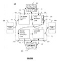
- FIG 3 illustrates the architecture of the asset management device 10 (referred to thereinafter as "order management device"), according to certain embodiments of the invention.
- the order management device 10 is built around a parallel processing device, such as an FPGA, surrounded by external memories, and network interfaces.
- a parallel processing device such as an FPGA
- the order management device 10 generally receives normalized output commands from a data packets decoding device 3. More specifically, the data packet decoding device 3 receives market data streams, and based on the market data streams outputs normalized command 100 for each message that are the same across all the markets, which makes the cores that follow (order management device 10, limits aggregation and book building device 4, etc.) market-independent, and makes it possible to develop these cores only once.
- Each normalized command 100 may comprise an operation code (or "opcode”) that indicates the type of operation to execute, an order ID, and a field for each characteristic of the order (instrument ID, side, price, quantity, etc).
- an extra “valid” signal may be used to flag the command as valid, and a “ready” signal for back pressuring (standard Avalon ST).
- the order management device 10 according to the invention is based on a pipelining approach that allows for the execution of several messages at the same time.
- the pipelined process is divided in smaller processing steps, each part processing one message at a time, so that the whole order management device 10 can process several messages at the same time.
- the order management device 10 according to the invention is in particular provided to address the situations where some of the messages being processed in parallel refer to a same order.
- these messages are treated at the same time, the result is the same as if they had been processed sequentially.
- the order management device 10 By pipelining the order management device 10, more cycles are used for each command because of synchronization and communication issues between the different sub-cores. However, raising the clock frequency is eased because more register stages can be inserted without degrading the performance. Accordingly, the order management device 10 can be used at higher frequencies, matching the frequency of the external memory to use it at its full potential, and canceling the performance degradation caused by the clock cycles used for synchronization and communication. The overall latency of the order management device according to the invention is thus the same as if it were not pipelined, while being able to process commands at a higher throughput.
- the pipelined order management device is in particular arranged to solve the problem of multiple commands with same identifiers.
- the F1 arrows designate the main data path
- the F2 arrows designate the memory reads
- the F3 arrows designate Memory writes.
- figure 3 is only a functional representation of the order management device 10 and that some small support cores (FIFOs between the sub-cores, adapters, memory controllers, etc) are not shown in order to facilitate the comprehension of this figure.
- Each entry in the internal data structures of the order management device 10 is associated with a given order identifier.
- the information related to each order is maintained in a Data Memory 103.
- the information maintained in the data memory 103 may comprise the instrument, the side (bid/sell), the price, and the quantity of the order.
- the order related information is stored in the data memory 103 at an address that is computed from hashes based on the order identifier.
- the Order Identifiers (IDs) in the input messages are used by the order management device as keys to identify the orders.
- the order identifiers are made unique across all the markets processed by the same system by appending a Market identifier to them.
- the order IDs (and thus the keys) may be for example integer number on 64 bits.
- the order management device 10 comprises a Keys Memory 102 for storing information related to the keys associated with the order identifiers.
- the Keys Memory 102 stores words of data, each word of data comprising couples ⁇ key, presence bit ⁇ .
- the key Memory 102 comprises in particular as many couples ⁇ key, presence bit ⁇ as possible to fit in the physical memory. This allows fully using the memory bandwidth when searching for an entry.
- the Keys Memory 102 and the Data Memory 103 may be provided either in internal FPGA memory, or in external memory chips. In a particular embodiment of the invention, both Keys and Data memories 102 and 103 may be provided in the same physical memory. In such embodiment, Keys Memory 102 and Data Memory 103 share the total memory bandwidth, and an arbiter entity may be provided to arbitrate between the concurrent accesses. In particular, the arbiter entity may handle one of the addresses in a way that prevents both memory regions from overlapping.
- the arbiter entity may be further configured to let the commands of one of its inputs through and backpressure the other inputs. It comprises a configurable function for selecting the input which commands are to be let through (configuration may be performed based on a priority or based on round robin). An offset can be added to the address of one of the inputs of the arbiters (addition), at the instantiation of the arbiter, to implement the function for avoiding overlapping between both memory regions.
- the order management device 10 comprises four main components (also referred to thereinafter as "cores") interacting with the key memory 102 and the data memory 103:
- the order management device 10 comprises two parts: the first part, including the first Address Generation Core 101 and the entry allocation core 104, is responsible for keys management, while the second part, including the second address generation core 106 and the execution core 107, is responsible for asset value management.
- the first Address Generation Core 101 comprises hash functions and is configured to generate keys memory read commands (F2) to keys memory 102.
- Each generated command comprises the address of the memory word to read.
- the order ID is hashed by a configurable number of hash functions, generating one or more hashes used as addresses.
- the hash functions represent multiplicative hashes obtained by using an FPGA hardware multiplier
- Hard multipliers are logic circuitry dedicated to multiplications, generally available in FPGAs. Hardware multipliers allow doing multiplications efficiently, using less general-purpose logic. They further allow higher clock speeds to be reached than if the multiplication was done with general-purpose logic. More specifically, the FPGA hardware multiplier is configured to multiply the Order ID by a given coefficient. The higher and lower bits resulting from the multiplication may then be dropped to keep the suitable number of bits to address the whole keys memory. The middle bits are selected because they provide the most variance for any given input bit.
- multiplicative hash is that no additional resource is required (the hardware multipliers are already available) and provides hashes of satisfying quality.
- the invention is not limited to multiplicative hash and that the computation of the hash that can be performed differently, in particular based on logic functions, arithmetical operations, etc.
- Figure 4 is a functional diagram illustrating the generation of hashes 46 from order ID 40, according to certain embodiments of the invention.
- Different hashes 46 may be obtained by varying the coefficient used for the multiplication.
- the core 101 may comprise a list of coefficients 41, chosen randomly (using a multiplexer 42).
- the coefficients 41 may be used sequentially to provide the desired number of hashes 46.
- Pipelining is then achieved by enabling pipelining on the multiplier 45 and latching the order ID during the cycles corresponding to the different hashes computation.
- the latching of the order Identifier may be performed using a latch 44 which may be controlled by a counter or a finite state machine FSM 43.
- the first Address Generation Core 101 generates a different hash for each memory, reducing the effect of hash collisions. Furthermore, better performances may be obtained by providing the keys memory 102 and the data memory 103 on the same physical chips, and by accessing to these chips in parallel.
- the entry allocation core 104 is arranged to perform entry allocation and forwards to the other cores (106, 107) the address and position at which the entry is found or allocated, depending on the type of the input command received by the order management device 10.
- the entry allocation core 104 may allocate a new entry in the keys memory to an order ID in response to an add command.
- the entry allocation core 104 is configured to locate (or find) an entry in the keys memory in response to other types of commands such as a delete or a modify command.
- the entry allocation core 104 receives data words from the keys memory 102, as previously requested by the first Address Generation core 101.
- the entry allocation core 104 may take the first available slot in the received data words returned by the memory 102. More specifically, in response to a command for adding an entry for an order ID, the entry allocation core 104 may look up for an available entry slot in every word of data and if such an empty slot is found, the address of the available entry is sent on the output, along with the position of the slot in the data word and the original input command. If no available entry is found (the memory is full), an error code may be sent.
- the entry allocation core 104 may receive a request from the first Address Generation Core 101. In response to this request, the entry allocation core 104 is configured to look up for an entry that matches the order ID in the input command in every word of data returned by the keys memory 102. If the entry is found, the address of the entry is sent on the output, along with the position of the entry in the data word and the original input command. If the entry associated with the order ID cannot be found (the entry does not exist) an error code may be sent.
- the core 104 does not directly write the allocated entries to the memory so the data read can be out of date.
- the entry allocation core 104 may write the modified entries to memory 102 directly. Yet, even in such embodiments, the data could be outdated. Indeed, the read commands are sent by the keys memory 102 so that a read command could be issued before the entry allocation core 104 has finished processing the previous command. If both commands (current read command and previous read command) concern the same order, or an order stored at the same address because of a collision in the hash function, the data read could be outdated.
- the order management device 10 may further comprise a cache 105 for keeping track of the last processed order identifiers, as well as the addresses and positions at which the corresponding order identifiers have been placed.
- the cache 105 may be comprised in the entry cache and key comparison core 104 and may be seen as a set of registers which are updated at each allocation of an entry in the keys memory (add).
- the second address generation core 106 is provided to generate the read commands to the data memory 103 for storing order information associated with an entry of the keys memory (such as the instrument, the side (bid/sell), the price, and the quantity of the order).
- the data read by the second address generation core 106 are sent by data memory 103 to core 107.
- the order related information is stored in the data memory 103 at an address that is derived from the address and the position in the data word of the key provided by the Entry allocation core 104.
- the order management device 10 may be arranged so as to ensure that, when using the same memory to store the keys and the order data, both memory regions do not overlap (using the arbiter entity).
- the execution core 107 is provided for executing each command.
- the execution core 107 writes the obtained result back to keys memory 102 and data memory 103.
- the execution core 107 receives the data needed to actually process a command. It receives the address of the entry identified in the input command, the input command forwarded from the previous cores on its input interface, and the properties of the considered order (price, quantity, etc) from the data memory 103.
- the execution core 107 is in particular configured to execute the following types of operations:
- the execution core 107 may thus perform two write operations:
- the execution core 107 is the only core that can trigger deletion of orders when the final quantity depends on the quantity in memory, so all the writes operations are done in this core, especially the writes to the keys memory 102.
- the execution core 107 may further comprise a cache as the core 106 generating the read commands (represented by arrows F2) for the data memory 103 is placed before the execution core 107.
- the cache of the execution core 107 comprises the identifier and the properties of the last orders processed.
- the cache information is used to replace the properties read from the data memory 103 when the order ID matches, before actually processing the command.
- the command rate that is accepted does not depend on the number of clock cycle required by the processing. There is accordingly no particular constraint on the number of clock cycles required by the 4 cores 101, 104, 106, and 107. This allows an easy increase on frequency.
- FIG. 5 shows the different steps of the order management method according to the invention.
- step 500 a command related to Order ID is received comprising an order identifier and a set of order information.
- step 501 one or more addresses are computed by hashing Order ID using for example an FPGA multiplier.
- step 502 read commands are emitted at the addresses computed in step 501.
- step 503 data words are read at the requested addresses in the Key Memory 102.
- step 504 the keys in couples ⁇ Key, Presence Bit ⁇ , in the read data, are compared to the Order ID in the input command.
- step 505 If a match has been found with a presence bit equal to 1 (step 505), and if the input command is an ADD command (506), a "memory full" Code is set in step 507. Then, an output command comprising the Input command, and possibly old and updated order Information, and/or an error code is sent at step 508.
- step 510 the address of the data portion of the order is computed using the address and position information transmitted in step 509. Then, in step 511, data words are read from Data memory 103, at the requested address. Order Data may be then created or updated using input command in step 512, and the updated Order Data may be written back to data memory 103.
- step 516 it is determined if the Updated Quantity is null and if so, in step 517, the presence bit is set to zero in keys memory 102. In both cases, the output command comprising the Input command, with possibly the old and updated order information, and/or an error code are sent in step 508.
- step 505 if no match has been found (or if a match has been found but with a presence bit different from 1), and if the input command is an ADD command (518), an entry corresponding to Order ID is allocated in step 519 (by updating local cache of Core 104) and in step 509 the Address and position at which the key has been allocated are transmitted to the Data Address generation Core 106. Execution Steps 510, 511, 512, 513, 514, 515, 508, 516, and 517 may be then performed.
- step 518 If it is determined that the input command is not an ADD command, in step 518, an "Order Not Found” Code is set (520) and then step 508 is performed to send an output command comprising the Input command, with the old and updated order information and/or an error code if any.
- Figure 6 represents an exemplary Asset Management device according to certain embodiments of the invention. More particularly, it represents partial views of the Key memory 102 and the Data memory 103. Each line in the memory 102 or 103 represents a word of data. Keys memory 102 comprises 2 couples ⁇ presence bit, key ⁇ per word. Data memory 103 comprises one value per word. The presence bits in keys memory 102 are not represented.
- the asset management device 10 can process more messages per unit of time than conventional asset management devices.
- the four-fold structure of the asset management device 10 (cores 101, 104, 106 and 107) and the interactions between the cores also contribute to the obtained performances.
- pipelined design of the asset management device allows for an easier increase in frequency, and thus for satisfying performances.
- Another advantage of the invention is related to the fact that the entry allocation core 104 can read a maximum number of keys per clock cycles, thereby fully using the memory bandwidth.
- caches in the entry allocation core 104 and the execution core 107 make it possible to achieve an efficient pipelined design.
- the asset management device 10 is adapted to directly integrate the business logic. This avoids round trips between a standard hash table and a business core which would instantiate the hash table. For example, for modifications that would involve a null quantity, incorporating the business logic in the core obviates the needs for the following steps:
- the business logic can be integrated to only a part of the asset management device 10: in the example of a market data processing application, it may be integrated to only a part of the core 107 related to the financial application. Specificities can then be contained and easily maintained or modified.
Landscapes
- Engineering & Computer Science (AREA)
- Theoretical Computer Science (AREA)
- Physics & Mathematics (AREA)
- Computer Security & Cryptography (AREA)
- Computer Hardware Design (AREA)
- General Physics & Mathematics (AREA)
- Software Systems (AREA)
- Business, Economics & Management (AREA)
- General Engineering & Computer Science (AREA)
- Finance (AREA)
- Accounting & Taxation (AREA)
- Mathematical Physics (AREA)
- Signal Processing (AREA)
- Computer Networks & Wireless Communication (AREA)
- Development Economics (AREA)
- Economics (AREA)
- Marketing (AREA)
- Strategic Management (AREA)
- Technology Law (AREA)
- General Business, Economics & Management (AREA)
- Information Retrieval, Db Structures And Fs Structures Therefor (AREA)
- Retry When Errors Occur (AREA)
Priority Applications (8)
| Application Number | Priority Date | Filing Date | Title |
|---|---|---|---|
| EP13306356.0A EP2858024A1 (de) | 2013-10-01 | 2013-10-01 | Bestandsverwaltungsvorrichtung und -verfahren in einer Hardware-Plattform |
| US14/502,963 US9535702B2 (en) | 2013-10-01 | 2014-09-30 | Asset management device and method in a hardware platform |
| SG11201602342PA SG11201602342PA (en) | 2013-10-01 | 2014-10-01 | An asset management device and method in a hardware platform |
| CA2925805A CA2925805A1 (en) | 2013-10-01 | 2014-10-01 | An asset management device and method in a hardware platform |
| HK16113657.9A HK1225462B (zh) | 2013-10-01 | 2014-10-01 | 硬件平台中的资产管理设备和方法 |
| CN201480054765.1A CN105637524B (zh) | 2013-10-01 | 2014-10-01 | 硬件平台中的资产管理设备和方法 |
| AU2014331142A AU2014331142B2 (en) | 2013-10-01 | 2014-10-01 | An asset management device and method in a hardware platform |
| PCT/EP2014/071071 WO2015049304A1 (en) | 2013-10-01 | 2014-10-01 | An asset management device and method in a hardware platform |
Applications Claiming Priority (1)
| Application Number | Priority Date | Filing Date | Title |
|---|---|---|---|
| EP13306356.0A EP2858024A1 (de) | 2013-10-01 | 2013-10-01 | Bestandsverwaltungsvorrichtung und -verfahren in einer Hardware-Plattform |
Publications (1)
| Publication Number | Publication Date |
|---|---|
| EP2858024A1 true EP2858024A1 (de) | 2015-04-08 |
Family
ID=49328475
Family Applications (1)
| Application Number | Title | Priority Date | Filing Date |
|---|---|---|---|
| EP13306356.0A Pending EP2858024A1 (de) | 2013-10-01 | 2013-10-01 | Bestandsverwaltungsvorrichtung und -verfahren in einer Hardware-Plattform |
Country Status (7)
| Country | Link |
|---|---|
| US (1) | US9535702B2 (de) |
| EP (1) | EP2858024A1 (de) |
| CN (1) | CN105637524B (de) |
| AU (1) | AU2014331142B2 (de) |
| CA (1) | CA2925805A1 (de) |
| SG (1) | SG11201602342PA (de) |
| WO (1) | WO2015049304A1 (de) |
Families Citing this family (10)
| Publication number | Priority date | Publication date | Assignee | Title |
|---|---|---|---|---|
| US10452971B2 (en) * | 2015-06-29 | 2019-10-22 | Microsoft Technology Licensing, Llc | Deep neural network partitioning on servers |
| CN106130752B (zh) * | 2016-06-10 | 2023-04-07 | 北京数盾信息科技有限公司 | 一种基于gdoi协议下大规模网络管理系统 |
| CN109284822B (zh) * | 2017-07-20 | 2021-09-21 | 上海寒武纪信息科技有限公司 | 一种神经网络运算装置及方法 |
| US10880211B2 (en) | 2019-05-06 | 2020-12-29 | Seth Gregory Friedman | Transaction encoding and verification by way of data-link layer fields |
| US10868707B1 (en) | 2019-09-16 | 2020-12-15 | Liquid-Markets-Holdings, Incorporated | Zero-latency message processing with validity checks |
| CN111177476B (zh) * | 2019-12-05 | 2023-08-18 | 北京百度网讯科技有限公司 | 数据查询方法、装置、电子设备及可读存储介质 |
| EP4144048A4 (de) | 2020-06-08 | 2024-06-26 | Liquid-Markets GmbH | Hardwarebasierter transaktionsaustausch |
| CN113609136B (zh) * | 2021-08-26 | 2022-04-26 | 深圳市链融科技股份有限公司 | 业务编号稳定保持方法、装置、计算机设备及存储介质 |
| US11915065B2 (en) * | 2022-01-20 | 2024-02-27 | Vmware, Inc. | Brokerless reliable totally ordered many-to-many interprocess communication on a single node that uses shared memory and multicast |
| US20240193090A1 (en) * | 2022-12-07 | 2024-06-13 | Hyannis Port Research, Inc. | Cache structure for high performance hardware based processor |
Citations (4)
| Publication number | Priority date | Publication date | Assignee | Title |
|---|---|---|---|---|
| EP0411691A2 (de) * | 1989-07-31 | 1991-02-06 | Koninklijke Philips Electronics N.V. | Speicherarchitektur und Schaltung zum Hashcodieren |
| US5032987A (en) * | 1988-08-04 | 1991-07-16 | Digital Equipment Corporation | System with a plurality of hash tables each using different adaptive hashing functions |
| US20030182291A1 (en) * | 2002-03-20 | 2003-09-25 | Sreenath Kurupati | Method and data structure for a low memory overhead database |
| US20080243675A1 (en) * | 2006-06-19 | 2008-10-02 | Exegy Incorporated | High Speed Processing of Financial Information Using FPGA Devices |
-
2013
- 2013-10-01 EP EP13306356.0A patent/EP2858024A1/de active Pending
-
2014
- 2014-09-30 US US14/502,963 patent/US9535702B2/en active Active
- 2014-10-01 WO PCT/EP2014/071071 patent/WO2015049304A1/en not_active Ceased
- 2014-10-01 AU AU2014331142A patent/AU2014331142B2/en not_active Ceased
- 2014-10-01 CA CA2925805A patent/CA2925805A1/en active Pending
- 2014-10-01 CN CN201480054765.1A patent/CN105637524B/zh not_active Expired - Fee Related
- 2014-10-01 SG SG11201602342PA patent/SG11201602342PA/en unknown
Patent Citations (5)
| Publication number | Priority date | Publication date | Assignee | Title |
|---|---|---|---|---|
| US5032987A (en) * | 1988-08-04 | 1991-07-16 | Digital Equipment Corporation | System with a plurality of hash tables each using different adaptive hashing functions |
| EP0411691A2 (de) * | 1989-07-31 | 1991-02-06 | Koninklijke Philips Electronics N.V. | Speicherarchitektur und Schaltung zum Hashcodieren |
| US20030182291A1 (en) * | 2002-03-20 | 2003-09-25 | Sreenath Kurupati | Method and data structure for a low memory overhead database |
| US20080243675A1 (en) * | 2006-06-19 | 2008-10-02 | Exegy Incorporated | High Speed Processing of Financial Information Using FPGA Devices |
| US7921046B2 (en) | 2006-06-19 | 2011-04-05 | Exegy Incorporated | High speed processing of financial information using FPGA devices |
Non-Patent Citations (3)
| Title |
|---|
| CHALAMALASETTI SAI RAHUL ET AL: "An FPGA memcached appliance", FPGA '13: PROCEEDINGS OF THE ACM/SIGDA INTERNATIONAL SYMPOSIUM ON FIELD PROGRAMMABLE GATE ARRAYS, 11 February 2013 (2013-02-11), New York, NY, USA, pages 245 - 254, XP093134437, ISBN: 978-1-4503-1887-7, Retrieved from the Internet <URL:https://dl.acm.org/doi/pdf/10.1145/2435264.2435306> * |
| ISTVAN ZSOLT ET AL: "A flexible hash table design for 10GBPS key-value stores on FPGAS", 2013 23RD INTERNATIONAL CONFERENCE ON FIELD PROGRAMMABLE LOGIC AND APPLICATIONS, IEEE, 2 September 2013 (2013-09-02), pages 1 - 8, XP032514417, DOI: 10.1109/FPL.2013.6645520 * |
| JOHN CIESLEWICZ ET AL: "Adaptive Aggregation on Chip Multiprocessors", 25 September 2007 (2007-09-25), XP055104309, Retrieved from the Internet <URL:http://www.vldb.org/conf/2007/papers/research/p339-cieslewicz.pdf> [retrieved on 20140225] * |
Also Published As
| Publication number | Publication date |
|---|---|
| HK1225462A1 (zh) | 2017-09-08 |
| CN105637524A (zh) | 2016-06-01 |
| AU2014331142B2 (en) | 2020-05-21 |
| CN105637524B (zh) | 2019-06-07 |
| WO2015049304A1 (en) | 2015-04-09 |
| AU2014331142A1 (en) | 2016-04-21 |
| US20150095613A1 (en) | 2015-04-02 |
| SG11201602342PA (en) | 2016-04-28 |
| US9535702B2 (en) | 2017-01-03 |
| CA2925805A1 (en) | 2015-04-09 |
Similar Documents
| Publication | Publication Date | Title |
|---|---|---|
| EP2858024A1 (de) | Bestandsverwaltungsvorrichtung und -verfahren in einer Hardware-Plattform | |
| EP2858025B1 (de) | Auftragsbuchsverwaltungsvorrichtung in einer hardware-plattform | |
| JP5871619B2 (ja) | 金融市場深度データの高速処理のための方法および装置 | |
| US11256431B1 (en) | Storage system having a field programmable gate array | |
| CN101053234B (zh) | 用于越过具有进入的分组数据的dfa图像的方法和装置 | |
| US8301788B2 (en) | Deterministic finite automata (DFA) instruction | |
| US10127275B2 (en) | Mapping query operations in database systems to hardware based query accelerators | |
| US20130103654A1 (en) | Global dictionaries using universal primitives | |
| CN110119304B (zh) | 一种中断处理方法、装置及服务器 | |
| US20230289343A1 (en) | Allocating partitions for executing operations of a query | |
| US10244017B2 (en) | Processing of streaming data with a keyed join | |
| WO2018205689A1 (zh) | 合并文件的方法、存储装置、存储设备和存储介质 | |
| CN113194127B (zh) | 一种数据存储方法、数据传输方法及计算设备 | |
| US11249916B2 (en) | Single producer single consumer buffering in database systems | |
| Preußer et al. | Using dsp slices as content-addressable update queues | |
| US8122221B2 (en) | Method and apparatus to combine scattered buffer addresses into a contiguous virtual address space | |
| HK1225462B (zh) | 硬件平台中的资产管理设备和方法 | |
| US20240193090A1 (en) | Cache structure for high performance hardware based processor | |
| US20170026302A1 (en) | Systems and methods for reorganization of messages in queuing systems | |
| CN121235135A (zh) | 量子计算任务的执行方法、量子计算机及可读存储介质 | |
| CN119536916A (zh) | 接口配置管理方法、装置、计算机设备、可读存储介质和程序产品 | |
| CN120658369A (zh) | 一种高效的基于全同态加密的隐私求交方法及装置 | |
| HK1225841B (zh) | 硬件平台中的订单账簿管理设备 |
Legal Events
| Date | Code | Title | Description |
|---|---|---|---|
| PUAI | Public reference made under article 153(3) epc to a published international application that has entered the european phase |
Free format text: ORIGINAL CODE: 0009012 |
|
| 17P | Request for examination filed |
Effective date: 20131001 |
|
| AK | Designated contracting states |
Kind code of ref document: A1 Designated state(s): AL AT BE BG CH CY CZ DE DK EE ES FI FR GB GR HR HU IE IS IT LI LT LU LV MC MK MT NL NO PL PT RO RS SE SI SK SM TR |
|
| AX | Request for extension of the european patent |
Extension state: BA ME |
|
| R17P | Request for examination filed (corrected) |
Effective date: 20151008 |
|
| RBV | Designated contracting states (corrected) |
Designated state(s): AL AT BE BG CH CY CZ DE DK EE ES FI FR GB GR HR HU IE IS IT LI LT LU LV MC MK MT NL NO PL PT RO RS SE SI SK SM TR |
|
| STAA | Information on the status of an ep patent application or granted ep patent |
Free format text: STATUS: EXAMINATION IS IN PROGRESS |
|
| 17Q | First examination report despatched |
Effective date: 20170116 |
|
| 19A | Proceedings stayed before grant |
Effective date: 20171006 |
|
| 19F | Resumption of proceedings before grant (after stay of proceedings) |
Effective date: 20230201 |
|
| RAP3 | Party data changed (applicant data changed or rights of an application transferred) |
Owner name: EXEGY |