EP2855729B1 - Verfahren zur beschichtung eines substrats und beschichter - Google Patents
Verfahren zur beschichtung eines substrats und beschichter Download PDFInfo
- Publication number
- EP2855729B1 EP2855729B1 EP12724615.5A EP12724615A EP2855729B1 EP 2855729 B1 EP2855729 B1 EP 2855729B1 EP 12724615 A EP12724615 A EP 12724615A EP 2855729 B1 EP2855729 B1 EP 2855729B1
- Authority
- EP
- European Patent Office
- Prior art keywords
- rotatable
- cathodes
- rotatable cathodes
- substrate
- pair
- Prior art date
- Legal status (The legal status is an assumption and is not a legal conclusion. Google has not performed a legal analysis and makes no representation as to the accuracy of the status listed.)
- Active
Links
Images


Classifications
-
- C—CHEMISTRY; METALLURGY
- C23—COATING METALLIC MATERIAL; COATING MATERIAL WITH METALLIC MATERIAL; CHEMICAL SURFACE TREATMENT; DIFFUSION TREATMENT OF METALLIC MATERIAL; COATING BY VACUUM EVAPORATION, BY SPUTTERING, BY ION IMPLANTATION OR BY CHEMICAL VAPOUR DEPOSITION, IN GENERAL; INHIBITING CORROSION OF METALLIC MATERIAL OR INCRUSTATION IN GENERAL
- C23C—COATING METALLIC MATERIAL; COATING MATERIAL WITH METALLIC MATERIAL; SURFACE TREATMENT OF METALLIC MATERIAL BY DIFFUSION INTO THE SURFACE, BY CHEMICAL CONVERSION OR SUBSTITUTION; COATING BY VACUUM EVAPORATION, BY SPUTTERING, BY ION IMPLANTATION OR BY CHEMICAL VAPOUR DEPOSITION, IN GENERAL
- C23C14/00—Coating by vacuum evaporation, by sputtering or by ion implantation of the coating forming material
- C23C14/22—Coating by vacuum evaporation, by sputtering or by ion implantation of the coating forming material characterised by the process of coating
- C23C14/34—Sputtering
- C23C14/35—Sputtering by application of a magnetic field, e.g. magnetron sputtering
- C23C14/352—Sputtering by application of a magnetic field, e.g. magnetron sputtering using more than one target
-
- H—ELECTRICITY
- H01—ELECTRIC ELEMENTS
- H01J—ELECTRIC DISCHARGE TUBES OR DISCHARGE LAMPS
- H01J37/00—Discharge tubes with provision for introducing objects or material to be exposed to the discharge, e.g. for the purpose of examination or processing thereof
- H01J37/32—Gas-filled discharge tubes
- H01J37/34—Gas-filled discharge tubes operating with cathodic sputtering
- H01J37/3464—Operating strategies
- H01J37/3473—Composition uniformity or desired gradient
-
- C—CHEMISTRY; METALLURGY
- C23—COATING METALLIC MATERIAL; COATING MATERIAL WITH METALLIC MATERIAL; CHEMICAL SURFACE TREATMENT; DIFFUSION TREATMENT OF METALLIC MATERIAL; COATING BY VACUUM EVAPORATION, BY SPUTTERING, BY ION IMPLANTATION OR BY CHEMICAL VAPOUR DEPOSITION, IN GENERAL; INHIBITING CORROSION OF METALLIC MATERIAL OR INCRUSTATION IN GENERAL
- C23C—COATING METALLIC MATERIAL; COATING MATERIAL WITH METALLIC MATERIAL; SURFACE TREATMENT OF METALLIC MATERIAL BY DIFFUSION INTO THE SURFACE, BY CHEMICAL CONVERSION OR SUBSTITUTION; COATING BY VACUUM EVAPORATION, BY SPUTTERING, BY ION IMPLANTATION OR BY CHEMICAL VAPOUR DEPOSITION, IN GENERAL
- C23C14/00—Coating by vacuum evaporation, by sputtering or by ion implantation of the coating forming material
- C23C14/22—Coating by vacuum evaporation, by sputtering or by ion implantation of the coating forming material characterised by the process of coating
- C23C14/34—Sputtering
- C23C14/35—Sputtering by application of a magnetic field, e.g. magnetron sputtering
-
- H—ELECTRICITY
- H01—ELECTRIC ELEMENTS
- H01J—ELECTRIC DISCHARGE TUBES OR DISCHARGE LAMPS
- H01J37/00—Discharge tubes with provision for introducing objects or material to be exposed to the discharge, e.g. for the purpose of examination or processing thereof
- H01J37/32—Gas-filled discharge tubes
- H01J37/32431—Constructional details of the reactor
- H01J37/32532—Electrodes
- H01J37/32568—Relative arrangement or disposition of electrodes; moving means
-
- H—ELECTRICITY
- H01—ELECTRIC ELEMENTS
- H01J—ELECTRIC DISCHARGE TUBES OR DISCHARGE LAMPS
- H01J37/00—Discharge tubes with provision for introducing objects or material to be exposed to the discharge, e.g. for the purpose of examination or processing thereof
- H01J37/32—Gas-filled discharge tubes
- H01J37/34—Gas-filled discharge tubes operating with cathodic sputtering
- H01J37/3402—Gas-filled discharge tubes operating with cathodic sputtering using supplementary magnetic fields
- H01J37/3405—Magnetron sputtering
-
- H—ELECTRICITY
- H01—ELECTRIC ELEMENTS
- H01J—ELECTRIC DISCHARGE TUBES OR DISCHARGE LAMPS
- H01J37/00—Discharge tubes with provision for introducing objects or material to be exposed to the discharge, e.g. for the purpose of examination or processing thereof
- H01J37/32—Gas-filled discharge tubes
- H01J37/34—Gas-filled discharge tubes operating with cathodic sputtering
- H01J37/3411—Constructional aspects of the reactor
- H01J37/3414—Targets
- H01J37/3417—Arrangements
-
- H—ELECTRICITY
- H01—ELECTRIC ELEMENTS
- H01J—ELECTRIC DISCHARGE TUBES OR DISCHARGE LAMPS
- H01J2237/00—Discharge tubes exposing object to beam, e.g. for analysis treatment, etching, imaging
- H01J2237/32—Processing objects by plasma generation
- H01J2237/33—Processing objects by plasma generation characterised by the type of processing
- H01J2237/332—Coating
- H01J2237/3322—Problems associated with coating
- H01J2237/3323—Problems associated with coating uniformity
Definitions
- the present disclosure relates to a method for coating a substrate, a coater for coating a substrate, and a controller for controlling a coating process. More specifically, it relates to a method for coating a substrate and a coater for coating substrates, in particular by sputtering. More specifically, the present disclosure is directed at magnetron sputtering wherein the cathode is typically a rotatable cathode including a rotatable target. Even more specifically, the method and the coater are directed at static sputtering deposition.
- the present disclosure particularly relates to substrate coating technology solutions involving equipment, processes and materials used in the deposition, patterning, and treatment of substrates and coatings, with representative examples including (but not limited to) applications involving: semiconductor and dielectric materials and devices, silicon-based wafers, flat panel displays (such as TFTs), masks and filters, energy conversion and storage (such as photovoltaic cells, fuel cells, and batteries), solid-state lighting (such as LEDs and OLEDs), magnetic and optical storage, micro-electro-mechanical systems (MEMS) and nano-electro-mechanical systems (NEMS), micro-optic and opto-elecro-mechanical systems (NEMS), micro-optic and optoelectronic devices, transparent substrates, architectural and automotive glasses, metallization systems for metal and polymer foils and packaging, and micro- and nano-molding.
- MEMS micro-electro-mechanical systems
- NEMS nano-electro-mechanical systems
- NEMS micro-optic and opto-elecro-mechanical systems
- a thin layer of a coating material In many applications, it is desired to deposit a thin layer of a coating material on a substrate.
- Known techniques for depositing layers are, in particular, evaporating and sputtering.
- Sputtering is a vacuum coating process used to deposit thin films of various materials onto the surface of a substrate.
- sputtering can be used to deposit a metal layer such as a thin layer of aluminium or ceramics or an oxide layer.
- the coating material is transported, from a target consisting of that material, to the substrate to be coated by bombarding the surface of the target with ions of an inert gas or reactive gas that are accelerated by a high voltage.
- the gas ions hit the outer surface of the target their momentum is transferred to the atoms of the material so that some of them can gain sufficient energy to overcome their bonding energy in order to escape from the target surface and to deposit on the substrate. Thereon, they form a film of the desired material.
- the thickness of the deposited film is, inter alia, dependent on the duration of exposing the substrate to the sputtering process.
- the thickness of the deposited layer on the substrate is as uniform as possible throughout the whole substrate. It is further desired to have a high degree of homogeneity in terms of characteristics such as the grown crystal structure, the specific resistance, the stress of the layer, and optical characteristics. For instance, in the production of metalized layers the signal delay is dependent on the thickness of the layer so that, e.g., in the production of displays a varying thickness might result in pixels that are energized at slightly different times. It is further important to rely on a uniform layer thickness when etching a layer in order to achieve the same results at different positions. Furthermore, the costs of the deposition process shall be as low as possible.
- a method for coating a substrate and a coater for coating a substrate is provided.
- a method for coating a substrate by means of a cathode arrangement including at least two rotatable cathodes includes rotating at least one of the at least two rotatable cathodes in a first direction, and, at the same time, rotating at least one of the at least two rotatable cathodes in a second direction.
- the first direction is opposite to the second direction.
- a controller for controlling a coating process is disclosed.
- the controller is adapted for performing the method for coating a substrate by means of a cathode arrangement as disclosed herein.
- a coater for coating a substrate includes a cathode arrangement with at least two rotatable cathodes and a controller as disclosed herein.
- Embodiments are also directed to apparatuses for carrying out each of the disclosed methods and including apparatus parts for performing each described method step. These method steps may be performed by way of hardware components, a computer program by appropriate software, by any combination of the two or in any other manner. Furthermore, embodiments are also directed to methods by which the described apparatus operates or by which the described apparatus is manufactured. It includes method steps for carrying out functions of this apparatus or manufacturing parts of the apparatus.
- the process of coating a substrate with a material as described herein refers typically to thin-film applications.
- coating and the term “depositing” are used synonymously herein.
- substrate as used herein shall include both inflexible substrates, e.g., a wafer or a glass plate, and flexible substrates, such as, webs and foils. In most cases, the substrate is an inflexible substrate, such as, a glass plate, e.g., used in the production of a display.
- the typical coating process used in embodiments described herein is sputtering.
- sputtering can be undertaken as diode sputtering or magnetron sputtering.
- the magnetron sputtering is particularly advantageous in that its deposition rates are rather high.
- at least one magnet is positioned within the rotatable cathode, for instance, one magnet or two magnets.
- the magnet is movably arranged within the rotatable cathode.
- the rotatable cathode as used herein is typically a rotatable curved cathode including a rotatable curved target.
- the substrate may be continuously moved during coating (“dynamic coating”) or the substrate to be coated rests during coating (“static coating”).
- Static coating is advantageous in that the amount of target material used up for the coating is smaller in comparison to dynamic coating since in the latter case the substrate holders are often coated as well.
- Static coating particularly allows the coating of large-area substrates. The substrates are entered into a coating area, the coating is performed, and the substrates are taken out of the coating area again.
- the present disclosure specifically relates to static coating.
- Sputtering can be used in the production of displays.
- sputtering may be used for the metallization such as the generation of electrodes or buses. It is also used for the generation of thin film transistors (TFTs), such as in LCD applications. It may also be used for the generation of transparent conductive layers, such as an ITO (indium tin oxide) layer, in particular for colour filter applications and/or pixel ITO applications.
- TFTs thin film transistors
- transparent conductive layers such as an ITO (indium tin oxide) layer, in particular for colour filter applications and/or pixel ITO applications.
- the deposited layer may be configured to form the lower electrode of a TFT stack.
- a thin-film solar cell comprises a back contact, an absorbing layer, and a transparent and conductive oxide layer (TCO).
- TCO transparent and conductive oxide layer
- the back contact and the TCO layer is produced by sputtering whereas the absorbing layer is typically made in a chemical vapour deposition process.
- sputtering is advantageous in that there are materials which can be sputtered but cannot be evaporated. Further, the adhesion of the produced layers to the substrate is typically stronger in sputtering processes than in evaporation processes. Further, sputtering is a directional process so that the major part of the material is transferred to the substrate and does not coat the interior of the deposition apparatus (as in evaporation applications). The present disclosure specifically relates to sputtering.
- the coater as described herein is typically a sputter apparatus and the rotatable cathodes are rotatable sputter cathodes.
- the plurality of rotatable cathodes provided according to aspects of the present disclosure shall be called “cathode arrangement” herein.
- the term “cathode” and “cathode assembly” shall be used synonymously herein.
- magnet assembly or "magnet” as used herein is a unit capable of generating a magnetic field.
- the magnet assembly consists of a permanent magnet.
- This permanent magnet is typically arranged within the rotatable cathode.
- the magnet assembly comprises a magnet yoke.
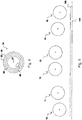
- Fig. 1 schematically illustrates a substrate 100 being positioned on a substrate holder 110.
- the cathode arrangement 1 is illustrated as including an array of rotatable cathodes, namely, six rotatable cathodes 10, 11, 12, 13, 14, and 15 positioned adjacent to the substrate 100 in a sequence.
- a negative potential as compared to the potential at the substrate may be applied to the rotatable cathodes.
- the housing serves as the anode.
- the figures illustrate cross sectional schematic views of coaters along with exemplarily shown substrates.
- the rotatable cathodes have the shape of a cylinder.
- the cathode extends into the paper and out of the paper when looking at the drawings.
- the same is true with respect to the magnet assemblies discussed later on that are also only schematically shown as cross sectional elements.
- the magnet assemblies may extend along the complete length of the cylinder. For technical reasons, it is typical that they extend along at least 80 % of the cylinder length, more typically along at least 90 % of the rotatable cathodes' length.
- the number of rotatable cathodes in an array of rotatable cathodes is an even number, for instance, two, four, six, eight, ten, twelve, fourteen etc.
- every two of the adjacent rotatable cathodes can be linguistically combined and called "a pair of rotatable cathodes".
- a pair of rotatable cathodes as used herein it is understood that the two rotatable cathodes of the pair of rotatable cathodes are positioned adjacent to each other. Hence, sometimes they may also be referred to as "a pair of adjacent rotatable cathodes".
- the outer part of the rotatable cathode that is, the target
- some parts of the rotatable cathode are typically not adapted to be rotated. These parts shall be referred to as the "inner part" of the rotatable target.
- the rotatable cathodes are rotatable along their longitudinal axes. According to the presently described embodiments, each of the rotatable cathodes can be rotated in a first direction (such as the clockwise direction) or the second direction (such as the counter-clockwise direction). The first direction is the rotation direction opposite to the second direction. According to aspects described herein, at least one rotatable cathode rotates in the first direction meanwhile at least one rotatable cathode rotates in the second direction. Typically, if an even number of rotatable cathodes is provided, the number of rotatable cathodes rotating in the first direction equals the number of rotatable cathodes rotating in the second direction.
- the number of rotatable cathodes in an array may also be an uneven number, such as nine, eleven, thirteen or fifteen. If an uneven number of rotatable cathodes are provided, such as 2n + 1 rotatable cathodes, it is typical that n rotatable cathodes rotate in the first direction whereas n + 1 rotatable cathodes rotate in the second direction.
- the influence of the outermost rotatable cathode (which is typically the 2n + 1- th rotatable cathode) on the substrate homogeneity and uniformity is smaller as compared to rotatable cathodes positioned closer to the substrate's center because, according to embodiments, the one or two outermost rotatable cathodes might be positioned in a protruding manner adjacent to the substrate in order to reduce edge effects during sputtering.
- the coater as illustrated in Fig. 1 includes six rotatable cathodes 10-15. It shall be understood that this is for exemplary purposes, and the coater might also include more or less than six rotatable cathodes, such as ten.
- each of the rotatable cathodes has one neighbouring rotatable cathode (such as the rotatable cathodes 10 and 15 in Fig. 1 ) or two neighbouring rotatable cathodes (such as the rotatable cathodes 11, 12, 13, and 14 in Fig. 1 ).
- the term "neighbouring” shall be used to mean “adjacent" herein. It shall refer to the rotatable cathode(s) next to the rotatable cathode under consideration. For instance, the neighbouring cathodes of rotatable cathode 12 are rotatable cathodes 11 and 13.
- each rotatable cathode rotates in a direction that is opposite to the rotational direction of its one or two neighbours.
- the rotatable cathodes may rotate in an alternating manner, that is, the rotatable cathodes 10, 12, and 14 could rotate in the first direction, whereas, at the same time, the rotatable cathodes 11, 13, and 15 may rotate in the second direction, i.e., in an opposite direction to the first direction.
- a number of neighbouring rotatable cathodes rotate in the first direction, and the rest of the cathode arrangement rotates, at the same time, in the opposite direction, for instance, the rotatable cathodes 10, 11, and 12 may rotate in the first direction, whereas at the same time the rotatable cathodes 13, 14, and 15 rotate in the second direction.
- the rotatable cathodes 10, 11, and 14 rotate in the first direction, whereas at the same time the rotatable cathodes 12, 13, and 15 rotate in the second direction.
- the rotation direction of the at least one rotatable cathode is not altered during the coating process.
- the rotational direction of all rotatable cathodes is not altered during the coating process.
- the coating process as understood herein may include or consist of the coating of one substrate.
- the rotation speed of the rotatable cathodes may be constant, such as for the complete sputtering process.
- the rotation speed of one or more of the rotatable cathodes may be non-constant. Either way, it is typical that the rotation speed of all rotatable cathodes of the cathode arrangement is identical, notwithstanding the rotation direction.
- the distance of the rotatable cathodes to the substrate may be different.
- the term "distance" between cathodes as understood herein refers to the distance between center axis and center axis of the cathodes.
- the distance of the rotatable cathodes, that are positioned closer to the substrate's edges, to the substrate may be smaller than the distance of the rotatable cathodes positioned further away from the substrate's edges (i.e., towards or in the center of the substrate).
- the distance as understood in this context is the length of a virtual line leading from the axis of the rotatable cathode to the substrate whereas the virtual line hits the substrate's surface in a perpendicular manner.
- FIG. 1 Such an arrangement with different distances between substrate 110 and the cathodes is illustrated in Figs. 1-5 and Fig. 7 .
- the center axis of the rotatable axis is denoted with reference number 21.
- the outermost rotatable cathode 10 is positioned closest to the substrate, namely, at a distance that is illustrated by the dotted line 22.
- the rotatable cathode 11 is positioned further away from the substrate, and the rotatable cathode 12 is positioned furthest away from the substrate, namely, at a distance illustrated by the dotted line 23.
- the ratio of the distance of the one or more targets positioned closest to the substrate (e.g., targets 10 and 15 in Fig. 1 ) to the distance of the one or more targets positioned furthest away from the substrate (e.g., targets 12 and 13 in Fig. 1 ) may be in the range of 0.6 to 0.8.
- the cathodes furthest away from the substrate may be arranged at a distance of between 170 mm and 250 mm.
- the cathodes closest to the substrate may be arranged at a distance of between 110 mm and 200 mm.
- the coating process is not interrupted. Instead, throughout the deposition, a selectable number of rotatable cathodes rotate in one direction whereas a selectable number of rotatable cathodes rotate in the opposite direction.
- the rotatable cathodes rotate in an opposite direction in an alternating manner, for instance, every second rotatable cathode rotates in the first direction, and the rotatable cathodes between every second rotatable cathode rotate in the second direction.
- the rotatable cathodes are typically arranged in an array in a manner so as to face a substrate, as illustrated in all the figures. However, as discussed already, the distance between each rotatable cathode and the substrate might differ.
- the inventors of the present application found out that the proposed method of coating leads to an improved homogeneity and thus to an improved resistance distribution over the substrate.
- the typical sputter materials are IO (Indium-Oxide), ITO (Indium-Tin-Oxide), IZO (Indium-Zinc-Oxide), IGZO (Indium-Gallium-Zinc-Oxide). Those materials may be sputtered in a partly reactive manner.
- the target may be comprised of metals such as Cu (copper), Molybdenum (Mo) and Titanium (Ti). Those materials may be sputtered in a nonreactive manner.
- the reactive sputter processes may provide deposited oxides of the target materials, such as, of the target materials listed. However, nitrides or oxi-nitrides might be deposited as well. According to yet further embodiments, the target material can also be selected from the group consisting of aluminium (for instance, thereby generating A1 2 0 3 ), silicon, tantalum and niobium.
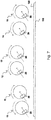
- Fig. 2 illustrates an embodiment including anodes 35.
- a positive potential is applied to the anodes, and they are positioned between the rotatable cathodes.
- the anodes may be provided between each of the neighbouring rotatable cathodes.
- Such an anode may generally have the shape of a bar, with the bar's axis being typically arranged in parallel to the axis of the angular tube.
- a separate bias voltage may be applied to the substrate.
- the provision and use of the anodes is possible with all embodiments described herein, however, for reasons of clarity, the anodes are explicitly depicted only with respect to Figs. 2 and 3 .
- the anodes may be provided in between pairs of cathodes that will be discussed later on in more detail.
- Fig. 3 illustrates an embodiment wherein the magnet assemblies 25 are schematically shown located within the rotatable cathodes 10-15.
- a typical permanent magnet as used in embodiments described herein has two north magnetic poles and a south magnet pole. These poles refer each to a surface of the magnet assembly. The surfaces typically face the rotatable cathode from its inside.
- the cathodes are arranged at the same distance with respect to the substrate surface.
- the cathodes are exemplarily illustrated as having the identical distance to each other. Any combination of these features is possible according to embodiments described herein.
- the cathodes of the embodiment of Fig. 3 could also be arranged on an arc, as exemplarily described with respect to Figs. 1 , 2 , 6 , 7 , and 9 .
- the number of cathodes may be any other number than six, for instance, ten.
- the description of the magnets as illustrated in Fig. 3 is also applicable to all other embodiments described herein, in particular with respect to the embodiments having pairs of cathodes.
- the anodes 35 shown in Fig. 3 are not mandatory but other types of anodes can generally be employed.
- one pole is positioned in the middle whereas two opposite poles are arranged adjacent to it.
- Fig. 3 an enlargement of the magnet assembly 25 is shown for illustrating such a situation.
- the south pole is positioned in the middle, whereas the north poles enframe the south poles.
- the pole surfaces' shape may be adapted to the curvature of the rotatable curved target they are positioned in.
- the substrate's surface defines a plane; the cross-section of which is shown in the figures.
- the orientation of the substrate spatially can be horizontal or vertical.
- the term "vertical" refers to the plane of the substrate. In other embodiments, it is even possible to arrange the substrate somewhere between a horizontal and a vertical orientation.
- large area substrates or respective carriers wherein the carriers have a plurality of substrates, may have a size of at least 0.67 m 2 .
- the size can be about 0.67 m 2 (0.73x0.92m - Gen 4.5) to about 8 m 2 , more typically about 2 m 2 to about 9 m 2 or even up to 12 m 2 .
- the substrates or carriers for which the structures, apparatuses, such as cathode assemblies, and methods according to embodiments described herein are provided, are large area substrates as described herein.
- a large area substrate or carrier can be GEN 4.5, which corresponds to about 0.67 m 2 substrates (0.73x0.92m), GEN 5, which corresponds to about 1.4 m 2 substrates (1.1 m x 1.3 m), GEN 7.5, which corresponds to about 4.29 m 2 substrates (1.95 m x 2.2 m), GEN 8.5, which corresponds to about 5.7 m 2 substrates (2.2 m x 2.5 m), or even GEN 10, which corresponds to about 8.7 m 2 substrates (2.85 m ⁇ 3.05 m). Even larger generations such as GEN 11 and GEN 12 and corresponding substrate areas can similarly be implemented.
- the magnet assembly 25 may be moved within the rotatable cathode. This is illustrated in Fig. 3 wherein each magnet assembly 25 in the rotatable cathodes 10, 11, 12, 13, and 15 is depicted, for illustrative purposes, in the outer positions within the rotatable cathode, and wherein the magnet assembly 25 in the rotatable cathode 14 is, for illustrative purposes, depicted in the zero angle position.
- the movement of the magnet assembly may be a steady movement, for instance oscillating between two outer positions (such as between the two outer positions, one of which is shown in the cathodes illustrated in Fig. 3 ), or the movement may include a resting time of the magnet assembly.
- the magnet assembly may remain at a position other than a zero angle position for a predetermined time interval.
- positioning the magnet assembly off from the zero angle position for a selectable time interval shall be understood as positioning the magnet assembly off from the zero angle position and keeping it at exactly this position for some time.
- the zero angle position shall be defined as the position within the rotatable cathode that is closest to the substrate.
- this predetermined time interval is larger than 0.1 sec, more typically 1 sec, more typically larger than 10 sec, and even more typically larger than 30 sec.
- the zero angle position of the magnet assembly shall be understood as the position within the rotatable cathode that is closest to the substrate. In the embodiment of Fig. 3 , the zero angle position is illustrated by the magnet assembly 25 positioned in the rotatable cathode 14.
- the combined method of rotating at least two rotatable cathodes in opposite directions during the sputtering process and positioning the magnet assembly off from the zero angle position, such as oscillating ("wobbling") the magnet assembly within the rotatable cathode during sputtering, has proven to be very beneficial for the resulting layer properties.
- the magnet assembly is positioned at a non-zero angle position within the rotatable cathode for a predetermined time interval.
- the magnet assembly 25 may be positioned at an angle of - ⁇ with respect to the zero angle position for a selectable time interval and it is then moved to a second non-zero angle position, such as at an angle of + ⁇ with respect to the zero angle position for a selectable time interval.
- the values of + ⁇ and - ⁇ shall illustrate that the first position of the magnet assembly typically corresponds to a second position mirrored at a virtual plane leading through the axis of the cathode and the zero angle position.
- a negative angle shall refer to a deflection to the left whereas a positive angle shall refer to a deflection to the right as described herein.
- Typical absolute values of the angle ⁇ are up to 35°, more typically up to 25° or only 15°.
- Positioning the magnet assembly at a non-zero angle position results in that the plasma is not generated at the area over the target surface that is closest to the substrate but at an area arranged laterally.
- the sputter variance is increased so that a tilted position of the magnet assembly may result in a higher coating rate of areas that are not supposed to be coated such as the substrate holder or walls within the coating room. In other words, it may thus result in a reduced efficiency.
- the homogeneity of the deposited layer on the substrate could be increased by positioning the magnets off from the zero angle position whilst, at the same time, rotating the rotatable cathodes in opposite directions.
- the rotatable target of the rotatable cathode may be supported by a backing tube to which the rotatable target is mounted.
- the material of the rotatable target is configured to be cleared away during the sputtering process and is deposited on the substrates that are coated.
- the rotatable cathode is provided with a cooling material tube in its inside. Typically, water is used as cooling material. Cooling is necessary because the major part of the power put into the sputtering process - typically in the order of magnitude of some kilo Watts - is transferred into heat of the target. For instance, the complete inner part of the target tube is filled with cooling material such as water.
- Fig. 4 exemplarily illustrates a rotatable cathode as used in embodiments described herein in more detail. It is to be understood that all the elements shown in Fig. 4 may be applied in all the embodiments described herein. As illustrated in Fig. 4 , the rotatable cathode includes the following elements.
- the rotatable target 20 is placed on a backing tube 30.
- the rotatable target 20 is a tube.
- the backing tube 30 is mainly for mounting the rotatable target 20, the material of which is supposed to be cleared away during sputtering, such as, by bonding or gluing.
- the backing tube 30 may be omitted in some embodiments.
- the rotatable target 20 includes a cooling material tube 40 in its inside.
- the cooling material tube is typically positioned co-axially to the target tube.
- water is used as cooling material. Cooling is necessary because the major part of the energy put into the sputtering process is transferred into heat of the target.
- the magnet assembly 25 is positioned within the backing tube 30 and the cooling material tube 40 so that it can move therein to different angle positions if desired.
- the complete inner part of the target tube is filled with cooling material such as water.
- the magnet assembly 25 may be mounted on the axis 21 of the rotatable cathode 10.
- a pivoting movement of the magnet assembly 25 as described herein may be caused by an electromotor providing the necessary rotational force.
- the cathode assembly is equipped with two shafts (not shown in Fig. 4 ).
- the movable magnet assembly 25 is typically mounted to the second shaft.
- the second shaft moves independently from the first shaft, typically in a manner so as to allow the movement of the magnet assembly 25 as described herein.
- the movement of the magnet assemblies is undertaken at a high speed so that the overall movement time is in the range of below 1 sec, more typically below 0.5 sec. It is further possible to switch off the voltage applied to the target at the time of movement which might further increase the uniformity in some embodiments.
- the potential applied is synchronized with the positioning of the magnet assembly. For instance, the potential could drop during movement of the magnet assembly to a value of maximally 35%, more typically maximally 20% of the maximum potential value.
- the distance between neighbouring rotatable cathodes may be different.
- some neighbouring rotatable cathodes may have a first distance to each other whereas other rotatable cathodes may have a second distance to each other whereas the first distance is larger than the second distance.
- This arrangement of the multitude of rotatable cathodes provides some benefits that will be discussed below. It shall be called “non-equidistant positioning of rotatable cathodes" herein, and shall be further illustrated in view of exemplary embodiments depicted in Figs. 5-8 .
- the gradient in fundamental layer properties, such as electrical and optical properties (e.g., resistance of the layer, transmission properties etc.) over the width of the coated substrate can be further reduced by the following arrangement and method of sputtering.
- the term "width" of the substrate is understood as being perpendicular to the axial extension of the rotatable cathodes.
- Fig. 5 The disclosed arrangement and method for sputtering shall be exemplarily described in view of the following figures.
- Fig. 5 six rotatable cathodes 10 to 15 are depicted, however, in contrast to the figures illustrated so far, in the embodiment of Fig. 5 they are positioned in a non-equidistant manner. More particularly, and not limited to the embodiment of Fig. 5 , it is possible that each two neighbouring rotatable cathodes are positioned closer to each other and thus shall be understood as a "pair" of rotatable cathodes herein.
- Each pair of rotatable cathodes is positioned further away from the next neighbouring pair of rotatable cathodes as compared to the distance between the cathodes within a pair.
- one of the rotatable cathodes rotates in one direction and the other rotatable cathode rotates in the opposite direction.
- the ratio of the distance difference between two cathodes within a pair of cathodes to the distance between two neighbouring pairs is between 0.80 and 0.98, more typically, between 0.85 and 0.96.
- the distance between the cathodes of a pair may be in the range of between 230 mm and 280 mm, such as between 240 mm and 270 mm.
- the distance between two neighbouring cathodes within a pair of cathodes may be in the range of 210 mm and 260 mm, such as between 220 mm and 250 mm (all distances measured from center axis to center axis).
- rotatable cathodes 10 and 11, 12 and 13, 14 and 15 each form a pair of rotatable cathodes.
- n rotatable cathodes it is typical to have n/2 pairs of rotatable cathodes. Only neighbouring rotatable cathodes can be understood as pairs within the present disclosure.
- a pair includes typically two rotatable cathodes.
- the embodiment of Fig. 6 furthermore illustrates the magnet assemblies 25.
- the magnet assemblies may be wobbled or positioned off the zero angle as described previously.
- exemplary rotational directions of the rotatable cathodes are illustrated by arrows in Fig. 6 .
- rotatable cathodes of the array of rotatable cathodes are rotated in an alternating manner, that is, each rotatable cathode rotates in the opposite direction to its neighbouring rotatable cathodes.
- Fig. 7 illustrates the same coater as the embodiment of Fig. 6 .
- the coater is operated differently in that the rotational direction is opposite to the rotational direction illustrated in Fig. 6 .
- the cathode arrangement includes a multitude of pairs of rotatable cathodes wherein each rotatable cathode in each pair rotates in an opposite direction to the other rotatable cathode of the same pair.
- Fig. 8 shows an embodiment wherein ten rotatable cathodes 101-109, 111 are provided in a pair-wise manner as described. Whereas they are all arranged at the same distance to the substrate in the embodiment of Fig. 8 , the ten rotatable cathodes 101-109, 111 arranged in a pair-wise manner, are positioned at different distances to the substrate. It is possible that the rotatable cathodes within one pair have the same distance to the substrate, or the rotatable cathodes within one pair have different distances to the substrate.
- the distance between two rotatable cathodes in a first pair of rotatable cathodes and the distance between two rotatable cathodes in a second pair of rotatable cathodes is identical.
- each pair of rotatable cathodes is provided with two rotatable cathodes positioned away from each other at the identical distance.
- the distance between neighbouring pairs of cathodes may be identical for the complete cathode arrangement.
- the length of the rotatable cathode is slightly larger than the length of the substrate to be coated.
- the array of rotatable cathodes i.e. the multitude of rotatable cathodes
- “Slightly” typically includes a range of between 100% and 110%. The provision of a slightly larger coating length/width helps avoiding boundary effects.
- the multitude of rotatable cathodes is arranged at a different distance to the substrate. They might be arranged along an arc's shape.
- the shape of the arc may be such that the inner rotatable cathodes are located closer to the substrate than the outer cathode assemblies. Such a situation is schematically shown in Figs. 1 , 2 , 3 , 5 , 6 , 7 and 9 .
- the shape of the arc defining the positions of the multitude of cathode assemblies is such that the outer cathode assemblies are located closer to the substrate than the inner cathode assemblies.
- the scattering behaviour depends on the material to be sputtered. Hence, depending on the application, i.e. on the material to be sputtered, providing the cathode assemblies on an arc shape will further increase the homogeneity.
- the arc shape typically belongs to a virtual circle with a typical radius of at least 10 m, such as 15 m.
- the substrate is positioned at a first position for a predetermined time interval, and it is positioned at a second position for a predetermined time interval.
- the substrate may additionally be positioned at a third position and a fourth position.
- the present disclosure allows an improvement in coating quality in terms of an increased layer uniformity and thus homogenized electrical and optical properties of the deposited layers.
- the non-equidistant arrangement of rotatable cathodes allows saving sputter targets which decreases the hardware costs for, for instance, anodes, drives, water cooling, power supplies and cost of operation of the coater.
- a cathode arrangement with twelve cathodes arranged in a equidistant manner might comparably be provided with ten cathodes arranged in a non-equidistant manner.
- the gradient of electrical and optical layer properties like sheet resistance and optical transmission can further be reduced or even avoided.
- the deposition times can be reduced and the wear on the rotatable cathode drives can be reduced.
- the crosstalk of electrons between targets known as cross corner effect, can be decreased, which increases target lifetime in the array.
Landscapes
- Chemical & Material Sciences (AREA)
- Engineering & Computer Science (AREA)
- Physics & Mathematics (AREA)
- Plasma & Fusion (AREA)
- Analytical Chemistry (AREA)
- Chemical Kinetics & Catalysis (AREA)
- Materials Engineering (AREA)
- Mechanical Engineering (AREA)
- Metallurgy (AREA)
- Organic Chemistry (AREA)
- Physical Vapour Deposition (AREA)
- Electrodes Of Semiconductors (AREA)
Claims (12)
- Verfahren zum Beschichten eines Substrats mittels einer Kathodenanordnung, die mindestens zwei drehbare, zylindrische Kathoden enthält, wobei das Verfahren umfasst:a) Drehen von mindestens einer der mindestens zwei drehbaren Kathoden in einer ersten Richtung; und,b) zur selben Zeit, Drehen von mindestens einer der mindestens zwei drehbaren Kathoden in einer zweiten Richtung;wobei die erste Richtung entgegengesetzt zur zweiten Richtung ist; und
wobei die mindestens zwei drehbaren Kathoden ein erstes Paar von drehbaren Kathoden umfassen, wobei das erste Paar aus zwei benachbarten drehbaren Kathoden besteht, und ein benachbartes zweites Paar von drehbaren Kathoden, wobei das zweite Paar aus zwei benachbarten drehbaren Kathoden besteht,
wobei die Drehrichtung von einer der zwei drehbaren Kathoden des ersten Paares von drehbaren Kathoden entgegengesetzt zur Drehrichtung der anderen Kathode der zwei drehbaren Kathoden des ersten Paares von drehbaren Kathoden ist, und
wobei die drehbaren Kathoden auf einer Umfangslinie eines Bogens positioniert sind, der einen ersten Radius aufweist. - Verfahren nach Anspruch 1, wobei die Kathodenanordnung mindestens vier drehbare Kathoden umfasst.
- Verfahren nach einem der vorherigen Ansprüche, wobei die Kathodenanordnung eine gerade Zahl von drehbaren Kathoden umfasst, wobei eine erste Hälfte der mindestens zwei drehbaren Kathoden in der ersten Richtung gedreht wird, und eine zweite Hälfte der mindestens zwei drehbaren Kathoden in der zweiten Richtung gedreht wird.
- Verfahren nach einem der Ansprüche 2-3, wobei die mindestens vier drehbaren Kathoden abwechselnd in entgegengesetzten Richtungen gedreht werden.
- Verfahren nach einem der Ansprüche 2-4, wobei der Abstand zwischen mindestens zwei benachbarten drehbaren Kathoden sich von dem Abstand zwischen mindestens zwei anderen benachbarten drehbaren Kathoden unterscheidet.
- Verfahren nach einem der vorherigen Ansprüche, wobei die Drehrichtung von einer der zwei drehbaren Kathoden des zweiten Paares von drehbaren Kathoden entgegengesetzt zur Drehrichtung der anderen Kathode der zwei drehbaren Kathoden des zweiten Paares von drehbaren Kathoden ist.
- Verfahren nach einem der Ansprüche 1 bis 6, wobei der Abstand der zwei drehbaren Kathoden des ersten Paares von drehbaren Kathoden und optional der Abstand der zwei drehbaren Kathoden des zweiten Paares von drehbaren Kathoden sich vom Abstand zwischen dem ersten Paar von drehbaren Kathoden und dem zweiten Paar der drehbaren Kathoden unterscheidet.
- Verfahren nach einem der Ansprüche 1 bis 7, wobei der Abstand der zwei drehbaren Kathoden des ersten Paares von drehbaren Kathoden und der Abstand der zwei drehbaren Kathoden des zweiten Paares von drehbaren Kathoden identisch ist.
- Verfahren nach einem der vorherigen Ansprüche, wobei die mindestens zwei drehbaren Kathoden jeweils mindestens eine Magnetanordnung umfassen, die darin positioniert ist, wobei das Verfahren ferner umfasst:a) Positionieren der Magnetanordnung in Bezug auf die drehbare Kathode in einer ersten Position, sodass die Magnetanordnung mit Bezug auf eine Ebene, die sich senkrecht vom Substrat bis zur Achse der drehbaren Kathode erstreckt, für ein vorgegebenes erstes Zeitintervall asymmetrisch ausgerichtet ist; undb) Bewegen der Magnetanordnung in eine zweite Position, die ebenfalls mit Bezug auf die Ebene asymmetrisch ausgerichtet ist, und Halten der Magnetanordnung in der zweiten Position über ein vorgegebenes zweites Zeitintervall.
- Verfahren nach Anspruch 10, wobei die Magnetanordnungen jeder drehbaren Kathode des ersten Paares von drehbaren Kathoden und/oder des zweiten Paares von drehbaren Kathoden synchron positioniert und bewegt werden.
- Beschichtungsvorrichtung zum Beschichten eines Substrats, umfassend:a) eine Kathodenanordnung, die mindestens zwei drehbare Kathoden enthält, welche auf einer Bogenumfangslinie positioniert sind, die einen ersten Radius aufweist; undb) einen Controller, der dafür ausgelegt ist, das Verfahren nach einem der vorherigen Ansprüche auszuführen.
- Beschichtungsvorrichtung zum Beschichten eines Substrats nach Anspruch 11, wobei die Kathodenanordnung mindestens vier drehbare Kathoden umfasst, und wobei der Abstand zwischen mindestens zwei der mindestens vier drehbaren Kathoden sich vom Abstand zwischen mindestens weiteren zwei der mindestens vier drehbaren Kathoden unterscheidet.
Applications Claiming Priority (1)
| Application Number | Priority Date | Filing Date | Title |
|---|---|---|---|
| PCT/EP2012/060055 WO2013178252A1 (en) | 2012-05-29 | 2012-05-29 | Method for coating a substrate and coater |
Publications (2)
| Publication Number | Publication Date |
|---|---|
| EP2855729A1 EP2855729A1 (de) | 2015-04-08 |
| EP2855729B1 true EP2855729B1 (de) | 2019-05-08 |
Family
ID=46197257
Family Applications (1)
| Application Number | Title | Priority Date | Filing Date |
|---|---|---|---|
| EP12724615.5A Active EP2855729B1 (de) | 2012-05-29 | 2012-05-29 | Verfahren zur beschichtung eines substrats und beschichter |
Country Status (7)
| Country | Link |
|---|---|
| US (1) | US20150214018A1 (de) |
| EP (1) | EP2855729B1 (de) |
| JP (1) | JP2015524022A (de) |
| KR (1) | KR20150023472A (de) |
| CN (1) | CN104350173A (de) |
| TW (1) | TWI595106B (de) |
| WO (1) | WO2013178252A1 (de) |
Families Citing this family (12)
| Publication number | Priority date | Publication date | Assignee | Title |
|---|---|---|---|---|
| KR102005540B1 (ko) * | 2014-04-17 | 2019-07-30 | 어플라이드 머티어리얼스, 인코포레이티드 | Pvd 어레이 코팅기들에서의 에지 균일성 개선 |
| CN209227052U (zh) * | 2015-04-09 | 2019-08-09 | 应用材料公司 | 用于在基板上进行层沉积的设备 |
| KR102337791B1 (ko) * | 2015-04-09 | 2021-12-08 | 어플라이드 머티어리얼스, 인코포레이티드 | 마그네트론 스퍼터링을 위한 방법 및 장치 |
| DE102015112854A1 (de) * | 2015-08-05 | 2017-02-09 | Von Ardenne Gmbh | Reaktiv-Sputteranordnung und Prozessieranordnung |
| KR102480756B1 (ko) * | 2015-10-14 | 2022-12-23 | 삼성디스플레이 주식회사 | 스퍼터링 장치 |
| KR102337787B1 (ko) * | 2016-04-21 | 2021-12-08 | 어플라이드 머티어리얼스, 인코포레이티드 | 기판을 코팅하기 위한 방법들 및 코터 |
| KR102333039B1 (ko) * | 2016-05-02 | 2021-11-29 | 어플라이드 머티어리얼스, 인코포레이티드 | 기판을 코팅하는 방법 및 기판을 코팅하기 위한 코팅 장치 |
| JP7171270B2 (ja) * | 2018-07-02 | 2022-11-15 | キヤノン株式会社 | 成膜装置およびそれを用いた成膜方法 |
| WO2020025102A1 (en) * | 2018-07-30 | 2020-02-06 | Applied Materials, Inc. | Method of coating a flexible substrate with a stack of layers, layer stack, and deposition apparatus for coating a flexible substrate with a stack of layers |
| WO2021028010A1 (en) * | 2019-08-09 | 2021-02-18 | Applied Materials, Inc. | Method of coating a substrate and coating apparatus for coating a substrate |
| WO2022058014A1 (en) * | 2020-09-17 | 2022-03-24 | Applied Materials, Inc. | Cathode assembly, deposition apparatus and method for sputter deposition |
| CN112281123B (zh) * | 2020-10-23 | 2022-11-11 | 业成科技(成都)有限公司 | 溅镀系统 |
Family Cites Families (9)
| Publication number | Priority date | Publication date | Assignee | Title |
|---|---|---|---|---|
| US3829373A (en) * | 1973-01-12 | 1974-08-13 | Coulter Information Systems | Thin film deposition apparatus using segmented target means |
| AU8320491A (en) * | 1990-07-06 | 1992-02-04 | Boc Group, Inc., The | Method and apparatus for co-sputtering and cross-sputtering homogeneous films |
| JPH0688229A (ja) * | 1991-01-29 | 1994-03-29 | Boc Group Inc:The | 二重円筒マグネトロンに於けるスパッタリングターゲットの磁場ゾーン回転の電気制御 |
| JP2003183823A (ja) * | 2001-12-17 | 2003-07-03 | Sharp Corp | スパッタ装置 |
| DE502004010804D1 (de) * | 2004-05-05 | 2010-04-08 | Applied Materials Gmbh & Co Kg | Beschichtungsvorrichtung mit grossflächiger Anordnung von drehbaren Magnetronkathoden |
| JP2006083408A (ja) * | 2004-09-14 | 2006-03-30 | Shin Meiwa Ind Co Ltd | 真空成膜装置 |
| KR101213888B1 (ko) * | 2006-05-08 | 2012-12-18 | 엘지디스플레이 주식회사 | 스퍼터링 장치, 그 구동 방법 및 이를 이용한 패널 제조방법 |
| JP2009024230A (ja) * | 2007-07-20 | 2009-02-05 | Kobe Steel Ltd | スパッタリング装置 |
| DE102009053609A1 (de) * | 2009-11-16 | 2011-05-19 | Von Ardenne Anlagentechnik Gmbh | Verfahren und Vorrichtung zum Magnetronsputtern ferromagnetischer Materialien |
-
2012
- 2012-05-29 KR KR20147036224A patent/KR20150023472A/ko not_active Application Discontinuation
- 2012-05-29 CN CN201280073588.2A patent/CN104350173A/zh active Pending
- 2012-05-29 WO PCT/EP2012/060055 patent/WO2013178252A1/en active Application Filing
- 2012-05-29 JP JP2015514354A patent/JP2015524022A/ja active Pending
- 2012-05-29 US US14/402,078 patent/US20150214018A1/en not_active Abandoned
- 2012-05-29 EP EP12724615.5A patent/EP2855729B1/de active Active
-
2013
- 2013-05-28 TW TW102118763A patent/TWI595106B/zh active
Non-Patent Citations (1)
| Title |
|---|
| None * |
Also Published As
| Publication number | Publication date |
|---|---|
| EP2855729A1 (de) | 2015-04-08 |
| US20150214018A1 (en) | 2015-07-30 |
| KR20150023472A (ko) | 2015-03-05 |
| TWI595106B (zh) | 2017-08-11 |
| JP2015524022A (ja) | 2015-08-20 |
| CN104350173A (zh) | 2015-02-11 |
| WO2013178252A1 (en) | 2013-12-05 |
| TW201404911A (zh) | 2014-02-01 |
Similar Documents
| Publication | Publication Date | Title |
|---|---|---|
| EP2855729B1 (de) | Verfahren zur beschichtung eines substrats und beschichter | |
| EP2483907B1 (de) | Verfahren zur Beschichtung eines Substrats | |
| EP2622627B1 (de) | Systeme und verfahren zur herstellung einer schicht aus sputtermaterial | |
| EP2407999B1 (de) | Magnetanordnung für eine Auffangträgerelektrode, Auffangträgerelektrode, die sie umfasst, zylindrische Auffanganordnung und Zerstäubungssystem | |
| US20110079511A1 (en) | Magnet arrangement for a target backing tube and target backing tube comprising the same | |
| WO2017182081A1 (en) | Method for coating a substrate and coater | |
| EP2360290A1 (de) | Verfahren zur Herstellung einer ITO-Schicht und Sputtersystem | |
| WO2018068833A1 (en) | Magnet arrangement for a sputter deposition source and magnetron sputter deposition source |
Legal Events
| Date | Code | Title | Description |
|---|---|---|---|
| PUAI | Public reference made under article 153(3) epc to a published international application that has entered the european phase |
Free format text: ORIGINAL CODE: 0009012 |
|
| 17P | Request for examination filed |
Effective date: 20141210 |
|
| AK | Designated contracting states |
Kind code of ref document: A1 Designated state(s): AL AT BE BG CH CY CZ DE DK EE ES FI FR GB GR HR HU IE IS IT LI LT LU LV MC MK MT NL NO PL PT RO RS SE SI SK SM TR |
|
| AX | Request for extension of the european patent |
Extension state: BA ME |
|
| DAX | Request for extension of the european patent (deleted) | ||
| STAA | Information on the status of an ep patent application or granted ep patent |
Free format text: STATUS: EXAMINATION IS IN PROGRESS |
|
| 17Q | First examination report despatched |
Effective date: 20180423 |
|
| REG | Reference to a national code |
Ref country code: DE Ref legal event code: R079 Ref document number: 602012059855 Country of ref document: DE Free format text: PREVIOUS MAIN CLASS: C23C0014350000 Ipc: H01J0037320000 |
|
| GRAP | Despatch of communication of intention to grant a patent |
Free format text: ORIGINAL CODE: EPIDOSNIGR1 |
|
| STAA | Information on the status of an ep patent application or granted ep patent |
Free format text: STATUS: GRANT OF PATENT IS INTENDED |
|
| RIC1 | Information provided on ipc code assigned before grant |
Ipc: C23C 14/35 20060101ALI20181031BHEP Ipc: H01J 37/34 20060101ALI20181031BHEP Ipc: H01J 37/32 20060101AFI20181031BHEP |
|
| INTG | Intention to grant announced |
Effective date: 20181121 |
|
| GRAS | Grant fee paid |
Free format text: ORIGINAL CODE: EPIDOSNIGR3 |
|
| GRAA | (expected) grant |
Free format text: ORIGINAL CODE: 0009210 |
|
| STAA | Information on the status of an ep patent application or granted ep patent |
Free format text: STATUS: THE PATENT HAS BEEN GRANTED |
|
| AK | Designated contracting states |
Kind code of ref document: B1 Designated state(s): AL AT BE BG CH CY CZ DE DK EE ES FI FR GB GR HR HU IE IS IT LI LT LU LV MC MK MT NL NO PL PT RO RS SE SI SK SM TR |
|
| REG | Reference to a national code |
Ref country code: GB Ref legal event code: FG4D |
|
| REG | Reference to a national code |
Ref country code: CH Ref legal event code: EP Ref country code: AT Ref legal event code: REF Ref document number: 1131520 Country of ref document: AT Kind code of ref document: T Effective date: 20190515 |
|
| REG | Reference to a national code |
Ref country code: IE Ref legal event code: FG4D |
|
| REG | Reference to a national code |
Ref country code: DE Ref legal event code: R096 Ref document number: 602012059855 Country of ref document: DE |
|
| REG | Reference to a national code |
Ref country code: CH Ref legal event code: NV Representative=s name: MICHELI AND CIE SA, CH |
|
| REG | Reference to a national code |
Ref country code: NL Ref legal event code: MP Effective date: 20190508 |
|
| REG | Reference to a national code |
Ref country code: LT Ref legal event code: MG4D |
|
| PG25 | Lapsed in a contracting state [announced via postgrant information from national office to epo] |
Ref country code: LT Free format text: LAPSE BECAUSE OF FAILURE TO SUBMIT A TRANSLATION OF THE DESCRIPTION OR TO PAY THE FEE WITHIN THE PRESCRIBED TIME-LIMIT Effective date: 20190508 Ref country code: HR Free format text: LAPSE BECAUSE OF FAILURE TO SUBMIT A TRANSLATION OF THE DESCRIPTION OR TO PAY THE FEE WITHIN THE PRESCRIBED TIME-LIMIT Effective date: 20190508 Ref country code: NL Free format text: LAPSE BECAUSE OF FAILURE TO SUBMIT A TRANSLATION OF THE DESCRIPTION OR TO PAY THE FEE WITHIN THE PRESCRIBED TIME-LIMIT Effective date: 20190508 Ref country code: SE Free format text: LAPSE BECAUSE OF FAILURE TO SUBMIT A TRANSLATION OF THE DESCRIPTION OR TO PAY THE FEE WITHIN THE PRESCRIBED TIME-LIMIT Effective date: 20190508 Ref country code: NO Free format text: LAPSE BECAUSE OF FAILURE TO SUBMIT A TRANSLATION OF THE DESCRIPTION OR TO PAY THE FEE WITHIN THE PRESCRIBED TIME-LIMIT Effective date: 20190808 Ref country code: FI Free format text: LAPSE BECAUSE OF FAILURE TO SUBMIT A TRANSLATION OF THE DESCRIPTION OR TO PAY THE FEE WITHIN THE PRESCRIBED TIME-LIMIT Effective date: 20190508 Ref country code: PT Free format text: LAPSE BECAUSE OF FAILURE TO SUBMIT A TRANSLATION OF THE DESCRIPTION OR TO PAY THE FEE WITHIN THE PRESCRIBED TIME-LIMIT Effective date: 20190908 Ref country code: AL Free format text: LAPSE BECAUSE OF FAILURE TO SUBMIT A TRANSLATION OF THE DESCRIPTION OR TO PAY THE FEE WITHIN THE PRESCRIBED TIME-LIMIT Effective date: 20190508 Ref country code: ES Free format text: LAPSE BECAUSE OF FAILURE TO SUBMIT A TRANSLATION OF THE DESCRIPTION OR TO PAY THE FEE WITHIN THE PRESCRIBED TIME-LIMIT Effective date: 20190508 |
|
| PG25 | Lapsed in a contracting state [announced via postgrant information from national office to epo] |
Ref country code: BG Free format text: LAPSE BECAUSE OF FAILURE TO SUBMIT A TRANSLATION OF THE DESCRIPTION OR TO PAY THE FEE WITHIN THE PRESCRIBED TIME-LIMIT Effective date: 20190808 Ref country code: RS Free format text: LAPSE BECAUSE OF FAILURE TO SUBMIT A TRANSLATION OF THE DESCRIPTION OR TO PAY THE FEE WITHIN THE PRESCRIBED TIME-LIMIT Effective date: 20190508 Ref country code: GR Free format text: LAPSE BECAUSE OF FAILURE TO SUBMIT A TRANSLATION OF THE DESCRIPTION OR TO PAY THE FEE WITHIN THE PRESCRIBED TIME-LIMIT Effective date: 20190809 Ref country code: LV Free format text: LAPSE BECAUSE OF FAILURE TO SUBMIT A TRANSLATION OF THE DESCRIPTION OR TO PAY THE FEE WITHIN THE PRESCRIBED TIME-LIMIT Effective date: 20190508 |
|
| REG | Reference to a national code |
Ref country code: AT Ref legal event code: MK05 Ref document number: 1131520 Country of ref document: AT Kind code of ref document: T Effective date: 20190508 |
|
| PG25 | Lapsed in a contracting state [announced via postgrant information from national office to epo] |
Ref country code: RO Free format text: LAPSE BECAUSE OF FAILURE TO SUBMIT A TRANSLATION OF THE DESCRIPTION OR TO PAY THE FEE WITHIN THE PRESCRIBED TIME-LIMIT Effective date: 20190508 Ref country code: DK Free format text: LAPSE BECAUSE OF FAILURE TO SUBMIT A TRANSLATION OF THE DESCRIPTION OR TO PAY THE FEE WITHIN THE PRESCRIBED TIME-LIMIT Effective date: 20190508 Ref country code: AT Free format text: LAPSE BECAUSE OF FAILURE TO SUBMIT A TRANSLATION OF THE DESCRIPTION OR TO PAY THE FEE WITHIN THE PRESCRIBED TIME-LIMIT Effective date: 20190508 Ref country code: EE Free format text: LAPSE BECAUSE OF FAILURE TO SUBMIT A TRANSLATION OF THE DESCRIPTION OR TO PAY THE FEE WITHIN THE PRESCRIBED TIME-LIMIT Effective date: 20190508 Ref country code: CZ Free format text: LAPSE BECAUSE OF FAILURE TO SUBMIT A TRANSLATION OF THE DESCRIPTION OR TO PAY THE FEE WITHIN THE PRESCRIBED TIME-LIMIT Effective date: 20190508 Ref country code: SK Free format text: LAPSE BECAUSE OF FAILURE TO SUBMIT A TRANSLATION OF THE DESCRIPTION OR TO PAY THE FEE WITHIN THE PRESCRIBED TIME-LIMIT Effective date: 20190508 |
|
| REG | Reference to a national code |
Ref country code: BE Ref legal event code: MM Effective date: 20190531 |
|
| REG | Reference to a national code |
Ref country code: DE Ref legal event code: R097 Ref document number: 602012059855 Country of ref document: DE |
|
| PG25 | Lapsed in a contracting state [announced via postgrant information from national office to epo] |
Ref country code: SM Free format text: LAPSE BECAUSE OF FAILURE TO SUBMIT A TRANSLATION OF THE DESCRIPTION OR TO PAY THE FEE WITHIN THE PRESCRIBED TIME-LIMIT Effective date: 20190508 Ref country code: LU Free format text: LAPSE BECAUSE OF NON-PAYMENT OF DUE FEES Effective date: 20190529 Ref country code: IT Free format text: LAPSE BECAUSE OF FAILURE TO SUBMIT A TRANSLATION OF THE DESCRIPTION OR TO PAY THE FEE WITHIN THE PRESCRIBED TIME-LIMIT Effective date: 20190508 Ref country code: MC Free format text: LAPSE BECAUSE OF FAILURE TO SUBMIT A TRANSLATION OF THE DESCRIPTION OR TO PAY THE FEE WITHIN THE PRESCRIBED TIME-LIMIT Effective date: 20190508 |
|
| PLBE | No opposition filed within time limit |
Free format text: ORIGINAL CODE: 0009261 |
|
| STAA | Information on the status of an ep patent application or granted ep patent |
Free format text: STATUS: NO OPPOSITION FILED WITHIN TIME LIMIT |
|
| PG25 | Lapsed in a contracting state [announced via postgrant information from national office to epo] |
Ref country code: TR Free format text: LAPSE BECAUSE OF FAILURE TO SUBMIT A TRANSLATION OF THE DESCRIPTION OR TO PAY THE FEE WITHIN THE PRESCRIBED TIME-LIMIT Effective date: 20190508 |
|
| 26N | No opposition filed |
Effective date: 20200211 |
|
| PG25 | Lapsed in a contracting state [announced via postgrant information from national office to epo] |
Ref country code: PL Free format text: LAPSE BECAUSE OF FAILURE TO SUBMIT A TRANSLATION OF THE DESCRIPTION OR TO PAY THE FEE WITHIN THE PRESCRIBED TIME-LIMIT Effective date: 20190508 Ref country code: IE Free format text: LAPSE BECAUSE OF NON-PAYMENT OF DUE FEES Effective date: 20190529 |
|
| PG25 | Lapsed in a contracting state [announced via postgrant information from national office to epo] |
Ref country code: BE Free format text: LAPSE BECAUSE OF NON-PAYMENT OF DUE FEES Effective date: 20190531 Ref country code: SI Free format text: LAPSE BECAUSE OF FAILURE TO SUBMIT A TRANSLATION OF THE DESCRIPTION OR TO PAY THE FEE WITHIN THE PRESCRIBED TIME-LIMIT Effective date: 20190508 |
|
| PG25 | Lapsed in a contracting state [announced via postgrant information from national office to epo] |
Ref country code: FR Free format text: LAPSE BECAUSE OF NON-PAYMENT OF DUE FEES Effective date: 20190708 |
|
| PG25 | Lapsed in a contracting state [announced via postgrant information from national office to epo] |
Ref country code: CY Free format text: LAPSE BECAUSE OF FAILURE TO SUBMIT A TRANSLATION OF THE DESCRIPTION OR TO PAY THE FEE WITHIN THE PRESCRIBED TIME-LIMIT Effective date: 20190508 |
|
| PG25 | Lapsed in a contracting state [announced via postgrant information from national office to epo] |
Ref country code: IS Free format text: LAPSE BECAUSE OF FAILURE TO SUBMIT A TRANSLATION OF THE DESCRIPTION OR TO PAY THE FEE WITHIN THE PRESCRIBED TIME-LIMIT Effective date: 20190908 |
|
| PG25 | Lapsed in a contracting state [announced via postgrant information from national office to epo] |
Ref country code: HU Free format text: LAPSE BECAUSE OF FAILURE TO SUBMIT A TRANSLATION OF THE DESCRIPTION OR TO PAY THE FEE WITHIN THE PRESCRIBED TIME-LIMIT; INVALID AB INITIO Effective date: 20120529 Ref country code: MT Free format text: LAPSE BECAUSE OF FAILURE TO SUBMIT A TRANSLATION OF THE DESCRIPTION OR TO PAY THE FEE WITHIN THE PRESCRIBED TIME-LIMIT Effective date: 20190508 |
|
| PG25 | Lapsed in a contracting state [announced via postgrant information from national office to epo] |
Ref country code: MK Free format text: LAPSE BECAUSE OF FAILURE TO SUBMIT A TRANSLATION OF THE DESCRIPTION OR TO PAY THE FEE WITHIN THE PRESCRIBED TIME-LIMIT Effective date: 20190508 |
|
| PGFP | Annual fee paid to national office [announced via postgrant information from national office to epo] |
Ref country code: DE Payment date: 20230519 Year of fee payment: 12 Ref country code: CH Payment date: 20230602 Year of fee payment: 12 |
|
| PGFP | Annual fee paid to national office [announced via postgrant information from national office to epo] |
Ref country code: GB Payment date: 20230524 Year of fee payment: 12 |