EP2855148B1 - Substrate film and sintering method - Google Patents
Substrate film and sintering method Download PDFInfo
- Publication number
- EP2855148B1 EP2855148B1 EP13799914.0A EP13799914A EP2855148B1 EP 2855148 B1 EP2855148 B1 EP 2855148B1 EP 13799914 A EP13799914 A EP 13799914A EP 2855148 B1 EP2855148 B1 EP 2855148B1
- Authority
- EP
- European Patent Office
- Prior art keywords
- film
- substrate
- coating layer
- functional thin
- irradiation
- Prior art date
- Legal status (The legal status is an assumption and is not a legal conclusion. Google has not performed a legal analysis and makes no representation as to the accuracy of the status listed.)
- Active
Links
Images

Classifications
-
- B—PERFORMING OPERATIONS; TRANSPORTING
- B32—LAYERED PRODUCTS
- B32B—LAYERED PRODUCTS, i.e. PRODUCTS BUILT-UP OF STRATA OF FLAT OR NON-FLAT, e.g. CELLULAR OR HONEYCOMB, FORM
- B32B27/00—Layered products comprising a layer of synthetic resin
- B32B27/06—Layered products comprising a layer of synthetic resin as the main or only constituent of a layer, which is next to another layer of the same or of a different material
-
- C—CHEMISTRY; METALLURGY
- C23—COATING METALLIC MATERIAL; COATING MATERIAL WITH METALLIC MATERIAL; CHEMICAL SURFACE TREATMENT; DIFFUSION TREATMENT OF METALLIC MATERIAL; COATING BY VACUUM EVAPORATION, BY SPUTTERING, BY ION IMPLANTATION OR BY CHEMICAL VAPOUR DEPOSITION, IN GENERAL; INHIBITING CORROSION OF METALLIC MATERIAL OR INCRUSTATION IN GENERAL
- C23C—COATING METALLIC MATERIAL; COATING MATERIAL WITH METALLIC MATERIAL; SURFACE TREATMENT OF METALLIC MATERIAL BY DIFFUSION INTO THE SURFACE, BY CHEMICAL CONVERSION OR SUBSTITUTION; COATING BY VACUUM EVAPORATION, BY SPUTTERING, BY ION IMPLANTATION OR BY CHEMICAL VAPOUR DEPOSITION, IN GENERAL
- C23C30/00—Coating with metallic material characterised only by the composition of the metallic material, i.e. not characterised by the coating process
-
- B—PERFORMING OPERATIONS; TRANSPORTING
- B41—PRINTING; LINING MACHINES; TYPEWRITERS; STAMPS
- B41M—PRINTING, DUPLICATING, MARKING, OR COPYING PROCESSES; COLOUR PRINTING
- B41M3/00—Printing processes to produce particular kinds of printed work, e.g. patterns
- B41M3/006—Patterns of chemical products used for a specific purpose, e.g. pesticides, perfumes, adhesive patterns; use of microencapsulated material; Printing on smoking articles
-
- B—PERFORMING OPERATIONS; TRANSPORTING
- B32—LAYERED PRODUCTS
- B32B—LAYERED PRODUCTS, i.e. PRODUCTS BUILT-UP OF STRATA OF FLAT OR NON-FLAT, e.g. CELLULAR OR HONEYCOMB, FORM
- B32B27/00—Layered products comprising a layer of synthetic resin
- B32B27/06—Layered products comprising a layer of synthetic resin as the main or only constituent of a layer, which is next to another layer of the same or of a different material
- B32B27/08—Layered products comprising a layer of synthetic resin as the main or only constituent of a layer, which is next to another layer of the same or of a different material of synthetic resin
-
- B—PERFORMING OPERATIONS; TRANSPORTING
- B32—LAYERED PRODUCTS
- B32B—LAYERED PRODUCTS, i.e. PRODUCTS BUILT-UP OF STRATA OF FLAT OR NON-FLAT, e.g. CELLULAR OR HONEYCOMB, FORM
- B32B27/00—Layered products comprising a layer of synthetic resin
- B32B27/06—Layered products comprising a layer of synthetic resin as the main or only constituent of a layer, which is next to another layer of the same or of a different material
- B32B27/10—Layered products comprising a layer of synthetic resin as the main or only constituent of a layer, which is next to another layer of the same or of a different material of paper or cardboard
-
- B—PERFORMING OPERATIONS; TRANSPORTING
- B32—LAYERED PRODUCTS
- B32B—LAYERED PRODUCTS, i.e. PRODUCTS BUILT-UP OF STRATA OF FLAT OR NON-FLAT, e.g. CELLULAR OR HONEYCOMB, FORM
- B32B27/00—Layered products comprising a layer of synthetic resin
- B32B27/36—Layered products comprising a layer of synthetic resin comprising polyesters
-
- B—PERFORMING OPERATIONS; TRANSPORTING
- B32—LAYERED PRODUCTS
- B32B—LAYERED PRODUCTS, i.e. PRODUCTS BUILT-UP OF STRATA OF FLAT OR NON-FLAT, e.g. CELLULAR OR HONEYCOMB, FORM
- B32B33/00—Layered products characterised by particular properties or particular surface features, e.g. particular surface coatings; Layered products designed for particular purposes not covered by another single class
-
- G—PHYSICS
- G03—PHOTOGRAPHY; CINEMATOGRAPHY; ANALOGOUS TECHNIQUES USING WAVES OTHER THAN OPTICAL WAVES; ELECTROGRAPHY; HOLOGRAPHY
- G03G—ELECTROGRAPHY; ELECTROPHOTOGRAPHY; MAGNETOGRAPHY
- G03G13/00—Electrographic processes using a charge pattern
-
- H—ELECTRICITY
- H05—ELECTRIC TECHNIQUES NOT OTHERWISE PROVIDED FOR
- H05K—PRINTED CIRCUITS; CASINGS OR CONSTRUCTIONAL DETAILS OF ELECTRIC APPARATUS; MANUFACTURE OF ASSEMBLAGES OF ELECTRICAL COMPONENTS
- H05K1/00—Printed circuits
- H05K1/02—Details
- H05K1/03—Use of materials for the substrate
- H05K1/0313—Organic insulating material
- H05K1/0353—Organic insulating material consisting of two or more materials, e.g. two or more polymers, polymer + filler, + reinforcement
- H05K1/036—Multilayers with layers of different types
-
- H—ELECTRICITY
- H05—ELECTRIC TECHNIQUES NOT OTHERWISE PROVIDED FOR
- H05K—PRINTED CIRCUITS; CASINGS OR CONSTRUCTIONAL DETAILS OF ELECTRIC APPARATUS; MANUFACTURE OF ASSEMBLAGES OF ELECTRICAL COMPONENTS
- H05K3/00—Apparatus or processes for manufacturing printed circuits
- H05K3/10—Apparatus or processes for manufacturing printed circuits in which conductive material is applied to the insulating support in such a manner as to form the desired conductive pattern
- H05K3/12—Apparatus or processes for manufacturing printed circuits in which conductive material is applied to the insulating support in such a manner as to form the desired conductive pattern using thick film techniques, e.g. printing techniques to apply the conductive material or similar techniques for applying conductive paste or ink patterns
- H05K3/1283—After-treatment of the printed patterns, e.g. sintering or curing methods
-
- H—ELECTRICITY
- H05—ELECTRIC TECHNIQUES NOT OTHERWISE PROVIDED FOR
- H05K—PRINTED CIRCUITS; CASINGS OR CONSTRUCTIONAL DETAILS OF ELECTRIC APPARATUS; MANUFACTURE OF ASSEMBLAGES OF ELECTRICAL COMPONENTS
- H05K1/00—Printed circuits
- H05K1/02—Details
- H05K1/03—Use of materials for the substrate
- H05K1/0313—Organic insulating material
- H05K1/0353—Organic insulating material consisting of two or more materials, e.g. two or more polymers, polymer + filler, + reinforcement
- H05K1/0373—Organic insulating material consisting of two or more materials, e.g. two or more polymers, polymer + filler, + reinforcement containing additives, e.g. fillers
-
- H—ELECTRICITY
- H05—ELECTRIC TECHNIQUES NOT OTHERWISE PROVIDED FOR
- H05K—PRINTED CIRCUITS; CASINGS OR CONSTRUCTIONAL DETAILS OF ELECTRIC APPARATUS; MANUFACTURE OF ASSEMBLAGES OF ELECTRICAL COMPONENTS
- H05K1/00—Printed circuits
- H05K1/02—Details
- H05K1/03—Use of materials for the substrate
- H05K1/0393—Flexible materials
-
- H—ELECTRICITY
- H05—ELECTRIC TECHNIQUES NOT OTHERWISE PROVIDED FOR
- H05K—PRINTED CIRCUITS; CASINGS OR CONSTRUCTIONAL DETAILS OF ELECTRIC APPARATUS; MANUFACTURE OF ASSEMBLAGES OF ELECTRICAL COMPONENTS
- H05K1/00—Printed circuits
- H05K1/02—Details
- H05K1/09—Use of materials for the conductive, e.g. metallic pattern
- H05K1/092—Dispersed materials, e.g. conductive pastes or inks
- H05K1/095—Dispersed materials, e.g. conductive pastes or inks for polymer thick films, i.e. having a permanent organic polymeric binder
-
- H—ELECTRICITY
- H05—ELECTRIC TECHNIQUES NOT OTHERWISE PROVIDED FOR
- H05K—PRINTED CIRCUITS; CASINGS OR CONSTRUCTIONAL DETAILS OF ELECTRIC APPARATUS; MANUFACTURE OF ASSEMBLAGES OF ELECTRICAL COMPONENTS
- H05K2201/00—Indexing scheme relating to printed circuits covered by H05K1/00
- H05K2201/01—Dielectrics
- H05K2201/0183—Dielectric layers
- H05K2201/0195—Dielectric or adhesive layers comprising a plurality of layers, e.g. in a multilayer structure
-
- Y—GENERAL TAGGING OF NEW TECHNOLOGICAL DEVELOPMENTS; GENERAL TAGGING OF CROSS-SECTIONAL TECHNOLOGIES SPANNING OVER SEVERAL SECTIONS OF THE IPC; TECHNICAL SUBJECTS COVERED BY FORMER USPC CROSS-REFERENCE ART COLLECTIONS [XRACs] AND DIGESTS
- Y10—TECHNICAL SUBJECTS COVERED BY FORMER USPC
- Y10T—TECHNICAL SUBJECTS COVERED BY FORMER US CLASSIFICATION
- Y10T428/00—Stock material or miscellaneous articles
- Y10T428/24—Structurally defined web or sheet [e.g., overall dimension, etc.]
- Y10T428/24942—Structurally defined web or sheet [e.g., overall dimension, etc.] including components having same physical characteristic in differing degree
Definitions
- the present invention relates to a substrate film and a sintering method.
- the conductive layer may be formed by printing an ink layer on the substrate using an ink composite (conductive ink) in which conductive particles are dispersed, and sintering the conductive particles in the ink layer.
- ink composite conductive ink
- Patent Document 1 discloses a technique that coats an adhering layer by applying an adhesive to a substrate, coats a water repellent layer on the substrate on which the adhering layer is coated, prints conductive ink on the substrate on which the adhering layer and the water repellent layer are coated, and performs sintering of the printed conductive ink and curing of the adhering layer.
- Patent Document 2 discloses a device that manufactures an electronic component by scattering metal microparticles on a substrate including an insulating pattern formed by a thermoset resin to adhere the metal microparticles on the insulating pattern, melting the insulating pattern by heating, fixing the metal microparticles on the insulating pattern, and removing the metal microparticles adhered to a surface of the substrate other than the insulating pattern.
- a sintering condition is heating for 1 hour at 200°C (paragraph 0044 of Patent Document 1)
- a heating temperature of the insulating pattern is 150 to 200°C (paragraph 0028 and the like of Patent Document 2), however, generally, upon heating a conductive pattern or an insulating pattern on a substrate, the heating is performed on an entire substrate; thus, the substrate that can be used is limited to those with high heat resistivity, such as substrates made of a thermoset resin with a high thermal resistance, for example, a BT resin including bismaleimide-triazine compounds and the like.
- An objective of the present invention is to provide a substrate film and a sintering method capable of preventing the occurrence of wrinkling, melting and the like in a substrate during photo irradiation.
- one aspect of the present invention is a substrate film comprising a base film, and a coating layer (heat resistant layer) formed on the base film, wherein the coating layer is formed of a heat resistant resin having a higher Tg than the base film, and has a surface on which a functional thin film is to be sintered by photo irradiation.
- the heat resistant resin has a Tg (glass transition temperature) higher than 200°C.
- the resin that forms the coating layer can be a crosslinked three-dimensional resin. Thickness of the coating layer may be 0.1 to 10 ⁇ m.
- the heat resistant resin that forms the coating layer can contain 5 to 80 mass % of at least one filler selected from the group consisting of silica, alumina, titania and zirconia, the filler having 500 nm or less average particle diameter d50 measured by dynamic light scattering.
- the base film can be a polyethylene terephthalate film, polyethylene naphthalate film, polycarbonate film, polyacrylate film, polyolefin film, polycycloolefin film, or polyimide film, or paper. Thickness of the base film can be 10 ⁇ m to 3 mm.
- another aspect of the present invention is a substrate provided with a functional thin layer (pattern) which is sintered by photo irradiation on the coating layer (heat resistant layer) of the above mentioned respective substrate films.
- another aspect of the present invention is a sintering method comprising preparing the respective substrate films, forming the functional thin film (pattern) on the surface of the coating layer, and sintering the functional thin film (pattern) by the photo irradiation.
- the light to be irradiated can be pulsed light having a wavelength of 200 to 3000 nm.
- the functional thin film may comprises at least one selected from the group consisting of gold, silver, copper, aluminum, nickel, cobalt, oxides thereof, graphite, graphene, carbon nanotube, zinc oxide, tin oxide, indium tin oxide, and polysilane.
- the functional thin film can be formed by sputtering targeting silicon, germanium, tin, lead, arsenic, antimony, bismuth, gallium, indium, tallium, zinc, cadmium, selenium, tellurium, and oxides and complex oxides thereof.
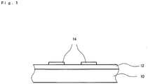
- Fig. 1 shows a partial cross sectional view of a configurational example of a substrate film of an embodiment.
- the substrate film is configured by including a base film 10, and a coating layer 12. Further, in the example of Fig. 1 , a functional thin film 14 is formed on a surface of the coating layer 12.
- the base film 10 is for example formed of polyethylene terephthalate, polyethylene naphthalate, polycarbonate, polyacrylate, polyolefin, polycycloolefin, polyimide, or paper that is processed in a film shape, however, a material thereof is not limited to these, and any material that can be used as a substrate can be used. Further, thickness of the base film 10 is not limited, and can be 10 ⁇ m to 3 mm or more,. If the thickness of the base film is too thin, such is not preferable due to a reduction in film strength, whereas on the other hand, although there is no specific limitation to the thickness being thick, a too thick base film cannot be used for cases which require flexibility. Due to this, the thickness of the film is 10 ⁇ m to 3 mm, and more preferably 16 ⁇ m to 288 ⁇ m when the flexibility and easy acquisition are taken into consideration.
- measurements of the above film thickness can for example be performed by a reflection spectroscopic film thickness meter.
- the coating layer 12 is suitably formed by a layer having a higher thermal resistance to the base film, a layer formed of a resin having a Tg (glass transition temperature) higher than 200°C. This is because resistance to heat generated upon below-described photo-sintering of the ink composite should be given.
- a crosslinked three-dimensional resin such as a polyfunctional acrylic resin is suitable, however, no limitation is made hereof; and those with a surface onto which printing can be performed by using the ink composite in which conductive particles, semiconductor particles and the like are dispersed, or lamination of metal, metal oxide and the like can be performed by sputtering and the like can be used.
- triazine thiol can be mixed in the resin configuring the coating layer 12 to improve adhesiveness to the conductor particles and the semiconductor particles.
- the thermal resistance can be improved by mixing 1 to 80 mass % of silica and/or alumina and/or titania and/or zirconia having 500 nm or less average particle diameter D50 measured by dynamic light scattering in the resin configuring the coating layer 12.
- a mixing ratio of the silica and/or alumina and/or titania and/or zirconia is small, an effect of improving the thermal resistance cannot be obtained, and if the mixing ratio is too large, coating becomes difficult.
- the mixing ratio is preferably 5 to 70 mass%, and more preferably 5 to 50 mass %.
- thickness of the coating layer 12 can be 0.1 to 10 ⁇ m.
- the coating layer 12 thinner than 0.1 ⁇ m is not preferable because such coating layer cannot function as the heat resistant layer.
- the thickness of the coating layer 12 is thicker than 10 ⁇ m, although such can be used, there may be cases in which the coating layer spoils the flexibility of a flexible base film when the coating layer is used in combination with the base film.
- the thickness of the coating layer 12 formed on the base film 10 can be measured for example by reflection spectroscopic film thickness meter FE-3000 manufactured by Taiyo Electronics Co., Ltd. by previously obtaining refractive indices of the base film 10 and the coating layer 12. In a case where the refractive indices are unknown, such may be estimated from coating amounts.
- the functional thin film 14 formed on the surface of the coating layer 12 is produced as an ink layer formed by printing the ink composite in which particles of at least one selected from the group consisting of gold, silver, copper, aluminum, nickel, cobalt, oxides thereof, graphite, graphene, carbon nanotube, zinc oxide, tin oxide, indium tin oxide, and polysilane, are dispersed in an appropriate solvent as the conductive particles.
- a conductive layer is formed by sintering this functional thin film 14 (ink layer) by the photo irradiation.
- the solvent to disperse the conductive particles for example, carbonyl compounds such as acetone, methyl ethyl ketone, cyclohexanone, benzaldehyde, octyl aldehyde and the like; ester compounds such as methyl acetate, ethyl acetate, butyl acetate, ethyl lactate, methoxyethyl acetate and the like; carboxylic acids such as formic acid, acetic acid, oxalic acid and the like; ether compounds such as diethyl ether, ethylene glycol dimethyl ether, ethyl cellosolve, butyl cellosolve, phenyl cellosolve, dioxane and the like; aromatic hydrocarbon compounds such as toluene, xylene, naphthalene, decaline and the like; aliphatic hydrocarbon compounds such as pentane, hexane, octane
- solvents water-soluble solvents are preferable, and especially alcohol and water are preferable.
- the solvent in a case of using the metal oxides as the conductive particles, it is preferable for the solvent to contain a reducing agent.
- organic solvents have reduction properties, however, in considering reduction efficiency, polyalcohol such as ethylene glycol, propylene glycol, glycerin and the like and carboxylic acids such as formic acid, acetic acid, oxalic acid and the like are suitable.
- a binder resin can be used for a purpose of adjusting viscosity and the like.
- Polymers that can be used as the binder resin may be thermoplastic resins or thermoset resins such as: poly-N-vinyl compounds such as polyvinyl-pyrrolidone, polyvinyl-caprolactone and the like, polyalkylene glycol compounds such as polyethylene glycol, polypropylene glycol, poly THF and the like, polyurethane, cellulose compounds and derivatives thereof, epoxy compounds, polyester compounds, chlorinated polyolefin, and polyacrylic compounds.
- These binder resins all have functions as reducing agents although there are differences in degrees of their effects.
- polyvinyl-pyrrolidone is preferable in considering the binder effect
- polyalkylene glycol such as polyethylene glycol, polypropylene glycol and the like is preferable in considering the reduction effect
- polyurethane compounds are preferable from the viewpoint of the adhesiveness of the binder.
- a method of printing the ink composite is not particularly limited, however, a wet coating can for example be exemplified.
- the wet coating refers to a process of producing a film by applying liquid on the coating layer 12.
- the wet coating used in the present embodiment is not particularly limited so long as it is one of the known methods; and spray coating, bar coating, roll coating, die coating, dip coating, drop coating, ink jet printing, screen printing, relief printing, intaglio printing, planographic printing, gravure printing and the like can be used.
- continuous light or pulsed light of 200 nm to 3000 nm can be used, and the pulsed light by which heat accumulation upon sintering is more unlikely to occur is more preferable.
- pulsed light refers to light having a short photo irradiation period (irradiation time), that is, in a case of repeating irradiation of pulsed light for plural times, as shown in Fig. 2 , the photo irradiation includes a period during which the light is not irradiated (irradiation interval (off)) between a first photo irradiation period (on) and a second photo irradiation period (on).
- photo intensity of the pulsed light is shown as being constant, the photo intensity can change within one photo irradiation period (on).
- the pulsed light is irradiated from a light source provided with a flash lamp such as a xenon flash lamp.
- the pulsed light is irradiated onto the layer of the ink composite by using such a light source.
- a flash lamp such as a xenon flash lamp.
- the pulsed light is irradiated onto the layer of the ink composite by using such a light source.
- one cycle (on + off) in Fig. 2 is repeated n times. Note that, in the case of repeatedly irradiating, it is preferable to perform cooling from a substrate side so that the substrate can be cooled to substantially a room temperature upon performing a subsequent pulse photo irradiation.
- One irradiation period (on) of the pulsed light has a range of 5 microseconds to 1 second, and more preferably of 20 microseconds to 10 milliseconds.
- the sintering will not progress if the period is shorter than 5 microseconds, so an effect of improving property of the conductive layer (improving conductivity) becomes low. Further, if the period is longer than 1 second, an undesired influence due to photo degradation and heat deterioration becomes greater.
- the irradiation of the pulsed light can achieve the effects with a single irradiation, the irradiation can be repeated as described above.
- the irradiation interval (off) may have a range of 20 microseconds to 5 seconds, and more preferably of 2000 microseconds to 2 seconds. If the period is shorter than 20 microseconds, the light becomes close to the continuous light and is irradiated again with hardly any interval to be cooled after the previous irradiation, so there is a possibility that the substrate is heated, whereby a temperature thereof is increased and deterioration occurs. Further, if the period is longer than 5 seconds, although the effects to some degree can be achieved because the cooling progresses in the meantime, the effect of repetitive irradiation is reduced.
- the light source that operates at or more than 0.2 Hz can be used for the irradiation of the pulsed light.
- electromagnetic waves having a wavelength range of 1 pm to 1 m can be used as the pulsed light.
- gamma ray, X-ray, ultraviolet ray, visible light, infrared ray and the like can be exemplified. Note that, in considering the conversion to thermal energy, too short wavelengths will cause larger damage to the ink layer itself, and too long wavelengths will not have an efficient absorption property which makes heat generation difficult.
- the range of the wavelength among the aforementioned wavelengths, especially the wavelength range of 10 nm to 1000 ⁇ m that is from far ultraviolet to far infrared is preferable, and the wavelength range of 200 nm to 3000 nm is more preferable.
- the functional thin film 14 a film formed by sputtering targeting silicon, germanium, tin, lead, arsenic, antimony, bismuth, gallium, indium, tallium, zinc, cadmium, selenium, tellurium, and oxides and complex oxides thereof can be used.
- the thin film itself formed by the sputtering By sintering the thin film itself formed by the sputtering, at least a part of the amorphous thin film can be crystallized; and by applying it as a semiconductor material for example for a field effect transistor, a field effect transistor having an improved charge mobility can be manufactured.
- the resin material that will be a raw material for the coating layer 12 is applied at the thickness of 0.1 to 10 ⁇ m on the surface of the base film 10 by the roll coating, bar coating, spray coating, dip coating, drop coating, die coating, spin coating and the like, to form the coating layer 12 on the base film 10.
- the ink composite is printed on the surface of the coating layer 12 of the substrate film produced according to the above by using an appropriate printing method, to form the functional thin film 14.
- the formed functional thin film 14 is sintered by the photo irradiation, to form the conductive layer (functional thin layer).
- the base film 10 can be protected from the heat generated as a result of internal heat generation caused by the photo irradiation in the conductive particles, so the generation of wrinkling or the occurrence of melting in the base film 10 can be avoided.
- Coating solution was prepared by mixing 40 parts of KAYARAD UX-5000 (pentafunctional urethane acrylate, manufactured by NIPPON KAYAKU Co., Ltd.), 60 parts of KAYARAD DPHA (mixture of dipentaerythritol pentaacrylate and dipentaerythritol hexaacrylate, manufactured by NIPPON KAYAKU Co., Ltd.), and 2 parts of Irgacure184 (1-hydroxy-cyclohexyl-phenyl-ketone, manufactured by Ciba Japan Co., Ltd.).
- KAYARAD UX-5000 manufactured by NIPPON KAYAKU Co., Ltd.
- 60 parts of KAYARAD DPHA manufactured by NIPPON KAYAKU Co., Ltd.
- 0.02 parts of AIBN azoisobutyronitrile
- Coating solution was prepared by mixing 10 parts of 3',4' - epoxycyclohexylmethyl 3,4 - epoxycyclohexane carboxylate (CELLOXIDE 2021P, manufactured by Daicel Corporation), and 0.2 parts of CPI-100P (photo-cationic curing agent, manufactured by SAN-APRO Ltd.).
- CELLOXIDE 2021P 3',4' - epoxycyclohexylmethyl 3,4 - epoxycyclohexane carboxylate
- CPI-100P photo-cationic curing agent
- Coating solution was prepared by mixing 7 parts of Ripoxy VR-77 (vinylester resin, manufactured by Showa Denko K.K.), 2 parts of cyclohexyl methacrylate, 1 part of KAYARAD DPHA (mixture of dipentaerythritol pentaacrylate and dipentaerythritol hexaacrylate, manufactured by NIPPON KAYAKU Co., Ltd.), 20 parts of methyl ethyl ketone, and 0.2 parts of Irgacure 184 (1-hydroxy-cyclohexyl-phenyl-ketone, manufactured by Ciba Japan Co., Ltd.).
- Ripoxy VR-77 vinyl resin, manufactured by Showa Denko K.K.
- 2 parts of cyclohexyl methacrylate 1 part of KAYARAD DPHA (mixture of dipentaerythritol pentaacrylate and dipentaerythritol hexaacrylate, manufactured by NIPPON KAYAKU Co., Ltd.)
- KAYARAD DPHA mixed of dipentaerythritol pentaacrylate and dipentaerythritol hexaacrylate, manufactured by NIPPON KAYAKU Co., Ltd.
- dicumyl peroxide 0.1 g of dicumyl peroxide was mixed, and cured between two glass plates at 120°C for 1hr, 140°C for 3hrs, and 160°C for 1hr. The glass transition temperature of this cured resin was confirmed to be 148°C.
- Coating solution was prepared by dissolving 10 parts of ACRYPET VH (polymethylmethacrylate, manufactured by Mitsubishi Rayon Co., Ltd.) in 50 parts of methyl ethyl ketone.
- the glass transition temperature was measured under the following conditions.
- thermomechaical analysis TMA
- TMA/SS6100 manufactured by SII Nano Technology Inc. was used to perform measurement of a sample of 9 ⁇ 9 ⁇ 3 mm under the conditions that the temperature ranges from -10 to 300°C, the rate of temperature rise is 5°C /min, and the load is 20.0 mN.
- the temperature at the intersection of two lines respectively extrapolated from linear regions located below and above the inflection point was determined as the glass transition temperature.
- particle diameters of the particles were measured by Nanotrac UPA-EX150 (dynamic light scattering), the particle diameters were calculated by spherical approximation, and the median diameter D50 was obtained.
- the coating solution prepared in Reference Example 1 was coated on Lumirror 125U98 (polyethylene-terephthalate film manufactured by TORAY INDUSTRIES, INC.) that is a base film, irradiation of 100 mj/cm 2 by a high-pressure mercury UV lamp was performed thereto for curing, and thereby, a heat resistant layer having a thickness of 5 ⁇ m was formed.
- the paste obtained in Reference Example 5 was used to screen print a pattern of 2 cm ⁇ 2 cm square on this heat resistant layer. Pulsed photo irradiation was performed on a paste-printed surface side of the obtained sample by using Sinteron3300 manufactured by Xenon corporation.
- the irradiation conditions were single irradiation with pulse width of 2000 microseconds, voltage of 3000V, and irradiation distance of 20 cm. Pulse energy upon that occasion was 2070 J. Thickness of a conductive film formed in accordance with the above was 25 ⁇ m. Note that, the series of the above procedures were carried out under air atmosphere.
- the volume resistivity of the obtained film was 8.7 ⁇ 10 -5 ⁇ cm, and that transition to the conductive film was performed by photo-sintering.
- Fig. 4 shows a picture of the pattern forming surface after the photo irradiation.
- portions with wrinkling and melting were not generated in the base film, and no damage caused by the photo irradiation was recognized in the base film.
- the coating solution prepared in Reference Example 2 was used, but aside from the aforementioned, similar operations as those of Example 1 were performed.
- the obtained conductive film had a thickness of 22 ⁇ m, and a volume resistivity of 9.6 ⁇ 10 -5 ⁇ cm.
- the coating solution prepared in Reference Example 3 was used, and COSMO SHINE A4300 (polyethylene terephthalate film, manufactured by Toyobo Co., Ltd.) was used as a base film, but aside from the aforementioned, similar operations as those of the Example 1 were performed.
- the obtained conductive film had a thickness of 23 ⁇ m, and a volume resistivity of 4.2 ⁇ 10 -5 ⁇ cm.
- the coating layer was not formed on Lumirror 125U98 (polyethylene terephthalate film manufactured by TORAY INDUSTRIES, INC.), and the paste obtained in the Reference Example 2 was directly screen printed on Lumirror 125U98, but aside from the aforementioned, similar operations as those of the Example 1 were performed.
- Fig. 5 shows a picture of the pattern forming surface after the photo irradiation in the same manner as Example 1.
- a part of the printed pattern was blown up, and a part of the base film (PET film) had melted.
- the coating solution prepared in Reference Example 4 was used, but aside from the aforementioned, similar operations as those of Example 1 were performed. As a result, a part of the printed pattern was blown up, and a part of the base film (PET film) had melted.
- the coating solution prepared in Reference Example 1 was coated on Lumirror 125U98 (polyethylene-terephthalate film manufactured by TORAY INDUSTRIES INC.) that is the base film, irradiation of 100 mj/cm 2 by the high-pressure mercury UV lamp was performed thereto for curing, and thereby, the heat resistant layer having a thickness of 5 ⁇ m was formed. Silicon was deposited by sputtering on this heat resistant layer so as to have a thickness of 200 nm.
- Lumirror 125U98 polyethylene-terephthalate film manufactured by TORAY INDUSTRIES INC.
- Example 4 Other than having deposited silicon without forming the coating layer on Lumirror 125U98 (polyethylene-terephthalate film manufactured by TORAY INDUSTRIES INC.), similar operations as those of Example 4 were performed.
Description
- The present invention relates to a substrate film and a sintering method.
- To form a conductive layer such as a semiconductor, metal and the like on a substrate, for example, the conductive layer may be formed by printing an ink layer on the substrate using an ink composite (conductive ink) in which conductive particles are dispersed, and sintering the conductive particles in the ink layer.
- For example, the below described
Patent Document 1 discloses a technique that coats an adhering layer by applying an adhesive to a substrate, coats a water repellent layer on the substrate on which the adhering layer is coated, prints conductive ink on the substrate on which the adhering layer and the water repellent layer are coated, and performs sintering of the printed conductive ink and curing of the adhering layer. - Further, the below described Patent Document 2 discloses a device that manufactures an electronic component by scattering metal microparticles on a substrate including an insulating pattern formed by a thermoset resin to adhere the metal microparticles on the insulating pattern, melting the insulating pattern by heating, fixing the metal microparticles on the insulating pattern, and removing the metal microparticles adhered to a surface of the substrate other than the insulating pattern.
- In the method of
Patent Document 1, a sintering condition is heating for 1 hour at 200°C (paragraph 0044 of Patent Document 1), and in the method of Patent Document 2, a heating temperature of the insulating pattern is 150 to 200°C (paragraph 0028 and the like of Patent Document 2), however, generally, upon heating a conductive pattern or an insulating pattern on a substrate, the heating is performed on an entire substrate; thus, the substrate that can be used is limited to those with high heat resistivity, such as substrates made of a thermoset resin with a high thermal resistance, for example, a BT resin including bismaleimide-triazine compounds and the like. - Due to this, as described in Patent Documents 3 to 5, there had been attempts to use an ink composite including nanoparticles, and form a metal pattern from the ink composite by photo irradiation. Methods that use light energy or microwaves in heating can selectively heat only the ink composite (nanoparticles), and there is a possibility that a resin having a lower thermal resistance than the above described resin can be used as the substrate.
-
- [Patent Document 1] Japanese Patent Application Laid-Open No.
2010-75911 - [Patent Document 2] Japanese Patent Application Laid-Open No.
2005-203396 - [Patent Document 3] Japanese Patent Application National Publication No.
2008-522369 - [Patent Document 4]
WO 2010/110969 - [Patent Document 5] Japanese Patent Application National Publication No.
2010-528428 - However, in a case of using an ink composite in which silicon particles or nickel oxide particles are for example dispersed, energy of light to be irradiated needs to be increased because energy is required for transition of a crystal structure of the silicon particles or reduction of nickel oxides. Further, also in a case of forming a thick conductive layer by using an ink composite in which copper particles or copper oxide particles are dispersed, the energy of the light to be irradiated needs to be increased because more energy is required than in forming a thin film. Due to this, when a resin with a low thermal resistance such as PET and the like is used for the substrate, there were problems in that wrinkling or melting occurs in the substrate during sintering of the ink composite.
- Further relevant background art is disclosed in documents
US 2006/257625 A1 ,US 2010/059251 A1 ,US 6 251 507 B1 andUS 2008/020304 A1 . - An objective of the present invention is to provide a substrate film and a sintering method capable of preventing the occurrence of wrinkling, melting and the like in a substrate during photo irradiation.
- In order to achieve the above objective, one aspect of the present invention is a substrate film comprising a base film, and a coating layer (heat resistant layer) formed on the base film, wherein the coating layer is formed of a heat resistant resin having a higher Tg than the base film, and has a surface on which a functional thin film is to be sintered by photo irradiation. The heat resistant resin has a Tg (glass transition temperature) higher than 200°C.
- The resin that forms the coating layer can be a crosslinked three-dimensional resin. Thickness of the coating layer may be 0.1 to 10 µm.
- Further, the heat resistant resin that forms the coating layer can contain 5 to 80 mass % of at least one filler selected from the group consisting of silica, alumina, titania and zirconia, the filler having 500 nm or less average particle diameter d50 measured by dynamic light scattering.
- Further, the base film can be a polyethylene terephthalate film, polyethylene naphthalate film, polycarbonate film, polyacrylate film, polyolefin film, polycycloolefin film, or polyimide film, or paper. Thickness of the base film can be 10 µm to 3 mm.
- Further, another aspect of the present invention is a substrate provided with a functional thin layer (pattern) which is sintered by photo irradiation on the coating layer (heat resistant layer) of the above mentioned respective substrate films.
- Further, another aspect of the present invention is a sintering method comprising preparing the respective substrate films, forming the functional thin film (pattern) on the surface of the coating layer, and sintering the functional thin film (pattern) by the photo irradiation.
- The light to be irradiated can be pulsed light having a wavelength of 200 to 3000 nm.
- The functional thin film (pattern) may comprises at least one selected from the group consisting of gold, silver, copper, aluminum, nickel, cobalt, oxides thereof, graphite, graphene, carbon nanotube, zinc oxide, tin oxide, indium tin oxide, and polysilane.
- Further, the functional thin film (pattern) can be formed by sputtering targeting silicon, germanium, tin, lead, arsenic, antimony, bismuth, gallium, indium, tallium, zinc, cadmium, selenium, tellurium, and oxides and complex oxides thereof.
-
-
Fig. 1 is a partial cross sectional view of a configurational example of a substrate film of an embodiment. -
Fig. 2 is a diagram for explaining a definition of pulsed light. -
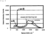
Fig. 3 is a Raman spectrum showing that a change in a crystal structure of silicon has occurred by photo irradiation in Example 2. -
Fig. 4 is a picture showing a pattern forming surface after photo irradiation in Example 1. -
Fig. 5 is a picture showing a pattern forming surface after photo irradiation in Comparative Example 1. - Hereinbelow, exemplary embodiments (hereinbelow referred to as embodiments) will be explained with reference to the drawings.
-
Fig. 1 shows a partial cross sectional view of a configurational example of a substrate film of an embodiment. InFig. 1 , the substrate film is configured by including abase film 10, and acoating layer 12. Further, in the example ofFig. 1 , a functionalthin film 14 is formed on a surface of thecoating layer 12. - The
base film 10 is for example formed of polyethylene terephthalate, polyethylene naphthalate, polycarbonate, polyacrylate, polyolefin, polycycloolefin, polyimide, or paper that is processed in a film shape, however, a material thereof is not limited to these, and any material that can be used as a substrate can be used. Further, thickness of thebase film 10 is not limited, and can be 10 µm to 3 mm or more,. If the thickness of the base film is too thin, such is not preferable due to a reduction in film strength, whereas on the other hand, although there is no specific limitation to the thickness being thick, a too thick base film cannot be used for cases which require flexibility. Due to this, the thickness of the film is 10µm to 3 mm, and more preferably 16 µm to 288 µm when the flexibility and easy acquisition are taken into consideration. - Note that, measurements of the above film thickness can for example be performed by a reflection spectroscopic film thickness meter.
- The
coating layer 12 is suitably formed by a layer having a higher thermal resistance to the base film, a layer formed of a resin having a Tg (glass transition temperature) higher than 200°C. This is because resistance to heat generated upon below-described photo-sintering of the ink composite should be given. As a material configuring thecoating layer 12, a crosslinked three-dimensional resin such as a polyfunctional acrylic resin is suitable, however, no limitation is made hereof; and those with a surface onto which printing can be performed by using the ink composite in which conductive particles, semiconductor particles and the like are dispersed, or lamination of metal, metal oxide and the like can be performed by sputtering and the like can be used. Further, triazine thiol can be mixed in the resin configuring thecoating layer 12 to improve adhesiveness to the conductor particles and the semiconductor particles. Further, the thermal resistance can be improved by mixing 1 to 80 mass % of silica and/or alumina and/or titania and/or zirconia having 500 nm or less average particle diameter D50 measured by dynamic light scattering in the resin configuring thecoating layer 12. Here, if a mixing ratio of the silica and/or alumina and/or titania and/or zirconia is small, an effect of improving the thermal resistance cannot be obtained, and if the mixing ratio is too large, coating becomes difficult. The mixing ratio is preferably 5 to 70 mass%, and more preferably 5 to 50 mass %. - Further, thickness of the
coating layer 12 can be 0.1 to 10 µm. Thecoating layer 12 thinner than 0.1 µm is not preferable because such coating layer cannot function as the heat resistant layer. Whereas on the other hand, if the thickness of thecoating layer 12 is thicker than 10 µm, although such can be used, there may be cases in which the coating layer spoils the flexibility of a flexible base film when the coating layer is used in combination with the base film. - The thickness of the
coating layer 12 formed on thebase film 10 can be measured for example by reflection spectroscopic film thickness meter FE-3000 manufactured by Taiyo Electronics Co., Ltd. by previously obtaining refractive indices of thebase film 10 and thecoating layer 12. In a case where the refractive indices are unknown, such may be estimated from coating amounts. - By having the configuration of the substrate film of the present embodiment, occurrence of wrinkling, melting and the like in the substrate caused during the irradiation of light can effectively be suppressed in cases of using a base film with a relatively low thermal resistance such as polyethylene-terephthalate, however, this does not exclude uses of polyimide film and the like having a relatively high thermal resistance as the
base film 10. - The functional
thin film 14 formed on the surface of thecoating layer 12 is produced as an ink layer formed by printing the ink composite in which particles of at least one selected from the group consisting of gold, silver, copper, aluminum, nickel, cobalt, oxides thereof, graphite, graphene, carbon nanotube, zinc oxide, tin oxide, indium tin oxide, and polysilane, are dispersed in an appropriate solvent as the conductive particles. Note that, a conductive layer is formed by sintering this functional thin film 14 (ink layer) by the photo irradiation. - As the solvent to disperse the conductive particles, for example, carbonyl compounds such as acetone, methyl ethyl ketone, cyclohexanone, benzaldehyde, octyl aldehyde and the like; ester compounds such as methyl acetate, ethyl acetate, butyl acetate, ethyl lactate, methoxyethyl acetate and the like; carboxylic acids such as formic acid, acetic acid, oxalic acid and the like; ether compounds such as diethyl ether, ethylene glycol dimethyl ether, ethyl cellosolve, butyl cellosolve, phenyl cellosolve, dioxane and the like; aromatic hydrocarbon compounds such as toluene, xylene, naphthalene, decaline and the like; aliphatic hydrocarbon compounds such as pentane, hexane, octane and the like; halogen hydrocarbons such as methylene chloride, chlorobenzene, chloroform and the like; alcohol-based compounds such as methanol, ethanol, n-propanol, isopropanol, butanol, cyclohexanol, terpineol, ethylene glycol, propylene glycol, glycerin and the like; water; and mixed solvents thereof may be exemplified. Among the above solvents, water-soluble solvents are preferable, and especially alcohol and water are preferable. Note that, in a case of using the metal oxides as the conductive particles, it is preferable for the solvent to contain a reducing agent. Although the above mentioned organic solvents have reduction properties, however, in considering reduction efficiency, polyalcohol such as ethylene glycol, propylene glycol, glycerin and the like and carboxylic acids such as formic acid, acetic acid, oxalic acid and the like are suitable.
- Further, in order to print the ink composite, a binder resin can be used for a purpose of adjusting viscosity and the like. Polymers that can be used as the binder resin may be thermoplastic resins or thermoset resins such as: poly-N-vinyl compounds such as polyvinyl-pyrrolidone, polyvinyl-caprolactone and the like, polyalkylene glycol compounds such as polyethylene glycol, polypropylene glycol, poly THF and the like, polyurethane, cellulose compounds and derivatives thereof, epoxy compounds, polyester compounds, chlorinated polyolefin, and polyacrylic compounds. These binder resins all have functions as reducing agents although there are differences in degrees of their effects. Among these, polyvinyl-pyrrolidone is preferable in considering the binder effect, polyalkylene glycol such as polyethylene glycol, polypropylene glycol and the like is preferable in considering the reduction effect, and further, polyurethane compounds are preferable from the viewpoint of the adhesiveness of the binder.
- A method of printing the ink composite is not particularly limited, however, a wet coating can for example be exemplified. The wet coating refers to a process of producing a film by applying liquid on the
coating layer 12. The wet coating used in the present embodiment is not particularly limited so long as it is one of the known methods; and spray coating, bar coating, roll coating, die coating, dip coating, drop coating, ink jet printing, screen printing, relief printing, intaglio printing, planographic printing, gravure printing and the like can be used. - As the light used in the above sintering, continuous light or pulsed light of 200 nm to 3000 nm can be used, and the pulsed light by which heat accumulation upon sintering is more unlikely to occur is more preferable.
- In the present description, "pulsed light" refers to light having a short photo irradiation period (irradiation time), that is, in a case of repeating irradiation of pulsed light for plural times, as shown in
Fig. 2 , the photo irradiation includes a period during which the light is not irradiated (irradiation interval (off)) between a first photo irradiation period (on) and a second photo irradiation period (on). InFig. 2 , although photo intensity of the pulsed light is shown as being constant, the photo intensity can change within one photo irradiation period (on). The pulsed light is irradiated from a light source provided with a flash lamp such as a xenon flash lamp. The pulsed light is irradiated onto the layer of the ink composite by using such a light source. In a case of repeating n times of irradiations, one cycle (on + off) inFig. 2 is repeated n times. Note that, in the case of repeatedly irradiating, it is preferable to perform cooling from a substrate side so that the substrate can be cooled to substantially a room temperature upon performing a subsequent pulse photo irradiation. - One irradiation period (on) of the pulsed light has a range of 5 microseconds to 1 second, and more preferably of 20 microseconds to 10 milliseconds. The sintering will not progress if the period is shorter than 5 microseconds, so an effect of improving property of the conductive layer (improving conductivity) becomes low. Further, if the period is longer than 1 second, an undesired influence due to photo degradation and heat deterioration becomes greater. Although the irradiation of the pulsed light can achieve the effects with a single irradiation, the irradiation can be repeated as described above. In the case of repeatedly irradiating, the irradiation interval (off) may have a range of 20 microseconds to 5 seconds, and more preferably of 2000 microseconds to 2 seconds. If the period is shorter than 20 microseconds, the light becomes close to the continuous light and is irradiated again with hardly any interval to be cooled after the previous irradiation, so there is a possibility that the substrate is heated, whereby a temperature thereof is increased and deterioration occurs. Further, if the period is longer than 5 seconds, although the effects to some degree can be achieved because the cooling progresses in the meantime, the effect of repetitive irradiation is reduced. Note that, the light source that operates at or more than 0.2 Hz can be used for the irradiation of the pulsed light. Further, electromagnetic waves having a wavelength range of 1 pm to 1 m can be used as the pulsed light. As an example of such electromagnetic waves, gamma ray, X-ray, ultraviolet ray, visible light, infrared ray and the like can be exemplified. Note that, in considering the conversion to thermal energy, too short wavelengths will cause larger damage to the ink layer itself, and too long wavelengths will not have an efficient absorption property which makes heat generation difficult. Accordingly, as the range of the wavelength, among the aforementioned wavelengths, especially the wavelength range of 10 nm to 1000 µm that is from far ultraviolet to far infrared is preferable, and the wavelength range of 200 nm to 3000 nm is more preferable.
- Further, as the functional
thin film 14, a film formed by sputtering targeting silicon, germanium, tin, lead, arsenic, antimony, bismuth, gallium, indium, tallium, zinc, cadmium, selenium, tellurium, and oxides and complex oxides thereof can be used. - By sintering the thin film itself formed by the sputtering, at least a part of the amorphous thin film can be crystallized; and by applying it as a semiconductor material for example for a field effect transistor, a field effect transistor having an improved charge mobility can be manufactured.
- In the case of manufacturing the substrate film of the present embodiment, the resin material that will be a raw material for the
coating layer 12 is applied at the thickness of 0.1 to 10 µm on the surface of thebase film 10 by the roll coating, bar coating, spray coating, dip coating, drop coating, die coating, spin coating and the like, to form thecoating layer 12 on thebase film 10. The ink composite is printed on the surface of thecoating layer 12 of the substrate film produced according to the above by using an appropriate printing method, to form the functionalthin film 14. Next, the formed functionalthin film 14 is sintered by the photo irradiation, to form the conductive layer (functional thin layer). At this occasion, since thecoating layer 12 has the thermal resistance, thebase film 10 can be protected from the heat generated as a result of internal heat generation caused by the photo irradiation in the conductive particles, so the generation of wrinkling or the occurrence of melting in thebase film 10 can be avoided. - Hereinbelow, Examples of the present invention will specifically be explained. Note that, the following Examples are provided for the sake of easy understanding of the present invention, and the present invention is not to be limited to these Examples.
- Coating solution was prepared by mixing 40 parts of KAYARAD UX-5000 (pentafunctional urethane acrylate, manufactured by NIPPON KAYAKU Co., Ltd.), 60 parts of KAYARAD DPHA (mixture of dipentaerythritol pentaacrylate and dipentaerythritol hexaacrylate, manufactured by NIPPON KAYAKU Co., Ltd.), and 2 parts of Irgacure184 (1-hydroxy-cyclohexyl-phenyl-ketone, manufactured by Ciba Japan Co., Ltd.).
- Further, aside from the above, 40 parts of KAYARAD UX-5000 (manufactured by NIPPON KAYAKU Co., Ltd.), 60 parts of KAYARAD DPHA(manufactured by NIPPON KAYAKU Co., Ltd.), and 0.02 parts of AIBN (azoisobutyronitrile) were mixed, and cured between two glass plates at 40°C for 1hr, 60°C for 3hrs, and 120°C for 1hr. The glass transition temperature of this cured resin was confirmed to be 259°C.
- Coating solution was prepared by mixing 10 parts of 3',4' - epoxycyclohexylmethyl 3,4 - epoxycyclohexane carboxylate (CELLOXIDE 2021P, manufactured by Daicel Corporation), and 0.2 parts of CPI-100P (photo-cationic curing agent, manufactured by SAN-APRO Ltd.).
- Further, aside from the above, 10 parts of CELLOXIDE 2021P, and 0.2 parts of San-Aid SI-100L (thermal cationic curing agent, manufactured by Sanshin Chemical Industry Co., Ltd.) were mixed, and cured between two glass plates at 100°C for 1hr, 120 C°for 3hrs, 160°C for 1 hr. The glass transition temperature of this cured resin was confirmed to be 178°C.
- Coating solution was prepared by mixing 7 parts of Ripoxy VR-77 (vinylester resin, manufactured by Showa Denko K.K.), 2 parts of cyclohexyl methacrylate, 1 part of KAYARAD DPHA (mixture of dipentaerythritol pentaacrylate and dipentaerythritol hexaacrylate, manufactured by NIPPON KAYAKU Co., Ltd.), 20 parts of methyl ethyl ketone, and 0.2 parts of Irgacure 184 (1-hydroxy-cyclohexyl-phenyl-ketone, manufactured by Ciba Japan Co., Ltd.).
- Further, aside from the above, 7 parts of Ripoxy VR-77 (vinylester resin, manufactured by Showa Denko K.K.), 2 parts of cyclohexyl methacrylate, 1 part of KAYARAD DPHA (mixture of dipentaerythritol pentaacrylate and dipentaerythritol hexaacrylate, manufactured by NIPPON KAYAKU Co., Ltd.), and 0.1 g of dicumyl peroxide were mixed, and cured between two glass plates at 120°C for 1hr, 140°C for 3hrs, and 160°C for 1hr. The glass transition temperature of this cured resin was confirmed to be 148°C.
- Coating solution was prepared by dissolving 10 parts of ACRYPET VH (polymethylmethacrylate, manufactured by Mitsubishi Rayon Co., Ltd.) in 50 parts of methyl ethyl ketone.
- Further, aside from the above, a glass transition temperature of ACRYPET VH was measured, and was confirmed to be 106°C.
- The glass transition temperature was measured under the following conditions.
- The measurement was performed by a thermomechaical analysis (TMA). A thermomechanical analyser TMA/SS6100 manufactured by SII Nano Technology Inc. was used to perform measurement of a sample of 9 × 9 × 3 mm under the conditions that the temperature ranges from -10 to 300°C, the rate of temperature rise is 5°C /min, and the load is 20.0 mN. In the obtained expansion curve showing temperature transition, the temperature at the intersection of two lines respectively extrapolated from linear regions located below and above the inflection point was determined as the glass transition temperature.
- Binder solution of 40 mass % was prepared by dissolving polyvinylpyrrolidone (manufactured by NIPPON SHOKUBAI CO., LTD.) as a binder in mixed aqueous solution of ethylene glycol and glycerin (reagent grade manufactured by KANTO CHEMICAL CO., INC.) (mass ratio of ethylene glycol: glycerin : water = 70 : 15 : 15) as a reducing agent. 1.5 g of this binder solution and 0.5 g of the mixed aqueous solution were mixed, 6.0 g of NanoTek CuO (spherical shaped, D50 = 270 nm) manufactured by C. I. KASEI CO., LTD. was mixed therein as copper oxide particles, the resulting mixture was well mixed by a planetary centrifugal vacuum mixer "Thinky Mixer" ARV-310 (Awatori Rentaro) (manufactured by THINKY CORPORATION), and a paste for printing (composition for forming a conductive film) was produced thereby.
- Note that, particle diameters of the particles were measured by Nanotrac UPA-EX150 (dynamic light scattering), the particle diameters were calculated by spherical approximation, and the median diameter D50 was obtained.
- The coating solution prepared in Reference Example 1 was coated on Lumirror 125U98 (polyethylene-terephthalate film manufactured by TORAY INDUSTRIES, INC.) that is a base film, irradiation of 100 mj/cm2 by a high-pressure mercury UV lamp was performed thereto for curing, and thereby, a heat resistant layer having a thickness of 5 µm was formed. The paste obtained in Reference Example 5 was used to screen print a pattern of 2 cm × 2 cm square on this heat resistant layer. Pulsed photo irradiation was performed on a paste-printed surface side of the obtained sample by using Sinteron3300 manufactured by Xenon corporation. The irradiation conditions were single irradiation with pulse width of 2000 microseconds, voltage of 3000V, and irradiation distance of 20 cm. Pulse energy upon that occasion was 2070 J. Thickness of a conductive film formed in accordance with the above was 25 µm. Note that, the series of the above procedures were carried out under air atmosphere.
- It had been confirmed that the volume resistivity of the obtained film was 8.7 × 10⁻⁵ Ω·cm, and that transition to the conductive film was performed by photo-sintering.
-
Fig. 4 shows a picture of the pattern forming surface after the photo irradiation. InFig. 4 , portions with wrinkling and melting were not generated in the base film, and no damage caused by the photo irradiation was recognized in the base film. - The coating solution prepared in Reference Example 2 was used, but aside from the aforementioned, similar operations as those of Example 1 were performed. The obtained conductive film had a thickness of 22 µm, and a volume resistivity of 9.6 × 10⁻⁵ Ω·cm.
- The coating solution prepared in Reference Example 3 was used, and COSMO SHINE A4300 (polyethylene terephthalate film, manufactured by Toyobo Co., Ltd.) was used as a base film, but aside from the aforementioned, similar operations as those of the Example 1 were performed. The obtained conductive film had a thickness of 23 µm, and a volume resistivity of 4.2 × 10⁻⁵ Ω·cm.
- The coating layer was not formed on Lumirror 125U98 (polyethylene terephthalate film manufactured by TORAY INDUSTRIES, INC.), and the paste obtained in the Reference Example 2 was directly screen printed on Lumirror 125U98, but aside from the aforementioned, similar operations as those of the Example 1 were performed.
-
Fig. 5 shows a picture of the pattern forming surface after the photo irradiation in the same manner as Example 1. InFig. 5 , a part of the printed pattern was blown up, and a part of the base film (PET film) had melted. - The coating solution prepared in Reference Example 4 was used, but aside from the aforementioned, similar operations as those of Example 1 were performed. As a result, a part of the printed pattern was blown up, and a part of the base film (PET film) had melted.
- Similar to Example 1, the coating solution prepared in Reference Example 1 was coated on Lumirror 125U98 (polyethylene-terephthalate film manufactured by TORAY INDUSTRIES INC.) that is the base film, irradiation of 100 mj/cm2 by the high-pressure mercury UV lamp was performed thereto for curing, and thereby, the heat resistant layer having a thickness of 5 µm was formed. Silicon was deposited by sputtering on this heat resistant layer so as to have a thickness of 200 nm.
- Single photo irradiation was performed on a silicon-deposited surface side of the obtained sample by using PulseForge3300 manufactured by Novacentrix Corporation with a voltage of 350V and a pulse width of 2000 microseconds.
- As a result of having measured Raman spectrum of the silicon film of the obtained sample (
Fig. 3 ), a peak was observed at 500 cm-1. Due to this, it has been discovered that the amorphous silicon film formed by deposition had been transferred to a microcrystal silicon film by having performed the photo irradiation thereon. No abnormality caused by the photo irradiation was found in the base film (Lumirror 125U98). - Other than having deposited silicon without forming the coating layer on Lumirror 125U98 (polyethylene-terephthalate film manufactured by TORAY INDUSTRIES INC.), similar operations as those of Example 4 were performed.
- Although a peak was observed at 500 cm-1 in the Raman spectrum, similar to Example 4, deformation caused by heat upon the photo irradiation occurred in the base film (Lumirror 125U98).
- 10 base film, 12 coating layer, 14 functional thin film
Claims (13)
- A substrate film for photo irradiation, comprisinga base film (10), anda coating layer (12) formed on the base film, wherein the coating layer is formed of a heat resistant resin having a higher glass transition temperature than the base film and a glass transition temperature of higher than 200°C.
- A substrate film according to claim 1, wherein the heat resistant resin that forms the coating layer is a crosslinked three-dimensional resin.
- A substrate film according to claim 1 or 2, wherein the heat resistant resin that forms the coating layer contains 5 to 80 mass % of at least one filler selected from the group consisting of silica, alumina, titania and zirconia, the filler having 500 nm or less average particle diameter d50 measured by dynamic light scattering.
- A substrate film according to any one of claims 1 to 3, wherein the base film is a polyethylene terephthalate film, polyethylene naphthalate film, polycarbonate film, polyacrylate film, polyolefin film, polycycloolefin film, or polyimide film, or paper.
- A substrate film according to any one of claims 1 to 4, wherein the coating layer has a thickness of 0.1 to 10 µm.
- A substrate film according to any one of claims 1 to 5, wherein the base film has a thickness of 10 µm to 3 mm.
- A substrate comprising the substrate film according to any one of claims 1 to 6 and a functional thin layer (14) obtainable by sintering by photo irradiation on the coating layer (12), wherein the photo irradiation is pulsed light irradiation using a pulsed light having a wavelength of 200 to 3000 nm.
- A substrate according to claim 7, wherein the functional thin layer comprises at least one selected from the group consisting of gold, silver, copper, aluminum, nickel, cobalt, oxides thereof, graphite, graphene, carbon nanotube, zinc oxide, tin oxide, indium tin oxide, and polysilane.
- A substrate according to claim 7, wherein the functional thin layer comprises at least one selected from the group consisting of silicon, germanium, tin, lead, arsenic, antimony, bismuth, gallium, indium, tallium, zinc, cadmium, selenium, tellurium, and oxides and complex oxides thereof.
- A sintering method comprisingpreparing a substrate film according to any one of claims 1 to 6,forming a functional thin film (14) on the surface of the coating layer (12), andsintering the functional thin film by photo irradiation.
- A sintering method according to claim 10, wherein the light to be irradiated is pulsed light having a wavelength of 200 to 3000 nm.
- A sintering method according to claim 10 or 11, wherein the functional thin film is produced by printing an ink composite containing at least one selected from the group consisting of gold, silver, copper, aluminum, nickel, cobalt, oxides thereof, graphite, graphene, carbon nanotube, zinc oxide, tin oxide, indium tin oxide, and polysilane.
- A sintering method according to claim 10 or 11, wherein the functional thin film is formed by sputtering targeting silicon, germanium, tin, lead, arsenic, antimony, bismuth, gallium, indium, tallium, zinc, cadmium, selenium, tellurium, and oxides and complex oxides thereof.
Applications Claiming Priority (2)
| Application Number | Priority Date | Filing Date | Title |
|---|---|---|---|
| US201261655644P | 2012-06-05 | 2012-06-05 | |
| PCT/IB2013/001254 WO2013182896A1 (en) | 2012-06-05 | 2013-05-31 | Substrate film and sintering method |
Publications (3)
| Publication Number | Publication Date |
|---|---|
| EP2855148A1 EP2855148A1 (en) | 2015-04-08 |
| EP2855148A4 EP2855148A4 (en) | 2016-01-20 |
| EP2855148B1 true EP2855148B1 (en) | 2019-04-10 |
Family
ID=49711481
Family Applications (1)
| Application Number | Title | Priority Date | Filing Date |
|---|---|---|---|
| EP13799914.0A Active EP2855148B1 (en) | 2012-06-05 | 2013-05-31 | Substrate film and sintering method |
Country Status (6)
| Country | Link |
|---|---|
| US (1) | US9631283B2 (en) |
| EP (1) | EP2855148B1 (en) |
| JP (1) | JP6258303B2 (en) |
| KR (3) | KR20150016552A (en) |
| CN (1) | CN104797419B (en) |
| WO (1) | WO2013182896A1 (en) |
Families Citing this family (18)
| Publication number | Priority date | Publication date | Assignee | Title |
|---|---|---|---|---|
| US10000965B2 (en) | 2010-01-16 | 2018-06-19 | Cardinal Cg Company | Insulating glass unit transparent conductive coating technology |
| US10060180B2 (en) | 2010-01-16 | 2018-08-28 | Cardinal Cg Company | Flash-treated indium tin oxide coatings, production methods, and insulating glass unit transparent conductive coating technology |
| US10000411B2 (en) | 2010-01-16 | 2018-06-19 | Cardinal Cg Company | Insulating glass unit transparent conductivity and low emissivity coating technology |
| JP5275498B1 (en) * | 2012-07-03 | 2013-08-28 | 石原薬品株式会社 | Conductive film forming method and sintering promoter |
| WO2014156844A1 (en) * | 2013-03-29 | 2014-10-02 | 太陽ホールディングス株式会社 | Thermoplastic resin film base for optical firing, conductive circuit board using same, and method for manufacturing said conductive circuit board |
| EP3122542B1 (en) * | 2014-03-28 | 2019-06-05 | Ez Print, LLC | 3d print bed having permanent coating |
| CN108353503B (en) * | 2015-10-26 | 2021-02-19 | 韩国机械研究院 | Pattern forming apparatus and method using intense pulsed light sintering |
| WO2017110618A1 (en) * | 2015-12-24 | 2017-06-29 | 株式会社村田製作所 | Resin sheet, method for manufacturing resin sheet, and method for manufacturing multilayer resin substrate |
| JP2017216303A (en) * | 2016-05-30 | 2017-12-07 | 株式会社リコー | Base material for circuit member, circuit member, method of producing base material for circuit member, and method of producing circuit member |
| EP3543214A4 (en) * | 2016-11-17 | 2019-11-27 | Nippon Chemical Industrial Co., Ltd. | Cuprous oxide particles, production method therefor, photosintering composition, conductive film production method using same, and cuprous oxide particle paste |
| CN109426397B (en) * | 2017-08-22 | 2020-08-04 | 京东方科技集团股份有限公司 | Preparation method of touch structure and touch structure |
| US11028012B2 (en) | 2018-10-31 | 2021-06-08 | Cardinal Cg Company | Low solar heat gain coatings, laminated glass assemblies, and methods of producing same |
| US11267763B2 (en) | 2019-05-17 | 2022-03-08 | Raytheon Technologies Corporation | Rapid processing of laminar composite components |
| DE102019114806A1 (en) * | 2019-06-03 | 2020-12-03 | Value & Intellectual Properties Management Gmbh | Process for the production of electrical or electronic components or circuits on a flexible flat carrier |
| US20220279658A1 (en) * | 2019-07-31 | 2022-09-01 | Fuji Corporation | Method for manufacturing circuit wiring by three-dimensional additive manufacturing |
| JPWO2021044986A1 (en) * | 2019-09-05 | 2021-03-11 | ||
| CN110577771A (en) * | 2019-09-17 | 2019-12-17 | 宁波石墨烯创新中心有限公司 | conductive ink, RFID antenna, electronic tag and preparation method |
| EP4274391A1 (en) | 2022-05-06 | 2023-11-08 | Ecole Polytechnique Federale De Lausanne (Epfl) | Method for manufacturing an electrically conductive metal trace and corresponding metal trace, particularly suitable for transient electronic devices |
Family Cites Families (18)
| Publication number | Priority date | Publication date | Assignee | Title |
|---|---|---|---|---|
| JP4147639B2 (en) | 1998-09-29 | 2008-09-10 | 宇部興産株式会社 | Flexible metal foil laminate |
| US7394663B2 (en) * | 2003-02-18 | 2008-07-01 | Matsushita Electric Industrial Co., Ltd. | Electronic component built-in module and method of manufacturing the same |
| US20060257625A1 (en) | 2003-09-10 | 2006-11-16 | Yasuhiro Wakizaka | Resin composite film |
| JP2005203396A (en) | 2004-01-13 | 2005-07-28 | Toshiba Corp | Electronic component and method and apparatus for manufacturing the same |
| CA2588343C (en) | 2004-11-24 | 2011-11-08 | Nanotechnologies, Inc. | Electrical, plating and catalytic uses of metal nanomaterial compositions |
| US8945686B2 (en) | 2007-05-24 | 2015-02-03 | Ncc | Method for reducing thin films on low temperature substrates |
| US8133592B2 (en) | 2007-02-14 | 2012-03-13 | Toray Industries, Inc. | Laminated adhesive thermoplastic resin film |
| US10231344B2 (en) | 2007-05-18 | 2019-03-12 | Applied Nanotech Holdings, Inc. | Metallic ink |
| CN101795865B (en) | 2007-07-31 | 2013-12-04 | 大科能树脂有限公司 | Layered product |
| US7833683B2 (en) * | 2007-08-14 | 2010-11-16 | Xerox Corporation | Photosensitive member having an overcoat |
| US8410712B2 (en) | 2008-07-09 | 2013-04-02 | Ncc Nano, Llc | Method and apparatus for curing thin films on low-temperature substrates at high speeds |
| KR100999506B1 (en) * | 2008-09-09 | 2010-12-09 | 삼성전기주식회사 | Printed circuit board and method of manufacturing the same |
| KR100999921B1 (en) | 2008-09-26 | 2010-12-13 | 삼성전기주식회사 | Method for dual surface-treatment of substrate and dual surface-treated substrate thereby |
| CN102245804A (en) * | 2008-10-17 | 2011-11-16 | Ncc纳诺责任有限公司 | Method for reducing thin films on low temperature substrates |
| WO2012011491A1 (en) * | 2010-07-22 | 2012-01-26 | パナソニック電工株式会社 | Conductive film |
| JP5608491B2 (en) * | 2010-09-13 | 2014-10-15 | 東芝テック株式会社 | Method for forming conductive pattern and printed matter |
| JP5880100B2 (en) * | 2012-02-10 | 2016-03-08 | コニカミノルタ株式会社 | Manufacturing method of transparent electrode |
| JP5849834B2 (en) * | 2012-04-09 | 2016-02-03 | コニカミノルタ株式会社 | Transparent electrode, method for producing transparent electrode, and organic electronic device using the transparent electrode |
-
2013
- 2013-05-31 WO PCT/IB2013/001254 patent/WO2013182896A1/en active Application Filing
- 2013-05-31 EP EP13799914.0A patent/EP2855148B1/en active Active
- 2013-05-31 KR KR1020147034282A patent/KR20150016552A/en active Application Filing
- 2013-05-31 KR KR1020177004747A patent/KR20170023202A/en active Search and Examination
- 2013-05-31 JP JP2015515596A patent/JP6258303B2/en active Active
- 2013-05-31 US US14/405,662 patent/US9631283B2/en active Active
- 2013-05-31 CN CN201380029777.4A patent/CN104797419B/en active Active
- 2013-05-31 KR KR1020197017474A patent/KR102122749B1/en active IP Right Grant
Non-Patent Citations (1)
| Title |
|---|
| None * |
Also Published As
| Publication number | Publication date |
|---|---|
| CN104797419A (en) | 2015-07-22 |
| WO2013182896A1 (en) | 2013-12-12 |
| EP2855148A1 (en) | 2015-04-08 |
| JP6258303B2 (en) | 2018-01-10 |
| CN104797419B (en) | 2018-02-23 |
| KR20150016552A (en) | 2015-02-12 |
| KR102122749B1 (en) | 2020-06-15 |
| KR20190075151A (en) | 2019-06-28 |
| KR20170023202A (en) | 2017-03-02 |
| EP2855148A4 (en) | 2016-01-20 |
| US9631283B2 (en) | 2017-04-25 |
| US20150225857A1 (en) | 2015-08-13 |
| JP2015528753A (en) | 2015-10-01 |
Similar Documents
| Publication | Publication Date | Title |
|---|---|---|
| EP2855148B1 (en) | Substrate film and sintering method | |
| KR101586619B1 (en) | Transparent conductive coating with filler material | |
| CN107000409B (en) | Transparent conductivity film laminated body and application thereof | |
| US9854670B2 (en) | Transparent electrode and method for producing same | |
| CN108806836B (en) | Transparent conductive electrodes with fused metal nanowires, their structural design and methods of making the same | |
| KR101570398B1 (en) | Transparent conductive ink, and method for producing transparent conductive pattern | |
| US9845404B2 (en) | Conductive composition for thin film printing and method for forming thin film conductive pattern | |
| US20150103269A1 (en) | Transparent conductive substrate production method, transparent conductive substrate, and electrostatic capacitance touch panel | |
| TWI611433B (en) | Production method of conductive pattern | |
| EP3514822B1 (en) | Method for manufacturing field effect transistor and method for manufacturing wireless communication device | |
| CN102067323A (en) | Method for producing electrodes for solar cells | |
| CN103947303A (en) | Conductive pattern formation method | |
| US9368248B2 (en) | Transparent conductive electrodes comprising metal nanowires, their structure design, and method of making such structures | |
| CN110577771A (en) | conductive ink, RFID antenna, electronic tag and preparation method | |
| JP6356453B2 (en) | Transparent conductive pattern forming substrate, transparent conductive pattern forming substrate, and method of manufacturing transparent conductive pattern forming substrate | |
| TW201324546A (en) | Substrate with transparent electrically conducting layer and method of producing the same | |
| KR20200026206A (en) | Manufacturing method of conductive film, manufacturing method of field effect transistor using the same, and manufacturing method of wireless communication device | |
| JP2014241353A (en) | Band selection transparent shield, manufacturing method of band selection transparent shield, display device using the same and display apparatus | |
| JP2012142539A (en) | Back electrode tape for thin film solar cell and manufacturing method of thin film solar cell using back electrode tape | |
| JP2006120907A (en) | Electromagnetic wave shielding material and its producing method | |
| JP2011176176A (en) | Filter for display and image display device using the same | |
| JP7172712B2 (en) | Electric conductor and method for manufacturing electric conductor | |
| JP2014099294A (en) | Method for manufacturing a substrate, substrate, and molding using the substrate | |
| CN116745865A (en) | Transparent conductive film | |
| KR20170072012A (en) | Conductive flexible substrate and method for manufacturing the same |
Legal Events
| Date | Code | Title | Description |
|---|---|---|---|
| PUAI | Public reference made under article 153(3) epc to a published international application that has entered the european phase |
Free format text: ORIGINAL CODE: 0009012 |
|
| 17P | Request for examination filed |
Effective date: 20150105 |
|
| AK | Designated contracting states |
Kind code of ref document: A1 Designated state(s): AL AT BE BG CH CY CZ DE DK EE ES FI FR GB GR HR HU IE IS IT LI LT LU LV MC MK MT NL NO PL PT RO RS SE SI SK SM TR |
|
| AX | Request for extension of the european patent |
Extension state: BA ME |
|
| DAX | Request for extension of the european patent (deleted) | ||
| RA4 | Supplementary search report drawn up and despatched (corrected) |
Effective date: 20151217 |
|
| RIC1 | Information provided on ipc code assigned before grant |
Ipc: H05K 1/09 20060101ALN20151211BHEP Ipc: H05K 1/03 20060101AFI20151211BHEP Ipc: H05K 3/12 20060101ALI20151211BHEP Ipc: B41M 3/00 20060101ALI20151211BHEP |
|
| RAP1 | Party data changed (applicant data changed or rights of an application transferred) |
Owner name: SHOWA DENKO K.K. Owner name: NCC NANO, LLC |
|
| REG | Reference to a national code |
Ref country code: DE Ref legal event code: R079 Ref document number: 602013053770 Country of ref document: DE Free format text: PREVIOUS MAIN CLASS: B32B0027000000 Ipc: H05K0001030000 |
|
| GRAP | Despatch of communication of intention to grant a patent |
Free format text: ORIGINAL CODE: EPIDOSNIGR1 |
|
| STAA | Information on the status of an ep patent application or granted ep patent |
Free format text: STATUS: GRANT OF PATENT IS INTENDED |
|
| RIC1 | Information provided on ipc code assigned before grant |
Ipc: B41M 3/00 20060101ALI20181012BHEP Ipc: H05K 3/12 20060101ALI20181012BHEP Ipc: H05K 1/09 20060101ALN20181012BHEP Ipc: H05K 1/03 20060101AFI20181012BHEP |
|
| INTG | Intention to grant announced |
Effective date: 20181106 |
|
| RAP1 | Party data changed (applicant data changed or rights of an application transferred) |
Owner name: NCC NANO, LLC Owner name: SHOWA DENKO K.K. |
|
| RIN1 | Information on inventor provided before grant (corrected) |
Inventor name: SHINOZAKI, KENJI Inventor name: UCHIDA, HIROSHI Inventor name: SCHRODER, KURT, A. |
|
| GRAS | Grant fee paid |
Free format text: ORIGINAL CODE: EPIDOSNIGR3 |
|
| GRAA | (expected) grant |
Free format text: ORIGINAL CODE: 0009210 |
|
| STAA | Information on the status of an ep patent application or granted ep patent |
Free format text: STATUS: THE PATENT HAS BEEN GRANTED |
|
| AK | Designated contracting states |
Kind code of ref document: B1 Designated state(s): AL AT BE BG CH CY CZ DE DK EE ES FI FR GB GR HR HU IE IS IT LI LT LU LV MC MK MT NL NO PL PT RO RS SE SI SK SM TR |
|
| REG | Reference to a national code |
Ref country code: GB Ref legal event code: FG4D |
|
| REG | Reference to a national code |
Ref country code: CH Ref legal event code: EP Ref country code: AT Ref legal event code: REF Ref document number: 1120505 Country of ref document: AT Kind code of ref document: T Effective date: 20190415 |
|
| REG | Reference to a national code |
Ref country code: IE Ref legal event code: FG4D |
|
| REG | Reference to a national code |
Ref country code: DE Ref legal event code: R096 Ref document number: 602013053770 Country of ref document: DE |
|
| REG | Reference to a national code |
Ref country code: NL Ref legal event code: FP |
|
| REG | Reference to a national code |
Ref country code: LT Ref legal event code: MG4D |
|
| REG | Reference to a national code |
Ref country code: AT Ref legal event code: MK05 Ref document number: 1120505 Country of ref document: AT Kind code of ref document: T Effective date: 20190410 |
|
| PG25 | Lapsed in a contracting state [announced via postgrant information from national office to epo] |
Ref country code: FI Free format text: LAPSE BECAUSE OF FAILURE TO SUBMIT A TRANSLATION OF THE DESCRIPTION OR TO PAY THE FEE WITHIN THE PRESCRIBED TIME-LIMIT Effective date: 20190410 Ref country code: AL Free format text: LAPSE BECAUSE OF FAILURE TO SUBMIT A TRANSLATION OF THE DESCRIPTION OR TO PAY THE FEE WITHIN THE PRESCRIBED TIME-LIMIT Effective date: 20190410 Ref country code: HR Free format text: LAPSE BECAUSE OF FAILURE TO SUBMIT A TRANSLATION OF THE DESCRIPTION OR TO PAY THE FEE WITHIN THE PRESCRIBED TIME-LIMIT Effective date: 20190410 Ref country code: SE Free format text: LAPSE BECAUSE OF FAILURE TO SUBMIT A TRANSLATION OF THE DESCRIPTION OR TO PAY THE FEE WITHIN THE PRESCRIBED TIME-LIMIT Effective date: 20190410 Ref country code: NO Free format text: LAPSE BECAUSE OF FAILURE TO SUBMIT A TRANSLATION OF THE DESCRIPTION OR TO PAY THE FEE WITHIN THE PRESCRIBED TIME-LIMIT Effective date: 20190710 Ref country code: PT Free format text: LAPSE BECAUSE OF FAILURE TO SUBMIT A TRANSLATION OF THE DESCRIPTION OR TO PAY THE FEE WITHIN THE PRESCRIBED TIME-LIMIT Effective date: 20190910 Ref country code: ES Free format text: LAPSE BECAUSE OF FAILURE TO SUBMIT A TRANSLATION OF THE DESCRIPTION OR TO PAY THE FEE WITHIN THE PRESCRIBED TIME-LIMIT Effective date: 20190410 Ref country code: LT Free format text: LAPSE BECAUSE OF FAILURE TO SUBMIT A TRANSLATION OF THE DESCRIPTION OR TO PAY THE FEE WITHIN THE PRESCRIBED TIME-LIMIT Effective date: 20190410 |
|
| PG25 | Lapsed in a contracting state [announced via postgrant information from national office to epo] |
Ref country code: RS Free format text: LAPSE BECAUSE OF FAILURE TO SUBMIT A TRANSLATION OF THE DESCRIPTION OR TO PAY THE FEE WITHIN THE PRESCRIBED TIME-LIMIT Effective date: 20190410 Ref country code: GR Free format text: LAPSE BECAUSE OF FAILURE TO SUBMIT A TRANSLATION OF THE DESCRIPTION OR TO PAY THE FEE WITHIN THE PRESCRIBED TIME-LIMIT Effective date: 20190711 Ref country code: BG Free format text: LAPSE BECAUSE OF FAILURE TO SUBMIT A TRANSLATION OF THE DESCRIPTION OR TO PAY THE FEE WITHIN THE PRESCRIBED TIME-LIMIT Effective date: 20190710 Ref country code: PL Free format text: LAPSE BECAUSE OF FAILURE TO SUBMIT A TRANSLATION OF THE DESCRIPTION OR TO PAY THE FEE WITHIN THE PRESCRIBED TIME-LIMIT Effective date: 20190410 Ref country code: LV Free format text: LAPSE BECAUSE OF FAILURE TO SUBMIT A TRANSLATION OF THE DESCRIPTION OR TO PAY THE FEE WITHIN THE PRESCRIBED TIME-LIMIT Effective date: 20190410 |
|
| REG | Reference to a national code |
Ref country code: CH Ref legal event code: PL |
|
| PG25 | Lapsed in a contracting state [announced via postgrant information from national office to epo] |
Ref country code: IS Free format text: LAPSE BECAUSE OF FAILURE TO SUBMIT A TRANSLATION OF THE DESCRIPTION OR TO PAY THE FEE WITHIN THE PRESCRIBED TIME-LIMIT Effective date: 20190810 Ref country code: AT Free format text: LAPSE BECAUSE OF FAILURE TO SUBMIT A TRANSLATION OF THE DESCRIPTION OR TO PAY THE FEE WITHIN THE PRESCRIBED TIME-LIMIT Effective date: 20190410 |
|
| REG | Reference to a national code |
Ref country code: DE Ref legal event code: R097 Ref document number: 602013053770 Country of ref document: DE |
|
| PG25 | Lapsed in a contracting state [announced via postgrant information from national office to epo] |
Ref country code: CZ Free format text: LAPSE BECAUSE OF FAILURE TO SUBMIT A TRANSLATION OF THE DESCRIPTION OR TO PAY THE FEE WITHIN THE PRESCRIBED TIME-LIMIT Effective date: 20190410 Ref country code: RO Free format text: LAPSE BECAUSE OF FAILURE TO SUBMIT A TRANSLATION OF THE DESCRIPTION OR TO PAY THE FEE WITHIN THE PRESCRIBED TIME-LIMIT Effective date: 20190410 Ref country code: EE Free format text: LAPSE BECAUSE OF FAILURE TO SUBMIT A TRANSLATION OF THE DESCRIPTION OR TO PAY THE FEE WITHIN THE PRESCRIBED TIME-LIMIT Effective date: 20190410 Ref country code: DK Free format text: LAPSE BECAUSE OF FAILURE TO SUBMIT A TRANSLATION OF THE DESCRIPTION OR TO PAY THE FEE WITHIN THE PRESCRIBED TIME-LIMIT Effective date: 20190410 Ref country code: CH Free format text: LAPSE BECAUSE OF NON-PAYMENT OF DUE FEES Effective date: 20190531 Ref country code: SK Free format text: LAPSE BECAUSE OF FAILURE TO SUBMIT A TRANSLATION OF THE DESCRIPTION OR TO PAY THE FEE WITHIN THE PRESCRIBED TIME-LIMIT Effective date: 20190410 Ref country code: MC Free format text: LAPSE BECAUSE OF FAILURE TO SUBMIT A TRANSLATION OF THE DESCRIPTION OR TO PAY THE FEE WITHIN THE PRESCRIBED TIME-LIMIT Effective date: 20190410 Ref country code: LI Free format text: LAPSE BECAUSE OF NON-PAYMENT OF DUE FEES Effective date: 20190531 |
|
| PLBE | No opposition filed within time limit |
Free format text: ORIGINAL CODE: 0009261 |
|
| STAA | Information on the status of an ep patent application or granted ep patent |
Free format text: STATUS: NO OPPOSITION FILED WITHIN TIME LIMIT |
|
| PG25 | Lapsed in a contracting state [announced via postgrant information from national office to epo] |
Ref country code: LU Free format text: LAPSE BECAUSE OF NON-PAYMENT OF DUE FEES Effective date: 20190531 Ref country code: IT Free format text: LAPSE BECAUSE OF FAILURE TO SUBMIT A TRANSLATION OF THE DESCRIPTION OR TO PAY THE FEE WITHIN THE PRESCRIBED TIME-LIMIT Effective date: 20190410 Ref country code: SM Free format text: LAPSE BECAUSE OF FAILURE TO SUBMIT A TRANSLATION OF THE DESCRIPTION OR TO PAY THE FEE WITHIN THE PRESCRIBED TIME-LIMIT Effective date: 20190410 |
|
| 26N | No opposition filed |
Effective date: 20200113 |
|
| PG25 | Lapsed in a contracting state [announced via postgrant information from national office to epo] |
Ref country code: TR Free format text: LAPSE BECAUSE OF FAILURE TO SUBMIT A TRANSLATION OF THE DESCRIPTION OR TO PAY THE FEE WITHIN THE PRESCRIBED TIME-LIMIT Effective date: 20190410 |
|
| PG25 | Lapsed in a contracting state [announced via postgrant information from national office to epo] |
Ref country code: IE Free format text: LAPSE BECAUSE OF NON-PAYMENT OF DUE FEES Effective date: 20190531 |
|
| PG25 | Lapsed in a contracting state [announced via postgrant information from national office to epo] |
Ref country code: SI Free format text: LAPSE BECAUSE OF FAILURE TO SUBMIT A TRANSLATION OF THE DESCRIPTION OR TO PAY THE FEE WITHIN THE PRESCRIBED TIME-LIMIT Effective date: 20190410 |
|
| PG25 | Lapsed in a contracting state [announced via postgrant information from national office to epo] |
Ref country code: FR Free format text: LAPSE BECAUSE OF NON-PAYMENT OF DUE FEES Effective date: 20190610 |
|
| PG25 | Lapsed in a contracting state [announced via postgrant information from national office to epo] |
Ref country code: CY Free format text: LAPSE BECAUSE OF FAILURE TO SUBMIT A TRANSLATION OF THE DESCRIPTION OR TO PAY THE FEE WITHIN THE PRESCRIBED TIME-LIMIT Effective date: 20190410 |
|
| PG25 | Lapsed in a contracting state [announced via postgrant information from national office to epo] |
Ref country code: HU Free format text: LAPSE BECAUSE OF FAILURE TO SUBMIT A TRANSLATION OF THE DESCRIPTION OR TO PAY THE FEE WITHIN THE PRESCRIBED TIME-LIMIT; INVALID AB INITIO Effective date: 20130531 Ref country code: MT Free format text: LAPSE BECAUSE OF FAILURE TO SUBMIT A TRANSLATION OF THE DESCRIPTION OR TO PAY THE FEE WITHIN THE PRESCRIBED TIME-LIMIT Effective date: 20190410 |
|
| PG25 | Lapsed in a contracting state [announced via postgrant information from national office to epo] |
Ref country code: MK Free format text: LAPSE BECAUSE OF FAILURE TO SUBMIT A TRANSLATION OF THE DESCRIPTION OR TO PAY THE FEE WITHIN THE PRESCRIBED TIME-LIMIT Effective date: 20190410 |
|
| REG | Reference to a national code |
Ref country code: NL Ref legal event code: PD Owner name: RESONAC CORPORATION; JP Free format text: DETAILS ASSIGNMENT: CHANGE OF OWNER(S), CHANGE OF LEGAL ENTITY; FORMER OWNER NAME: SHOWA DENKO MATERIALS CO., LTD. Effective date: 20230417 |
|
| REG | Reference to a national code |
Ref country code: DE Ref legal event code: R081 Ref document number: 602013053770 Country of ref document: DE Owner name: RESONAC CORP., JP Free format text: FORMER OWNERS: NCC NANO, LLC, AUSTIN, TX, US; SHOWA DENKO K.K., TOKYO, JP Ref country code: DE Ref legal event code: R081 Ref document number: 602013053770 Country of ref document: DE Owner name: NCC NANO, LLC, AUSTIN, US Free format text: FORMER OWNERS: NCC NANO, LLC, AUSTIN, TX, US; SHOWA DENKO K.K., TOKYO, JP |
|
| REG | Reference to a national code |
Ref country code: BE Ref legal event code: PD Owner name: NCC NANO, LLC; US Free format text: DETAILS ASSIGNMENT: CHANGE OF OWNER(S), OTHER; FORMER OWNER NAME: SHOWA DENKO K.K. Effective date: 20230322 Ref country code: BE Ref legal event code: HC Owner name: NCC NANO, LLC; US Free format text: DETAILS ASSIGNMENT: CHANGE OF OWNER(S), CHANGE OF OWNER(S) NAME; FORMER OWNER NAME: SHOWA DENKO MATERIALS CO., LTD. Effective date: 20230322 |
|
| PGFP | Annual fee paid to national office [announced via postgrant information from national office to epo] |
Ref country code: NL Payment date: 20230525 Year of fee payment: 11 Ref country code: DE Payment date: 20230530 Year of fee payment: 11 |
|
| PGFP | Annual fee paid to national office [announced via postgrant information from national office to epo] |
Ref country code: BE Payment date: 20230525 Year of fee payment: 11 |
|
| PGFP | Annual fee paid to national office [announced via postgrant information from national office to epo] |
Ref country code: GB Payment date: 20230523 Year of fee payment: 11 |