EP2854150B1 - Electromechanical relay - Google Patents
Electromechanical relay Download PDFInfo
- Publication number
- EP2854150B1 EP2854150B1 EP14186542.8A EP14186542A EP2854150B1 EP 2854150 B1 EP2854150 B1 EP 2854150B1 EP 14186542 A EP14186542 A EP 14186542A EP 2854150 B1 EP2854150 B1 EP 2854150B1
- Authority
- EP
- European Patent Office
- Prior art keywords
- contact
- carrier
- contact body
- coils
- pcb
- Prior art date
- Legal status (The legal status is an assumption and is not a legal conclusion. Google has not performed a legal analysis and makes no representation as to the accuracy of the status listed.)
- Active
Links
Images


Classifications
-
- H—ELECTRICITY
- H01—ELECTRIC ELEMENTS
- H01H—ELECTRIC SWITCHES; RELAYS; SELECTORS; EMERGENCY PROTECTIVE DEVICES
- H01H50/00—Details of electromagnetic relays
- H01H50/02—Bases; Casings; Covers
- H01H50/021—Bases; Casings; Covers structurally combining a relay and an electronic component, e.g. varistor, RC circuit
-
- H—ELECTRICITY
- H01—ELECTRIC ELEMENTS
- H01H—ELECTRIC SWITCHES; RELAYS; SELECTORS; EMERGENCY PROTECTIVE DEVICES
- H01H50/00—Details of electromagnetic relays
- H01H50/44—Magnetic coils or windings
-
- H—ELECTRICITY
- H01—ELECTRIC ELEMENTS
- H01H—ELECTRIC SWITCHES; RELAYS; SELECTORS; EMERGENCY PROTECTIVE DEVICES
- H01H50/00—Details of electromagnetic relays
- H01H50/54—Contact arrangements
- H01H50/548—Contact arrangements for miniaturised relays
-
- H—ELECTRICITY
- H01—ELECTRIC ELEMENTS
- H01H—ELECTRIC SWITCHES; RELAYS; SELECTORS; EMERGENCY PROTECTIVE DEVICES
- H01H1/00—Contacts
- H01H1/58—Electric connections to or between contacts; Terminals
- H01H1/5805—Connections to printed circuits
-
- H—ELECTRICITY
- H01—ELECTRIC ELEMENTS
- H01H—ELECTRIC SWITCHES; RELAYS; SELECTORS; EMERGENCY PROTECTIVE DEVICES
- H01H51/00—Electromagnetic relays
- H01H51/22—Polarised relays
- H01H51/2209—Polarised relays with rectilinearly movable armature
Definitions
- the present invention relates to an electromechanical relay according to the preamble of claim 1. More particularly, the present invention relates to an electromechanical relay that fits into electrical devices with limited space or special shapes.
- US 2003/174038 discloses a relay 7 comprising a first non-flexible substrate 16 and a second flexible substrate 40, see figure 1 below. There is provided a conductive member 17 on top of the first substrate 16 and the conductive member 50 on top of the second flexible substrate 40. Further, there is provided a coil 22 in coil support structure 11 attached to the second substrate 16. Opposite the coil 22, on top of the flexible substrate 40, there is provided a ferritic member 48. The description explains that although only two coils are shown, the array may have a 10x10 array or larger to provide a multitude of independent or dependent relay circuits as desired.
- a known electromechanical relay typically comprises a coil that is mounted on a base made of, for example, iron (yoke), an armature of magnetic material which is movable with respect to the base, and a first contact element made out of electrically conductive material and connected to the armature.
- the first contact element is intended to establish or disconnect electrical contact with a second contact element, depending on whether the coil has been charged or not.
- a magnetic field is generated for moving the armature in such a way that the electrical contact between the first contact element and the second contact element is established or disconnected.
- the aim of the present invention is to provide an electromechanical relay, the shape of which can be adapted to any desired shape of electrical device.
- a relay is provided that, together with other electronic components, can fit into any kind of electrical device shape with a limited volume, and, more in particular, a compact relay that can form a relatively thin, flat unit.
- an electromechanical relay has the features of claim 1.
- the electromechanical relay comprises a carrier, a contact body which is connected to the carrier and which is movably mounted with respect to the carrier, at least one electrical contact element, and at least two coils to move the contact body with respect to the carrier, in order to disconnect or establish an electrical contact between the contact body and the at least one electrical contact element.
- the contact body is adapted to be moved as a result of a magnetic field generated by the at least two coils.
- the at least two coils are provided on or in the carrier and/or on or in the contact body.
- the carrier and/or the contact body are made out of electrically insulating material, on or in which electrically conductive tracks are provided.
- the carrier and/or the contact body are further adapted for mounting electronic components thereon, which electronic components are connectable to the electrically conductive tracks.
- Embodiments of the invention are inter alia based on the inventive insight to combine a plurality of coils with a relatively small height next to each other between a carrier and a contact body, and to give an additional function to the carrier and/or contact body, namely forming a mounting surface for electronic components, like resistors, capacitors, chips, etc.
- a relay can be obtained with any desired shape, and, in particular, a relatively thin and compact relay can be provided that is easy to integrate in an electronic circuit.
- the contact body is connected to the carrier and is, therefore, not floating.
- a plurality of coils is located next to each other in a plane parallel to the carrier and/or the contact body.
- the axes of the coils may preferably be substantially perpendicular to the carrier and/or the contact body.
- the coils can be mounted onto the carrier and/or onto the contact body, whereby, for example, also at least a first coil can be mounted onto the carrier and at least a second coil onto the contact body.
- the carrier and/or the contact body may preferably be implemented as a printed circuit board (PCB).
- the contact body and/or the carrier are preferably plate-shaped and may preferably be thin plates so that a thin assembly can be obtained. These plates can have any shape depending on the design of the electronic device in which the relay is required. Furthermore, the shape of the carrier can be different from or equal to the shape of the contact body.
- the carrier may preferably have a thickness of less than 3 mm.
- the contact body may preferably have a thickness of less than 3 mm.
- the contact body may entirely be made out of a magnetic material, for example an iron alloy.
- the contact body may have zones of magnetic material, which are provided in such a way that they can cooperate with the coils, to guide the magnetic flux.
- one or more permanent magnets may be provided onto or in the contact body.
- At least one spring means may be provided between the carrier and the contact body.
- the or each spring means may preferably have a first end that is fixed to the carrier and a second end that is fixed to the contact body.
- Using more than one coil and a spring-mounted assembly of the contact body allows the height of the relay to be limited and/or any desired height to be obtained.
- the contact body may, according to embodiments of the invention, also in another way resilient, hingedly or otherwise movably be hung up or mounted with respect to the carrier.
- the or each spring may be adapted to form an electrically conductive path between the carrier and the contact body.
- the carrier may have a first side on which the at least two coils and the contact body are provided and a second side, opposite to the first side, on which an invention, also in another way resilient, hingedly or otherwise movably be hung up or mounted with respect to the carrier.
- the or each spring may be adapted to form an electrically conductive path between the carrier and the contact body.
- the carrier may have a first side on which the at least two coils and the contact body are provided and a second side, opposite to the first side, on which an electronic component is provided. Further, one or more electronic components can also be provided on this first side. Furthermore, one or more electronic components can be provided on one side of the contact body or on both sides thereof.
- the at least one contact element is provided directly to the carrier on a side facing the contact body. In other embodiments, not claimed in this application, it can also be provided at a different location, for example at a distance from the carrier, on the other side of the contact body.
- the at least one contact element is provided between two adjacent coils on the carrier.
- At least four coils may be provided, which are placed next to each other in a plane between the carrier and the contact body. This will allow the distance between the carrier and the contact body to be kept relatively small, while the coils can exert a sufficiently large force on the contact body without very high currents being required.
- the distance between the carrier and the contact body, in the condition in which the at least one contact element does not make contact with the contact body may preferably be less than 1.5 times the diameter (1.5*d) of a coil, more preferably smaller than the diameter of the coil, and most preferably less than 0.75 times the diameter (0.75*d) of the coil. This distance may preferably be less than 10 mm, or more preferably less than 5 mm.
- the at least one electrical contact element may, for example, comprise a spring contact or a spherical contact. More generally, the at least one electrical contact element can have any shape. Furthermore, contact elements of different types can be combined in one relay.
- the carrier and/or the contact body may be a PCB, and each coil may be formed with conductive tracks of the PCB (PCB track coil).
- the conductive tracks may, according to embodiments of the invention, be provided in multiple layers of the PCB. In this way, the compactness of the relay can be further enhanced.
- each coil may be provided with a core of magnetic material. Further, each coil can also be surrounded by at least one element of magnetic material in order to, together with the at least one coil and the contact body, form a magnetic circuit. Such an element can be mounted against the contact body or against the carrier. Furthermore, such an element can be resilient or spring-mounted. When the contact body, as a result of charging the at least one coil, moves in the direction of the carrier, such a spring element of magnetic material can then be pushed in.
- the relay may comprise an additional movably mounted contact body, an additional carrier, and at least two additional coils to generate a magnetic field for moving the additional contact body with respect to the additional carrier.
- the contact body and the additional contact body are hereby facing each other and are located between the carrier and the additional carrier.
- the additional carrier may be located at a fixed distance from the carrier, and the at least one contact element may be provided on or may be formed by the additional contact body. In this way, the relay function is thus built in between two carriers, wherein two sets of coils located above each other are present between the carriers, and wherein additional electronic components can be mounted onto the carriers.
- the carriers may preferably be PCBs.
- the relay may comprise an additional carrier at a fixed distance from the carrier.
- the additional carrier is provided with at least one contact element at a side facing a side of the contact body.
- a movable intermediate body typically a separator plate, on which or in which at least two additional coils are provided for the generation of a magnetic field to move the contact body with respect to the intermediate body.
- two sets of coils which contribute to the movement of the contact body with respect to the carrier, are provided above each other.
- other electronic components can be provided on both the carrier and the additional carrier.
- the at least one contact element may comprise at least a first contact element on a first side of the contact body and at least a second contact element on a second side of the contact body, and the contact body may be mounted and designed so as to make electrical contact with the first contact element in a first position and with the second contact element in a second position.
- a two-way circuit can be formed, in which the contact body alternately makes contact with the first contact element and the second contact element.
- the contact body may be movable between a first and a second position as a result of the generation of respectively a first and a second magnetic field by means of the at least two coils.
- This is called a bi-stable relay.
- at least one permanent magnet may be provided onto the carrier and/or the contact body in such a way that the contact body is kept in the first position after removal of the first magnetic field and/or that the contact body is kept in the second position after removal of the second magnetic field.
- the contact body may be spring-mounted with respect to the carrier by means of at least one bi-stable spring element, whereby the at least one bi-stable spring element is mounted in such a way that the contact body is kept in the first position after removal of the first magnetic field and/or that the contact body is kept in the second position after removal of the second magnetic field.
- the at least one contact element may comprise a first contact element and a second contact element, and the at least two coils are provided in such a way that, as a result of selectively charging one or more of these coils, the first and second contact element can selectively make contact with the contact body. In this way, compact multiple relays can be built.
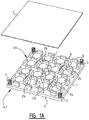
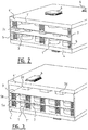
- a first embodiment of an electromechanical relay according to the invention is shown in figures 1A-1C .
- the relay comprises a carrier 4 onto which a number of coils 1 are mounted.
- the carrier 4 may be implemented in the form of a PCB 4.
- the coils 1 are positioned next to each other onto the PCB 4 and in a plane parallel to the PCB 4.
- sixteen coils 1 have been provided. It has to be understood by a person skilled in the art that this number is not meant to be limiting in any way, a relay according to embodiments of the invention can have any number of coils 1 as required for the relevant application.
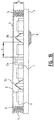
- a contact body 3 is movably mounted with respect to PCB 4 by means a number of springs 5.
- the contact body 3 may be provided in the form of a contact plate 3 made out of a magnetic material, for example an iron alloy.
- the contact body 3 may be a PCB on which or in which one or more permanent magnets are provided.
- Each of the at least one coil (1) may have an axis that is oriented perpendicular to the carrier (4) and/or the contact body (3).
- four springs 5 are provided in between PCB 4 and contact plate 3 at the corners of the PCB 4 and the contact plate 3.
- more or less than four springs 5 may be provided, and that the springs 5 can be provided at other positions than in the corners.
- springs 5 may, according to some embodiments of the invention, also have an additional function, for example the function of an electrical conduction between the contact plate 3 and a conductive path on PCB 4 which is connected to an electronic component 6 that is mounted on PCB 4.
- the ends of the springs 5 may preferably be attached directly to contact plate 3 at the one end and to PCB 4 at the other end.
- the relay furthermore comprises a number of electrical contact elements, here in the form of a pillar-shaped electrically conductive element 2a and four electrically conductive spring elements 2b. These contact elements 2a, 2b are intended to make contact with the contact plate 3 in the closed position of the relay. Providing a current through the coils 1 allows for a movement of the contact plate 3 in the direction of the carrier 4, in order to establish an electrical contact between contact plate 3 and contact elements 2a, 2b. According to embodiments of the invention that have not been illustrated, it is also possible that the relay is originally closed (i.e. that an electrical contact is present between contact plate 3 and contact elements 2a, 2b) and that charging the coils 1 causes the movement of the contact plate 3 away from the carrier 4 in such a way that the electrical contact is disconnected.
- the coils 1 are provided on a flat top surface of PCB 4, but, according to alternative embodiments, the coils 1 may also be provided in cavities in the PCB 4 or as conductive tracks of PCB 4 in the shape of so-called PCB track coils.
- the coils 1 and the contact plate 3 are provided on a top side 41 of PCB 4, and the bottom side 42 of PCB 4 is intended for mounting additional electronic components 6.
- additional electronic components 6 it is also possible to provide additional electronic components 6 at the top side 41 of PCB 4 or at the top or bottom of contact plate 3, see also the embodiment of figure 4 which is discussed below.
- the distance D (see figure 1B ) between PCB 4 and contact plate 3 may preferably be relatively small, for example less than 5 mm in the condition in which the contact elements 2a, 2b do not make contact with the contact plate 3, in such a way that a thin compact unit is obtained.
- the distance D between PCB 4 and contact plate 3 may preferably be less than 1.5 times the diameter d (1.5*d) of the coil 1, more preferably smaller than the diameter d of the coil 1, and most preferably less than 0.75 times the diameter d (0.75*d) of the coil 1.
- the coils 1 can be provided with a core of magnetic material. Further, the coils 1 can be surrounded by at least one element of magnetic material to close the magnetic circuit. In the example of figures 1A-1C , each coil 1 may be surrounded by four beam-shaped elements 8 of magnetic material. Further, instead of four beam-shaped elements 8, according to embodiments of the invention, also one tubular element 8 can be provided around a coil 1 (see also figure 4 ), and these elements 8 could also be attached to the contact plate 3 instead of to PCB 4.
- the relay illustrated in figures 1A-C is a so-called monostable relay, i.e. a relay of which the contact body 3 during charging of the coils 1 is kept in a first position (here a closed position) and springs back to a second position (here the open position) at the time that the charge is removed. It is, however, also possible to build the relay of figures 1A-C as a so-called bi-stable relay, i.e. a relay of which the coils 1 can move the contact body 3 from a first position to a second position and vice versa (for example, by reversing the direction of the current sent through the coils 1), and of which the contact body 3 after the removal of the charge stays in the relevant position.
- a so-called monostable relay i.e. a relay of which the contact body 3 during charging of the coils 1 is kept in a first position (here a closed position) and springs back to a second position (here the open position) at the time that the charge is
- one or more springs 5 can be implemented as so-called bi-stable spring elements, i.e. spring elements that after spring rebound or compression remain in the rebound or compressed position, respectively.
- An example of such a spring element 5 is a leaf spring, which shows a buckling phenomenon during the spring rebound and compression.
- a bi-stable spring element can easily be provided in the contact body 3, as is illustrated in figures 8A and 8B .
- the bi-stable spring elements 15 are formed by cutting out zones of the contact plate 3 and by creating a permanent bending deformation via a narrow bridge zone.
- the contact plate 3 may be sufficiently thin and/or elastic so that the bending deformed zone will, when a point force is applied, jump to the other side of the contact plate 3.
- Figures 8A and 8B illustrate one bi-stable spring element 15, but a person skilled in the art will understand that several such spring elements 15 can be installed.
- Figures 9A and 9B illustrate the operation of such a bi-stable spring element 15.
- Figure 9A illustrates the open position.
- the bi-stable spring element 15 will hereby make contact with an opposite stop 16, such that the contact plate 3 is pushed against the contact elements 2a.
- the contact plate 3 will remain in this position until again a magnetic field is generated that ensures that the contact plate 3 is moved up, away from the contact elements 2a.
- the bi-stable spring element 15 returns to the position of figure 9A .
- the bi-stable spring elements 15 can also be provided on the carrier 4.
- one or more permanent magnets can be provided on the carrier 4.
- the coils 1 are charged in such a way that the magnetic force that is generated can overcome the magnetic force of the permanent magnets in order to move the contact body 3 from the closed position to the open position. This may, for example, be achieved by sending a sufficiently high current in the reverse direction (in comparison with the direction needed to move the contact body 3 from the open to the closed position) through the coils 1.
- FIG. 2 illustrates a second embodiment of a relay. Similar parts have been indicated with the same reference numbers as in figure 1 .
- the relay comprises, similar to the relay illustrated in figure 1 , a contact body in the form of a contact plate 3, a carrier in the form of a PCB 4 and at least one coil 1, in the example given a plurality of coils 1, provided on the PCB 4.
- an additional movably mounted contact plate 3', an additional carrier in the form of PCB 4' and at a fixed distance from PCB 4, and a number of additional coils 1' for the generation of a magnetic field to move the additional contact plate 3' with respect to additional PCB 4' are provided.
- the additional coils 1' are provided on the additional PCB 4'.
- Contact plate 3 and additional contact plate 3' are facing each other and are located between PCB 4 and PCB 4'.
- the at least one electrical contact element is formed here as a number of contact paths 2c which are provided on the additional contact plate 3' on a side facing the contact plate 3.
- both coils 1 and additional coils 1' will contribute to the movement toward each other of contact plate 3 and additional contact plate 3'. In this way, the distance between the contact body 3 and the contact elements 2 can be increased.
- both the top side of PCB 4' and the bottom side of PCB 4 are available for mounting electronic components 6 thereon.
- the relay illustrated in figure 2 is a monostable relay. It is, however, also possible to build the variant of figure 2 as a so-called bi-stable relay.
- one or more springs 5 can be implemented as so-called bi-stable spring elements, as described for the embodiment of figure 1 and as illustrated in figures 8A, 8B, 9A and 9B .
- the coils 1 and 1' can be charged simultaneously or separately, or group by group (for example, four at a time), depending on whether it is desirable to obtain a single or a composed multiple relay.
- FIG. 3 illustrates a third embodiment of a relay. Similar parts have been indicated with the same reference numbers as in figure 1 .
- the relay comprises, similar to the relay illustrated in figure 1 , a contact body in the form of a contact plate 3, a carrier in the form of a PCB 4 and at least one coil 1, in the example given a plurality of coils 1.
- an additional PCB 4' is provided at a fixed distance from PCB 4.
- the contact plate 3 is provided in between the PCB 4 and the additional PCB 4 and at least one contact element 2d is provided on the additional PCB 4' on a side facing a side of the contact plate 3.
- a movably mounted intermediate plate 7, for example a PCB 7, is provided onto which a plurality of coils 1" are mounted for the generation of a magnetic field to move contact plate 3 with respect to the intermediate plate 7.
- both coils 1 and 1" will contribute to the movement of contact plate 3 in the direction of the electrical contact elements 2d.
- both the top side of PCB 4' and the bottom side of PCB 4 are available for mounting electronic components 6 thereon.
- the relay illustrated in figure 3 is a monostable relay. It is, however, also possible to build the variant of figure 3 as a so-called bi-stable relay.
- one or more springs 5a, 5b can be implemented as so-called bi-stable spring elements, as described for the embodiment of figure 1 .
- permanent magnets can further be mounted on the bottom side of PCB 4', see also the embodiment of figure 6 .
- the coils 1 and 1" can be charged simultaneously or separately, or group by group (for example, two or four at a time), depending on whether it is desirable to obtain a single or a composed multiple relay.
- Figure 4 illustrates a fourth embodiment of a relay according to the invention. Similar parts have been indicated with the same reference numbers as in figure 1 .
- the contact body is formed by a frame-shaped PCB 3. At the bottom side of PCB 3, a number of zones 18 of magnetic material are provided, which zones 18 extend above the coils 1 which are provided on the carrier 4.
- PCB 3 is provided with additional contact elements 13 formed of electrically conductive material, which are intended to make contact with electrical contact elements 2b, here implemented as spring contacts, on PCB 4.
- the coils 1 are provided on PCB 4 at a distance from each other, and additional electrical components 6, 6", 6"" are provided on the top side and/or bottom side of PCB 4.
- the opening in frame-shaped PCB 3 allows a high electronic component 6" to be provided on PCB 4, as this component 6" can stick out through the opening.
- electrical components 6', 6"' can for example also be provided on the bottom and the top of PCB 3.
- the monostable relay illustrated in figure 4 can also be built as a so-called bi-stable relay, as described in the embodiment of figure 1 .
- the coils 1 can be charged simultaneously or separately, or in groups, depending on whether it is desirable to obtain a single or a composed multiple relay.
- the two coils 1 on the left can, for example, be charged simultaneously in order to realize a contact between contact elements 2b, 13 on the left, and the two coils 1 on the right can be charged simultaneously in order to realize a contact between contact elements 2b, 13 on the right, wherein the coils 1 on the left and the coils 1 on the right can be charged independently from each other.
- Figure 5 illustrates a fifth embodiment of a relay according to the invention. Similar parts have been indicated with the same reference numbers as in figure 1 .
- the coils 1 are relatively high and slim compared to the rather flat coils of the embodiments illustrated in figures 1 to 4 .
- the springs 5 are here implemented as windings around the coils 1. In this way, a space is created between PCB 3 and PCB 4, where relatively high electronic components 6 can be provided.
- the contact elements are not illustrated, but may, for example, be similar to those of figures 1A-C or those of figure 4 .
- FIG. 6 illustrates a sixth embodiment of a relay according to the invention. Similar parts have been indicated with the same reference numbers as in figure 1 .
- an additional PCB 4' is provided at a fixed distance of PCB 4.
- the at least one electrical contact element is here implemented as a number of contact paths 2a, 2d, which are provided on the top side 41 of PCB 4 and at the bottom side of additional PCB 4', respectively. These contact paths 2a, 2d are intended to cooperate with corresponding contact paths 13a, 13d at respectively the bottom and top of contact body 3. Both the top of PCB 4' and the bottom of PCB 4 are available for mounting electronic components 6 thereon.
- the relay furthermore comprises springs 5.
- the springs 5 may be such that the contact paths 13d in a first position of rest make contact with contact paths 2d.
- contact plate 3 By charging coils 1, contact plate 3 can be moved to a second position in which the contact paths 13a make contact with the contact paths 2a. In this way, a two-way circuit can be realized.
- the springs 5 are such that the contact paths 13d in an intermediary position do not make contact with contact paths 2d and that the contact paths 13a do not make contact with the contact paths 2a.
- the contact plate 3 By charging the coils 1 in respectively a first direction and a second direction opposite to the first direction, the contact plate 3 can be moved to a first position in which the contact paths 13d make contact with the contact paths 2d, and to a second position in which the contact paths 13a make contact with the contact paths 2a.
- permanent magnets 9 may be provided at the bottom of additional PCB 4' and/or at the top of PCB 4 in order to keep the contact plate 3 in the first or second position in case of removal of the charge.
- FIG. 7 illustrates a seventh embodiment of a relay according to the invention. Similar parts have been indicated with the same reference numbers as in figure 1 .
- the relay according to the seventh embodiment comprises:
- the springs 5, 5' may be such that the contact paths 13b in an intermediary position do not make contact with contact paths 13b' and that the contact paths 13a, 13a' do not make contact with the contact paths 2a, 2a' (situation illustrated in figure 7 ).
- the contact plate 3 By charging the coils 1 in a first direction and a second direction opposite to the first direction, respectively, the contact plate 3 can be moved to a first position in which the contact paths 13a make contact with the contact paths 2a, and to a second position in which the contact paths 13b make contact with the contact paths 13b'.
- the contact plate 3' By charging the coils 1' in a first and a second opposite direction, respectively, the contact plate 3' can be moved to a first position in which the contact paths 13a' make contact with the contact paths 2a', and to a second position in which the contact paths 13b make contact with the contact paths 13b'. Further, the coils 1, 1' can be charged simultaneously or separately. A person skilled in the art will understand that in this way a plurality of switch combinations can be realized with a very compact relay.
- both the top of PCB 4' and the bottom of PCB 4 are available for mounting electronic components 6 thereon.
- the contact plates 3, 3' will in certain situations take a tilted position.
- the contact elements 2a, 2a', 13a, 13a', 13b, 13b' can, for example, have a rounded shape, as schematically shown in figure 7 .
- the above-described electrical contact elements 2a, 2a', 2b, 2c, 2d can, by means of conductive tracks on the PCB 4, be connected to a circuit in which the relay function should be provided.
- contact plate 3 first, second, third and fifth embodiment
- contact elements 13, 13a, 13a', 13b, 13b' fourth, sixth and seventh embodiment
- This circuit can partially or fully be provided onto a carrier/PCB 4, 4' or a contact body/PCB 3.
- the coils 1 are always mounted to or in a fixed carrier in the shape of PCB 4 or additional carrier in the shape of PCB 4'. However, it is also possible to mount the coils 1 onto or in the contact body 3 or additional contact body 3' and to install the necessary magnetic zones 18 on or in PCB 4 or PCB 4'.
- the frame-shaped contact plate of figure 4 can also be used in the embodiments of figures 1A-C , 2 , 3 , 5 , 6 , 7 , where the contact elements should of course be provided in locations that have been adapted to the electrically conductive zone(s) of the contact body/PCB 3.
Description
- The present invention relates to an electromechanical relay according to the preamble of
claim 1. More particularly, the present invention relates to an electromechanical relay that fits into electrical devices with limited space or special shapes. -
US 2003/174038 discloses arelay 7 comprising a firstnon-flexible substrate 16 and a second flexible substrate 40, seefigure 1 below. There is provided a conductive member 17 on top of thefirst substrate 16 and the conductive member 50 on top of the second flexible substrate 40. Further, there is provided a coil 22 in coil support structure 11 attached to thesecond substrate 16. Opposite the coil 22, on top of the flexible substrate 40, there is provided a ferritic member 48. The description explains that although only two coils are shown, the array may have a 10x10 array or larger to provide a multitude of independent or dependent relay circuits as desired. - A known electromechanical relay typically comprises a coil that is mounted on a base made of, for example, iron (yoke), an armature of magnetic material which is movable with respect to the base, and a first contact element made out of electrically conductive material and connected to the armature. The first contact element is intended to establish or disconnect electrical contact with a second contact element, depending on whether the coil has been charged or not. By sending a current through the coil, a magnetic field is generated for moving the armature in such a way that the electrical contact between the first contact element and the second contact element is established or disconnected. Such a relay has as a disadvantage that it is not very compact, and, therefore, difficult to integrate into small electrical devices of which the space within the device is limited and/or of which the shape is fixed.
- The aim of the present invention is to provide an electromechanical relay, the shape of which can be adapted to any desired shape of electrical device. In particular a relay is provided that, together with other electronic components, can fit into any kind of electrical device shape with a limited volume, and, more in particular, a compact relay that can form a relatively thin, flat unit.
- For this purpose, an electromechanical relay according to the invention has the features of
claim 1. The electromechanical relay comprises a carrier, a contact body which is connected to the carrier and which is movably mounted with respect to the carrier, at least one electrical contact element, and at least two coils to move the contact body with respect to the carrier, in order to disconnect or establish an electrical contact between the contact body and the at least one electrical contact element. The contact body is adapted to be moved as a result of a magnetic field generated by the at least two coils. The at least two coils are provided on or in the carrier and/or on or in the contact body. The carrier and/or the contact body are made out of electrically insulating material, on or in which electrically conductive tracks are provided. The carrier and/or the contact body are further adapted for mounting electronic components thereon, which electronic components are connectable to the electrically conductive tracks. - Embodiments of the invention are inter alia based on the inventive insight to combine a plurality of coils with a relatively small height next to each other between a carrier and a contact body, and to give an additional function to the carrier and/or contact body, namely forming a mounting surface for electronic components, like resistors, capacitors, chips, etc. In this way, a relay can be obtained with any desired shape, and, in particular, a relatively thin and compact relay can be provided that is easy to integrate in an electronic circuit.
- According to embodiments of the invention, the contact body is connected to the carrier and is, therefore, not floating.
- A plurality of coils is located next to each other in a plane parallel to the carrier and/or the contact body. The axes of the coils may preferably be substantially perpendicular to the carrier and/or the contact body. The coils can be mounted onto the carrier and/or onto the contact body, whereby, for example, also at least a first coil can be mounted onto the carrier and at least a second coil onto the contact body.
- The carrier and/or the contact body may preferably be implemented as a printed circuit board (PCB). The contact body and/or the carrier are preferably plate-shaped and may preferably be thin plates so that a thin assembly can be obtained. These plates can have any shape depending on the design of the electronic device in which the relay is required. Furthermore, the shape of the carrier can be different from or equal to the shape of the contact body. The carrier may preferably have a thickness of less than 3 mm. The contact body may preferably have a thickness of less than 3 mm.
- According to a possible embodiment, the contact body may entirely be made out of a magnetic material, for example an iron alloy. According to another embodiment, the contact body may have zones of magnetic material, which are provided in such a way that they can cooperate with the coils, to guide the magnetic flux. According to still further embodiments, for example, one or more permanent magnets may be provided onto or in the contact body.
- According to an advantageous embodiment, at least one spring means may be provided between the carrier and the contact body. The or each spring means may preferably have a first end that is fixed to the carrier and a second end that is fixed to the contact body. Using more than one coil and a spring-mounted assembly of the contact body allows the height of the relay to be limited and/or any desired height to be obtained. The contact body may, according to embodiments of the invention, also in another way resilient, hingedly or otherwise movably be hung up or mounted with respect to the carrier.
- According to embodiments of the invention, the or each spring may be adapted to form an electrically conductive path between the carrier and the contact body.
- According to a possible embodiment, the carrier may have a first side on which the at least two coils and the contact body are provided and a second side, opposite to the first side, on which an invention, also in another way resilient, hingedly or otherwise movably be hung up or mounted with respect to the carrier.
- According to embodiments of the invention, the or each spring may be adapted to form an electrically conductive path between the carrier and the contact body.
- According to a possible embodiment, the carrier may have a first side on which the at least two coils and the contact body are provided and a second side, opposite to the first side, on which an electronic component is provided. Further, one or more electronic components can also be provided on this first side. Furthermore, one or more electronic components can be provided on one side of the contact body or on both sides thereof.
- The at least one contact element is provided directly to the carrier on a side facing the contact body. In other embodiments, not claimed in this application, it can also be provided at a different location, for example at a distance from the carrier, on the other side of the contact body. The at least one contact element is provided between two adjacent coils on the carrier.
- According to advantageous embodiments of the invention, at least four coils may be provided, which are placed next to each other in a plane between the carrier and the contact body. This will allow the distance between the carrier and the contact body to be kept relatively small, while the coils can exert a sufficiently large force on the contact body without very high currents being required. The distance between the carrier and the contact body, in the condition in which the at least one contact element does not make contact with the contact body, may preferably be less than 1.5 times the diameter (1.5*d) of a coil, more preferably smaller than the diameter of the coil, and most preferably less than 0.75 times the diameter (0.75*d) of the coil. This distance may preferably be less than 10 mm, or more preferably less than 5 mm.
- The at least one electrical contact element may, for example, comprise a spring contact or a spherical contact. More generally, the at least one electrical contact element can have any shape. Furthermore, contact elements of different types can be combined in one relay.
- According to an advantageous embodiment, the carrier and/or the contact body may be a PCB, and each coil may be formed with conductive tracks of the PCB (PCB track coil). Hereby the conductive tracks may, according to embodiments of the invention, be provided in multiple layers of the PCB. In this way, the compactness of the relay can be further enhanced.
- According to an embodiment invention, each coil may be provided with a core of magnetic material. Further, each coil can also be surrounded by at least one element of magnetic material in order to, together with the at least one coil and the contact body, form a magnetic circuit. Such an element can be mounted against the contact body or against the carrier. Furthermore, such an element can be resilient or spring-mounted. When the contact body, as a result of charging the at least one coil, moves in the direction of the carrier, such a spring element of magnetic material can then be pushed in.
- The relay may comprise an additional movably mounted contact body, an additional carrier, and at least two additional coils to generate a magnetic field for moving the additional contact body with respect to the additional carrier. The contact body and the additional contact body are hereby facing each other and are located between the carrier and the additional carrier. The additional carrier may be located at a fixed distance from the carrier, and the at least one contact element may be provided on or may be formed by the additional contact body. In this way, the relay function is thus built in between two carriers, wherein two sets of coils located above each other are present between the carriers, and wherein additional electronic components can be mounted onto the carriers. The carriers may preferably be PCBs.
- The relay may comprise an additional carrier at a fixed distance from the carrier. The additional carrier is provided with at least one contact element at a side facing a side of the contact body. Between the contact body and the carrier, there may be a movable intermediate body, typically a separator plate, on which or in which at least two additional coils are provided for the generation of a magnetic field to move the contact body with respect to the intermediate body. In this way, the distance between the contact body and the at least one contact element (in the open position) can be increased. Also two sets of coils, which contribute to the movement of the contact body with respect to the carrier, are provided above each other. Furthermore, other electronic components can be provided on both the carrier and the additional carrier.
- According to a possible embodiment, the at least one contact element may comprise at least a first contact element on a first side of the contact body and at least a second contact element on a second side of the contact body, and the contact body may be mounted and designed so as to make electrical contact with the first contact element in a first position and with the second contact element in a second position. In this way, a two-way circuit can be formed, in which the contact body alternately makes contact with the first contact element and the second contact element.
- According to a possible embodiment, the contact body may be movable between a first and a second position as a result of the generation of respectively a first and a second magnetic field by means of the at least two coils. This is called a bi-stable relay. To obtain a bi-stable relay, at least one permanent magnet may be provided onto the carrier and/or the contact body in such a way that the contact body is kept in the first position after removal of the first magnetic field and/or that the contact body is kept in the second position after removal of the second magnetic field. According to embodiments of the invention, the contact body may be spring-mounted with respect to the carrier by means of at least one bi-stable spring element, whereby the at least one bi-stable spring element is mounted in such a way that the contact body is kept in the first position after removal of the first magnetic field and/or that the contact body is kept in the second position after removal of the second magnetic field.
- According to a further developed embodiment, the at least one contact element may comprise a first contact element and a second contact element, and the at least two coils are provided in such a way that, as a result of selectively charging one or more of these coils, the first and second contact element can selectively make contact with the contact body. In this way, compact multiple relays can be built.
- The present invention will be further explained on the basis of a number of, by no means limiting, exemplary embodiments of an electromechanical relay according to the invention, with reference to the attached drawings.
-
Figure 1A schematically illustrates an exploded perspective view of a first embodiment of a relay according to the invention; -
Figure 1B schematically illustrates a side view of the embodiment offigure 1A ; -
Figure 1C schematically illustrates a top view of the embodiment offigure 1A ; -
Figure 2 schematically illustrates a perspective view of a second embodiment of a relay; -
Figure 3 schematically illustrates a perspective view of a third embodiment of a relay; -
Figure 4 schematically illustrates an exploded perspective view of a fourth embodiment of a relay according to the invention; -
Figure 5 schematically illustrates a perspective view of a fifth embodiment of a relay according to the invention; -
Figure 6 schematically illustrates a perspective view of a sixth embodiment of a relay according to the invention; -
Figure 7 schematically illustrates a perspective view of a seventh embodiment of a relay according to the invention; -
Figures 8A and 8B schematically illustrate a view of a bi-stable spring element in two different positions; and -
Figures 9A and 9B schematically illustrate a view of an embodiment of a relay according to the invention in two different positions. - A first embodiment of an electromechanical relay according to the invention is shown in
figures 1A-1C . The relay comprises acarrier 4 onto which a number ofcoils 1 are mounted. According the present embodiment, thecarrier 4 may be implemented in the form of aPCB 4. Thecoils 1 are positioned next to each other onto thePCB 4 and in a plane parallel to thePCB 4. In the illustrated example, sixteencoils 1 have been provided. It has to be understood by a person skilled in the art that this number is not meant to be limiting in any way, a relay according to embodiments of the invention can have any number ofcoils 1 as required for the relevant application. Acontact body 3 is movably mounted with respect toPCB 4 by means a number ofsprings 5. According to the present embodiment, thecontact body 3 may be provided in the form of acontact plate 3 made out of a magnetic material, for example an iron alloy. According to further embodiments of the invention which have not been illustrated, thecontact body 3 may be a PCB on which or in which one or more permanent magnets are provided. Each of the at least one coil (1) may have an axis that is oriented perpendicular to the carrier (4) and/or the contact body (3). In the illustrated example, foursprings 5 are provided in betweenPCB 4 andcontact plate 3 at the corners of thePCB 4 and thecontact plate 3. A person skilled in the art will understand that, according to embodiments of the invention, more or less than foursprings 5 may be provided, and that thesprings 5 can be provided at other positions than in the corners. Thesesprings 5 may, according to some embodiments of the invention, also have an additional function, for example the function of an electrical conduction between thecontact plate 3 and a conductive path onPCB 4 which is connected to anelectronic component 6 that is mounted onPCB 4. In order to keep the distance betweencontact plate 3 andPCB 4 small, the ends of thesprings 5 may preferably be attached directly to contactplate 3 at the one end and toPCB 4 at the other end. - The relay furthermore comprises a number of electrical contact elements, here in the form of a pillar-shaped electrically
conductive element 2a and four electricallyconductive spring elements 2b. Thesecontact elements contact plate 3 in the closed position of the relay. Providing a current through thecoils 1 allows for a movement of thecontact plate 3 in the direction of thecarrier 4, in order to establish an electrical contact betweencontact plate 3 andcontact elements contact plate 3 andcontact elements coils 1 causes the movement of thecontact plate 3 away from thecarrier 4 in such a way that the electrical contact is disconnected. - In the present embodiment, the
coils 1 are provided on a flat top surface ofPCB 4, but, according to alternative embodiments, thecoils 1 may also be provided in cavities in thePCB 4 or as conductive tracks ofPCB 4 in the shape of so-called PCB track coils. - In the embodiment illustrated in
figures 1A-1C , thecoils 1 and thecontact plate 3 are provided on atop side 41 ofPCB 4, and thebottom side 42 ofPCB 4 is intended for mounting additionalelectronic components 6. However, it is also possible to provide additionalelectronic components 6 at thetop side 41 ofPCB 4 or at the top or bottom ofcontact plate 3, see also the embodiment offigure 4 which is discussed below. - The distance D (see
figure 1B ) betweenPCB 4 andcontact plate 3 may preferably be relatively small, for example less than 5 mm in the condition in which thecontact elements contact plate 3, in such a way that a thin compact unit is obtained. The distance D betweenPCB 4 andcontact plate 3 may preferably be less than 1.5 times the diameter d (1.5*d) of thecoil 1, more preferably smaller than the diameter d of thecoil 1, and most preferably less than 0.75 times the diameter d (0.75*d) of thecoil 1. - According to embodiments of the invention, the
coils 1 can be provided with a core of magnetic material. Further, thecoils 1 can be surrounded by at least one element of magnetic material to close the magnetic circuit. In the example offigures 1A-1C , eachcoil 1 may be surrounded by four beam-shapedelements 8 of magnetic material. Further, instead of four beam-shapedelements 8, according to embodiments of the invention, also onetubular element 8 can be provided around a coil 1 (see alsofigure 4 ), and theseelements 8 could also be attached to thecontact plate 3 instead of toPCB 4. - The relay illustrated in
figures 1A-C is a so-called monostable relay, i.e. a relay of which thecontact body 3 during charging of thecoils 1 is kept in a first position (here a closed position) and springs back to a second position (here the open position) at the time that the charge is removed. It is, however, also possible to build the relay offigures 1A-C as a so-called bi-stable relay, i.e. a relay of which thecoils 1 can move thecontact body 3 from a first position to a second position and vice versa (for example, by reversing the direction of the current sent through the coils 1), and of which thecontact body 3 after the removal of the charge stays in the relevant position. For this purpose, one ormore springs 5 can be implemented as so-called bi-stable spring elements, i.e. spring elements that after spring rebound or compression remain in the rebound or compressed position, respectively. An example of such aspring element 5 is a leaf spring, which shows a buckling phenomenon during the spring rebound and compression. According to embodiments of the present invention, such a bi-stable spring element can easily be provided in thecontact body 3, as is illustrated infigures 8A and 8B . Thebi-stable spring elements 15 are formed by cutting out zones of thecontact plate 3 and by creating a permanent bending deformation via a narrow bridge zone. According to typical embodiments, thecontact plate 3 may be sufficiently thin and/or elastic so that the bending deformed zone will, when a point force is applied, jump to the other side of thecontact plate 3.Figures 8A and 8B illustrate onebi-stable spring element 15, but a person skilled in the art will understand that severalsuch spring elements 15 can be installed.Figures 9A and 9B illustrate the operation of such abi-stable spring element 15.Figure 9A illustrates the open position. When thecontact plate 3 is attracted as a result of a magnetic field generated by thecoil 1, thebi-stable spring element 15 is pressed against thecarrier 4, and it will jump to its reversed fixed position, seefigure 9B . Thebi-stable spring element 15 will hereby make contact with anopposite stop 16, such that thecontact plate 3 is pushed against thecontact elements 2a. Thecontact plate 3 will remain in this position until again a magnetic field is generated that ensures that thecontact plate 3 is moved up, away from thecontact elements 2a. At that time, thebi-stable spring element 15 returns to the position offigure 9A . According to a further embodiment that is not illustrated, thebi-stable spring elements 15 can also be provided on thecarrier 4. - According to embodiments of the invention, one or more permanent magnets (not shown in
figures 1A-C ) can be provided on thecarrier 4. To allow movement of thecontact body 3 from the closed position to the open position, thecoils 1 are charged in such a way that the magnetic force that is generated can overcome the magnetic force of the permanent magnets in order to move thecontact body 3 from the closed position to the open position. This may, for example, be achieved by sending a sufficiently high current in the reverse direction (in comparison with the direction needed to move thecontact body 3 from the open to the closed position) through thecoils 1. - Although in the description above, it was described to charge the
coils 1 simultaneously so as to move thecontact body 3 from a closed position to an open position and vice versa, a person skilled in the art will understand that it is also possible to charge the coils not simultaneously, so that thecontact body 3 is, for example, tilted, and not all contacts are closed. Thecontact elements coils 1 will then allow the selective contact of thecontact elements contact body 3 so that multiple independent switching electrical circuits can be realized. This will make multi-switch actions possible, and it will, for example, be possible to obtain an electrical two-way circuit. -
Figure 2 illustrates a second embodiment of a relay. Similar parts have been indicated with the same reference numbers as infigure 1 . The relay comprises, similar to the relay illustrated infigure 1 , a contact body in the form of acontact plate 3, a carrier in the form of aPCB 4 and at least onecoil 1, in the example given a plurality ofcoils 1, provided on thePCB 4. According to the second embodiment, an additional movably mounted contact plate 3', an additional carrier in the form of PCB 4' and at a fixed distance fromPCB 4, and a number of additional coils 1' for the generation of a magnetic field to move the additional contact plate 3' with respect to additional PCB 4', are provided. The additional coils 1' are provided on the additional PCB 4'.Contact plate 3 and additional contact plate 3' are facing each other and are located betweenPCB 4 and PCB 4'. The at least one electrical contact element is formed here as a number of contact paths 2c which are provided on the additional contact plate 3' on a side facing thecontact plate 3. According to the present embodiment, bothcoils 1 and additional coils 1' will contribute to the movement toward each other ofcontact plate 3 and additional contact plate 3'. In this way, the distance between thecontact body 3 and the contact elements 2 can be increased. Furthermore, both the top side of PCB 4' and the bottom side ofPCB 4 are available for mountingelectronic components 6 thereon. - The relay illustrated in
figure 2 is a monostable relay. It is, however, also possible to build the variant offigure 2 as a so-called bi-stable relay. For this purpose, one ormore springs 5 can be implemented as so-called bi-stable spring elements, as described for the embodiment offigure 1 and as illustrated infigures 8A, 8B, 9A and 9B . - Also for the variant of
figure 2 , thecoils 1 and 1' can be charged simultaneously or separately, or group by group (for example, four at a time), depending on whether it is desirable to obtain a single or a composed multiple relay. -
Figure 3 illustrates a third embodiment of a relay. Similar parts have been indicated with the same reference numbers as infigure 1 . The relay comprises, similar to the relay illustrated infigure 1 , a contact body in the form of acontact plate 3, a carrier in the form of aPCB 4 and at least onecoil 1, in the example given a plurality ofcoils 1. According to the third embodiment, an additional PCB 4' is provided at a fixed distance fromPCB 4. Thecontact plate 3 is provided in between thePCB 4 and theadditional PCB 4 and at least onecontact element 2d is provided on the additional PCB 4' on a side facing a side of thecontact plate 3. Between thecontact plate 3 andPCB 4, a movably mountedintermediate plate 7, for example aPCB 7, is provided onto which a plurality ofcoils 1" are mounted for the generation of a magnetic field to movecontact plate 3 with respect to theintermediate plate 7. In this way, bothcoils contact plate 3 in the direction of theelectrical contact elements 2d. Furthermore, both the top side of PCB 4' and the bottom side ofPCB 4 are available for mountingelectronic components 6 thereon. - The relay illustrated in
figure 3 is a monostable relay. It is, however, also possible to build the variant offigure 3 as a so-called bi-stable relay. For this purpose, one ormore springs figure 1 . According to embodiments of the invention, permanent magnets can further be mounted on the bottom side of PCB 4', see also the embodiment offigure 6 . - Also for the variant of
figure 3 , thecoils -
Figure 4 illustrates a fourth embodiment of a relay according to the invention. Similar parts have been indicated with the same reference numbers as infigure 1 . According to the fourth embodiment, the contact body is formed by a frame-shapedPCB 3. At the bottom side ofPCB 3, a number ofzones 18 of magnetic material are provided, whichzones 18 extend above thecoils 1 which are provided on thecarrier 4. Furthermore,PCB 3 is provided withadditional contact elements 13 formed of electrically conductive material, which are intended to make contact withelectrical contact elements 2b, here implemented as spring contacts, onPCB 4. According to the fourth embodiment, thecoils 1 are provided onPCB 4 at a distance from each other, and additionalelectrical components PCB 4. Furthermore, the opening in frame-shapedPCB 3 allows a highelectronic component 6" to be provided onPCB 4, as thiscomponent 6" can stick out through the opening. Furthermore,electrical components 6', 6"' can for example also be provided on the bottom and the top ofPCB 3. - The monostable relay illustrated in
figure 4 can also be built as a so-called bi-stable relay, as described in the embodiment offigure 1 . - Also for the variant of
figure 4 , thecoils 1 can be charged simultaneously or separately, or in groups, depending on whether it is desirable to obtain a single or a composed multiple relay. The twocoils 1 on the left can, for example, be charged simultaneously in order to realize a contact betweencontact elements coils 1 on the right can be charged simultaneously in order to realize a contact betweencontact elements coils 1 on the left and thecoils 1 on the right can be charged independently from each other. -
Figure 5 illustrates a fifth embodiment of a relay according to the invention. Similar parts have been indicated with the same reference numbers as infigure 1 . According to the fifth embodiment, thecoils 1 are relatively high and slim compared to the rather flat coils of the embodiments illustrated infigures 1 to 4 . Thesprings 5 are here implemented as windings around thecoils 1. In this way, a space is created betweenPCB 3 andPCB 4, where relatively highelectronic components 6 can be provided. The contact elements are not illustrated, but may, for example, be similar to those offigures 1A-C or those offigure 4 . -
Figure 6 illustrates a sixth embodiment of a relay according to the invention. Similar parts have been indicated with the same reference numbers as infigure 1 . According to the sixth embodiment, an additional PCB 4' is provided at a fixed distance ofPCB 4. The at least one electrical contact element is here implemented as a number ofcontact paths top side 41 ofPCB 4 and at the bottom side of additional PCB 4', respectively. Thesecontact paths corresponding contact paths contact body 3. Both the top of PCB 4' and the bottom ofPCB 4 are available for mountingelectronic components 6 thereon. - The relay furthermore comprises springs 5. According to a first possibility, the
springs 5 may be such that thecontact paths 13d in a first position of rest make contact withcontact paths 2d. By chargingcoils 1,contact plate 3 can be moved to a second position in which thecontact paths 13a make contact with thecontact paths 2a. In this way, a two-way circuit can be realized. - According to a second possibility, which is illustrated in
figure 6 , thesprings 5 are such that thecontact paths 13d in an intermediary position do not make contact withcontact paths 2d and that thecontact paths 13a do not make contact with thecontact paths 2a. By charging thecoils 1 in respectively a first direction and a second direction opposite to the first direction, thecontact plate 3 can be moved to a first position in which thecontact paths 13d make contact with thecontact paths 2d, and to a second position in which thecontact paths 13a make contact with thecontact paths 2a. Further,permanent magnets 9 may be provided at the bottom of additional PCB 4' and/or at the top ofPCB 4 in order to keep thecontact plate 3 in the first or second position in case of removal of the charge. -
Figure 7 illustrates a seventh embodiment of a relay according to the invention. Similar parts have been indicated with the same reference numbers as infigure 1 . The relay according to the seventh embodiment comprises: - an additional PCB 4' at a fixed distance from
PCB 4; - an additional contact plate 3' spring-mounted with respect to PCB 4' by means of springs 5', at the bottom thereof; and
- additional coils 1' for moving contact plate 3' with respect to PCB 4'.
- The
springs 5, 5' may be such that thecontact paths 13b in an intermediary position do not make contact withcontact paths 13b' and that thecontact paths contact paths figure 7 ). By charging thecoils 1 in a first direction and a second direction opposite to the first direction, respectively, thecontact plate 3 can be moved to a first position in which thecontact paths 13a make contact with thecontact paths 2a, and to a second position in which thecontact paths 13b make contact with thecontact paths 13b'. By charging the coils 1' in a first and a second opposite direction, respectively, the contact plate 3' can be moved to a first position in which thecontact paths 13a' make contact with thecontact paths 2a', and to a second position in which thecontact paths 13b make contact with thecontact paths 13b'. Further, thecoils 1, 1' can be charged simultaneously or separately. A person skilled in the art will understand that in this way a plurality of switch combinations can be realized with a very compact relay. - Similar as in the embodiment described with respect to, for example,
figures 3 and4 , both the top of PCB 4' and the bottom ofPCB 4 are available for mountingelectronic components 6 thereon. - If in the embodiment illustrated in
figure 7 thecoils 1, 1' are charged alternately in order to selectively close or open certain contacts, thecontact plates 3, 3' will in certain situations take a tilted position. In order to realize a proper contact in such a position as well, thecontact elements figure 7 . - The above-described
electrical contact elements PCB 4, be connected to a circuit in which the relay function should be provided. Similarly, contact plate 3 (first, second, third and fifth embodiment) orcontact elements PCB 4, 4' or a contact body/PCB 3. - In the illustrated embodiments, the
coils 1 are always mounted to or in a fixed carrier in the shape ofPCB 4 or additional carrier in the shape of PCB 4'. However, it is also possible to mount thecoils 1 onto or in thecontact body 3 or additional contact body 3' and to install the necessarymagnetic zones 18 on or inPCB 4 or PCB 4'. - A person skilled in the art will understand that different embodiments can be combined with each other. For example, the frame-shaped contact plate of
figure 4 can also be used in the embodiments offigures 1A-C ,2 ,3 ,5 ,6 ,7 , where the contact elements should of course be provided in locations that have been adapted to the electrically conductive zone(s) of the contact body/PCB 3. - A person skilled in the art will understand that many modifications and additions are possible within the framework of the present invention, which in no way is limited by the exemplary embodiments described above. The scope of protection is only determined by the following claims.
Claims (14)
- Electromechanical relay comprising:- a carrier (4);- a contact body (3), movably mounted with respect to the carrier (4);- at least one electrical contact element (2a;2b;2c;2d);- at least two coils (1) for moving the contact body (3) with respect to the carrier (4), so as to disconnect or establish an electrical contact between the contact body (3) and the at least one electrical contact element (2a;2b;2c;2d),wherein the contact body (3) is adapted to move as a result of a magnetic field generated by the at least two coils (1), wherein the at least two coils (1) are mounted on or in the carrier (4) and/or on or in the contact body (3), and wherein the carrier (4) and/or the contact body (3)- are made out of an electrically insulating material, on which or in which electrically conductive tracks are provided, and- are adapted for providing electronic components (6) thereon, which electronic components (6) are connectable to the electrically conductive tracks; wherein the at least two coils (1) are placed next to each other, seen in a plane parallel to the carrier (4) and/or the contact body (3);wherein the at least one contact element (2a;2b;2c;2d) is provided directly to the carrier (4) on a side of the carrier facing the contact body (3), characterized in that the at least one electrical contact element (2a;2b;2c;2d) is provided between adjacent coils on the carrier of the at least two coils (1).
- Electromechanical relay according to claim 1, wherein the carrier (4) and/or the contact body (3) is a printed circuit board (PCB).
- Electromechanical single relay according to claim 1 or 2, wherein the at least one electrical contact comprises a spring contact or a spherical contact.
- Electromechanical relay according to any of the previous claims, wherein the or each coil (1) has an axis that is oriented perpendicular to the carrier (4) and/or the contact body (3).
- Electromechanical relay according to any of the previous claims, wherein the contact body (3)- has been fully made out of a magnetic material; or- comprises zones (18) of magnetic material; and/or- is provided with one or more permanent magnets (9).
- Electromechanical relay according to any of the previous claims, wherein at least one spring means (5;5a,5b) is provided between the carrier (4) and the contact body (3).
- Electromechanical relay according to claim 6, wherein the or each spring means (5;5a,5b) has a first end that is attached to the carrier (4) and a second end that is attached to the contact body (3).
- Electromechanical relay according to claim 6 or 7, wherein the or each spring means (5;5a,5b) is adapted to form an electrically conductive path between the carrier (4) and the contact body (3).
- Electromechanical relay according to any of the previous claims, the carrier (4) having a first side (41) and a second side (42) and the contact body (3) having a first side and a second side, wherein an electronic component (6,6",6"") is mounted on the first side (41) and/or on the second side (42) of the carrier (4); and/or
wherein an electronic component (6',6"') is mounted on the first and/or on the second side of the contact body (3). - Electromechanical relay according to any of the previous claims, wherein the distance (D) between the carrier (4) and the contact body (3), in the condition in which the at least one contact element (2a;2b;2c;2d) does not make contact with the contact body (3), is less than 5 mm.
- Electromechanical relay according to any one of the previous claims, wherein the distance between the carrier and the contact body, in the condition in which the at least one contact element does not make contact with the contact body, is smaller than the diameter of the coil.
- Electromechanical relay according to any of the previous claims, wherein the at least one contact element comprises at least a first contact element (2a) on a first side of the contact body (3) and a second contact element (2d; 13b') on a second side of the contact body (3), and the contact body (3,13a, 13d; 3, 13a, 13b) is mounted and adapted to make electrical contact with the first contact element (2a) in a first position and with the second contact element (2d; 13b') in a second position.
- Electromechanical relay according to any of the previous claims, wherein the contact body (3) is movable between a first and a second position as a result of the generation of respectively a first and a second magnetic field by the at least two coils (1), and at least one permanent magnet (9) is provided on the carrier (4) and/or the contact body (3) in such a way that the contact body (3) is kept in the first position after removal of the first magnetic field and/or that the contact body (3) is kept in the second position after removal of the second magnetic field.
- Electromechanical relay according to any of the previous claims, wherein the at least one contact element comprises a first contact element and a second contact element, and the at least two coils (1) are provided in such a way that, as a result of selectively charging one or more coils (1), the first and second contact element can selectively make contact with the contact body (3).
Priority Applications (1)
| Application Number | Priority Date | Filing Date | Title |
|---|---|---|---|
| PL14186542T PL2854150T3 (en) | 2013-09-26 | 2014-09-26 | Electromechanical relay |
Applications Claiming Priority (1)
| Application Number | Priority Date | Filing Date | Title |
|---|---|---|---|
| BE2013/0642A BE1021758B1 (en) | 2013-09-26 | 2013-09-26 | ELECTROMECHANICAL RELAY |
Publications (2)
| Publication Number | Publication Date |
|---|---|
| EP2854150A1 EP2854150A1 (en) | 2015-04-01 |
| EP2854150B1 true EP2854150B1 (en) | 2017-06-14 |
Family
ID=49596013
Family Applications (1)
| Application Number | Title | Priority Date | Filing Date |
|---|---|---|---|
| EP14186542.8A Active EP2854150B1 (en) | 2013-09-26 | 2014-09-26 | Electromechanical relay |
Country Status (5)
| Country | Link |
|---|---|
| EP (1) | EP2854150B1 (en) |
| BE (1) | BE1021758B1 (en) |
| DK (1) | DK2854150T3 (en) |
| HU (1) | HUE033350T2 (en) |
| PL (1) | PL2854150T3 (en) |
Family Cites Families (7)
| Publication number | Priority date | Publication date | Assignee | Title |
|---|---|---|---|---|
| JP3493446B2 (en) * | 1996-07-31 | 2004-02-03 | オムロン株式会社 | Matrix switch |
| DE19823987A1 (en) * | 1998-05-29 | 1999-12-02 | Thomas Frank | Electrodynamic microrelay with a permanent magnetic actuator |
| US6229417B1 (en) * | 1999-02-23 | 2001-05-08 | Rockwell Technologies, Llc | Operator for an electromagnetic switching device |
| AU784864B2 (en) * | 2001-03-15 | 2006-07-13 | Micro Relay Holdings Pty Ltd | Telecommunication relay array for DSL network configuration |
| US6734776B2 (en) * | 2002-03-13 | 2004-05-11 | Ford Global Technologies, Llc | Flex circuit relay |
| JP2007087828A (en) * | 2005-09-22 | 2007-04-05 | Matsushita Electric Works Ltd | Hybrid relay |
| US8093970B2 (en) * | 2007-10-12 | 2012-01-10 | Montara Technologies LLC | Braided electrical contact element based relay |
-
2013
- 2013-09-26 BE BE2013/0642A patent/BE1021758B1/en not_active IP Right Cessation
-
2014
- 2014-09-26 DK DK14186542.8T patent/DK2854150T3/en active
- 2014-09-26 HU HUE14186542A patent/HUE033350T2/en unknown
- 2014-09-26 EP EP14186542.8A patent/EP2854150B1/en active Active
- 2014-09-26 PL PL14186542T patent/PL2854150T3/en unknown
Also Published As
| Publication number | Publication date |
|---|---|
| BE1021758B1 (en) | 2016-01-15 |
| DK2854150T3 (en) | 2017-07-24 |
| EP2854150A1 (en) | 2015-04-01 |
| HUE033350T2 (en) | 2017-11-28 |
| PL2854150T3 (en) | 2017-10-31 |
Similar Documents
| Publication | Publication Date | Title |
|---|---|---|
| CN102024625B (en) | Electromagnetic relay | |
| CN102891039A (en) | Relay | |
| US20180241293A1 (en) | Vibration motor | |
| CA2508541C (en) | Electromagnetic relay | |
| CN102891040A (en) | Relay | |
| EP2395519B1 (en) | Bistable permanent magnetic actuator | |
| KR101023581B1 (en) | Microsystem with electromagnetic control | |
| JP4620153B2 (en) | Electrical switching device with magnetic adjustment element for switching element | |
| WO2012058323A1 (en) | Multi integrated switching device structures | |
| JP2014165152A (en) | Electromagnetic relay | |
| EP2854150B1 (en) | Electromechanical relay | |
| EP2911175B1 (en) | Electromagnetic relay | |
| CN102959672A (en) | Contact mechanism and electromagnetic contactor using same | |
| CN107408477A (en) | Relay | |
| CA2182931C (en) | Switching field | |
| EP2862193B1 (en) | Improved relay | |
| NL9101630A (en) | BISTABLE ELECTRICAL RELAY. | |
| JP6922534B2 (en) | Electromagnetic relay | |
| EP2691970B1 (en) | Modular electrical switch | |
| JP6897408B2 (en) | Electromagnetic relay | |
| KR200489019Y1 (en) | Electro-magnetic Contactor | |
| EP3211653B1 (en) | Electromagnetic relay for three switching positions | |
| EP2854151A1 (en) | Electromechanical relay | |
| KR200422243Y1 (en) | Relay having vertical module structure and relay array having the same | |
| KR102197518B1 (en) | Electromagnetic contactor |
Legal Events
| Date | Code | Title | Description |
|---|---|---|---|
| PUAI | Public reference made under article 153(3) epc to a published international application that has entered the european phase |
Free format text: ORIGINAL CODE: 0009012 |
|
| 17P | Request for examination filed |
Effective date: 20140926 |
|
| AK | Designated contracting states |
Kind code of ref document: A1 Designated state(s): AL AT BE BG CH CY CZ DE DK EE ES FI FR GB GR HR HU IE IS IT LI LT LU LV MC MK MT NL NO PL PT RO RS SE SI SK SM TR |
|
| AX | Request for extension of the european patent |
Extension state: BA ME |
|
| R17P | Request for examination filed (corrected) |
Effective date: 20150911 |
|
| RBV | Designated contracting states (corrected) |
Designated state(s): AL AT BE BG CH CY CZ DE DK EE ES FI FR GB GR HR HU IE IS IT LI LT LU LV MC MK MT NL NO PL PT RO RS SE SI SK SM TR |
|
| 17Q | First examination report despatched |
Effective date: 20160519 |
|
| GRAP | Despatch of communication of intention to grant a patent |
Free format text: ORIGINAL CODE: EPIDOSNIGR1 |
|
| INTG | Intention to grant announced |
Effective date: 20170104 |
|
| GRAS | Grant fee paid |
Free format text: ORIGINAL CODE: EPIDOSNIGR3 |
|
| GRAA | (expected) grant |
Free format text: ORIGINAL CODE: 0009210 |
|
| AK | Designated contracting states |
Kind code of ref document: B1 Designated state(s): AL AT BE BG CH CY CZ DE DK EE ES FI FR GB GR HR HU IE IS IT LI LT LU LV MC MK MT NL NO PL PT RO RS SE SI SK SM TR |
|
| REG | Reference to a national code |
Ref country code: GB Ref legal event code: FG4D |
|
| REG | Reference to a national code |
Ref country code: CH Ref legal event code: EP Ref country code: AT Ref legal event code: REF Ref document number: 901701 Country of ref document: AT Kind code of ref document: T Effective date: 20170615 |
|
| REG | Reference to a national code |
Ref country code: IE Ref legal event code: FG4D |
|
| REG | Reference to a national code |
Ref country code: NL Ref legal event code: FP |
|
| REG | Reference to a national code |
Ref country code: DK Ref legal event code: T3 Effective date: 20170720 |
|
| REG | Reference to a national code |
Ref country code: SE Ref legal event code: TRGR |
|
| REG | Reference to a national code |
Ref country code: DE Ref legal event code: R096 Ref document number: 602014010700 Country of ref document: DE |
|
| REG | Reference to a national code |
Ref country code: NO Ref legal event code: T2 Effective date: 20170614 |
|
| REG | Reference to a national code |
Ref country code: FR Ref legal event code: PLFP Year of fee payment: 4 |
|
| REG | Reference to a national code |
Ref country code: LT Ref legal event code: MG4D |
|
| PG25 | Lapsed in a contracting state [announced via postgrant information from national office to epo] |
Ref country code: LT Free format text: LAPSE BECAUSE OF FAILURE TO SUBMIT A TRANSLATION OF THE DESCRIPTION OR TO PAY THE FEE WITHIN THE PRESCRIBED TIME-LIMIT Effective date: 20170614 Ref country code: GR Free format text: LAPSE BECAUSE OF FAILURE TO SUBMIT A TRANSLATION OF THE DESCRIPTION OR TO PAY THE FEE WITHIN THE PRESCRIBED TIME-LIMIT Effective date: 20170915 Ref country code: FI Free format text: LAPSE BECAUSE OF FAILURE TO SUBMIT A TRANSLATION OF THE DESCRIPTION OR TO PAY THE FEE WITHIN THE PRESCRIBED TIME-LIMIT Effective date: 20170614 Ref country code: HR Free format text: LAPSE BECAUSE OF FAILURE TO SUBMIT A TRANSLATION OF THE DESCRIPTION OR TO PAY THE FEE WITHIN THE PRESCRIBED TIME-LIMIT Effective date: 20170614 |
|
| REG | Reference to a national code |
Ref country code: AT Ref legal event code: MK05 Ref document number: 901701 Country of ref document: AT Kind code of ref document: T Effective date: 20170614 |
|
| REG | Reference to a national code |
Ref country code: HU Ref legal event code: AG4A Ref document number: E033350 Country of ref document: HU |
|
| PG25 | Lapsed in a contracting state [announced via postgrant information from national office to epo] |
Ref country code: BG Free format text: LAPSE BECAUSE OF FAILURE TO SUBMIT A TRANSLATION OF THE DESCRIPTION OR TO PAY THE FEE WITHIN THE PRESCRIBED TIME-LIMIT Effective date: 20170914 Ref country code: RS Free format text: LAPSE BECAUSE OF FAILURE TO SUBMIT A TRANSLATION OF THE DESCRIPTION OR TO PAY THE FEE WITHIN THE PRESCRIBED TIME-LIMIT Effective date: 20170614 Ref country code: LV Free format text: LAPSE BECAUSE OF FAILURE TO SUBMIT A TRANSLATION OF THE DESCRIPTION OR TO PAY THE FEE WITHIN THE PRESCRIBED TIME-LIMIT Effective date: 20170614 |
|
| REG | Reference to a national code |
Ref country code: SK Ref legal event code: T3 Ref document number: E 24670 Country of ref document: SK |
|
| PG25 | Lapsed in a contracting state [announced via postgrant information from national office to epo] |
Ref country code: EE Free format text: LAPSE BECAUSE OF FAILURE TO SUBMIT A TRANSLATION OF THE DESCRIPTION OR TO PAY THE FEE WITHIN THE PRESCRIBED TIME-LIMIT Effective date: 20170614 Ref country code: AT Free format text: LAPSE BECAUSE OF FAILURE TO SUBMIT A TRANSLATION OF THE DESCRIPTION OR TO PAY THE FEE WITHIN THE PRESCRIBED TIME-LIMIT Effective date: 20170614 Ref country code: RO Free format text: LAPSE BECAUSE OF FAILURE TO SUBMIT A TRANSLATION OF THE DESCRIPTION OR TO PAY THE FEE WITHIN THE PRESCRIBED TIME-LIMIT Effective date: 20170614 |
|
| PG25 | Lapsed in a contracting state [announced via postgrant information from national office to epo] |
Ref country code: IT Free format text: LAPSE BECAUSE OF FAILURE TO SUBMIT A TRANSLATION OF THE DESCRIPTION OR TO PAY THE FEE WITHIN THE PRESCRIBED TIME-LIMIT Effective date: 20170614 Ref country code: SM Free format text: LAPSE BECAUSE OF FAILURE TO SUBMIT A TRANSLATION OF THE DESCRIPTION OR TO PAY THE FEE WITHIN THE PRESCRIBED TIME-LIMIT Effective date: 20170614 Ref country code: IS Free format text: LAPSE BECAUSE OF FAILURE TO SUBMIT A TRANSLATION OF THE DESCRIPTION OR TO PAY THE FEE WITHIN THE PRESCRIBED TIME-LIMIT Effective date: 20171014 Ref country code: ES Free format text: LAPSE BECAUSE OF FAILURE TO SUBMIT A TRANSLATION OF THE DESCRIPTION OR TO PAY THE FEE WITHIN THE PRESCRIBED TIME-LIMIT Effective date: 20170614 |
|
| REG | Reference to a national code |
Ref country code: DE Ref legal event code: R097 Ref document number: 602014010700 Country of ref document: DE |
|
| PLBE | No opposition filed within time limit |
Free format text: ORIGINAL CODE: 0009261 |
|
| STAA | Information on the status of an ep patent application or granted ep patent |
Free format text: STATUS: NO OPPOSITION FILED WITHIN TIME LIMIT |
|
| REG | Reference to a national code |
Ref country code: CH Ref legal event code: PL |
|
| 26N | No opposition filed |
Effective date: 20180315 |
|
| PG25 | Lapsed in a contracting state [announced via postgrant information from national office to epo] |
Ref country code: MC Free format text: LAPSE BECAUSE OF FAILURE TO SUBMIT A TRANSLATION OF THE DESCRIPTION OR TO PAY THE FEE WITHIN THE PRESCRIBED TIME-LIMIT Effective date: 20170614 |
|
| REG | Reference to a national code |
Ref country code: IE Ref legal event code: MM4A |
|
| PG25 | Lapsed in a contracting state [announced via postgrant information from national office to epo] |
Ref country code: LU Free format text: LAPSE BECAUSE OF NON-PAYMENT OF DUE FEES Effective date: 20170926 |
|
| PG25 | Lapsed in a contracting state [announced via postgrant information from national office to epo] |
Ref country code: LI Free format text: LAPSE BECAUSE OF NON-PAYMENT OF DUE FEES Effective date: 20170930 Ref country code: CH Free format text: LAPSE BECAUSE OF NON-PAYMENT OF DUE FEES Effective date: 20170930 Ref country code: IE Free format text: LAPSE BECAUSE OF NON-PAYMENT OF DUE FEES Effective date: 20170926 |
|
| PG25 | Lapsed in a contracting state [announced via postgrant information from national office to epo] |
Ref country code: SI Free format text: LAPSE BECAUSE OF FAILURE TO SUBMIT A TRANSLATION OF THE DESCRIPTION OR TO PAY THE FEE WITHIN THE PRESCRIBED TIME-LIMIT Effective date: 20170614 |
|
| REG | Reference to a national code |
Ref country code: FR Ref legal event code: PLFP Year of fee payment: 5 |
|
| PG25 | Lapsed in a contracting state [announced via postgrant information from national office to epo] |
Ref country code: MT Free format text: LAPSE BECAUSE OF NON-PAYMENT OF DUE FEES Effective date: 20170926 |
|
| PG25 | Lapsed in a contracting state [announced via postgrant information from national office to epo] |
Ref country code: CY Free format text: LAPSE BECAUSE OF FAILURE TO SUBMIT A TRANSLATION OF THE DESCRIPTION OR TO PAY THE FEE WITHIN THE PRESCRIBED TIME-LIMIT Effective date: 20170614 |
|
| PG25 | Lapsed in a contracting state [announced via postgrant information from national office to epo] |
Ref country code: MK Free format text: LAPSE BECAUSE OF FAILURE TO SUBMIT A TRANSLATION OF THE DESCRIPTION OR TO PAY THE FEE WITHIN THE PRESCRIBED TIME-LIMIT Effective date: 20170614 |
|
| PG25 | Lapsed in a contracting state [announced via postgrant information from national office to epo] |
Ref country code: TR Free format text: LAPSE BECAUSE OF FAILURE TO SUBMIT A TRANSLATION OF THE DESCRIPTION OR TO PAY THE FEE WITHIN THE PRESCRIBED TIME-LIMIT Effective date: 20170614 |
|
| PG25 | Lapsed in a contracting state [announced via postgrant information from national office to epo] |
Ref country code: PT Free format text: LAPSE BECAUSE OF FAILURE TO SUBMIT A TRANSLATION OF THE DESCRIPTION OR TO PAY THE FEE WITHIN THE PRESCRIBED TIME-LIMIT Effective date: 20170614 |
|
| PG25 | Lapsed in a contracting state [announced via postgrant information from national office to epo] |
Ref country code: AL Free format text: LAPSE BECAUSE OF FAILURE TO SUBMIT A TRANSLATION OF THE DESCRIPTION OR TO PAY THE FEE WITHIN THE PRESCRIBED TIME-LIMIT Effective date: 20170614 |
|
| PGFP | Annual fee paid to national office [announced via postgrant information from national office to epo] |
Ref country code: CZ Payment date: 20200925 Year of fee payment: 7 |
|
| PGFP | Annual fee paid to national office [announced via postgrant information from national office to epo] |
Ref country code: HU Payment date: 20201021 Year of fee payment: 7 |
|
| PG25 | Lapsed in a contracting state [announced via postgrant information from national office to epo] |
Ref country code: CZ Free format text: LAPSE BECAUSE OF NON-PAYMENT OF DUE FEES Effective date: 20210926 |
|
| PG25 | Lapsed in a contracting state [announced via postgrant information from national office to epo] |
Ref country code: HU Free format text: LAPSE BECAUSE OF NON-PAYMENT OF DUE FEES Effective date: 20210927 |
|
| PGFP | Annual fee paid to national office [announced via postgrant information from national office to epo] |
Ref country code: SK Payment date: 20220921 Year of fee payment: 9 Ref country code: SE Payment date: 20220920 Year of fee payment: 9 Ref country code: NL Payment date: 20220920 Year of fee payment: 9 Ref country code: GB Payment date: 20220920 Year of fee payment: 9 Ref country code: DK Payment date: 20220922 Year of fee payment: 9 Ref country code: DE Payment date: 20220620 Year of fee payment: 9 |
|
| PGFP | Annual fee paid to national office [announced via postgrant information from national office to epo] |
Ref country code: PL Payment date: 20220919 Year of fee payment: 9 Ref country code: FR Payment date: 20220922 Year of fee payment: 9 Ref country code: BE Payment date: 20220920 Year of fee payment: 9 |
|
| PGFP | Annual fee paid to national office [announced via postgrant information from national office to epo] |
Ref country code: NO Payment date: 20221003 Year of fee payment: 9 |