EP2853987A1 - Head up display with non contact gesture detection - Google Patents
Head up display with non contact gesture detection Download PDFInfo
- Publication number
- EP2853987A1 EP2853987A1 EP14183915.9A EP14183915A EP2853987A1 EP 2853987 A1 EP2853987 A1 EP 2853987A1 EP 14183915 A EP14183915 A EP 14183915A EP 2853987 A1 EP2853987 A1 EP 2853987A1
- Authority
- EP
- European Patent Office
- Prior art keywords
- electric field
- combiner
- voltage
- layer
- field generation
- Prior art date
- Legal status (The legal status is an assumption and is not a legal conclusion. Google has not performed a legal analysis and makes no representation as to the accuracy of the status listed.)
- Granted
Links
- 238000001514 detection method Methods 0.000 title claims description 74
- 230000005684 electric field Effects 0.000 claims abstract description 55
- 238000010586 diagram Methods 0.000 description 15
- 238000000034 method Methods 0.000 description 9
- 238000013459 approach Methods 0.000 description 4
- 230000006870 function Effects 0.000 description 4
- 238000006243 chemical reaction Methods 0.000 description 2
- 238000004891 communication Methods 0.000 description 2
- 230000008030 elimination Effects 0.000 description 1
- 238000003379 elimination reaction Methods 0.000 description 1
- 238000005516 engineering process Methods 0.000 description 1
- 238000010191 image analysis Methods 0.000 description 1
- 238000004519 manufacturing process Methods 0.000 description 1
- 230000003936 working memory Effects 0.000 description 1
Images


Classifications
-
- G—PHYSICS
- G06—COMPUTING; CALCULATING OR COUNTING
- G06F—ELECTRIC DIGITAL DATA PROCESSING
- G06F3/00—Input arrangements for transferring data to be processed into a form capable of being handled by the computer; Output arrangements for transferring data from processing unit to output unit, e.g. interface arrangements
- G06F3/01—Input arrangements or combined input and output arrangements for interaction between user and computer
- G06F3/017—Gesture based interaction, e.g. based on a set of recognized hand gestures
-
- B—PERFORMING OPERATIONS; TRANSPORTING
- B60—VEHICLES IN GENERAL
- B60K—ARRANGEMENT OR MOUNTING OF PROPULSION UNITS OR OF TRANSMISSIONS IN VEHICLES; ARRANGEMENT OR MOUNTING OF PLURAL DIVERSE PRIME-MOVERS IN VEHICLES; AUXILIARY DRIVES FOR VEHICLES; INSTRUMENTATION OR DASHBOARDS FOR VEHICLES; ARRANGEMENTS IN CONNECTION WITH COOLING, AIR INTAKE, GAS EXHAUST OR FUEL SUPPLY OF PROPULSION UNITS IN VEHICLES
- B60K35/00—Instruments specially adapted for vehicles; Arrangement of instruments in or on vehicles
- B60K35/10—Input arrangements, i.e. from user to vehicle, associated with vehicle functions or specially adapted therefor
-
- B—PERFORMING OPERATIONS; TRANSPORTING
- B60—VEHICLES IN GENERAL
- B60K—ARRANGEMENT OR MOUNTING OF PROPULSION UNITS OR OF TRANSMISSIONS IN VEHICLES; ARRANGEMENT OR MOUNTING OF PLURAL DIVERSE PRIME-MOVERS IN VEHICLES; AUXILIARY DRIVES FOR VEHICLES; INSTRUMENTATION OR DASHBOARDS FOR VEHICLES; ARRANGEMENTS IN CONNECTION WITH COOLING, AIR INTAKE, GAS EXHAUST OR FUEL SUPPLY OF PROPULSION UNITS IN VEHICLES
- B60K35/00—Instruments specially adapted for vehicles; Arrangement of instruments in or on vehicles
- B60K35/20—Output arrangements, i.e. from vehicle to user, associated with vehicle functions or specially adapted therefor
- B60K35/21—Output arrangements, i.e. from vehicle to user, associated with vehicle functions or specially adapted therefor using visual output, e.g. blinking lights or matrix displays
- B60K35/23—Head-up displays [HUD]
- B60K35/231—Head-up displays [HUD] characterised by their arrangement or structure for integration into vehicles
-
- B—PERFORMING OPERATIONS; TRANSPORTING
- B60—VEHICLES IN GENERAL
- B60K—ARRANGEMENT OR MOUNTING OF PROPULSION UNITS OR OF TRANSMISSIONS IN VEHICLES; ARRANGEMENT OR MOUNTING OF PLURAL DIVERSE PRIME-MOVERS IN VEHICLES; AUXILIARY DRIVES FOR VEHICLES; INSTRUMENTATION OR DASHBOARDS FOR VEHICLES; ARRANGEMENTS IN CONNECTION WITH COOLING, AIR INTAKE, GAS EXHAUST OR FUEL SUPPLY OF PROPULSION UNITS IN VEHICLES
- B60K35/00—Instruments specially adapted for vehicles; Arrangement of instruments in or on vehicles
- B60K35/80—Arrangements for controlling instruments
-
- G—PHYSICS
- G02—OPTICS
- G02B—OPTICAL ELEMENTS, SYSTEMS OR APPARATUS
- G02B27/00—Optical systems or apparatus not provided for by any of the groups G02B1/00 - G02B26/00, G02B30/00
- G02B27/01—Head-up displays
- G02B27/0101—Head-up displays characterised by optical features
-
- G—PHYSICS
- G06—COMPUTING; CALCULATING OR COUNTING
- G06F—ELECTRIC DIGITAL DATA PROCESSING
- G06F3/00—Input arrangements for transferring data to be processed into a form capable of being handled by the computer; Output arrangements for transferring data from processing unit to output unit, e.g. interface arrangements
- G06F3/01—Input arrangements or combined input and output arrangements for interaction between user and computer
- G06F3/03—Arrangements for converting the position or the displacement of a member into a coded form
- G06F3/041—Digitisers, e.g. for touch screens or touch pads, characterised by the transducing means
- G06F3/0412—Digitisers structurally integrated in a display
-
- G—PHYSICS
- G06—COMPUTING; CALCULATING OR COUNTING
- G06F—ELECTRIC DIGITAL DATA PROCESSING
- G06F3/00—Input arrangements for transferring data to be processed into a form capable of being handled by the computer; Output arrangements for transferring data from processing unit to output unit, e.g. interface arrangements
- G06F3/01—Input arrangements or combined input and output arrangements for interaction between user and computer
- G06F3/03—Arrangements for converting the position or the displacement of a member into a coded form
- G06F3/041—Digitisers, e.g. for touch screens or touch pads, characterised by the transducing means
- G06F3/042—Digitisers, e.g. for touch screens or touch pads, characterised by the transducing means by opto-electronic means
- G06F3/0421—Digitisers, e.g. for touch screens or touch pads, characterised by the transducing means by opto-electronic means by interrupting or reflecting a light beam, e.g. optical touch-screen
-
- G—PHYSICS
- G06—COMPUTING; CALCULATING OR COUNTING
- G06F—ELECTRIC DIGITAL DATA PROCESSING
- G06F3/00—Input arrangements for transferring data to be processed into a form capable of being handled by the computer; Output arrangements for transferring data from processing unit to output unit, e.g. interface arrangements
- G06F3/01—Input arrangements or combined input and output arrangements for interaction between user and computer
- G06F3/03—Arrangements for converting the position or the displacement of a member into a coded form
- G06F3/041—Digitisers, e.g. for touch screens or touch pads, characterised by the transducing means
- G06F3/044—Digitisers, e.g. for touch screens or touch pads, characterised by the transducing means by capacitive means
- G06F3/0443—Digitisers, e.g. for touch screens or touch pads, characterised by the transducing means by capacitive means using a single layer of sensing electrodes
-
- B—PERFORMING OPERATIONS; TRANSPORTING
- B60—VEHICLES IN GENERAL
- B60K—ARRANGEMENT OR MOUNTING OF PROPULSION UNITS OR OF TRANSMISSIONS IN VEHICLES; ARRANGEMENT OR MOUNTING OF PLURAL DIVERSE PRIME-MOVERS IN VEHICLES; AUXILIARY DRIVES FOR VEHICLES; INSTRUMENTATION OR DASHBOARDS FOR VEHICLES; ARRANGEMENTS IN CONNECTION WITH COOLING, AIR INTAKE, GAS EXHAUST OR FUEL SUPPLY OF PROPULSION UNITS IN VEHICLES
- B60K2360/00—Indexing scheme associated with groups B60K35/00 or B60K37/00 relating to details of instruments or dashboards
- B60K2360/141—Activation of instrument input devices by approaching fingers or pens
-
- B—PERFORMING OPERATIONS; TRANSPORTING
- B60—VEHICLES IN GENERAL
- B60K—ARRANGEMENT OR MOUNTING OF PROPULSION UNITS OR OF TRANSMISSIONS IN VEHICLES; ARRANGEMENT OR MOUNTING OF PLURAL DIVERSE PRIME-MOVERS IN VEHICLES; AUXILIARY DRIVES FOR VEHICLES; INSTRUMENTATION OR DASHBOARDS FOR VEHICLES; ARRANGEMENTS IN CONNECTION WITH COOLING, AIR INTAKE, GAS EXHAUST OR FUEL SUPPLY OF PROPULSION UNITS IN VEHICLES
- B60K2360/00—Indexing scheme associated with groups B60K35/00 or B60K37/00 relating to details of instruments or dashboards
- B60K2360/146—Instrument input by gesture
-
- B—PERFORMING OPERATIONS; TRANSPORTING
- B60—VEHICLES IN GENERAL
- B60K—ARRANGEMENT OR MOUNTING OF PROPULSION UNITS OR OF TRANSMISSIONS IN VEHICLES; ARRANGEMENT OR MOUNTING OF PLURAL DIVERSE PRIME-MOVERS IN VEHICLES; AUXILIARY DRIVES FOR VEHICLES; INSTRUMENTATION OR DASHBOARDS FOR VEHICLES; ARRANGEMENTS IN CONNECTION WITH COOLING, AIR INTAKE, GAS EXHAUST OR FUEL SUPPLY OF PROPULSION UNITS IN VEHICLES
- B60K2360/00—Indexing scheme associated with groups B60K35/00 or B60K37/00 relating to details of instruments or dashboards
- B60K2360/60—Structural details of dashboards or instruments
- B60K2360/66—Projection screens or combiners
-
- B—PERFORMING OPERATIONS; TRANSPORTING
- B60—VEHICLES IN GENERAL
- B60K—ARRANGEMENT OR MOUNTING OF PROPULSION UNITS OR OF TRANSMISSIONS IN VEHICLES; ARRANGEMENT OR MOUNTING OF PLURAL DIVERSE PRIME-MOVERS IN VEHICLES; AUXILIARY DRIVES FOR VEHICLES; INSTRUMENTATION OR DASHBOARDS FOR VEHICLES; ARRANGEMENTS IN CONNECTION WITH COOLING, AIR INTAKE, GAS EXHAUST OR FUEL SUPPLY OF PROPULSION UNITS IN VEHICLES
- B60K35/00—Instruments specially adapted for vehicles; Arrangement of instruments in or on vehicles
- B60K35/20—Output arrangements, i.e. from vehicle to user, associated with vehicle functions or specially adapted therefor
- B60K35/21—Output arrangements, i.e. from vehicle to user, associated with vehicle functions or specially adapted therefor using visual output, e.g. blinking lights or matrix displays
- B60K35/23—Head-up displays [HUD]
-
- G—PHYSICS
- G06—COMPUTING; CALCULATING OR COUNTING
- G06F—ELECTRIC DIGITAL DATA PROCESSING
- G06F2203/00—Indexing scheme relating to G06F3/00 - G06F3/048
- G06F2203/041—Indexing scheme relating to G06F3/041 - G06F3/045
- G06F2203/04101—2.5D-digitiser, i.e. digitiser detecting the X/Y position of the input means, finger or stylus, also when it does not touch, but is proximate to the digitiser's interaction surface and also measures the distance of the input means within a short range in the Z direction, possibly with a separate measurement setup
-
- G—PHYSICS
- G06—COMPUTING; CALCULATING OR COUNTING
- G06F—ELECTRIC DIGITAL DATA PROCESSING
- G06F2203/00—Indexing scheme relating to G06F3/00 - G06F3/048
- G06F2203/041—Indexing scheme relating to G06F3/041 - G06F3/045
- G06F2203/04109—FTIR in optical digitiser, i.e. touch detection by frustrating the total internal reflection within an optical waveguide due to changes of optical properties or deformation at the touch location
Definitions
- the present invention relates to a combiner and an operation detection device.
- an input device which inputs operation information to display information displayed on a display screen, without removing an operator's sight line from the display screen.
- gesture operation of the operator is captured with a camera, the captured moving image is analyzed, and an operation input by the operator is judged.
- a technique that judges operation input by the operator by detecting gesture operation of the operator with an infrared sensor.
- the camera and the infrared sensor must be provided separately, and hence the cost of a device becomes expensive and electrical power consumption becomes large.
- the judgment of the gesture using an image captured with the camera needs to perform complicated image analysis including a noise elimination technology of a disturbance light.
- a combiner that can input non-contact operation by an operator with a simple device configuration, and an operation detection device that can detect the non-contact operation by the operator with the simple device configuration.
- a combiner that reflects a light projected by a projector toward an operator, including: a reflection layer that reflects the light projected by the projector; an electric field generation layer that generates an electric field around the combiner; and an output layer that outputs a voltage according to change of the electric field generated by the field generation layer.
- an operation detection device including: a combiner that reflects a light projected by a projector toward an operator; and a judgment device; the combiner including: a reflection layer that reflects the light projected by the projector; an electric field generation layer that generates an electric field around the combiner; and an output layer that outputs a voltage according to change of the electric field generated by the field generation layer; and the judgment device including: a voltage supply circuit that supplies a voltage to the electric field generation layer; a voltage input circuit that inputs a voltage from the output layer; and a detector that detects a non-contact operation content by the operator based on a signal corresponding to a difference between the voltage supplied to the electric field generation layer and the voltage from the output layer.
- the head-up display 1 is a device which can directly project information on a human's view, projects information such as a projected image on a combiner including a hologram or a half mirror, and can show a virtual image to an operator as if the information floats in the air.
- the head-up display 1 is applied to a car navigation system mounted in a vehicle, or a medical information display system that displays a CT (Computed Tomographic) scanning image and an X-ray image.
- CT Computer Tomographic
- the head-up display 1 includes a host computer 10, a projector 20, a combiner 30, and a judgment device 40.
- the host computer 10 supplies image data to the projector 20.
- the host computer 10 serves as a navigation device body.
- the projector 20 projects the image data supplied from the host computer 10, toward the combiner 30.
- a traveling speed and various warning indication, or various data and map information that are intended to display based on various application prepared for beforehand are included in the image data.
- the combiner 30 penetrates a part of an incident light and reflects a remaining part of the incident light, so that it simultaneously leads an image which the projector 20 projects and a natural light to operator's eyes.
- the combiner 30 has a so-called function of a half mirror. An example of the detailed configuration of the combiner 30 is mentioned later.
- the judgment device 40 judges the operation such as the gesture of the operator, and outputs a judgment result to the host computer 10.
- FIG 2 is a schematic diagram illustrating the configuration of the judgment device 40.
- the judgment device 40 includes: a CPU 51 that controls the operation of the entire device; a RAM 52 that is a working memory; a ROM 53 that stores programs and data; a voltage supply circuit 54 that supplies a voltage to the combiner 30; a voltage input circuit 55 that inputs an output voltage from the combiner 30; and a communication interface (I/F) 56 that communicates with the host computer 10.
- the CPU 51 is connected to the RAM 52, the ROM 53, the voltage supply circuit 54, the voltage input circuit 55 and the communication I/F 56.
- the voltage input circuit 55 includes a ground terminal, not shown.
- the CPU 51 performs a filter process, an A/D conversion process and so on as mentioned later to a voltage signal (an output voltage) inputted from the combiner 30 via the voltage input circuit 55.
- a voltage signal an output voltage
- the host computer 10 and the judgment device 40 are provided as discrete devices, but the judgment device 40 may be achieved by the host computer 10.
- FIG 3 is a cross-section diagram illustrating an example of the configuration of the combiner 30.
- An upper side of FIG 3 is an operator side.
- the combiner 30 includes a first interference fringe layer 31, a ground layer 32, a second interference fringe layer 33, an electric field generation layer 34, a third interference fringe layer 35, an electric field change output layer 36, and a fourth interference fringe layer 37.
- the electric field generation layer 34 includes electric field generation electrodes 341 and insulating layers 342.
- the electric field change output layer 36 includes a plurality of electric field detection electrodes mentioned later.
- Each of the first interference fringe layer 31, the second interference fringe layer 33, the third interference fringe layer 35 and the fourth interference fringe layer 37 which functions as a reflection layer penetrates a part of the incident light and reflects the image projected from the projector 20.
- the combiner does not necessarily need to have four interference fringe layers. It is desirable that the combiner has at least two interference fringe layers.
- a certain reflection layer having a function that penetrates a part of the incident light and reflects the image from the projector 20 may be provided.
- the interference fringe layer i.e., the third interference fringe layer 35
- the interference fringe layer is provided between the electric field generation layer 34 and the electric field change output layer 36.
- a layer having a function that penetrates the light may be provided instead of a part of the interference fringe layers and the reflection layers.
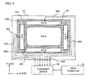
- FIG 4 is a diagram illustrating electrical connection configuration between the combiner 30 and the host computer 10. It is assumed that, for convenience of explanation, the lower left of a drawing is an original point, a transverse direction of the combiner 30 is an X-axis, and a longitudinal direction of the combiner 30 is a Y-axis.
- the electric field generation layer 34 having the electric field generation electrodes 341 and the insulating layers 342 is formed on the ground layer 32 as a pattern.
- the electric field generation electrodes 341 are illustrated by mesh patterns, and each of the insulating layers 342 illustrated with quadrangles is formed between the electric field generation electrodes 341 of the mesh patterns.
- the electric field generation electrodes 341 are connected to the judgment device 40 via a wiring 345.
- the ground layer 32 is connected to the judgment device 40 via a wiring 406.
- the electric field change output layer 36 is formed on an upper surface of the electric field generation layer 34.
- the electric field change output layer 36 includes five electric field detection electrodes RX0, RX1, RX2, RX3 and RX4 (hereinafter, referred to as a detection electrode). Since the combiner 30 is seen from above in FIG 4 , the electric field generation electrodes 341, the ground layer 32 and the detection electrodes RX0, RX1, RX2, RX3, and RX4 are illustrated on the same plane.
- the detection electrode RX0 is formed on a central domain of the combiner 30, and is connected to the judgment device 40 via a wiring 401.
- the detection electrode RX1 is formed on a left end of the X-axis of the combiner 30 illustrated in FIG 4 , and is connected to the judgment device 40 via a wiring 402.
- the detection electrode RX2 is formed on a right end of the X-axis of the combiner 30 illustrated in FIG 4 , and is connected to the judgment device 40 via a wiring 403.
- the detection electrode RX3 is formed on a top end of the Y-axis of the combiner 30 illustrated in FIG 4 , and is connected to the judgment device 40 via a wiring 404.
- the detection electrode RX4 is formed on a bottom end of the Y-axis of the combiner 30 illustrated in FIG 4 , and is connected to the judgment device 40 via a wiring 405.
- the insulating layers 39 are formed between the detection electrodes RX0, RX1, RX2, RX3 and RX4 of the electric field change output layer 36, respectively. That is, the electric field change output layer 36 includes the insulating layers 39 in addition to the detection electrodes RX0, RX1, RX2, RX3 and RX4.
- the voltage supply circuit 54 of the judgment device 40 is connected to the electric field generation electrodes 341 via the wiring 345, and supplies an alternating voltage to the electric field generation electrodes 341.
- the voltage supply circuit 54 supplies a pulse voltage of a square wave to the electric field generation electrode 341, for example.
- a voltage that is proportional to the alternating voltage supplied to the electric field generation electrode 341 and is smaller than the alternating voltage flows into each of the detection electrodes RX0, RX1, RX2, RX3 and RX4.
- the CPU 51 of the judgment device 40 judges the detection electrode which the finger of the operator approaches, based on a difference between a voltage supplied to the electric field generation electrodes 341 and a voltage outputted from each of the detection electrodes RX0, RX1, RX2, RX3 and RX4.
- the voltage outputted from each of the detection electrodes RX0, RX1, RX2, RX3 and RX4 reduces according to a distance between the finger which the operator brings close to the detection electrode, and each of the detection electrodes RX0, RX1, RX2, RX3 and RX4. The more the finger of the operator approaches any one of the detection electrodes, the larger the decrement of the voltage outputted from the detection electrode becomes.
- the CPU 51 generates a signal (hereinafter referred to as "a RX signal") according to a difference between the voltage supplied to the electric field generation electrodes 341 and the voltage outputted from each of the detection electrodes RX0, RX1, RX2, RX3 and RX4, and judges the gesture of the operator based on the generated RX signal.
- a RX signal a signal (hereinafter referred to as "a RX signal") according to a difference between the voltage supplied to the electric field generation electrodes 341 and the voltage outputted from each of the detection electrodes RX0, RX1, RX2, RX3 and RX4, and judges the gesture of the operator based on the generated RX signal.
- FIG 5A illustrates signal levels of the RX signals outputted from the respective detection electrodes which the judgment device 40 detects when the operator performs a gesture which moves the finger from a left end to a right end of the combiner 30.
- the finger passes the areas of the detection electrodes RX1, RX0 and RX2 in this order.
- the CPU 51 first detects a level of the RX signal based on a voltage inputted from the detection electrode RX1. Then, the CPU 51 detects a level of the RX signal based on a voltage inputted from the detection electrode RX0.
- the CPU 51 detects levels of the RX signals based on voltages inputted from the detection electrodes RX3 and RX4, respectively. This is because a distance between the finger and the area of the detection electrode RX3 and a distance between the finger and the area of the detection electrode RX4 become short. Finally, the CPU 51 detects a level of the RX signal inputted from the detection electrode RX2.
- FIG 5B illustrates signal levels of the RX signals which the judgment device 40 detects when the operator performs a gesture which moves the finger from the right end to the left end of the combiner 30. In the case of FIG 5B , contrary to the case of FIG 5A , the CPU 51 first detects the level of the RX signal from the detection electrode RX2.
- FIG 6A illustrates signal levels of the RX signals which the judgment device 40 detects when the operator performs a gesture which moves the finger from a bottom end to a top end of the combiner 30.
- the finger passes the areas of the detection electrodes RX4, RX0 and RX3 in this order.
- the CPU 51 first detects a level of the RX signal based on a voltage inputted from the detection electrode RX4. Then, the CPU 51 detects a level of the RX signal based on a voltage inputted from the detection electrode RX0.
- FIG 6B illustrates signal levels of the RX signals which the judgment device 40 detects when the operator performs a gesture which moves the finger from the top end to the bottom end of the combiner 30.
- the CPU 51 first detects the level of the RX signal from the detection electrode RX3.
- FIG 7A illustrates signal levels of the RX signals which the judgment device 40 detects when the finger of the operator approaches the combiner 30 in a vertical direction in the center of the area of the detection electrode RX0.
- the CPU 51 detects signal levels of the RX signals based on respective voltages of the detection electrodes RX0, RX1, RX2, RX3 and RX4. And, the level of the RX signal based on the voltage inputted from the detection electrode RX0 becomes a maximum value as the finger approaches the detection electrode RX0.
- FIG 7B illustrates signal levels of the RX signals which the judgment device 40 detects when the finger of the operator goes away from the combiner 30 in the vertical direction in the center of the area of the detection electrode RX0.
- the CPU 51 detects signal levels of the RX signals based on respective voltages of the detection electrodes RX0, RX1, RX2, RX3 and RX4. And, the level of the RX signal based on the voltage inputted from the detection electrode RX0 becomes a minimum value as the finger goes away from the detection electrode RX0.
- FIG 8A illustrates signal levels of the RX signals which the judgment device 40 detects when the operator performs circular motion of the finger on the areas of the detection electrodes RX3, RX2, RX4 and RX1 in this order.
- the CPU 51 first detects a level of the RX signal based on a voltage inputted from the detection electrode RX3. Next, the CPU 51 detects a level of the RX signal based on a voltage inputted from the detection electrode RX2. Then, the CPU 51 detects a level of the RX signal based on a voltage inputted from the detection electrode RX4. Finally, the CPU 51 detects a level of the RX signal based on a voltage inputted from the detection electrode RX1.
- FIG 8B illustrates signal levels of the RX signals which the judgment device 40 detects when the operator performs circular motion of the finger on the areas of the detection electrodes RX3, RX1, RX4 and RX2 in this order, i.e., in an opposite direction of FIG 8A .
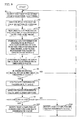
- the voltage supply circuit 54 of the judgment device 40 supplies a voltage to the electric field generation electrode 341 (step S1). Specifically, the voltage supply circuit 54 supplies the pulse voltage of the square wave to the electric field generation electrode 341.
- the voltage input circuit 55 of the judgment device 40 inputs an output voltage of each of the detection electrodes RX0, RX1, RX2, RX3 and RX4 (step S2).
- the CPU 51 of the judgment device 40 performs the filter process of the inputted voltage of each of the detection electrodes RX0, RX1, RX2, RX3 and RX4 to remove a noise (step S3).
- the CPU 51 performs AD-conversion of differences between the voltage supplied to the electric field generation electrode 341, and the filter-processed voltages to generate the RX signals (step S4).
- the CPU 51 compares the RX signals of the detection electrodes RX0, RX1, RX2, RX3 and RX4 with a threshold value (step S5).
- the threshold value is a value for judging whether each RX signal is an effective input, and is stored into the RAM 52 or the ROM 53 beforehand. The threshold value can be changed with the use of the host computer 10.
- the CPU 51 shifts to the process of step S7 when there is at least one RX signal equal to or more than the threshold value (YES in step S6), and the CPU 51 returns to the process of step S1 when there is no RX signal equal to or more than the threshold value (NO in step S6).
- the CPU 51 calculates coordinate values of X, Y and Z directions which indicate a position of the finger using the RX signals. It is assumed that, in this example, a horizontal direction of the combiner 30 illustrated in FIG 3 is set as an X-axis, a longitudinal direction of the combiner 30 is set as a Y-axis, and a vertical direction of the combiner 30 is set as a Z-axis.
- the coordinate values of X, Y and Z directions which indicate the position of the finger can be calculated by the following formulas (1), (2) and (3).
- "pp" indicates a peak signal.
- RX1pp means a signal in which a signal value indicates a peak among the RX signals detected by the detection electrode RX1.
- X RX ⁇ 1 ⁇ pp + RX ⁇ 2 ⁇ pp / 2
- X RX ⁇ 3 ⁇ pp + RX ⁇ 4 ⁇ pp / 2
- Z RX ⁇ 0 ⁇ pp
- the CPU 51 analyzes each coordinate value and judges whether the gesture is satisfied (step S8). Specifically, data which defines an order of change of the coordinate values is stored beforehand into the ROM 53 as judgment data for gesture. The CPU 51 judges whether the gesture is established based on whether the data which defines the order of change of the coordinate values is identical with an actual order of change of the coordinate values. It is assumed that the data which defines the order of change of the coordinate values includes a case where the coordinate values change in order of the detection electrodes RX1, RX0 and RX2, but does not include a case where the coordinate values change in order of the detection electrodes RX1, RX0 and RX1, for example.
- the CPU 51 judges that the gesture which moves the finger from the left end to the right end of the combiner 30 is established.
- the CPU 51 judges that the gesture is not established.
- step S9 the CPU 51 notifies the host computer 10 of the established gesture and the coordinate values of X, Y and Z (step S10). Also when the CPU 51 judges that the gesture is not established (NO in step S9), the CPU 51 notifies the host computer 10 of the coordinate values of X, Y and Z (step S11).
- the gesture which the operator inputs can be judged without separately providing an infrared sensor, a camera and the like to the head-up display 1. Therefore, enlargement of the head-up display 1 can be prevented and the manufacturing cost of the head-up display 1 can be reduced.
- the electric field change output layer 36 include five detection electrodes, the number of detection electrodes is not limited to this.
- the electric field change output layer 36 may include the detection electrodes of m rows ⁇ n columns (m and n are natural numbers equal to or more than 2).
Landscapes
- Engineering & Computer Science (AREA)
- General Engineering & Computer Science (AREA)
- Theoretical Computer Science (AREA)
- Physics & Mathematics (AREA)
- General Physics & Mathematics (AREA)
- Human Computer Interaction (AREA)
- Chemical & Material Sciences (AREA)
- Mechanical Engineering (AREA)
- Transportation (AREA)
- Combustion & Propulsion (AREA)
- Optics & Photonics (AREA)
- User Interface Of Digital Computer (AREA)
- Position Input By Displaying (AREA)
Abstract
Description
- The present invention relates to a combiner and an operation detection device.
- There has been known an input device which inputs operation information to display information displayed on a display screen, without removing an operator's sight line from the display screen. In the input device, gesture operation of the operator is captured with a camera, the captured moving image is analyzed, and an operation input by the operator is judged. Moreover, there has been known a technique that judges operation input by the operator by detecting gesture operation of the operator with an infrared sensor.
- There has been known an electrostatic capacitance type detection sensor as a sensor which detects operation input by the operator (see Japanese Laid-open Patent Publication No.
2010-92420 2010-182201 - However, when the gesture of the operator is judged with the camera and the infrared sensor, the camera and the infrared sensor must be provided separately, and hence the cost of a device becomes expensive and electrical power consumption becomes large. The judgment of the gesture using an image captured with the camera needs to perform complicated image analysis including a noise elimination technology of a disturbance light.
- Accordingly, it is desirable to provide a combiner that can input non-contact operation by an operator with a simple device configuration, and an operation detection device that can detect the non-contact operation by the operator with the simple device configuration.
- According to an aspect of the present invention, there is provided a combiner that reflects a light projected by a projector toward an operator, including: a reflection layer that reflects the light projected by the projector; an electric field generation layer that generates an electric field around the combiner; and an output layer that outputs a voltage according to change of the electric field generated by the field generation layer.
- According to another aspect of the present invention, there is provided an operation detection device including: a combiner that reflects a light projected by a projector toward an operator; and a judgment device; the combiner including: a reflection layer that reflects the light projected by the projector; an electric field generation layer that generates an electric field around the combiner; and an output layer that outputs a voltage according to change of the electric field generated by the field generation layer; and the judgment device including: a voltage supply circuit that supplies a voltage to the electric field generation layer; a voltage input circuit that inputs a voltage from the output layer; and a detector that detects a non-contact operation content by the operator based on a signal corresponding to a difference between the voltage supplied to the electric field generation layer and the voltage from the output layer.
-
-
FIG 1 is a diagram illustrating an example of the configuration of a head-up display; -
FIG 2 is a schematic diagram illustrating the configuration of a judgment device; -
FIG 3 is a cross-section diagram illustrating an example of the configuration of a combiner; -
FIG 4 is a diagram illustrating electrical connection configuration between the combiner and a host computer; -
FIG 5A is a diagram illustrating signal levels of RX signals which the judgment device detects when a gesture which moves a finger from left to right is performed; -
FIG 5B is a diagram illustrating signal levels of the RX signals which the judgment device detects when a gesture which moves the finger from right to left is performed; -
FIG 6A is a diagram illustrating signal levels of the RX signals which the judgment device detects when a gesture which moves the finger from bottom to top is performed; -
FIG 6B is a diagram illustrating signal levels of the RX signals which the judgment device detects when a gesture which moves the finger from top to bottom is performed; -
FIG 7A is a diagram illustrating signal levels of the RX signals which the judgment device detects when a gesture which brings the finger close to the combiner is performed; -
FIG 7B is a diagram illustrating signal levels of the RX signals which the judgment device detects when a gesture which goes away the finger from the combiner is performed; -
FIG 8A is a diagram illustrating signal levels of the RX signals which the judgment device detects when a gesture which rotates the finger in a clockwise direction is performed; -
FIG 8B is a diagram illustrating signal levels of the RX signals which the judgment device detects when a gesture which rotates the finger in a counterclockwise direction is performed; and -
FIG 9 is a flowchart illustrating a processing procedure of the judgment device. - A description will now be given of a preferable embodiment of the present invention with reference to the drawings.
- A description will be given of a head-up
display 1 with reference toFIG 1 . The head-updisplay 1 is a device which can directly project information on a human's view, projects information such as a projected image on a combiner including a hologram or a half mirror, and can show a virtual image to an operator as if the information floats in the air. The head-updisplay 1 is applied to a car navigation system mounted in a vehicle, or a medical information display system that displays a CT (Computed Tomographic) scanning image and an X-ray image. - The head-up
display 1 includes ahost computer 10, aprojector 20, acombiner 30, and ajudgment device 40. Thehost computer 10 supplies image data to theprojector 20. When the head-updisplay 1 is applied to a car navigation system mounted in a vehicle, for example, thehost computer 10 serves as a navigation device body. - The
projector 20 projects the image data supplied from thehost computer 10, toward thecombiner 30. When the head-updisplay 1 is mounted in the vehicle, for example, a traveling speed and various warning indication, or various data and map information that are intended to display based on various application prepared for beforehand are included in the image data. - The
combiner 30 penetrates a part of an incident light and reflects a remaining part of the incident light, so that it simultaneously leads an image which theprojector 20 projects and a natural light to operator's eyes. Thecombiner 30 has a so-called function of a half mirror. An example of the detailed configuration of thecombiner 30 is mentioned later. - The
judgment device 40 judges the operation such as the gesture of the operator, and outputs a judgment result to thehost computer 10.FIG 2 is a schematic diagram illustrating the configuration of thejudgment device 40. Thejudgment device 40 includes: aCPU 51 that controls the operation of the entire device; aRAM 52 that is a working memory; aROM 53 that stores programs and data; avoltage supply circuit 54 that supplies a voltage to thecombiner 30; avoltage input circuit 55 that inputs an output voltage from thecombiner 30; and a communication interface (I/F) 56 that communicates with thehost computer 10. TheCPU 51 is connected to theRAM 52, theROM 53, thevoltage supply circuit 54, thevoltage input circuit 55 and the communication I/F 56. Thevoltage input circuit 55 includes a ground terminal, not shown. TheCPU 51 performs a filter process, an A/D conversion process and so on as mentioned later to a voltage signal (an output voltage) inputted from thecombiner 30 via thevoltage input circuit 55. Here, inFIG 1 , thehost computer 10 and thejudgment device 40 are provided as discrete devices, but thejudgment device 40 may be achieved by thehost computer 10. - Next, a description will be given of an example of the detailed configuration of the
combiner 30 with reference toFIG 3. FIG 3 is a cross-section diagram illustrating an example of the configuration of thecombiner 30. An upper side ofFIG 3 is an operator side. Thecombiner 30 includes a firstinterference fringe layer 31, aground layer 32, a secondinterference fringe layer 33, an electricfield generation layer 34, a thirdinterference fringe layer 35, an electric fieldchange output layer 36, and a fourthinterference fringe layer 37. The electricfield generation layer 34 includes electricfield generation electrodes 341 andinsulating layers 342. The electric fieldchange output layer 36 includes a plurality of electric field detection electrodes mentioned later. - Each of the first
interference fringe layer 31, the secondinterference fringe layer 33, the thirdinterference fringe layer 35 and the fourthinterference fringe layer 37 which functions as a reflection layer penetrates a part of the incident light and reflects the image projected from theprojector 20. Here, the combiner does not necessarily need to have four interference fringe layers. It is desirable that the combiner has at least two interference fringe layers. Moreover, instead of the interference fringe layer, a certain reflection layer having a function that penetrates a part of the incident light and reflects the image from theprojector 20 may be provided. When the electric fieldchange output layer 36 is too near the electricfield generation layer 34, it is easy to generate a noise on a voltage which thejudgment device 40 inputs from the electricfield generation layer 34. Therefore, it is desirable that the interference fringe layer (i.e., the third interference fringe layer 35) is provided between the electricfield generation layer 34 and the electric fieldchange output layer 36. Here, instead of a part of the interference fringe layers and the reflection layers, a layer having a function that penetrates the light may be provided. -
FIG 4 is a diagram illustrating electrical connection configuration between thecombiner 30 and thehost computer 10. It is assumed that, for convenience of explanation, the lower left of a drawing is an original point, a transverse direction of thecombiner 30 is an X-axis, and a longitudinal direction of thecombiner 30 is a Y-axis. In thecombiner 30 illustrated inFIG. 4 , the electricfield generation layer 34 having the electricfield generation electrodes 341 and theinsulating layers 342 is formed on theground layer 32 as a pattern. Here, inFIG 4 , the electricfield generation electrodes 341 are illustrated by mesh patterns, and each of theinsulating layers 342 illustrated with quadrangles is formed between the electricfield generation electrodes 341 of the mesh patterns. The electricfield generation electrodes 341 are connected to thejudgment device 40 via awiring 345. Theground layer 32 is connected to thejudgment device 40 via awiring 406. - Moreover, the electric field
change output layer 36 is formed on an upper surface of the electricfield generation layer 34. The electric fieldchange output layer 36 includes five electric field detection electrodes RX0, RX1, RX2, RX3 and RX4 (hereinafter, referred to as a detection electrode). Since thecombiner 30 is seen from above inFIG 4 , the electricfield generation electrodes 341, theground layer 32 and the detection electrodes RX0, RX1, RX2, RX3, and RX4 are illustrated on the same plane. The detection electrode RX0 is formed on a central domain of thecombiner 30, and is connected to thejudgment device 40 via awiring 401. The detection electrode RX1 is formed on a left end of the X-axis of thecombiner 30 illustrated inFIG 4 , and is connected to thejudgment device 40 via awiring 402. The detection electrode RX2 is formed on a right end of the X-axis of thecombiner 30 illustrated inFIG 4 , and is connected to thejudgment device 40 via awiring 403. The detection electrode RX3 is formed on a top end of the Y-axis of thecombiner 30 illustrated inFIG 4 , and is connected to thejudgment device 40 via awiring 404. The detection electrode RX4 is formed on a bottom end of the Y-axis of thecombiner 30 illustrated inFIG 4 , and is connected to thejudgment device 40 via awiring 405. The insulating layers 39 are formed between the detection electrodes RX0, RX1, RX2, RX3 and RX4 of the electric fieldchange output layer 36, respectively. That is, the electric fieldchange output layer 36 includes the insulatinglayers 39 in addition to the detection electrodes RX0, RX1, RX2, RX3 and RX4. - The
voltage supply circuit 54 of thejudgment device 40 is connected to the electricfield generation electrodes 341 via thewiring 345, and supplies an alternating voltage to the electricfield generation electrodes 341. Thevoltage supply circuit 54 supplies a pulse voltage of a square wave to the electricfield generation electrode 341, for example. A voltage that is proportional to the alternating voltage supplied to the electricfield generation electrode 341 and is smaller than the alternating voltage flows into each of the detection electrodes RX0, RX1, RX2, RX3 and RX4. When the finger of the operator with the role of a ground is brought close to any one of the detection electrodes RX0, RX1, RX2, RX3 and RX4, an electric field near an electrode to which the finger is brought close is changed, and a voltage detected with the detection electrode to which the finger is brought close is reduced. - The
CPU 51 of thejudgment device 40 judges the detection electrode which the finger of the operator approaches, based on a difference between a voltage supplied to the electricfield generation electrodes 341 and a voltage outputted from each of the detection electrodes RX0, RX1, RX2, RX3 and RX4. The voltage outputted from each of the detection electrodes RX0, RX1, RX2, RX3 and RX4 reduces according to a distance between the finger which the operator brings close to the detection electrode, and each of the detection electrodes RX0, RX1, RX2, RX3 and RX4. The more the finger of the operator approaches any one of the detection electrodes, the larger the decrement of the voltage outputted from the detection electrode becomes. TheCPU 51 generates a signal (hereinafter referred to as "a RX signal") according to a difference between the voltage supplied to the electricfield generation electrodes 341 and the voltage outputted from each of the detection electrodes RX0, RX1, RX2, RX3 and RX4, and judges the gesture of the operator based on the generated RX signal. -
FIG 5A illustrates signal levels of the RX signals outputted from the respective detection electrodes which thejudgment device 40 detects when the operator performs a gesture which moves the finger from a left end to a right end of thecombiner 30. Here, it is assumed that the finger passes the areas of the detection electrodes RX1, RX0 and RX2 in this order. In this case, theCPU 51 first detects a level of the RX signal based on a voltage inputted from the detection electrode RX1. Then, theCPU 51 detects a level of the RX signal based on a voltage inputted from the detection electrode RX0. Here, when the position of the finger moves to the area of the detection electrode RX0, theCPU 51 detects levels of the RX signals based on voltages inputted from the detection electrodes RX3 and RX4, respectively. This is because a distance between the finger and the area of the detection electrode RX3 and a distance between the finger and the area of the detection electrode RX4 become short. Finally, theCPU 51 detects a level of the RX signal inputted from the detection electrode RX2.FIG 5B illustrates signal levels of the RX signals which thejudgment device 40 detects when the operator performs a gesture which moves the finger from the right end to the left end of thecombiner 30. In the case ofFIG 5B , contrary to the case ofFIG 5A , theCPU 51 first detects the level of the RX signal from the detection electrode RX2. -
FIG 6A illustrates signal levels of the RX signals which thejudgment device 40 detects when the operator performs a gesture which moves the finger from a bottom end to a top end of thecombiner 30. Here, it is assumed that the finger passes the areas of the detection electrodes RX4, RX0 and RX3 in this order. In this case, theCPU 51 first detects a level of the RX signal based on a voltage inputted from the detection electrode RX4. Then, theCPU 51 detects a level of the RX signal based on a voltage inputted from the detection electrode RX0. Here, when the position of the finger moves to the area of the detection electrode RX0, theCPU 51 detects levels of the RX signals based on voltages inputted from the detection electrodes RX1 and RX2, respectively. Finally, theCPU 51 detects a level of the RX signal inputted from the detection electrode RX3.FIG 6B illustrates signal levels of the RX signals which thejudgment device 40 detects when the operator performs a gesture which moves the finger from the top end to the bottom end of thecombiner 30. In the case ofFIG 6B , contrary to the case ofFIG 6A , theCPU 51 first detects the level of the RX signal from the detection electrode RX3. -
FIG 7A illustrates signal levels of the RX signals which thejudgment device 40 detects when the finger of the operator approaches thecombiner 30 in a vertical direction in the center of the area of the detection electrode RX0. In this case, theCPU 51 detects signal levels of the RX signals based on respective voltages of the detection electrodes RX0, RX1, RX2, RX3 and RX4. And, the level of the RX signal based on the voltage inputted from the detection electrode RX0 becomes a maximum value as the finger approaches the detection electrode RX0. -
FIG 7B illustrates signal levels of the RX signals which thejudgment device 40 detects when the finger of the operator goes away from thecombiner 30 in the vertical direction in the center of the area of the detection electrode RX0. In this case, theCPU 51 detects signal levels of the RX signals based on respective voltages of the detection electrodes RX0, RX1, RX2, RX3 and RX4. And, the level of the RX signal based on the voltage inputted from the detection electrode RX0 becomes a minimum value as the finger goes away from the detection electrode RX0. -
FIG 8A illustrates signal levels of the RX signals which thejudgment device 40 detects when the operator performs circular motion of the finger on the areas of the detection electrodes RX3, RX2, RX4 and RX1 in this order. In this case, theCPU 51 first detects a level of the RX signal based on a voltage inputted from the detection electrode RX3. Next, theCPU 51 detects a level of the RX signal based on a voltage inputted from the detection electrode RX2. Then, theCPU 51 detects a level of the RX signal based on a voltage inputted from the detection electrode RX4. Finally, theCPU 51 detects a level of the RX signal based on a voltage inputted from the detection electrode RX1. Here, since the finger does not pass the area of the detection electrodes RX0, the level of the RX signal based on the voltage inputted from the detection electrode RX0 is smaller than the signal levels of the detection electrodes RX3, RX2, RX4 and RX1. Here,FIG 8B illustrates signal levels of the RX signals which thejudgment device 40 detects when the operator performs circular motion of the finger on the areas of the detection electrodes RX3, RX1, RX4 and RX2 in this order, i.e., in an opposite direction ofFIG 8A . - Next, a description will be given of a processing procedure of the judgment device with reference to a flowchart illustrated in
FIG 9 . First, thevoltage supply circuit 54 of thejudgment device 40 supplies a voltage to the electric field generation electrode 341 (step S1). Specifically, thevoltage supply circuit 54 supplies the pulse voltage of the square wave to the electricfield generation electrode 341. Thevoltage input circuit 55 of thejudgment device 40 inputs an output voltage of each of the detection electrodes RX0, RX1, RX2, RX3 and RX4 (step S2). Next, theCPU 51 of thejudgment device 40 performs the filter process of the inputted voltage of each of the detection electrodes RX0, RX1, RX2, RX3 and RX4 to remove a noise (step S3). TheCPU 51 performs AD-conversion of differences between the voltage supplied to the electricfield generation electrode 341, and the filter-processed voltages to generate the RX signals (step S4). Next, theCPU 51 compares the RX signals of the detection electrodes RX0, RX1, RX2, RX3 and RX4 with a threshold value (step S5). The threshold value is a value for judging whether each RX signal is an effective input, and is stored into theRAM 52 or theROM 53 beforehand. The threshold value can be changed with the use of thehost computer 10. TheCPU 51 shifts to the process of step S7 when there is at least one RX signal equal to or more than the threshold value (YES in step S6), and theCPU 51 returns to the process of step S1 when there is no RX signal equal to or more than the threshold value (NO in step S6). - In the process of step S7, the
CPU 51 calculates coordinate values of X, Y and Z directions which indicate a position of the finger using the RX signals. It is assumed that, in this example, a horizontal direction of thecombiner 30 illustrated inFIG 3 is set as an X-axis, a longitudinal direction of thecombiner 30 is set as a Y-axis, and a vertical direction of thecombiner 30 is set as a Z-axis. Here, the coordinate values of X, Y and Z directions which indicate the position of the finger can be calculated by the following formulas (1), (2) and (3). Here, in the formulas (1), (2) and (3), "pp" indicates a peak signal. For example, "RX1pp" means a signal in which a signal value indicates a peak among the RX signals detected by the detection electrode RX1.
[Formula 1]
[Formula 2]
[Formula 3]
- Next, the
CPU 51 analyzes each coordinate value and judges whether the gesture is satisfied (step S8). Specifically, data which defines an order of change of the coordinate values is stored beforehand into theROM 53 as judgment data for gesture. TheCPU 51 judges whether the gesture is established based on whether the data which defines the order of change of the coordinate values is identical with an actual order of change of the coordinate values. It is assumed that the data which defines the order of change of the coordinate values includes a case where the coordinate values change in order of the detection electrodes RX1, RX0 and RX2, but does not include a case where the coordinate values change in order of the detection electrodes RX1, RX0 and RX1, for example. In this case, when the coordinate values change in order of the detection electrodes RX1, RX0 and RX2, theCPU 51 judges that the gesture which moves the finger from the left end to the right end of thecombiner 30 is established. On the other hand, when the coordinate values change in order of the detection electrodes RX1, RX0 and RX1, theCPU 51 judges that the gesture is not established. - When the
CPU 51 judges that the gesture is established (YES in step S9), theCPU 51 notifies thehost computer 10 of the established gesture and the coordinate values of X, Y and Z (step S10). Also when theCPU 51 judges that the gesture is not established (NO in step S9), theCPU 51 notifies thehost computer 10 of the coordinate values of X, Y and Z (step S11). - As described above, according to the present embodiment, the gesture which the operator inputs can be judged without separately providing an infrared sensor, a camera and the like to the head-up
display 1. Therefore, enlargement of the head-updisplay 1 can be prevented and the manufacturing cost of the head-updisplay 1 can be reduced. - Although in the above-mentioned embodiment, the electric field
change output layer 36 include five detection electrodes, the number of detection electrodes is not limited to this. For example, the electric fieldchange output layer 36 may include the detection electrodes of m rows × n columns (m and n are natural numbers equal to or more than 2). - The above-mentioned embodiment is a preferable embodiment of the present invention. However, the present invention is not limited to the specifically disclosed embodiment and variations but may include other embodiments and variations without departing from the scope of the present invention.
Claims (5)
- A combiner (30) that reflects a light projected by a projector (20) toward an operator, comprising:a reflection layer (31, 33, 35, 37) that reflects the light projected by the projector;an electric field generation layer (34) that generates an electric field around the combiner; andan output layer (36) that outputs a voltage according to change of the electric field generated by the field generation layer.
- The combiner as claimed in claim 1, comprising:a plurality of reflection layers (31, 33, 35, 37);wherein a single reflection layer among the plurality of reflection layers is arranged between the field generation layer and the output layer
- The combiner as claimed in claim 1 or 2, wherein
the output layer includes a plurality of electrodes (341), a single electrode is arranged in the center of the output layer, and other electrodes are arranged at front, rear, right and left of the single electrode via insulating layers (342). - An operation detection device, comprising:a combiner (30) that reflects a light projected by a projector toward an operator; anda judgment device (40);the combiner including:a reflection layer (31, 33, 35, 37) that reflects the light projected by the projector;an electric field generation layer (34) that generates an electric field around the combiner; andan output layer (36) that outputs a voltage according to change of the electric field generated by the field generation layer; andthe judgment device including:a voltage supply circuit (54) that supplies a voltage to the electric field generation layer;a voltage input circuit (55) that inputs a voltage from the output layer; anda detector (51) that detects a non-contact operation content by the operator based on a signal corresponding to a difference between the voltage supplied to the electric field generation layer and the voltage from the output layer.
- The operation detection device as claimed in claim 4, wherein
the output layer includes a plurality of electrodes (RX0, RX1, RX2, RX3, RX4), and the detector detects the non-contact operation content of a gesture by the operator based on judgment data for gesture, and a signal corresponding to a difference between the voltage supplied to the electric field generation layer and a voltage from each of the plurality of electrodes.
Applications Claiming Priority (1)
| Application Number | Priority Date | Filing Date | Title |
|---|---|---|---|
| JP2013198999A JP6174435B2 (en) | 2013-09-25 | 2013-09-25 | Combiner and operation detection device |
Publications (2)
| Publication Number | Publication Date |
|---|---|
| EP2853987A1 true EP2853987A1 (en) | 2015-04-01 |
| EP2853987B1 EP2853987B1 (en) | 2018-02-21 |
Family
ID=51564455
Family Applications (1)
| Application Number | Title | Priority Date | Filing Date |
|---|---|---|---|
| EP14183915.9A Active EP2853987B1 (en) | 2013-09-25 | 2014-09-08 | Head up display with non contact gesture detection. |
Country Status (5)
| Country | Link |
|---|---|
| US (1) | US9939906B2 (en) |
| EP (1) | EP2853987B1 (en) |
| JP (1) | JP6174435B2 (en) |
| CN (1) | CN104461123B (en) |
| TW (1) | TWI609291B (en) |
Families Citing this family (1)
| Publication number | Priority date | Publication date | Assignee | Title |
|---|---|---|---|---|
| CN107807778A (en) * | 2017-11-07 | 2018-03-16 | 深圳创维-Rgb电子有限公司 | A kind of control method of display system and display system |
Citations (5)
| Publication number | Priority date | Publication date | Assignee | Title |
|---|---|---|---|---|
| JP2010092420A (en) | 2008-10-10 | 2010-04-22 | Sony Corp | Information processing apparatus, method and system, and program for processing information |
| JP2010182201A (en) | 2009-02-06 | 2010-08-19 | Hitachi Ltd | Capacitive sensor |
| DE102009046376A1 (en) * | 2009-11-04 | 2011-05-05 | Robert Bosch Gmbh | Driver assistance system for automobile, has input device including manually operated control element that is arranged at steering wheel and/or in area of instrument panel, where area lies in direct vicinity of wheel |
| US20120105370A1 (en) * | 2005-12-12 | 2012-05-03 | Nupix, LLC | Electroded Sheet for a Multitude of Products |
| US20120173067A1 (en) * | 2010-12-30 | 2012-07-05 | GM Global Technology Operations LLC | Graphical vehicle command system for autonomous vehicles on full windshield head-up display |
Family Cites Families (12)
| Publication number | Priority date | Publication date | Assignee | Title |
|---|---|---|---|---|
| JPH04362426A (en) * | 1991-06-07 | 1992-12-15 | Omron Corp | Head up display unit |
| US5859714A (en) * | 1993-11-16 | 1999-01-12 | Asahi Glass Company, Ltd. | Head-up display, a combiner used for the head-up display and a method of designing the head-up display |
| JPH0876050A (en) * | 1994-09-05 | 1996-03-22 | Fujitsu Ten Ltd | Display device for vehicle |
| JP2005138755A (en) * | 2003-11-07 | 2005-06-02 | Denso Corp | Device and program for displaying virtual images |
| JP4268191B2 (en) | 2004-12-14 | 2009-05-27 | パナソニック株式会社 | Information presenting apparatus, information presenting method, program, and recording medium |
| DE102007016408A1 (en) * | 2007-03-26 | 2008-10-02 | Ident Technology Ag | Mobile communication device and input device therefor |
| DE102008057823A1 (en) | 2008-11-18 | 2010-08-19 | Ident Technology Ag | Capacitive sensor system |
| JP2010244132A (en) * | 2009-04-01 | 2010-10-28 | Mitsubishi Electric Corp | User interface device with touch panel, method and program for controlling user interface |
| DE102011010919B4 (en) * | 2010-02-10 | 2018-05-09 | Microchip Technology Germany Gmbh | System and method for generating a signal correlated with a manual input operation |
| US9292093B2 (en) * | 2010-11-18 | 2016-03-22 | Alpine Electronics, Inc. | Interface method and apparatus for inputting information with air finger gesture |
| US8860690B2 (en) * | 2011-12-15 | 2014-10-14 | Atmel Corporation | Touch sensor with capacitive nodes having a capacitance that is approximately the same |
| WO2013100325A1 (en) | 2011-12-28 | 2013-07-04 | 엘지전자 주식회사 | Mobile terminal |
-
2013
- 2013-09-25 JP JP2013198999A patent/JP6174435B2/en active Active
-
2014
- 2014-08-26 US US14/468,427 patent/US9939906B2/en active Active
- 2014-09-08 EP EP14183915.9A patent/EP2853987B1/en active Active
- 2014-09-25 TW TW103133335A patent/TWI609291B/en active
- 2014-09-25 CN CN201410496141.7A patent/CN104461123B/en active Active
Patent Citations (5)
| Publication number | Priority date | Publication date | Assignee | Title |
|---|---|---|---|---|
| US20120105370A1 (en) * | 2005-12-12 | 2012-05-03 | Nupix, LLC | Electroded Sheet for a Multitude of Products |
| JP2010092420A (en) | 2008-10-10 | 2010-04-22 | Sony Corp | Information processing apparatus, method and system, and program for processing information |
| JP2010182201A (en) | 2009-02-06 | 2010-08-19 | Hitachi Ltd | Capacitive sensor |
| DE102009046376A1 (en) * | 2009-11-04 | 2011-05-05 | Robert Bosch Gmbh | Driver assistance system for automobile, has input device including manually operated control element that is arranged at steering wheel and/or in area of instrument panel, where area lies in direct vicinity of wheel |
| US20120173067A1 (en) * | 2010-12-30 | 2012-07-05 | GM Global Technology Operations LLC | Graphical vehicle command system for autonomous vehicles on full windshield head-up display |
Non-Patent Citations (1)
| Title |
|---|
| SHAHRAM IZADI ET AL: "ThinSight: A Thin Form-Factor Interactive Surface Technology", COMMUNICATIONS OF THE ACM, vol. 52, no. 12, 1 December 2009 (2009-12-01), pages 90, XP055138679, ISSN: 0001-0782, DOI: 10.1145/1610252.1610277 * |
Also Published As
| Publication number | Publication date |
|---|---|
| JP2015064799A (en) | 2015-04-09 |
| EP2853987B1 (en) | 2018-02-21 |
| CN104461123A (en) | 2015-03-25 |
| JP6174435B2 (en) | 2017-08-02 |
| TWI609291B (en) | 2017-12-21 |
| TW201512902A (en) | 2015-04-01 |
| US20150084856A1 (en) | 2015-03-26 |
| US9939906B2 (en) | 2018-04-10 |
| CN104461123B (en) | 2017-08-22 |
Similar Documents
| Publication | Publication Date | Title |
|---|---|---|
| EP3652703B1 (en) | Visual, depth and micro-vibration data extraction using a unified imaging device | |
| CN110770686B (en) | Sensor for detecting pen signal sent by pen | |
| EP2966555B1 (en) | Three-dimensional operation control method and device for touchscreen, and mobile terminal thereof | |
| US20090183931A1 (en) | Touch panel device | |
| US20140118533A1 (en) | Operational stability enhancing device for construction machinery | |
| US10317999B2 (en) | Vibrotactile driver circuit for haptic devices | |
| US10156927B2 (en) | Operation detecting device for detecting the presence of a foreign object on an operation surface | |
| US11032479B2 (en) | Bird's-eye view video generation device, bird's-eye view video generation method, and non-transitory storage medium | |
| CN114041284B (en) | System, information processing apparatus, information processing method, and computer readable medium | |
| JP6441581B2 (en) | Light detection for bending motion of flexible display | |
| US9495046B2 (en) | Parasitic capacitance filter for single-layer capacitive imaging sensors | |
| CN112739976A (en) | Dimension measuring device and dimension measuring method | |
| CN116567399A (en) | Peripheral inspection device | |
| US20180329532A1 (en) | Operation detection device | |
| EP2853987A1 (en) | Head up display with non contact gesture detection | |
| CN108422932A (en) | driving assistance system, method and vehicle | |
| US9612681B2 (en) | 3D display apparatus and control method for same | |
| US9753563B2 (en) | Manipulation apparatus and manipulation teaching method for manipulation apparatus | |
| JP2015082300A (en) | Display input device | |
| JP6169446B2 (en) | Gaze detection device | |
| US11073937B2 (en) | Capacitive interface device with mixed electrode structure, and apparatus comprising the device | |
| KR101888362B1 (en) | Terrain guidance device and method using 3D reconstruction | |
| JP7265878B2 (en) | input device | |
| US11221711B2 (en) | Input control device, input control method and display device that estimate operator position relative to a touch panel | |
| JP2017083986A (en) | Operation input device |
Legal Events
| Date | Code | Title | Description |
|---|---|---|---|
| PUAI | Public reference made under article 153(3) epc to a published international application that has entered the european phase |
Free format text: ORIGINAL CODE: 0009012 |
|
| 17P | Request for examination filed |
Effective date: 20140908 |
|
| AK | Designated contracting states |
Kind code of ref document: A1 Designated state(s): AL AT BE BG CH CY CZ DE DK EE ES FI FR GB GR HR HU IE IS IT LI LT LU LV MC MK MT NL NO PL PT RO RS SE SI SK SM TR |
|
| AX | Request for extension of the european patent |
Extension state: BA ME |
|
| R17P | Request for examination filed (corrected) |
Effective date: 20150811 |
|
| RBV | Designated contracting states (corrected) |
Designated state(s): AL AT BE BG CH CY CZ DE DK EE ES FI FR GB GR HR HU IE IS IT LI LT LU LV MC MK MT NL NO PL PT RO RS SE SI SK SM TR |
|
| STAA | Information on the status of an ep patent application or granted ep patent |
Free format text: STATUS: EXAMINATION IS IN PROGRESS |
|
| 17Q | First examination report despatched |
Effective date: 20170124 |
|
| GRAP | Despatch of communication of intention to grant a patent |
Free format text: ORIGINAL CODE: EPIDOSNIGR1 |
|
| STAA | Information on the status of an ep patent application or granted ep patent |
Free format text: STATUS: GRANT OF PATENT IS INTENDED |
|
| INTG | Intention to grant announced |
Effective date: 20170829 |
|
| GRAS | Grant fee paid |
Free format text: ORIGINAL CODE: EPIDOSNIGR3 |
|
| GRAA | (expected) grant |
Free format text: ORIGINAL CODE: 0009210 |
|
| STAA | Information on the status of an ep patent application or granted ep patent |
Free format text: STATUS: THE PATENT HAS BEEN GRANTED |
|
| AK | Designated contracting states |
Kind code of ref document: B1 Designated state(s): AL AT BE BG CH CY CZ DE DK EE ES FI FR GB GR HR HU IE IS IT LI LT LU LV MC MK MT NL NO PL PT RO RS SE SI SK SM TR |
|
| REG | Reference to a national code |
Ref country code: GB Ref legal event code: FG4D |
|
| REG | Reference to a national code |
Ref country code: CH Ref legal event code: EP |
|
| REG | Reference to a national code |
Ref country code: AT Ref legal event code: REF Ref document number: 972418 Country of ref document: AT Kind code of ref document: T Effective date: 20180315 |
|
| REG | Reference to a national code |
Ref country code: IE Ref legal event code: FG4D |
|
| REG | Reference to a national code |
Ref country code: DE Ref legal event code: R096 Ref document number: 602014021130 Country of ref document: DE |
|
| REG | Reference to a national code |
Ref country code: NL Ref legal event code: MP Effective date: 20180221 |
|
| REG | Reference to a national code |
Ref country code: LT Ref legal event code: MG4D |
|
| REG | Reference to a national code |
Ref country code: AT Ref legal event code: MK05 Ref document number: 972418 Country of ref document: AT Kind code of ref document: T Effective date: 20180221 |
|
| PG25 | Lapsed in a contracting state [announced via postgrant information from national office to epo] |
Ref country code: HR Free format text: LAPSE BECAUSE OF FAILURE TO SUBMIT A TRANSLATION OF THE DESCRIPTION OR TO PAY THE FEE WITHIN THE PRESCRIBED TIME-LIMIT Effective date: 20180221 Ref country code: NL Free format text: LAPSE BECAUSE OF FAILURE TO SUBMIT A TRANSLATION OF THE DESCRIPTION OR TO PAY THE FEE WITHIN THE PRESCRIBED TIME-LIMIT Effective date: 20180221 Ref country code: LT Free format text: LAPSE BECAUSE OF FAILURE TO SUBMIT A TRANSLATION OF THE DESCRIPTION OR TO PAY THE FEE WITHIN THE PRESCRIBED TIME-LIMIT Effective date: 20180221 Ref country code: FI Free format text: LAPSE BECAUSE OF FAILURE TO SUBMIT A TRANSLATION OF THE DESCRIPTION OR TO PAY THE FEE WITHIN THE PRESCRIBED TIME-LIMIT Effective date: 20180221 Ref country code: ES Free format text: LAPSE BECAUSE OF FAILURE TO SUBMIT A TRANSLATION OF THE DESCRIPTION OR TO PAY THE FEE WITHIN THE PRESCRIBED TIME-LIMIT Effective date: 20180221 Ref country code: NO Free format text: LAPSE BECAUSE OF FAILURE TO SUBMIT A TRANSLATION OF THE DESCRIPTION OR TO PAY THE FEE WITHIN THE PRESCRIBED TIME-LIMIT Effective date: 20180521 Ref country code: CY Free format text: LAPSE BECAUSE OF FAILURE TO SUBMIT A TRANSLATION OF THE DESCRIPTION OR TO PAY THE FEE WITHIN THE PRESCRIBED TIME-LIMIT Effective date: 20180221 |
|
| PG25 | Lapsed in a contracting state [announced via postgrant information from national office to epo] |
Ref country code: AT Free format text: LAPSE BECAUSE OF FAILURE TO SUBMIT A TRANSLATION OF THE DESCRIPTION OR TO PAY THE FEE WITHIN THE PRESCRIBED TIME-LIMIT Effective date: 20180221 Ref country code: LV Free format text: LAPSE BECAUSE OF FAILURE TO SUBMIT A TRANSLATION OF THE DESCRIPTION OR TO PAY THE FEE WITHIN THE PRESCRIBED TIME-LIMIT Effective date: 20180221 Ref country code: SE Free format text: LAPSE BECAUSE OF FAILURE TO SUBMIT A TRANSLATION OF THE DESCRIPTION OR TO PAY THE FEE WITHIN THE PRESCRIBED TIME-LIMIT Effective date: 20180221 Ref country code: RS Free format text: LAPSE BECAUSE OF FAILURE TO SUBMIT A TRANSLATION OF THE DESCRIPTION OR TO PAY THE FEE WITHIN THE PRESCRIBED TIME-LIMIT Effective date: 20180221 Ref country code: GR Free format text: LAPSE BECAUSE OF FAILURE TO SUBMIT A TRANSLATION OF THE DESCRIPTION OR TO PAY THE FEE WITHIN THE PRESCRIBED TIME-LIMIT Effective date: 20180522 Ref country code: BG Free format text: LAPSE BECAUSE OF FAILURE TO SUBMIT A TRANSLATION OF THE DESCRIPTION OR TO PAY THE FEE WITHIN THE PRESCRIBED TIME-LIMIT Effective date: 20180521 |
|
| REG | Reference to a national code |
Ref country code: FR Ref legal event code: PLFP Year of fee payment: 5 |
|
| PG25 | Lapsed in a contracting state [announced via postgrant information from national office to epo] |
Ref country code: AL Free format text: LAPSE BECAUSE OF FAILURE TO SUBMIT A TRANSLATION OF THE DESCRIPTION OR TO PAY THE FEE WITHIN THE PRESCRIBED TIME-LIMIT Effective date: 20180221 Ref country code: IT Free format text: LAPSE BECAUSE OF FAILURE TO SUBMIT A TRANSLATION OF THE DESCRIPTION OR TO PAY THE FEE WITHIN THE PRESCRIBED TIME-LIMIT Effective date: 20180221 Ref country code: PL Free format text: LAPSE BECAUSE OF FAILURE TO SUBMIT A TRANSLATION OF THE DESCRIPTION OR TO PAY THE FEE WITHIN THE PRESCRIBED TIME-LIMIT Effective date: 20180221 Ref country code: EE Free format text: LAPSE BECAUSE OF FAILURE TO SUBMIT A TRANSLATION OF THE DESCRIPTION OR TO PAY THE FEE WITHIN THE PRESCRIBED TIME-LIMIT Effective date: 20180221 Ref country code: RO Free format text: LAPSE BECAUSE OF FAILURE TO SUBMIT A TRANSLATION OF THE DESCRIPTION OR TO PAY THE FEE WITHIN THE PRESCRIBED TIME-LIMIT Effective date: 20180221 |
|
| REG | Reference to a national code |
Ref country code: DE Ref legal event code: R097 Ref document number: 602014021130 Country of ref document: DE |
|
| PG25 | Lapsed in a contracting state [announced via postgrant information from national office to epo] |
Ref country code: SK Free format text: LAPSE BECAUSE OF FAILURE TO SUBMIT A TRANSLATION OF THE DESCRIPTION OR TO PAY THE FEE WITHIN THE PRESCRIBED TIME-LIMIT Effective date: 20180221 Ref country code: CZ Free format text: LAPSE BECAUSE OF FAILURE TO SUBMIT A TRANSLATION OF THE DESCRIPTION OR TO PAY THE FEE WITHIN THE PRESCRIBED TIME-LIMIT Effective date: 20180221 Ref country code: SM Free format text: LAPSE BECAUSE OF FAILURE TO SUBMIT A TRANSLATION OF THE DESCRIPTION OR TO PAY THE FEE WITHIN THE PRESCRIBED TIME-LIMIT Effective date: 20180221 Ref country code: DK Free format text: LAPSE BECAUSE OF FAILURE TO SUBMIT A TRANSLATION OF THE DESCRIPTION OR TO PAY THE FEE WITHIN THE PRESCRIBED TIME-LIMIT Effective date: 20180221 |
|
| PLBE | No opposition filed within time limit |
Free format text: ORIGINAL CODE: 0009261 |
|
| STAA | Information on the status of an ep patent application or granted ep patent |
Free format text: STATUS: NO OPPOSITION FILED WITHIN TIME LIMIT |
|
| 26N | No opposition filed |
Effective date: 20181122 |
|
| PG25 | Lapsed in a contracting state [announced via postgrant information from national office to epo] |
Ref country code: SI Free format text: LAPSE BECAUSE OF FAILURE TO SUBMIT A TRANSLATION OF THE DESCRIPTION OR TO PAY THE FEE WITHIN THE PRESCRIBED TIME-LIMIT Effective date: 20180221 |
|
| PG25 | Lapsed in a contracting state [announced via postgrant information from national office to epo] |
Ref country code: MC Free format text: LAPSE BECAUSE OF FAILURE TO SUBMIT A TRANSLATION OF THE DESCRIPTION OR TO PAY THE FEE WITHIN THE PRESCRIBED TIME-LIMIT Effective date: 20180221 |
|
| REG | Reference to a national code |
Ref country code: CH Ref legal event code: PL |
|
| REG | Reference to a national code |
Ref country code: BE Ref legal event code: MM Effective date: 20180930 |
|
| REG | Reference to a national code |
Ref country code: IE Ref legal event code: MM4A |
|
| PG25 | Lapsed in a contracting state [announced via postgrant information from national office to epo] |
Ref country code: LU Free format text: LAPSE BECAUSE OF NON-PAYMENT OF DUE FEES Effective date: 20180908 |
|
| PG25 | Lapsed in a contracting state [announced via postgrant information from national office to epo] |
Ref country code: IE Free format text: LAPSE BECAUSE OF NON-PAYMENT OF DUE FEES Effective date: 20180908 |
|
| PG25 | Lapsed in a contracting state [announced via postgrant information from national office to epo] |
Ref country code: BE Free format text: LAPSE BECAUSE OF NON-PAYMENT OF DUE FEES Effective date: 20180930 Ref country code: CH Free format text: LAPSE BECAUSE OF NON-PAYMENT OF DUE FEES Effective date: 20180930 Ref country code: LI Free format text: LAPSE BECAUSE OF NON-PAYMENT OF DUE FEES Effective date: 20180930 |
|
| PG25 | Lapsed in a contracting state [announced via postgrant information from national office to epo] |
Ref country code: MT Free format text: LAPSE BECAUSE OF NON-PAYMENT OF DUE FEES Effective date: 20180908 |
|
| PG25 | Lapsed in a contracting state [announced via postgrant information from national office to epo] |
Ref country code: TR Free format text: LAPSE BECAUSE OF FAILURE TO SUBMIT A TRANSLATION OF THE DESCRIPTION OR TO PAY THE FEE WITHIN THE PRESCRIBED TIME-LIMIT Effective date: 20180221 |
|
| PG25 | Lapsed in a contracting state [announced via postgrant information from national office to epo] |
Ref country code: HU Free format text: LAPSE BECAUSE OF FAILURE TO SUBMIT A TRANSLATION OF THE DESCRIPTION OR TO PAY THE FEE WITHIN THE PRESCRIBED TIME-LIMIT; INVALID AB INITIO Effective date: 20140908 Ref country code: PT Free format text: LAPSE BECAUSE OF FAILURE TO SUBMIT A TRANSLATION OF THE DESCRIPTION OR TO PAY THE FEE WITHIN THE PRESCRIBED TIME-LIMIT Effective date: 20180221 |
|
| PG25 | Lapsed in a contracting state [announced via postgrant information from national office to epo] |
Ref country code: MK Free format text: LAPSE BECAUSE OF NON-PAYMENT OF DUE FEES Effective date: 20180221 |
|
| PG25 | Lapsed in a contracting state [announced via postgrant information from national office to epo] |
Ref country code: IS Free format text: LAPSE BECAUSE OF FAILURE TO SUBMIT A TRANSLATION OF THE DESCRIPTION OR TO PAY THE FEE WITHIN THE PRESCRIBED TIME-LIMIT Effective date: 20180621 |
|
| REG | Reference to a national code |
Ref country code: DE Ref legal event code: R082 Ref document number: 602014021130 Country of ref document: DE Representative=s name: HL KEMPNER PATENTANWAELTE, SOLICITORS (ENGLAND, DE Ref country code: DE Ref legal event code: R082 Ref document number: 602014021130 Country of ref document: DE Representative=s name: HL KEMPNER PATENTANWALT, RECHTSANWALT, SOLICIT, DE |
|
| PGFP | Annual fee paid to national office [announced via postgrant information from national office to epo] |
Ref country code: DE Payment date: 20240730 Year of fee payment: 11 |
|
| PGFP | Annual fee paid to national office [announced via postgrant information from national office to epo] |
Ref country code: GB Payment date: 20240801 Year of fee payment: 11 |
|
| PGFP | Annual fee paid to national office [announced via postgrant information from national office to epo] |
Ref country code: FR Payment date: 20240808 Year of fee payment: 11 |