EP2853909A1 - Bridge circuit and magnetic sensor comprising same - Google Patents
Bridge circuit and magnetic sensor comprising same Download PDFInfo
- Publication number
- EP2853909A1 EP2853909A1 EP20130790381 EP13790381A EP2853909A1 EP 2853909 A1 EP2853909 A1 EP 2853909A1 EP 20130790381 EP20130790381 EP 20130790381 EP 13790381 A EP13790381 A EP 13790381A EP 2853909 A1 EP2853909 A1 EP 2853909A1
- Authority
- EP
- European Patent Office
- Prior art keywords
- elements
- multiple strips
- magnetic
- bridge circuit
- folded back
- Prior art date
- Legal status (The legal status is an assumption and is not a legal conclusion. Google has not performed a legal analysis and makes no representation as to the accuracy of the status listed.)
- Withdrawn
Links
- 238000001514 detection method Methods 0.000 claims abstract description 42
- 230000007717 exclusion Effects 0.000 claims description 3
- 230000000694 effects Effects 0.000 description 4
- 239000004973 liquid crystal related substance Substances 0.000 description 3
- 239000004065 semiconductor Substances 0.000 description 3
- 238000007493 shaping process Methods 0.000 description 3
- 238000010586 diagram Methods 0.000 description 2
- 230000004048 modification Effects 0.000 description 2
- 238000012986 modification Methods 0.000 description 2
- 230000007246 mechanism Effects 0.000 description 1
Images


Classifications
-
- G—PHYSICS
- G01—MEASURING; TESTING
- G01R—MEASURING ELECTRIC VARIABLES; MEASURING MAGNETIC VARIABLES
- G01R33/00—Arrangements or instruments for measuring magnetic variables
- G01R33/02—Measuring direction or magnitude of magnetic fields or magnetic flux
- G01R33/06—Measuring direction or magnitude of magnetic fields or magnetic flux using galvano-magnetic devices
- G01R33/09—Magnetoresistive devices
-
- G—PHYSICS
- G01—MEASURING; TESTING
- G01R—MEASURING ELECTRIC VARIABLES; MEASURING MAGNETIC VARIABLES
- G01R33/00—Arrangements or instruments for measuring magnetic variables
- G01R33/02—Measuring direction or magnitude of magnetic fields or magnetic flux
- G01R33/06—Measuring direction or magnitude of magnetic fields or magnetic flux using galvano-magnetic devices
- G01R33/09—Magnetoresistive devices
- G01R33/096—Magnetoresistive devices anisotropic magnetoresistance sensors
-
- H—ELECTRICITY
- H10—SEMICONDUCTOR DEVICES; ELECTRIC SOLID-STATE DEVICES NOT OTHERWISE PROVIDED FOR
- H10N—ELECTRIC SOLID-STATE DEVICES NOT OTHERWISE PROVIDED FOR
- H10N50/00—Galvanomagnetic devices
- H10N50/10—Magnetoresistive devices
Definitions
- the present invention relates to a bridge circuit and a magnetic sensor including the bridge circuit. More particularly, the present invention relates to a bridge circuit formed of four MR elements and a magnetic sensor including the bridge circuit.
- MR elements magneto-resistance effect elements
- MR effect magneto-resistance effect
- Fig. 5 is an equivalent circuit diagram of such a magnetic sensor.
- the magnetic sensor includes a bridge circuit formed of four MR elements R1 to R4, a comparator that receives the potential between a node between the MR element R1 and the MR element R2 and a node between the MR element R3 and the MR element R4 to output the voltage corresponding to the potential difference, and a feedback resistor that feeds back the output from the comparator to one input.
- Such circuit elements are formed in the same chip to compose the magnetic sensor.
- Fig. 6 is a plan view illustrating a pattern of the MR elements R1 to R4 in such a bridge circuit.
- a serial connection body of the MR element R1 and the MR element R2 and a serial connection body of the MR element R3 and the MR element R4 are connected in parallel between power supply voltage Vcc and grounding GND.
- Vcc power supply voltage
- GND grounding GND.
- multiple strips along a direction orthogonal to a magnetic-field detection direction are arranged in parallel at certain intervals and are sequentially connected so as to be folded back to form a zigzag pattern in which the multiple strips are electrically connected in series to each other.
- each of the MR element R2 and the MR element R3 in the bridge circuit multiple strips along the magnetic-field detection direction are arranged in parallel at certain intervals and are sequentially connected so as to be folded back to form a zigzag pattern in which the multiple strips are electrically connected in series to each other.
- Such a bridge circuit using the MR elements arranged in the zigzag patterns is proposed in Patent Document 1.
- an operation angle range of the magnetic sensor is desirably increased as much as possible depending on applications.
- liquid crystal screen portions of video cameras have rotation mechanisms and the orientations of images on the liquid crystal portions are inverted at angles that are set. At small detection angles, only slight rotation operations may invert the images on the liquid crystal portions.
- Patent Document 1 Japanese Unexamined Patent Application Publication No. 2007-225421
- connecting the serial connection body of the MR element R1 and the MR element R2 and the serial connection body of the MR element R3 and the MR element R4 in parallel between the power supply voltage Vcc and the grounding GND, as illustrated in Fig. 6 causes the offset voltage between a node a between the MR element R1 and the MR element R2 and a node b between the MR element R3 and the MR element R4.
- the MR elements output voltage.
- the detection level of a waveform shaping processor is set so as to be higher than the level based on the offset voltage from the MR elements.
- the waveform shaping processor outputs a signal.
- R0 the resistance value of the MR elements under no magnetic field
- ⁇ R the amount of change of resistance upon application of the magnetic field.
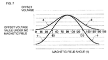
- the relationship between the magnetic field of ⁇ and mid-point potential is represented by a curve c illustrated in Fig. 7 .
- the angle of the magnetic field exceeding the offset voltage value under no magnetic field is limited to a range from 45° to 135°. In other words, no signal is output from the waveform shaping processor outside this angel range and nothing is detected.
- a magnetic sensor includes a bridge circuit in which a serial connection body of a first MR element and a second MR element and a serial connection body of a third MR element and a fourth MR element are connected in parallel between power supplies, and a comparator that receives potential between a node between the first MR element and the second MR element and a node between the third MR element and the fourth MR element to have an output corresponding to a potential difference between both the nodes.
- each of the first and fourth MR elements in the bridge circuit multiple strips along a direction substantially orthogonal to a magnetic-field detection direction are arranged in parallel at certain intervals and are sequentially connected so as to be folded back to form a zigzag pattern in which the multiple strips are electrically connected in series to each other.
- each of the second and third MR elements in the bridge circuit multiple strips, on the whole, along the direction substantially orthogonal to the magnetic-field detection direction are arranged in parallel at certain intervals and are sequentially connected so as to be folded back and, in each of the multiple strips, multiple strips along the magnetic-field detection direction are arranged in parallel at certain intervals and are sequentially connected so as to be folded back to form a zigzag pattern in which the multiple strips are electrically connected in series to each other.
- a bridge circuit in which a serial connection body of a first MR element and a second MR element and a serial connection body of a third MR element and a fourth MR element are connected in parallel between power supplies.
- first and fourth MR elements multiple strips along a direction substantially orthogonal to a magnetic-field detection direction are arranged in parallel at certain intervals and are sequentially connected so as to be folded back to form a zigzag pattern in which the multiple strips are electrically connected in series to each other.
- each of the second and third MR elements multiple strips, on the whole, along the direction substantially orthogonal to the magnetic-field detection direction are arranged in parallel at certain intervals and are sequentially connected so as to be folded back and, in each of the multiple strips, multiple strips along the magnetic-field detection direction are arranged in parallel at certain intervals and are sequentially connected so as to be folded back to form a zigzag pattern in which the multiple strips are electrically connected in series to each other.
- the relationship between the magnetic field of ⁇ and the mid-point potential is represented by a curve d illustrated in Fig. 7 .
- the angle of the magnetic field exceeding the offset voltage value under no magnetic field is greatly increased, compared with the case in (Formula 1).
- the MR elements R2 and R3 in the bridge circuit may be replaced with common semiconductor resistors.
- the resistance values of the resistors made of semiconductor are varied from about ⁇ 10% to about 20%. Consequently, the relative precision with the MR elements is degraded and the balance of the mid-point potential is not capable of being controlled. Thus, the replacement of the MR elements R2 and R3 with the common semiconductor resistors is not practical.
- the R2 and R3 in the bridge circuit which are formed of the MR elements, are formed into a shape that is less affected by the magnetic field to increase the detection angle range.
- Fig. 1A is a plan view for describing the bridge circuit in the magnetic sensor according to the first embodiment of the present invention.
- Fig. 1B is a partially enlarged view for describing the shape of the bridge circuit in detail.
- the magnetic sensor according to the present embodiment includes a bridge circuit in which a serial connection body of an MR element R1 and an MR element R2 and a serial connection body of an MR element R3 and an MR element R4 are connected in parallel between power supply voltage Vcc and grounding GND, a comparator (not illustrated) which receives the potential between a node a between the MR element R1 and the MR element R2 and a node b between the MR element R3 and the MR element R4 to have an output corresponding to corresponding to the potential difference between both the nodes, and a feedback resistor (not illustrated) which feeds back the output from the comparator to one input, as illustrated in Fig. 1A .
- Such circuit elements are formed in the same chip to compose the magnetic sensor.
- the magnetic sensor is featured in the pattern of the MR elements R1 to R4 composing the bridge circuit.
- the MR elements R1 to R4 composing the bridge circuit.
- the MR element R1 and the MR element R4 in the bridge circuit multiple strips along a direction substantially orthogonal to a magnetic-field detection direction are arranged in parallel at certain intervals and are sequentially connected so as to be folded back to form a zigzag pattern in which the multiple strips are electrically connected in series to each other.
- Fig. 1A in each of the MR element R1 and the MR element R4 in the bridge circuit, multiple strips along a direction substantially orthogonal to a magnetic-field detection direction are arranged in parallel at certain intervals and are sequentially connected so as to be folded back to form a zigzag pattern in which the multiple strips are electrically connected in series to each other.
- each of the MR element R2 and the MR element R3 in the bridge circuit multiple strips, on the whole, along the direction substantially orthogonal to the magnetic-field detection direction are arranged in parallel at certain intervals and are sequentially connected so as to be folded back and, in each of the multiple strips, multiple strips along the magnetic-field detection direction are arranged in parallel at certain intervals and are sequentially connected so as to be folded back to form a zigzag pattern in which the multiple strips are electrically connected in series to each other.
- the portions that are folded back to be connected are formed into a substantially linear U shape.
- the MR elements R2 and R3 are composed of the shortest possible straight lines, and straight lines of the same length, like an element e and an element f in Fig. 1A , are arranged so as to be orthogonal to each other to compose the MR elements R2 and R3.
- the length of the straight lines in a first direction in Fig. 1A is made equal to the length of the straight lines in a second direction orthogonal to the first direction.
- the length of the straight lines in the first direction is made equal to the length of the straight lines in the second direction.
- Fig. 2 illustrates the relationship between the line length of the MR element and the rate of change of resistance.
- a case in which the MR element is made of Ni 0.85 Fe 0.15 is illustrated in Fig. 2 .
- the change of resistance of the MR element is reduced to 1/5 or less, compared with lines of 80 ⁇ m or longer, as illustrated in Fig. 5 .
- Arranging the MR elements having the same shape so as to be orthogonal to each other as the R2 and R3 produces a resistance value R represented by (Formula 3) when the magnetic field of ⁇ is applied:
- the MR elements R2 and R3 have significantly small resistance change due to the magnetic field and do not depend on the direction of the magnetic field. Consequently, the offset voltage is equal to (Formula 2).
- the relationship between the magnetic field of ⁇ and the mid-point potential is represented by the curve d illustrated in Fig. 7 . Accordingly, the MR sensor having a large rotation detection angle is provided.
- the magnetic-field detection angle range is increased.
- the magnetic sensor composed of the MR elements in Fig. 6 does not operate because all the resistances of the MR elements R1 to R4 are varied in the same manner.
- the magnetic sensor composed of the MR elements in Fig. 1A is capable of operating.
- Fig. 3 is a plan view for describing the bridge circuit in the magnetic sensor according to the second embodiment of the present invention. A detailed description of the content common to the first embodiment is omitted herein.
- the magnetic sensor of the present embodiment differs from the first embodiment in the pattern shape of the MR elements R1 to R4 composing the bridge circuit. Specifically, as illustrated in Fig. 3 , in each of the MR element R1 and the MR element R4 in the bridge circuit, multiple strips along a direction substantially orthogonal to the magnetic-field detection direction are arranged in parallel at certain intervals and are sequentially connected so as to be folded back to form a zigzag pattern in which the multiple strips are electrically connected in series to each other. In addition, as illustrated in Fig.
- the multiple strips are sequentially connected so as to be folded back in a pattern including multiple 180-degree R shapes to form the zigzag pattern in which the multiple strips are electrically connected in series to each other.
- the portions that are folded back to be connected are formed into a substantially non-linear U shape.
- the MR element R2 and the MR element R3 having the shape and the pattern in the present embodiment are used, the MR element R2 and the MR element R3 do not depend on the direction of the magnetic field and the magnetic-field detection angle range is increased, as in the magnetic sensor of the first embodiment.
- the present invention is not limited to the above embodiments.
- the arrangement of the pattern of the MR elements in the bridge circuit is not limited to the first embodiment illustrated in Fig. 1A and Fig. 1B and to the second embodiment illustrated in Fig. 3 .
- patterns of the MR elements in the bridge circuit illustrated in Fig. 4A and Fig. 4B may be adopted.
- Fig. 4A is a modification of Fig. 1A and Fig. 1B .
- the MR elements R1 and R4 multiple strips, on the whole, along the direction substantially orthogonal to the magnetic-field detection direction are arranged in parallel at certain intervals and are sequentially connected so as to be folded back and, in each of the multiple strips, multiple strips along the magnetic-field detection direction are arranged in parallel at certain intervals and are sequentially connected so as to be folded back to form a zigzag pattern in which the multiple strips are electrically connected in series to each other.
- Fig. 4B is a modification of Fig. 3 .
- the multiple strips are sequentially connected so as to be folded back in the pattern including the multiple 180-degree R shapes to form the zigzag pattern in which the multiple strips are electrically connected in series to each other.
- the MR elements R1 and R4 have significantly small resistance change due to the magnetic field and do not depend on the direction of the magnetic field. Accordingly, the MR sensor having a large rotation detection angle is provided.
- the comparator and the feedback resistor are formed in the same chip as that of the bridge circuit in the first embodiment, the comparator and the feedback resistor may be formed in a different chip.
Landscapes
- Physics & Mathematics (AREA)
- Condensed Matter Physics & Semiconductors (AREA)
- General Physics & Mathematics (AREA)
- Measuring Magnetic Variables (AREA)
- Transmission And Conversion Of Sensor Element Output (AREA)
- Hall/Mr Elements (AREA)
Abstract
Description
- The present invention relates to a bridge circuit and a magnetic sensor including the bridge circuit. More particularly, the present invention relates to a bridge circuit formed of four MR elements and a magnetic sensor including the bridge circuit.
- Magnetic sensors using magneto-resistance effect elements (MR elements) utilizing magneto-resistance effect (MR effect) are known.
Fig. 5 is an equivalent circuit diagram of such a magnetic sensor. Specifically, the magnetic sensor includes a bridge circuit formed of four MR elements R1 to R4, a comparator that receives the potential between a node between the MR element R1 and the MR element R2 and a node between the MR element R3 and the MR element R4 to output the voltage corresponding to the potential difference, and a feedback resistor that feeds back the output from the comparator to one input. Such circuit elements are formed in the same chip to compose the magnetic sensor. -
Fig. 6 is a plan view illustrating a pattern of the MR elements R1 to R4 in such a bridge circuit. Specifically, a serial connection body of the MR element R1 and the MR element R2 and a serial connection body of the MR element R3 and the MR element R4 are connected in parallel between power supply voltage Vcc and grounding GND. In each of the MR element R1 and the MR element R4 in the bridge circuit, multiple strips along a direction orthogonal to a magnetic-field detection direction are arranged in parallel at certain intervals and are sequentially connected so as to be folded back to form a zigzag pattern in which the multiple strips are electrically connected in series to each other. In each of the MR element R2 and the MR element R3 in the bridge circuit, multiple strips along the magnetic-field detection direction are arranged in parallel at certain intervals and are sequentially connected so as to be folded back to form a zigzag pattern in which the multiple strips are electrically connected in series to each other. Such a bridge circuit using the MR elements arranged in the zigzag patterns is proposed inPatent Document 1. - In detection of the position of a rotation operation, there are cases in which an operation angle range of the magnetic sensor is desirably increased as much as possible depending on applications. For example, liquid crystal screen portions of video cameras have rotation mechanisms and the orientations of images on the liquid crystal portions are inverted at angles that are set. At small detection angles, only slight rotation operations may invert the images on the liquid crystal portions. In order to increase the detection angle a little bit, it is necessary to increase magnets in size or devise the arrangement of the magnetic sensors. The degree of freedom of design is reduced with the decrease in size of terminals in recent years and it is desirable to provide the magnetic sensors having large detection angle ranges.
- Patent Document 1: Japanese Unexamined Patent Application Publication No.
2007-225421 - However, the magnetic sensors in the background art described above have the following problems.
- Connecting the four MR elements R1 to R4 differing in at least one resistor body at the four nodes in a bridge pattern and applying power to opposing nodes cause offset voltage at the remaining opposing nodes. Specifically, connecting the serial connection body of the MR element R1 and the MR element R2 and the serial connection body of the MR element R3 and the MR element R4 in parallel between the power supply voltage Vcc and the grounding GND, as illustrated in
Fig. 6 , causes the offset voltage between a node a between the MR element R1 and the MR element R2 and a node b between the MR element R3 and the MR element R4. Upon application of the magnetic field, the MR elements output voltage. The detection level of a waveform shaping processor is set so as to be higher than the level based on the offset voltage from the MR elements. When the level based on the offset voltage from the MR elements exceeds the above detection level, the waveform shaping processor outputs a signal. - Upon application of magnetic field of ∠θ to the pattern illustrated in
Fig. 6 , relationship R=R0-ΔR × sin2θ is established between an angle θ between the current flowing through the MR elements and the magnetic field and the resistance value of the MR elements. In this equation, R0: the resistance value of the MR elements under no magnetic field and ΔR: the amount of change of resistance upon application of the magnetic field. - The offset voltage between the nodes a and b when voltage V is applied is represented by (Formula 1):

The relationship between the magnetic field of ∠θ and mid-point potential is represented by a curve c illustrated inFig. 7 . The angle of the magnetic field exceeding the offset voltage value under no magnetic field is limited to a range from 45° to 135°. In other words, no signal is output from the waveform shaping processor outside this angel range and nothing is detected. - Accordingly, it is an object of the present invention to provide a magnetic sensor having a large magnetic-field detection angle range and a bridge circuit used in the magnetic sensor.
- In order to achieve the above object, a magnetic sensor according to the present invention includes a bridge circuit in which a serial connection body of a first MR element and a second MR element and a serial connection body of a third MR element and a fourth MR element are connected in parallel between power supplies, and a comparator that receives potential between a node between the first MR element and the second MR element and a node between the third MR element and the fourth MR element to have an output corresponding to a potential difference between both the nodes. In each of the first and fourth MR elements in the bridge circuit, multiple strips along a direction substantially orthogonal to a magnetic-field detection direction are arranged in parallel at certain intervals and are sequentially connected so as to be folded back to form a zigzag pattern in which the multiple strips are electrically connected in series to each other. In each of the second and third MR elements in the bridge circuit, multiple strips, on the whole, along the direction substantially orthogonal to the magnetic-field detection direction are arranged in parallel at certain intervals and are sequentially connected so as to be folded back and, in each of the multiple strips, multiple strips along the magnetic-field detection direction are arranged in parallel at certain intervals and are sequentially connected so as to be folded back to form a zigzag pattern in which the multiple strips are electrically connected in series to each other.
- A bridge circuit according to the present invention is provided in which a serial connection body of a first MR element and a second MR element and a serial connection body of a third MR element and a fourth MR element are connected in parallel between power supplies. In each of the first and fourth MR elements, multiple strips along a direction substantially orthogonal to a magnetic-field detection direction are arranged in parallel at certain intervals and are sequentially connected so as to be folded back to form a zigzag pattern in which the multiple strips are electrically connected in series to each other. In each of the second and third MR elements, multiple strips, on the whole, along the direction substantially orthogonal to the magnetic-field detection direction are arranged in parallel at certain intervals and are sequentially connected so as to be folded back and, in each of the multiple strips, multiple strips along the magnetic-field detection direction are arranged in parallel at certain intervals and are sequentially connected so as to be folded back to form a zigzag pattern in which the multiple strips are electrically connected in series to each other.
- According to the present invention, it is possible to increase the magnetic-field detection angle range.
-
- [
Fig. 1A] Fig. 1A is a plan view for describing a bridge circuit in a magnetic sensor according to a first embodiment of the present invention. - [
Fig. 1B] Fig. 1B is a partially enlarged view for describing the shape of the bridge circuit in the magnetic sensor according to the first embodiment of the present invention in detail. - [
Fig. 2] Fig. 2 is a graph illustrating the relationship between the line length of an MR element and the rate of change of resistance. - [
Fig. 3] Fig. 3 is a plan view for describing a bridge circuit in a magnetic sensor according to a second embodiment of the present invention. - [
Fig. 4A] Fig. 4A is a plan view for describing a bridge circuit in a magnetic sensor according to another embodiment of the present invention. - [
Fig. 4B] Fig. 4B is a plan view for describing a bridge circuit in a magnetic sensor according to another embodiment of the present invention. - [
Fig. 5] Fig. 5 is an equivalent circuit diagram of a magnetic sensor. - [
Fig. 6] Fig. 6 is a plan view illustrating an exemplary MR pattern in a bridge circuit in a magnetic sensor. - [
Fig. 7] Fig. 7 is a graph illustrating the relationship between magnetic field of ∠θ and mid-point potential. - Before detailed description of preferred embodiments of the present invention, the offset voltage of the magnetic sensor will now be described again. If the MR elements R2 and R3 illustrated in
Fig. 6 are replaced with resistor bodies that are not affected by the magnetic field, the offset voltage between the nodes a and b is represented by (Formula 2):
In this case, the relationship between the magnetic field of ∠θ and the mid-point potential is represented by a curve d illustrated inFig. 7 . The angle of the magnetic field exceeding the offset voltage value under no magnetic field is greatly increased, compared with the case in (Formula 1). - As described above, replacing the MR elements R2 and R3 in the bridge circuit with the resistor bodies that do not depend on the magnetic field allows the detection angle of the magnetic sensor to be increased. Accordingly, the MR elements R2 and R3 may be replaced with common semiconductor resistors. However, in consideration of practical mass production, the resistance values of the resistors made of semiconductor are varied from about ±10% to about 20%. Consequently, the relative precision with the MR elements is degraded and the balance of the mid-point potential is not capable of being controlled. Thus, the replacement of the MR elements R2 and R3 with the common semiconductor resistors is not practical.
- Accordingly, in the present invention, the R2 and R3 in the bridge circuit, which are formed of the MR elements, are formed into a shape that is less affected by the magnetic field to increase the detection angle range.
- First, a bridge circuit according to a first embodiment of the present invention and a magnetic sensor including the bridge circuit will now be described with reference to the drawings.
Fig. 1A is a plan view for describing the bridge circuit in the magnetic sensor according to the first embodiment of the present invention.Fig. 1B is a partially enlarged view for describing the shape of the bridge circuit in detail. - The magnetic sensor according to the present embodiment includes a bridge circuit in which a serial connection body of an MR element R1 and an MR element R2 and a serial connection body of an MR element R3 and an MR element R4 are connected in parallel between power supply voltage Vcc and grounding GND, a comparator (not illustrated) which receives the potential between a node a between the MR element R1 and the MR element R2 and a node b between the MR element R3 and the MR element R4 to have an output corresponding to corresponding to the potential difference between both the nodes, and a feedback resistor (not illustrated) which feeds back the output from the comparator to one input, as illustrated in
Fig. 1A . Such circuit elements are formed in the same chip to compose the magnetic sensor. - In addition, the magnetic sensor is featured in the pattern of the MR elements R1 to R4 composing the bridge circuit. Specifically, as illustrated in
Fig. 1A , in each of the MR element R1 and the MR element R4 in the bridge circuit, multiple strips along a direction substantially orthogonal to a magnetic-field detection direction are arranged in parallel at certain intervals and are sequentially connected so as to be folded back to form a zigzag pattern in which the multiple strips are electrically connected in series to each other. In addition, as illustrated inFig. 1A , in each of the MR element R2 and the MR element R3 in the bridge circuit, multiple strips, on the whole, along the direction substantially orthogonal to the magnetic-field detection direction are arranged in parallel at certain intervals and are sequentially connected so as to be folded back and, in each of the multiple strips, multiple strips along the magnetic-field detection direction are arranged in parallel at certain intervals and are sequentially connected so as to be folded back to form a zigzag pattern in which the multiple strips are electrically connected in series to each other. The portions that are folded back to be connected are formed into a substantially linear U shape. - More specifically, as illustrated in
Fig. 1A , the MR elements R2 and R3 are composed of the shortest possible straight lines, and straight lines of the same length, like an element e and an element f inFig. 1A , are arranged so as to be orthogonal to each other to compose the MR elements R2 and R3. In other words, as for the MR element R2, the length of the straight lines in a first direction inFig. 1A is made equal to the length of the straight lines in a second direction orthogonal to the first direction. Also as for the MR element R3, the length of the straight lines in the first direction is made equal to the length of the straight lines in the second direction. - Since each of the MR elements R2 and R3 is composed of the short lines, the resistance change of the MR elements, which are anisotropic magneto-resistance elements, relative to the magnetic field is greatly smaller than that of the MR elements R1 and R4.
Fig. 2 illustrates the relationship between the line length of the MR element and the rate of change of resistance. A case in which the MR element is made of Ni0.85Fe0.15 is illustrated inFig. 2 . For example, when a length h resulting from exclusion of an area overlapped with the orthogonal pattern from a line g inFig. 1B is shorter than or equal to 10 µm, the change of resistance of the MR element is reduced to 1/5 or less, compared with lines of 80 µm or longer, as illustrated inFig. 5 . - Arranging the MR elements having the same shape so as to be orthogonal to each other as the R2 and R3 produces a resistance value R represented by (Formula 3) when the magnetic field of ∠θ is applied:

Accordingly, the resistance value R does not theoretically depend on the angle of the applied magnetic field. - As described above, when the bridge circuit in
Fig. 5 composed of the MR elements inFig. 1A is considered, the MR elements R2 and R3 have significantly small resistance change due to the magnetic field and do not depend on the direction of the magnetic field. Consequently, the offset voltage is equal to (Formula 2). The relationship between the magnetic field of ∠θ and the mid-point potential is represented by the curve d illustrated inFig. 7 . Accordingly, the MR sensor having a large rotation detection angle is provided. - According to the magnetic sensor of the present embodiment, the magnetic-field detection angle range is increased. For example, when magnetic field of θ=45° is applied, the magnetic sensor composed of the MR elements in
Fig. 6 does not operate because all the resistances of the MR elements R1 to R4 are varied in the same manner. In contrast, the magnetic sensor composed of the MR elements inFig. 1A is capable of operating. - Next, a bridge circuit according to a second embodiment of the present invention and a magnetic sensor including the bridge circuit will now be described with reference to the drawing.
Fig. 3 is a plan view for describing the bridge circuit in the magnetic sensor according to the second embodiment of the present invention. A detailed description of the content common to the first embodiment is omitted herein. - The magnetic sensor of the present embodiment differs from the first embodiment in the pattern shape of the MR elements R1 to R4 composing the bridge circuit. Specifically, as illustrated in
Fig. 3 , in each of the MR element R1 and the MR element R4 in the bridge circuit, multiple strips along a direction substantially orthogonal to the magnetic-field detection direction are arranged in parallel at certain intervals and are sequentially connected so as to be folded back to form a zigzag pattern in which the multiple strips are electrically connected in series to each other. In addition, as illustrated inFig. 3 , in each of the MR element R2 and the MR element R3 in the bridge circuit, multiple strips, on the whole, along the direction substantially orthogonal to the magnetic-field detection direction are arranged in parallel at certain intervals and are sequentially connected so as to be folded back and, in each of the multiple strips, multiple strips along the magnetic-field detection direction are arranged in parallel at certain intervals and are sequentially connected so as to be folded back to form a zigzag pattern in which the multiple strips are electrically connected in series to each other. - As illustrated in
Fig. 3 , in the present embodiment, in the MR elements R2 and the MR element R3 in the bridge circuit, the multiple strips are sequentially connected so as to be folded back in a pattern including multiple 180-degree R shapes to form the zigzag pattern in which the multiple strips are electrically connected in series to each other. In other words, the portions that are folded back to be connected are formed into a substantially non-linear U shape. - Also when the MR element R2 and the MR element R3 having the shape and the pattern in the present embodiment are used, the MR element R2 and the MR element R3 do not depend on the direction of the magnetic field and the magnetic-field detection angle range is increased, as in the magnetic sensor of the first embodiment.
- Although the preferred embodiments of the present invention are described above, the present invention is not limited to the above embodiments. The arrangement of the pattern of the MR elements in the bridge circuit is not limited to the first embodiment illustrated in
Fig. 1A and Fig. 1B and to the second embodiment illustrated inFig. 3 . For example, patterns of the MR elements in the bridge circuit illustrated inFig. 4A and Fig. 4B may be adopted. -
Fig. 4A is a modification ofFig. 1A and Fig. 1B . In each of the MR elements R1 and R4, multiple strips, on the whole, along the direction substantially orthogonal to the magnetic-field detection direction are arranged in parallel at certain intervals and are sequentially connected so as to be folded back and, in each of the multiple strips, multiple strips along the magnetic-field detection direction are arranged in parallel at certain intervals and are sequentially connected so as to be folded back to form a zigzag pattern in which the multiple strips are electrically connected in series to each other. -
Fig. 4B is a modification ofFig. 3 . In each of the MR elements R1 and R4, multiple strips, on the whole, along the direction substantially orthogonal to the magnetic-field detection direction are arranged in parallel at certain intervals and are sequentially connected so as to be folded back and, in each of the multiple strips, multiple strips along the magnetic-field detection direction are arranged in parallel at certain intervals and are sequentially connected so as to be folded back to form a zigzag pattern in which the multiple strips are electrically connected in series to each other. As in the case inFig. 3 , the multiple strips are sequentially connected so as to be folded back in the pattern including the multiple 180-degree R shapes to form the zigzag pattern in which the multiple strips are electrically connected in series to each other. - In these cases, the MR elements R1 and R4 have significantly small resistance change due to the magnetic field and do not depend on the direction of the magnetic field. Accordingly, the MR sensor having a large rotation detection angle is provided.
- Although the comparator and the feedback resistor are formed in the same chip as that of the bridge circuit in the first embodiment, the comparator and the feedback resistor may be formed in a different chip.
- Although the invention of the present application is described above with reference to the preferred embodiments, the invention of the present application is not limited to the above embodiments. Various changes and modified embodiments of the configuration and the detailed portions of the invention of the present application will be obvious to those skilled in the art without departing from the scope of the invention of the present application.
- This application is based upon and claims the benefit of priority of the prior Japanese Patent Application No.
2012-112497, filed on May 16, 2012 - Electronic devices and industrial equipment requiring the position detection are considered as exemplary applications of the present invention.
-
- R1, R2, R3, R4 MR element
- a, b node
- g line
Claims (9)
- A magnetic sensor comprising:a bridge circuit in which a serial connection body of a first MR element and a second MR element and a serial connection body of a third MR element and a fourth MR element are connected in parallel between power supplies, and a comparator that receives potential between a node between the first MR element and the second MR element and a node between the third MR element and the fourth MR element to have an output corresponding to a potential difference between both the nodes,wherein, in each of the first and fourth MR elements in the bridge circuit, multiple strips along a direction substantially orthogonal to a magnetic-field detection direction are arranged in parallel at certain intervals and are sequentially connected so as to be folded back to form a zigzag pattern in which the multiple strips are electrically connected in series to each other, andwherein, in each of the second and third MR elements in the bridge circuit, multiple strips, on the whole, along the direction substantially orthogonal to the magnetic-field detection direction are arranged in parallel at certain intervals and are sequentially connected so as to be folded back and, in each of the multiple strips, multiple strips along the magnetic-field detection direction are arranged in parallel at certain intervals and are sequentially connected so as to be folded back to form a zigzag pattern in which the multiple strips are electrically connected in series to each other.
- The magnetic sensor according to Claim 1,
wherein the multiple strips in the second and third MR elements are shorter than the multiple strips in the first and fourth MR elements. - The magnetic sensor according to Claim 1 or 2,
wherein each of the second and third MR elements is composed of multiple straight lines and a straight-line distance resulting from exclusion of an area where the straight lines intersect with each other is shorter than or equal to 10 µm. - The magnetic sensor according to any of Claims 1 to 3,
wherein, in each of the second and third MR elements, the multiple strips are sequentially connected so as to be folded back in a pattern including multiple 180-degree R shapes. - The magnetic sensor according to any of Claims 1 to 3,
wherein, in each of the first and fourth MR elements, the portions that are folded back to be connected are formed into a substantially linear U shape. - The magnetic sensor according to any of Claims 1 to 3,
wherein, in each of the first and fourth MR elements, the portions that are folded back to be connected are formed into a substantially non-linear U shape. - A bridge circuit in which a serial connection body of a first MR element and a second MR element and a serial connection body of a third MR element and a fourth MR element are connected in parallel between power supplies,
wherein, in each of the first and fourth MR elements, multiple strips along a direction substantially orthogonal to a magnetic-field detection direction are arranged in parallel at certain intervals and are sequentially connected so as to be folded back to form a zigzag pattern in which the multiple strips are electrically connected in series to each other, and
wherein, in each of the second and third MR elements, multiple strips, on the whole, along the direction substantially orthogonal to the magnetic-field detection direction are arranged in parallel at certain intervals and are sequentially connected so as to be folded back and, in each of the multiple strips, multiple strips along the magnetic-field detection direction are arranged in parallel at certain intervals and are sequentially connected so as to be folded back to form a zigzag pattern in which the multiple strips are electrically connected in series to each other. - The bridge circuit according to Claim 7,
wherein the multiple strips in the second and third MR elements are shorter than the multiple strips in the first and fourth MR elements. - The bridge circuit according to Claim 7 or 8,
wherein each of the second and third MR elements is composed of multiple straight lines and a straight-line distance resulting from exclusion of an area where the straight lines intersect with each other is shorter than or equal to 10 µm.
Applications Claiming Priority (2)
| Application Number | Priority Date | Filing Date | Title |
|---|---|---|---|
| JP2012112497 | 2012-05-16 | ||
| PCT/JP2013/002703 WO2013171977A1 (en) | 2012-05-16 | 2013-04-22 | Bridge circuit and magnetic sensor comprising same |
Publications (2)
| Publication Number | Publication Date |
|---|---|
| EP2853909A1 true EP2853909A1 (en) | 2015-04-01 |
| EP2853909A4 EP2853909A4 (en) | 2016-01-20 |
Family
ID=49583410
Family Applications (1)
| Application Number | Title | Priority Date | Filing Date |
|---|---|---|---|
| EP13790381.1A Withdrawn EP2853909A4 (en) | 2012-05-16 | 2013-04-22 | Bridge circuit and magnetic sensor comprising same |
Country Status (5)
| Country | Link |
|---|---|
| US (1) | US20150115949A1 (en) |
| EP (1) | EP2853909A4 (en) |
| JP (1) | JPWO2013171977A1 (en) |
| CN (1) | CN104272129A (en) |
| WO (1) | WO2013171977A1 (en) |
Families Citing this family (7)
| Publication number | Priority date | Publication date | Assignee | Title |
|---|---|---|---|---|
| CN105223523B (en) * | 2014-05-30 | 2018-04-27 | 株式会社村田制作所 | Magnetic sensor |
| WO2016013346A1 (en) * | 2014-07-23 | 2016-01-28 | 株式会社村田製作所 | Magnetic sensor |
| JP6369548B2 (en) | 2014-07-24 | 2018-08-08 | 株式会社村田製作所 | Magnetic sensor |
| JP6296160B2 (en) | 2014-07-25 | 2018-03-20 | 株式会社村田製作所 | Magnetic sensor |
| CN105093139B (en) * | 2015-06-09 | 2017-11-24 | 江苏多维科技有限公司 | A kind of push-pull type X-axis magnetic resistance sensor |
| CN109752677A (en) * | 2019-01-10 | 2019-05-14 | 东南大学 | A double bridge type thin film magnetoresistive sensor |
| TWI705262B (en) * | 2019-09-27 | 2020-09-21 | 愛盛科技股份有限公司 | Magnetic field sensing apparatus |
Family Cites Families (22)
| Publication number | Priority date | Publication date | Assignee | Title |
|---|---|---|---|---|
| JPS6422076A (en) * | 1987-07-17 | 1989-01-25 | Fujitsu Ltd | Magnetoresistance element |
| JPH02231587A (en) * | 1989-03-03 | 1990-09-13 | Tokai Rika Co Ltd | Reference voltage generating device |
| JPH04133221A (en) * | 1990-09-26 | 1992-05-07 | Nec Corp | Magnetic sensor |
| JP2551321B2 (en) * | 1993-04-21 | 1996-11-06 | 日本電気株式会社 | Integrated magnetoresistive sensor |
| JP2655106B2 (en) * | 1994-12-07 | 1997-09-17 | 日本電気株式会社 | Magnetoresistive sensor |
| JPH09127221A (en) * | 1995-10-27 | 1997-05-16 | Sony Corp | Geomagnetic direction sensor |
| JP3404249B2 (en) * | 1997-03-26 | 2003-05-06 | 三菱電機株式会社 | Magnetic sensor |
| JP3587678B2 (en) * | 1998-03-20 | 2004-11-10 | Tdk株式会社 | Magnetic field sensor |
| DE10308030B4 (en) * | 2003-02-24 | 2011-02-03 | Meas Deutschland Gmbh | Magnetoresistive sensor for determining an angle or position |
| JP4259937B2 (en) * | 2003-06-30 | 2009-04-30 | アルプス電気株式会社 | Angle detection sensor |
| JP4977378B2 (en) * | 2006-02-23 | 2012-07-18 | 山梨日本電気株式会社 | Magnetic sensor, rotation detection device, and position detection device |
| JP2008046076A (en) * | 2006-08-21 | 2008-02-28 | Alps Electric Co Ltd | Method of manufacturing magnetic sensor, and magnetic sensor |
| JP4406632B2 (en) * | 2006-08-31 | 2010-02-03 | アルプス電気株式会社 | Magnetic detection device and manufacturing method thereof |
| CN101512368B (en) * | 2006-08-31 | 2012-07-25 | 阿尔卑斯电气株式会社 | Magnetic detection device |
| JP2008209224A (en) * | 2007-02-26 | 2008-09-11 | Daido Steel Co Ltd | Magnetic sensor |
| WO2009031539A1 (en) * | 2007-09-03 | 2009-03-12 | Alps Electric Co., Ltd. | Magnetic detecting device |
| EP2416125B1 (en) * | 2009-03-30 | 2015-01-07 | Hitachi Metals, Ltd. | Rotation angle detection device |
| US8451003B2 (en) * | 2009-07-29 | 2013-05-28 | Tdk Corporation | Magnetic sensor having magneto-resistive elements on a substrate |
| US8564286B2 (en) * | 2010-06-28 | 2013-10-22 | Infineon Technologies Ag | GMR sensors having reduced AMR effects |
| CN201935997U (en) * | 2010-08-11 | 2011-08-17 | 上海腾怡半导体有限公司 | Magnetic field sensor chip |
| JP2013016630A (en) * | 2011-07-04 | 2013-01-24 | Yamanashi Nippon Denki Kk | Magnetoresistance effect element and magnetic sensor using the same |
| US9310446B2 (en) * | 2012-10-18 | 2016-04-12 | Analog Devices, Inc. | Magnetic field direction detector |
-
2013
- 2013-04-22 JP JP2014515479A patent/JPWO2013171977A1/en active Pending
- 2013-04-22 CN CN201380022667.5A patent/CN104272129A/en active Pending
- 2013-04-22 WO PCT/JP2013/002703 patent/WO2013171977A1/en not_active Ceased
- 2013-04-22 EP EP13790381.1A patent/EP2853909A4/en not_active Withdrawn
-
2014
- 2014-10-30 US US14/527,846 patent/US20150115949A1/en not_active Abandoned
Also Published As
| Publication number | Publication date |
|---|---|
| US20150115949A1 (en) | 2015-04-30 |
| CN104272129A (en) | 2015-01-07 |
| JPWO2013171977A1 (en) | 2016-01-12 |
| WO2013171977A1 (en) | 2013-11-21 |
| EP2853909A4 (en) | 2016-01-20 |
Similar Documents
| Publication | Publication Date | Title |
|---|---|---|
| EP2853909A1 (en) | Bridge circuit and magnetic sensor comprising same | |
| EP2769231B1 (en) | Dual-axis anisotropic magnetoresistive sensors | |
| US8193805B2 (en) | Magnetic sensor | |
| CN103376426B (en) | Magnetic field sensor | |
| US9297635B2 (en) | Magnetic sensor system including two detection circuits | |
| EP2284495A2 (en) | Magnetic sensor | |
| US10302712B2 (en) | Magnetic field sensing apparatus | |
| US11243275B2 (en) | Magnetic field sensing device | |
| US11474168B2 (en) | Magnetic sensor device | |
| US20220326320A1 (en) | Magnetic sensor | |
| CN110007255B (en) | Magnetic field sensing device | |
| US20120306488A1 (en) | Spin-valve magnetoresistance structure and spin-valve magnetoresistance sensor | |
| JP2017072375A (en) | Magnetic sensor | |
| CN110857952A (en) | current sensor | |
| JP2016145745A (en) | Magnetic sensor | |
| US10295615B2 (en) | Magnetic sensor | |
| JP2016115240A (en) | Multiplication circuit and power sensor including the same | |
| WO2016111278A1 (en) | Current sensor | |
| JP2016142652A (en) | Power sensor | |
| US9869730B2 (en) | Magnetic detection apparatus | |
| TWI714107B (en) | Electric current sensor | |
| TWI703338B (en) | Electric current sensor | |
| CN110857951B (en) | current sensor | |
| CN112578322A (en) | Magnetic field sensing device | |
| JP2008527370A (en) | Angle sensor |
Legal Events
| Date | Code | Title | Description |
|---|---|---|---|
| PUAI | Public reference made under article 153(3) epc to a published international application that has entered the european phase |
Free format text: ORIGINAL CODE: 0009012 |
|
| 17P | Request for examination filed |
Effective date: 20141003 |
|
| AK | Designated contracting states |
Kind code of ref document: A1 Designated state(s): AL AT BE BG CH CY CZ DE DK EE ES FI FR GB GR HR HU IE IS IT LI LT LU LV MC MK MT NL NO PL PT RO RS SE SI SK SM TR |
|
| AX | Request for extension of the european patent |
Extension state: BA ME |
|
| DAX | Request for extension of the european patent (deleted) | ||
| RA4 | Supplementary search report drawn up and despatched (corrected) |
Effective date: 20151217 |
|
| RIC1 | Information provided on ipc code assigned before grant |
Ipc: H01L 43/08 20060101ALI20151211BHEP Ipc: G01R 33/09 20060101AFI20151211BHEP |
|
| STAA | Information on the status of an ep patent application or granted ep patent |
Free format text: STATUS: THE APPLICATION IS DEEMED TO BE WITHDRAWN |
|
| 18D | Application deemed to be withdrawn |
Effective date: 20160722 |