EP2851968B1 - Light-emitting device - Google Patents
Light-emitting device Download PDFInfo
- Publication number
- EP2851968B1 EP2851968B1 EP13791696.1A EP13791696A EP2851968B1 EP 2851968 B1 EP2851968 B1 EP 2851968B1 EP 13791696 A EP13791696 A EP 13791696A EP 2851968 B1 EP2851968 B1 EP 2851968B1
- Authority
- EP
- European Patent Office
- Prior art keywords
- light
- layer
- region
- reflective electrode
- semiconductor layer
- Prior art date
- Legal status (The legal status is an assumption and is not a legal conclusion. Google has not performed a legal analysis and makes no representation as to the accuracy of the status listed.)
- Active
Links
- 239000004065 semiconductor Substances 0.000 claims description 171
- 229910052751 metal Inorganic materials 0.000 claims description 80
- 239000002184 metal Substances 0.000 claims description 80
- 230000002093 peripheral effect Effects 0.000 claims description 11
- 238000005468 ion implantation Methods 0.000 claims description 5
- 239000000758 substrate Substances 0.000 description 48
- 239000000463 material Substances 0.000 description 36
- XLOMVQKBTHCTTD-UHFFFAOYSA-N Zinc monoxide Chemical compound [Zn]=O XLOMVQKBTHCTTD-UHFFFAOYSA-N 0.000 description 24
- 230000003287 optical effect Effects 0.000 description 21
- 238000000034 method Methods 0.000 description 20
- 239000010949 copper Substances 0.000 description 14
- 229910052802 copper Inorganic materials 0.000 description 13
- PXHVJJICTQNCMI-UHFFFAOYSA-N nickel Substances [Ni] PXHVJJICTQNCMI-UHFFFAOYSA-N 0.000 description 13
- 239000011787 zinc oxide Substances 0.000 description 13
- 239000002019 doping agent Substances 0.000 description 12
- 229910052759 nickel Inorganic materials 0.000 description 11
- 229910052804 chromium Inorganic materials 0.000 description 10
- 229910052719 titanium Inorganic materials 0.000 description 10
- 239000010936 titanium Substances 0.000 description 10
- 229910045601 alloy Inorganic materials 0.000 description 9
- 239000000956 alloy Substances 0.000 description 9
- 229910052782 aluminium Inorganic materials 0.000 description 9
- 238000000605 extraction Methods 0.000 description 9
- -1 acryl Chemical group 0.000 description 8
- 150000001875 compounds Chemical class 0.000 description 8
- JAONJTDQXUSBGG-UHFFFAOYSA-N dialuminum;dizinc;oxygen(2-) Chemical compound [O-2].[O-2].[O-2].[O-2].[O-2].[Al+3].[Al+3].[Zn+2].[Zn+2] JAONJTDQXUSBGG-UHFFFAOYSA-N 0.000 description 8
- 238000009792 diffusion process Methods 0.000 description 8
- 229910052697 platinum Inorganic materials 0.000 description 8
- 239000004417 polycarbonate Substances 0.000 description 8
- 229920000515 polycarbonate Polymers 0.000 description 8
- 230000005855 radiation Effects 0.000 description 8
- 229910052709 silver Inorganic materials 0.000 description 8
- SKRWFPLZQAAQSU-UHFFFAOYSA-N stibanylidynetin;hydrate Chemical compound O.[Sn].[Sb] SKRWFPLZQAAQSU-UHFFFAOYSA-N 0.000 description 8
- 229910052721 tungsten Inorganic materials 0.000 description 8
- 229910052725 zinc Inorganic materials 0.000 description 8
- 239000011701 zinc Substances 0.000 description 8
- 229960001296 zinc oxide Drugs 0.000 description 8
- 230000004888 barrier function Effects 0.000 description 7
- 238000000465 moulding Methods 0.000 description 7
- 229910002704 AlGaN Inorganic materials 0.000 description 6
- 230000008878 coupling Effects 0.000 description 6
- 238000010168 coupling process Methods 0.000 description 6
- 238000005859 coupling reaction Methods 0.000 description 6
- 238000005530 etching Methods 0.000 description 6
- 229910052733 gallium Inorganic materials 0.000 description 6
- 229910052737 gold Inorganic materials 0.000 description 6
- 229910052738 indium Inorganic materials 0.000 description 6
- 238000004020 luminiscence type Methods 0.000 description 6
- 229910052720 vanadium Inorganic materials 0.000 description 6
- 229910001218 Gallium arsenide Inorganic materials 0.000 description 5
- 150000004767 nitrides Chemical class 0.000 description 5
- 229920003023 plastic Polymers 0.000 description 5
- 239000004033 plastic Substances 0.000 description 5
- 229920005989 resin Polymers 0.000 description 5
- 239000011347 resin Substances 0.000 description 5
- 229910052710 silicon Inorganic materials 0.000 description 5
- 229910052718 tin Inorganic materials 0.000 description 5
- 239000012463 white pigment Substances 0.000 description 5
- KEQXNNJHMWSZHK-UHFFFAOYSA-L 1,3,2,4$l^{2}-dioxathiaplumbetane 2,2-dioxide Chemical compound [Pb+2].[O-]S([O-])(=O)=O KEQXNNJHMWSZHK-UHFFFAOYSA-L 0.000 description 4
- GYHNNYVSQQEPJS-UHFFFAOYSA-N Gallium Chemical compound [Ga] GYHNNYVSQQEPJS-UHFFFAOYSA-N 0.000 description 4
- 239000004698 Polyethylene Substances 0.000 description 4
- 239000004743 Polypropylene Substances 0.000 description 4
- DZLPZFLXRVRDAE-UHFFFAOYSA-N [O--].[O--].[O--].[O--].[Al+3].[Zn++].[In+3] Chemical compound [O--].[O--].[O--].[O--].[Al+3].[Zn++].[In+3] DZLPZFLXRVRDAE-UHFFFAOYSA-N 0.000 description 4
- 229910052732 germanium Inorganic materials 0.000 description 4
- 239000012535 impurity Substances 0.000 description 4
- APFVFJFRJDLVQX-UHFFFAOYSA-N indium atom Chemical compound [In] APFVFJFRJDLVQX-UHFFFAOYSA-N 0.000 description 4
- AMGQUBHHOARCQH-UHFFFAOYSA-N indium;oxotin Chemical compound [In].[Sn]=O AMGQUBHHOARCQH-UHFFFAOYSA-N 0.000 description 4
- HRHKULZDDYWVBE-UHFFFAOYSA-N indium;oxozinc;tin Chemical compound [In].[Sn].[Zn]=O HRHKULZDDYWVBE-UHFFFAOYSA-N 0.000 description 4
- 239000011810 insulating material Substances 0.000 description 4
- 239000011777 magnesium Substances 0.000 description 4
- 229910052750 molybdenum Inorganic materials 0.000 description 4
- 229910052763 palladium Inorganic materials 0.000 description 4
- 229920003229 poly(methyl methacrylate) Polymers 0.000 description 4
- 229920000573 polyethylene Polymers 0.000 description 4
- 239000004926 polymethyl methacrylate Substances 0.000 description 4
- 229920001155 polypropylene Polymers 0.000 description 4
- 229910001887 tin oxide Inorganic materials 0.000 description 4
- YVTHLONGBIQYBO-UHFFFAOYSA-N zinc indium(3+) oxygen(2-) Chemical compound [O--].[Zn++].[In+3] YVTHLONGBIQYBO-UHFFFAOYSA-N 0.000 description 4
- 229910002601 GaN Inorganic materials 0.000 description 3
- 239000004020 conductor Substances 0.000 description 3
- 239000012212 insulator Substances 0.000 description 3
- 229910052749 magnesium Inorganic materials 0.000 description 3
- 238000004519 manufacturing process Methods 0.000 description 3
- 239000007769 metal material Substances 0.000 description 3
- 229910003465 moissanite Inorganic materials 0.000 description 3
- 229920000139 polyethylene terephthalate Polymers 0.000 description 3
- 239000005020 polyethylene terephthalate Substances 0.000 description 3
- 229910010271 silicon carbide Inorganic materials 0.000 description 3
- 229910017944 Ag—Cu Inorganic materials 0.000 description 2
- 229910000980 Aluminium gallium arsenide Inorganic materials 0.000 description 2
- 229920000089 Cyclic olefin copolymer Polymers 0.000 description 2
- 239000004713 Cyclic olefin copolymer Substances 0.000 description 2
- 229910005540 GaP Inorganic materials 0.000 description 2
- 229910002668 Pd-Cu Inorganic materials 0.000 description 2
- 229910019897 RuOx Inorganic materials 0.000 description 2
- 229910000577 Silicon-germanium Inorganic materials 0.000 description 2
- BQCADISMDOOEFD-UHFFFAOYSA-N Silver Chemical compound [Ag] BQCADISMDOOEFD-UHFFFAOYSA-N 0.000 description 2
- RNQKDQAVIXDKAG-UHFFFAOYSA-N aluminum gallium Chemical compound [Al].[Ga] RNQKDQAVIXDKAG-UHFFFAOYSA-N 0.000 description 2
- 229910052786 argon Inorganic materials 0.000 description 2
- 229910052788 barium Inorganic materials 0.000 description 2
- 229910052797 bismuth Inorganic materials 0.000 description 2
- 238000000071 blow moulding Methods 0.000 description 2
- 229910052791 calcium Inorganic materials 0.000 description 2
- 239000011575 calcium Substances 0.000 description 2
- 239000012141 concentrate Substances 0.000 description 2
- 230000000694 effects Effects 0.000 description 2
- YZZNJYQZJKSEER-UHFFFAOYSA-N gallium tin Chemical compound [Ga].[Sn] YZZNJYQZJKSEER-UHFFFAOYSA-N 0.000 description 2
- 239000011521 glass Substances 0.000 description 2
- 239000010931 gold Substances 0.000 description 2
- 229910052735 hafnium Inorganic materials 0.000 description 2
- 230000017525 heat dissipation Effects 0.000 description 2
- 238000002513 implantation Methods 0.000 description 2
- 150000002500 ions Chemical class 0.000 description 2
- 229910052741 iridium Inorganic materials 0.000 description 2
- 229910052742 iron Inorganic materials 0.000 description 2
- VRIVJOXICYMTAG-IYEMJOQQSA-L iron(ii) gluconate Chemical compound [Fe+2].OC[C@@H](O)[C@@H](O)[C@H](O)[C@@H](O)C([O-])=O.OC[C@@H](O)[C@@H](O)[C@H](O)[C@@H](O)C([O-])=O VRIVJOXICYMTAG-IYEMJOQQSA-L 0.000 description 2
- 238000002955 isolation Methods 0.000 description 2
- GNRSAWUEBMWBQH-UHFFFAOYSA-N nickel(II) oxide Inorganic materials [Ni]=O GNRSAWUEBMWBQH-UHFFFAOYSA-N 0.000 description 2
- 229910052757 nitrogen Inorganic materials 0.000 description 2
- 229910052760 oxygen Inorganic materials 0.000 description 2
- BASFCYQUMIYNBI-UHFFFAOYSA-N platinum Substances [Pt] BASFCYQUMIYNBI-UHFFFAOYSA-N 0.000 description 2
- 229920003207 poly(ethylene-2,6-naphthalate) Polymers 0.000 description 2
- 239000011112 polyethylene naphthalate Substances 0.000 description 2
- 230000001681 protective effect Effects 0.000 description 2
- 239000002096 quantum dot Substances 0.000 description 2
- 229910052711 selenium Inorganic materials 0.000 description 2
- 239000004332 silver Substances 0.000 description 2
- 229910052712 strontium Inorganic materials 0.000 description 2
- 239000000126 substance Substances 0.000 description 2
- 230000003746 surface roughness Effects 0.000 description 2
- 229910052715 tantalum Inorganic materials 0.000 description 2
- 229910052714 tellurium Inorganic materials 0.000 description 2
- RYGMFSIKBFXOCR-UHFFFAOYSA-N Copper Chemical compound [Cu] RYGMFSIKBFXOCR-UHFFFAOYSA-N 0.000 description 1
- FYYHWMGAXLPEAU-UHFFFAOYSA-N Magnesium Chemical compound [Mg] FYYHWMGAXLPEAU-UHFFFAOYSA-N 0.000 description 1
- BPQQTUXANYXVAA-UHFFFAOYSA-N Orthosilicate Chemical compound [O-][Si]([O-])([O-])[O-] BPQQTUXANYXVAA-UHFFFAOYSA-N 0.000 description 1
- OAICVXFJPJFONN-UHFFFAOYSA-N Phosphorus Chemical compound [P] OAICVXFJPJFONN-UHFFFAOYSA-N 0.000 description 1
- ATJFFYVFTNAWJD-UHFFFAOYSA-N Tin Chemical compound [Sn] ATJFFYVFTNAWJD-UHFFFAOYSA-N 0.000 description 1
- 239000000853 adhesive Substances 0.000 description 1
- 230000001070 adhesive effect Effects 0.000 description 1
- XAGFODPZIPBFFR-UHFFFAOYSA-N aluminium Chemical compound [Al] XAGFODPZIPBFFR-UHFFFAOYSA-N 0.000 description 1
- 239000000919 ceramic Substances 0.000 description 1
- 238000001312 dry etching Methods 0.000 description 1
- 238000001125 extrusion Methods 0.000 description 1
- 239000002223 garnet Substances 0.000 description 1
- 238000009616 inductively coupled plasma Methods 0.000 description 1
- 230000001678 irradiating effect Effects 0.000 description 1
- 239000007788 liquid Substances 0.000 description 1
- 239000004973 liquid crystal related substance Substances 0.000 description 1
- 150000002739 metals Chemical class 0.000 description 1
- 229920000915 polyvinyl chloride Polymers 0.000 description 1
- 239000004800 polyvinyl chloride Substances 0.000 description 1
- 229910052594 sapphire Inorganic materials 0.000 description 1
- 239000010980 sapphire Substances 0.000 description 1
- 239000010703 silicon Substances 0.000 description 1
- 239000000057 synthetic resin Substances 0.000 description 1
- 229920003002 synthetic resin Polymers 0.000 description 1
- 239000012780 transparent material Substances 0.000 description 1
Images
Classifications
-
- H—ELECTRICITY
- H01—ELECTRIC ELEMENTS
- H01L—SEMICONDUCTOR DEVICES NOT COVERED BY CLASS H10
- H01L33/00—Semiconductor devices having potential barriers specially adapted for light emission; Processes or apparatus specially adapted for the manufacture or treatment thereof or of parts thereof; Details thereof
- H01L33/36—Semiconductor devices having potential barriers specially adapted for light emission; Processes or apparatus specially adapted for the manufacture or treatment thereof or of parts thereof; Details thereof characterised by the electrodes
- H01L33/38—Semiconductor devices having potential barriers specially adapted for light emission; Processes or apparatus specially adapted for the manufacture or treatment thereof or of parts thereof; Details thereof characterised by the electrodes with a particular shape
- H01L33/382—Semiconductor devices having potential barriers specially adapted for light emission; Processes or apparatus specially adapted for the manufacture or treatment thereof or of parts thereof; Details thereof characterised by the electrodes with a particular shape the electrode extending partially in or entirely through the semiconductor body
-
- H—ELECTRICITY
- H01—ELECTRIC ELEMENTS
- H01L—SEMICONDUCTOR DEVICES NOT COVERED BY CLASS H10
- H01L33/00—Semiconductor devices having potential barriers specially adapted for light emission; Processes or apparatus specially adapted for the manufacture or treatment thereof or of parts thereof; Details thereof
- H01L33/36—Semiconductor devices having potential barriers specially adapted for light emission; Processes or apparatus specially adapted for the manufacture or treatment thereof or of parts thereof; Details thereof characterised by the electrodes
- H01L33/40—Materials therefor
- H01L33/405—Reflective materials
-
- H—ELECTRICITY
- H01—ELECTRIC ELEMENTS
- H01L—SEMICONDUCTOR DEVICES NOT COVERED BY CLASS H10
- H01L33/00—Semiconductor devices having potential barriers specially adapted for light emission; Processes or apparatus specially adapted for the manufacture or treatment thereof or of parts thereof; Details thereof
- H01L33/02—Semiconductor devices having potential barriers specially adapted for light emission; Processes or apparatus specially adapted for the manufacture or treatment thereof or of parts thereof; Details thereof characterised by the semiconductor bodies
- H01L33/20—Semiconductor devices having potential barriers specially adapted for light emission; Processes or apparatus specially adapted for the manufacture or treatment thereof or of parts thereof; Details thereof characterised by the semiconductor bodies with a particular shape, e.g. curved or truncated substrate
-
- H—ELECTRICITY
- H01—ELECTRIC ELEMENTS
- H01L—SEMICONDUCTOR DEVICES NOT COVERED BY CLASS H10
- H01L2224/00—Indexing scheme for arrangements for connecting or disconnecting semiconductor or solid-state bodies and methods related thereto as covered by H01L24/00
- H01L2224/01—Means for bonding being attached to, or being formed on, the surface to be connected, e.g. chip-to-package, die-attach, "first-level" interconnects; Manufacturing methods related thereto
- H01L2224/42—Wire connectors; Manufacturing methods related thereto
- H01L2224/47—Structure, shape, material or disposition of the wire connectors after the connecting process
- H01L2224/48—Structure, shape, material or disposition of the wire connectors after the connecting process of an individual wire connector
- H01L2224/4805—Shape
- H01L2224/4809—Loop shape
- H01L2224/48091—Arched
-
- H—ELECTRICITY
- H01—ELECTRIC ELEMENTS
- H01L—SEMICONDUCTOR DEVICES NOT COVERED BY CLASS H10
- H01L2924/00—Indexing scheme for arrangements or methods for connecting or disconnecting semiconductor or solid-state bodies as covered by H01L24/00
- H01L2924/0001—Technical content checked by a classifier
- H01L2924/0002—Not covered by any one of groups H01L24/00, H01L24/00 and H01L2224/00
-
- H—ELECTRICITY
- H01—ELECTRIC ELEMENTS
- H01L—SEMICONDUCTOR DEVICES NOT COVERED BY CLASS H10
- H01L33/00—Semiconductor devices having potential barriers specially adapted for light emission; Processes or apparatus specially adapted for the manufacture or treatment thereof or of parts thereof; Details thereof
- H01L33/02—Semiconductor devices having potential barriers specially adapted for light emission; Processes or apparatus specially adapted for the manufacture or treatment thereof or of parts thereof; Details thereof characterised by the semiconductor bodies
- H01L33/08—Semiconductor devices having potential barriers specially adapted for light emission; Processes or apparatus specially adapted for the manufacture or treatment thereof or of parts thereof; Details thereof characterised by the semiconductor bodies with a plurality of light emitting regions, e.g. laterally discontinuous light emitting layer or photoluminescent region integrated within the semiconductor body
Definitions
- the embodiment relates to a light-emitting device, a light-emitting device package, and a light unit.
- a light-emitting diode has been extensively used as one of light-emitting devices.
- the LED converts electrical signals into the form of light such as infra-red light, ultra-violet light, and visible light by using the characteristic of a compound semiconductor.
- the LED As the light efficiency of the light-emitting device is increased, the LED has been used in various fields such as display apparatuses and lighting appliances.
- the embodiment provides a light-emitting device which is a vertical light-emitting diode, capable of controlling an orientation angle of light while improving intensity of light.
- a light-emitting device includes a light-emitting structure including a first conductive semiconductor layer (to be understood in the whole description as a first conductivity type semiconductor layer), an active layer under the first conductive semiconductor layer, and a second conductive semiconductor layer (to be understood in the whole description as a second conductivity type semiconductor layer) under the active layer; a reflective electrode arranged under the light-emitting structure and including a first region under the second conductive semiconductor layer and a second region extending from the first region to pass through the second conductive semiconductor layer and the active layer; and an electrode electrically connected to the first conductive semiconductor layer.
- a light-emitting structure including a first conductive semiconductor layer (to be understood in the whole description as a first conductivity type semiconductor layer), an active layer under the first conductive semiconductor layer, and a second conductive semiconductor layer (to be understood in the whole description as a second conductivity type semiconductor layer) under the active layer; a reflective electrode arranged under the light-emitting structure and including a first region under the second conductive semiconductor
- a light-emitting device package includes a body; a light-emitting device on the body; and first and second lead electrodes electrically connected to the light-emitting device, wherein the light-emitting device incudes a light-emitting structure including a first conductive semiconductor layer, an active layer under the first conductive semiconductor layer, and a second conductive semiconductor layer under the active layer; a reflective electrode arranged under the light-emitting structure and including a first region under the second conductive semiconductor layer and a second region extending from the first region to pass through the second conductive semiconductor layer and the active layer; and an electrode electrically connected to the first conductive semiconductor layer.
- a light unit includes a substrate; a light-emitting device on the substrate; and an optical member serving as an optical path for light emitted from the light-emitting device, wherein the light-emitting device includes a light-emitting structure including a first conductive semiconductor layer, an active layer under the first conductive semiconductor layer, and a second conductive semiconductor layer under the active layer; a reflective electrode arranged under the light-emitting structure and including a first region under the second conductive semiconductor layer and a second region extending from the first region to pass through the second conductive semiconductor layer and the active layer; and an electrode electrically connected to the first conductive semiconductor layer.
- the light-emitting device includes a light-emitting structure including a first conductive semiconductor layer, an active layer under the first conductive semiconductor layer, and a second conductive semiconductor layer under the active layer; a reflective electrode arranged under the light-emitting structure and including a first region under the second conductive semiconductor layer and a second region extending from the first region to pass through the second
- each layer shown in the drawings may be exaggerated, omitted or schematically drawn for the purpose of convenience or clarity.
- the size of elements does not utterly reflect an actual size.
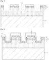
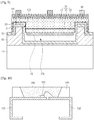
- FIG. 1 is a view showing a light-emitting device according to the embodiment.
- the light-emitting device includes a light-emitting structure 10, a reflective electrode 17 and an electrode 80.
- the light-emitting structure 10 includes a first conductive semiconductor layer 11, an active layer 12, and a second conductive semiconductor layer 13.
- the active layer 12 is interposed between the first conductive semiconductor layer 11 and the second conductive semiconductor layer 13.
- the active layer 12 is provided under the first conductive semiconductor layer 11, and the second conductive semiconductor layer 13 is provided under the active layer 12.
- the first conductive semiconductor layer 11 may include an N-type semiconductor layer doped with N-type dopants serving as first conductive dopants
- the second conductive semiconductor layer 13 may include a P-type semiconductor layer doped with P-type dopants serving as second conductive dopants
- the first conductive semiconductor layer 11 may include a P-type semiconductor layer
- the second conductive semiconductor layer 13 may include an N-type semiconductor layer.
- the first conductive semiconductor layer 11 may include an N-type semiconductor layer.
- the first conductive semiconductor layer 11 may be realized by using a compound semiconductor.
- the first conductive semiconductor layer 11 may be realized by using a group II-VI compound semiconductor, or a group III-V compound semiconductor.
- the first conductive first semiconductor layer 11 may be realized by using a semiconductor material having a compositional formula of In x Al y Ga 1-x-y N (0 ⁇ x ⁇ 1, 0 ⁇ y ⁇ 1, 0 ⁇ x+y ⁇ 1).
- the first conductive first semiconductor layer 11 may include one selected from the group consisting of GaN, A1N, AlGaN, InGaN, InN, InAlGaN, AlInN, AlGaAs, GaP, GaAs, GaAsP, and AlGaInP doped with N-type dopants such as Si, Ge, Sn, Se, and Te.
- the active layer 12 emits light having a wavelength corresponding to the energy band gap difference according to materials constituting the active layer 12 through the combination of electrons (or holes) injected through the first conductive semiconductor layer 11 and holes (or electrons) injected through the second conductive semiconductor layer 13.
- the active layer 12 may have one of a single quantum well (SQW) structure, a multi-quantum well (MQW) structure, a quantum dot structure, and a quantum wire structure, but the embodiment is not limited thereto.
- the active layer 12 may be realized by using a compound semiconductor.
- the active layer 12 may be realized by using a semiconductor material having a compositional formula of InxAlyGal-x-yN (0 ⁇ x ⁇ 1,0 ⁇ y ⁇ 1, 0 ⁇ x+y ⁇ 1).
- the active layer 12 may be formed by stacking a plurality of well layers and a plurality of barrier layers.
- the active layer 12 may have a cycle of InGaN well layer/GaN barrier layer.
- the second conductive semiconductor layer 13 may include a P-type semiconductor layer.
- the second conductive semiconductor layer 13 may be realized by using a compound semiconductor.
- the second conductive semiconductor layer 13 may be realized by using a group II-VI compound semiconductor, or a group III-V compound semiconductor.
- the second conductive semiconductor layer 13 may be realized by using a semiconductor material having a compositional formula of InxAlyGa1-x-yN (0 ⁇ x ⁇ 1, 0 ⁇ y ⁇ 1, 0 ⁇ x+y ⁇ 1).
- the second conductive semiconductor layer 13 may include one selected from the group consisting of GaN, A1N, AlGaN, InGaN, InN, InAlGaN, AlInN, AlGaAs, GaP, GaAs, GaAsP, and AlGaInP doped with P-type dopants such as Mg, Zn, Ca, Sr, and Ba.
- the first conductive semiconductor layer 11 may include a P-type semiconductor layer and the second conductive semiconductor layer 13 may include the N-type semiconductor layer.
- a semiconductor layer including an N-type or P-type semiconductor layer may be additionally provided under the second conductive semiconductor layer 13.
- the first light-emitting structure 10 may have at least one of an NP junction structure, a PN junction structure, an NPN junction structure, or a PNP junction structure.
- impurities may be doped into the first conductive semiconductor layer 11 and the second conductive semiconductor layer 13 with uniform or non-uniform doping concentration.
- the first light-emitting structure 10 may have various structures, and the embodiment is not limited thereto.
- a first conductive InGaN/GaN superlattice structure or InGaN/InGaN superlattice structure may be formed between the first conductive semiconductor layer 11 and the active layer 12.
- a second conductive AlGaN layer may be formed between the second conductive semiconductor layer 13 and the active layer 13.
- the reflective electrode 17 is disposed under the light-emitting structure 10.
- a first region 17A of the reflective electrode 17 is disposed under the second conductive semiconductor layer 13.
- a second region 17B of the reflective electrode 17 extends from the first region 17A.
- a third region 17C of the reflective electrode 17 extends from the second region 17B.
- the third region 17C of the reflective electrode 17 is an uppermost layer of the reflective electrode 17.
- the second region 17B of the reflective electrode 17 extends upward from the first region 17A.
- the second region 17B of the reflective electrode 17 extends from the first region 17A to pass through the second conductive semiconductor layer 13.
- the second region 17B of the reflective electrode 17 extends from the first region 17A to pass through the active layer 12.
- the third region 17C of the reflective electrode 17 may be disposed in the first conductive semiconductor layer 11.
- the uppermost layer of the reflective electrode 17 may be disposed in the first conductive semiconductor layer 11.
- the second region 17B of the reflective electrode 17 may reflect light, which is emitted from the active layer 12, in the upward direction.
- the second region 17B of the reflective electrode 17 may surround the active layer 12.
- the second region 17B of the reflective electrode 17 may surround the second conductive semiconductor layer 13.
- the reflective electrode 17 is electrically connected to the second conductive semiconductor layer 13. A portion of the reflective electrode 17 may make contact with the second conductive semiconductor layer 13. A portion of the reflective electrode 17 may make contact with a bottom surface of the second conductive semiconductor layer 13.
- An insulating layer 30 may be disposed between the second region 17B of the reflective electrode 17 and the first conductive semiconductor layer 11.
- the insulating layer 30 may be disposed on a top surface of the second region 17B of the reflective electrode 17.
- the insulating layer 30 may be disposed on a lateral side of the second region 17B of the reflective electrode 17.
- the insulating layer 30 may make contact with a lateral side of the second region 17B of the reflective electrode 17.
- the insulating layer 30 may be disposed between the reflective electrode 17 and the active layer 12.
- the insulating layer 30 may be disposed between the second region 17B of the reflective electrode 17 and the active layer 12.
- the insulating layer 30 may be formed of oxide or nitride.
- the insulating layer 30 may include an insulating ion implantation layer.
- the insulating layer 30 may be formed by implanting Ar, O and N ions through the implantation process.
- An ohmic contact layer 15 may be disposed between the reflective electrode 17 and the second conductive semiconductor layer 13.
- the ohmic contact layer 15 may be disposed between the first region 17A of the reflective electrode 17 and the second conductive semiconductor layer 13.
- the ohmic contact layer 15 may come into ohmic-contact with the light-emitting structure 10.
- the reflective electrode 17 may reflect light incident thereto from the light-emitting structure 10 to increase the quantity of light extracted to an outside.
- the ohmic contact layer 15 may include transparent conductive oxide.
- the ohmic contact layer 15 may include at least one selected from the group consisting of an ITO (Indium Tin Oxide), an IZO (Indium Zinc Oxide), an AZO (Aluminum Zinc Oxide), an AGZO (Aluminum Gallium Zinc Oxide), an IZTO (Indium Zinc Tin Oxide), an IAZO (Indium Aluminum Zinc Oxide), an IGZO (Indium Gallium Zinc Oxide), an IGTO (Indium Gallium Tin Oxide), an ATO (Antimony Tin Oxide), a GZO (Gallium Zinc Oxide), an IZON (IZO Nitride), ZnO, IrOx, RuOx, NiO, Pt and Ag.
- the reflective electrode 17 may include a material having high reflectance.
- the reflective electrode 17 may include a metal including at least one of Ag, Ni, Al, Rh, Pd, Ir, Ru, Mg, Zn, Pt, Cu, Au, and Hf, or an alloy thereof.
- the reflective electrode 17 may be formed in a multi-layer of the metal or the alloy thereof and a transmissive conductive material such as an ITO (Indium-Tin-Oxide), an IZO (Indium-Zinc-Oxide), an IZTO (Indium-Zinc-Tin-Oxide), an IAZO (Indium-Aluminum-Zinc-Oxide), an IGZO (Indium-Gallium-Zinc-Oxide), an IGTO (Indium-Gallium-Tin-Oxide), an AZO (Aluminum-Zinc-Oxide), or an ATO (Antimony-Tin-Oxide).
- the reflective electrode 17 may include at least one of Ag, Al, an Ag-Pd-Cu alloy, and an Ag-Cu alloy.
- the light-emitting device includes a metal layer 50 disposed under the reflective electrode 17.
- the metal layer 50 makes contact with the first region 17A of the reflective electrode 17.
- the metal layer 50 makes contact with a bottom surface of the first region 17A of the reflective electrode 17.
- the metal layer 50 makes contact with the second region 17B of the reflective electrode 17.
- the metal layer 50 makes contact with a lateral side of the second region 17B of the reflective electrode 17.
- a first region of the metal layer 50 is higher than the active layer 12.
- a top surface of the metal layer 50 is higher than the active layer 12.
- a second region of the metal layer 50 makes contact with a bottom surface of the second conductive semiconductor layer 13.
- a third region of the metal layer 50 laterally extends outward from the second region.
- the third region of the metal layer 50 is laterally exposed from a lower peripheral portion of the light-emitting structure 10.
- the metal layer 50 is disposed around a lower portion of the light-emitting structure 10 to form a metal channel layer.
- the light-emitting device according to the embodiment may have superior electric and structural reliability.
- the exposed metal layer 50 may have a width in the range of 30 ⁇ m to 40 ⁇ m.
- the width of the metal layer 50 laterally exposed from a lower peripheral portion of the light emitting structure 10 may be 35 ⁇ m.
- the metal layer 50 may include at least one of Cu, Ni, Ti, Ti-W, Cr, W, Pt, V, Fe, and Mo.
- the metal layer 50 may serve as a diffusion barrier layer.
- a bonding layer 60 and a support member 70 may be disposed under the metal layer 50.
- the metal layer 50 may prevent a material included in the bonding layer 60 from being diffused to the reflective electrode 17 in the process of providing the bonding layer 60.
- the metal layer 50 may prevent a material, such as Sn, included in the bonding layer 60 from exerting an influence upon the reflective electrode 17.
- the bonding layer 60 may include barrier metal or bonding metal.
- the bonding layer 60 may include at least one of Ti, Au, Sn, Ni, Cr, Ga, In, Bi, Cu, Ag, Nb, Pd and Ta.
- the support member 70 may support the light-emitting structure 10 according to the embodiment while performing a heat radiation function.
- the bonding layer 60 may be realized in the form of a seed layer.
- the support member 70 may include at least one of semiconductor substrates (e.g., Si, Ge, GaN, GaAs, ZnO, SiC, and SiGe substrates) implanted with Ti, Cr, Ni, Al, Pt, Au, W, Cu, Mo, Cu-W, or impurities.
- the support member 70 may be formed of insulating material.
- the light-emitting device includes the electrode 80 electrically connected to the first conductive semiconductor layer 11.
- the electrode 80 may be formed on the first conductive semiconductor layer 11.
- the electrode 80 may include an ohmic layer, an intermediate layer, and an upper layer.
- the ohmic layer may include a material selected from the group consisting of Cr, V, W, Ti, and Zn to realize ohmic contact.
- the intermediate layer may be realized by using a material selected from the group consisting of Ni, Cu, and Al.
- the upper layer may include Au.
- the electrode 80 may include at least one of Cr, V, W, Ti, Zn, Cu, Al and Au.
- a roughness may be formed on a top surface of the light-emitting structure 10.
- a light extraction pattern may be provided on the top surface of the light-emitting structure 10.
- a concavo-convex pattern may be provided on the top surface of the light-emitting structure 10.
- the light extraction pattern provided on the light-emitting structure 10 may be formed through a PEC (photo electro chemical) etching process. Therefore, according to the embodiment, the light extraction effect to the outside can be increased.
- the third region 17C of the reflective electrode 17, which extends from the second region 17B of the reflective electrode 17, may overlap with the electrode 80 in the vertical direction.
- the third region 17C of the reflective electrode 17 may serve as an uppermost layer of the reflective electrode 17.
- the uppermost layer of the reflective electrode 17 may have a width one to four times greater than a width of the electrode 80.
- the electrode may have a width in the range of 15 ⁇ m to 18 ⁇ m.
- the uppermost layer of the reflective electrode 17 may have a width in the range of 15 ⁇ m to 70 ⁇ m.
- the uppermost layer of the reflective electrode 17 may have a width in the range of 30 ⁇ m to 55 ⁇ m.
- the first region 17A of the reflective electrode 17 may be disposed under the light-emitting structure 10, and the second region 17B of the reflective electrode 17 may surround the active layer 12.
- the light emitted from the active layer 12 may be reflected from the second region 17B of the reflective electrode 17 so that the light can be extracted upward. Therefore, according to the embodiment, the orientation angle of the light can be controlled and the light extraction efficiency can be improved in the upward direction.
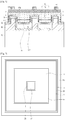
- FIGS. 2 and 3 are plan views taken along line A-A of the vertical light-emitting diode shown in FIG. 1 .
- the light emitting device includes the reflective electrode 17 disposed at an outer peripheral portion and a center portion of the light-emitting device.
- the insulating layer 30 may be disposed around the reflective electrode 17.
- the insulating layer 30 may include an insulating ion implantation layer and may electrically insulate the reflective electrode 17 from the first conductive semiconductor layer 11.
- the metal layer 50 is disposed at an edge area of the light-emitting device.
- the metal layer 50 is disposed around a lower portion of the light-emitting structure 10.
- the light emitting device includes the reflective electrode 17 disposed at an outer peripheral portion of the light-emitting device.
- a portion of the reflective electrode 17 having a predetermined line width may be disposed at the center of the light-emitting device.
- the insulating layer 30 may be disposed around the reflective electrode 17.
- the insulating layer 30 may include an insulating ion implantation layer and may electrically insulate the reflective electrode 17 from the first conductive semiconductor layer 11.
- the reflective electrode 17 may surround the first conductive semiconductor layer 11.
- the metal layer 50 may be disposed at an edge area of the light-emitting device.
- the metal layer 50 is disposed around a lower portion of the light-emitting structure 10.
- the first conductive semiconductor layer 11, the active layer 12, and the second conductive semiconductor layer 13 may be formed on a substrate 5.
- the first conductive semiconductor layer 11, the active layer 12, and the second conductive semiconductor layer 13 may be defined as the light-emitting structure 10
- the substrate 5 may include at least one of a sapphire substrate (Al 2 O 3 ), SiC, GaAs, GaN, ZnO, Si, GaP, InP, and Ge, but the embodiment is not limited thereto.
- a buffer layer may be interposed between the first conductive semiconductor layer 11 and the substrate 5.
- the first conductive semiconductor layer 11 may include an N-type semiconductor layer doped with N-type dopants serving as first conductive dopants
- the second conductive semiconductor layer 13 may include a P-type semiconductor layer doped with P-type dopants serving as second conductive dopants
- the first conductive semiconductor layer 11 may include a P-type semiconductor layer
- the second conductive semiconductor layer 13 may include an N-type semiconductor layer.
- the first conductive semiconductor layer 11 may include an N-type semiconductor.
- the first conductive semiconductor layer 11 may include a semiconductor material having a compositional formula of In x Al y Ga 1-x-y N (0 ⁇ x ⁇ 1, 0 ⁇ y ⁇ 1, 0 ⁇ x+y ⁇ 1).
- the first conductive semiconductor layer 11 may include one selected from the group consisting of InAlGaN, GaN, AlGaN, AlInN, InGaN, A1N, and InN, and may be doped with N-type dopants such as Si, Ge, Sn, Se, and Te.
- the active layer 12 emits light having a wavelength corresponding to the energy band gap difference according to materials constituting the active layer 12 through the combination of electrons (or holes) injected through the first conductive semiconductor layer 11 and holes (or electrons) injected through the second conductive semiconductor layer 13.
- the active layer 12 may have one of a single quantum well (SQW) structure, a multi-quantum well (MQW) structure, a quantum dot structure, and a quantum wire structure, but the embodiment is not limited thereto.
- the active layer 12 may be realized by using a semiconductor material having a compositional formula of In x Al y Ga 1-x-y N (0 ⁇ x ⁇ 1, 0 ⁇ y ⁇ 1, 0 ⁇ x+y ⁇ 1).
- the active layer 12 may be formed by stacking a plurality of well layers and a plurality of barrier layers.
- the active layer 12 may have a cycle of InGaN well layer/GaN barrier layer.
- the second conductive semiconductor layer 13 may be realized by using a P type semiconductor.
- the second conductive semiconductor layer 13 may be realized by using a semiconductor material having a compositional formula of In x Al y Ga 1-x-y N (0 ⁇ x ⁇ 1, 0 ⁇ y ⁇ 1, 0 ⁇ x+y ⁇ 1).
- the second conductive semiconductor layer 13 may include one selected from the group consisting of InAlGaN, GaN, AlGaN, InGaN, AlInN, A1N, and InN, and may be doped with P-type dopants such as Mg, Zn, Ca, Sr, and Ba.
- the first conductive semiconductor layer 11 may include a P-type semiconductor layer and the second conductive semiconductor layer 13 may include the N-type semiconductor layer.
- a semiconductor layer including an N-type or P-type semiconductor layer may be additionally provided on the second conductive semiconductor layer 13.
- the light-emitting structure 10 may have at least one of an NP junction structure, a PN junction structure, an NPN junction structure, or a PNP junction structure.
- impurities may be doped into the first conductive semiconductor layer 11 and the second conductive semiconductor layer 13 with uniform or non-uniform doping concentration.
- the light-emitting structure 10 may have various structures, and the embodiment is not limited thereto.
- a first conductive InGaN/GaN superlattice structure or InGaN/InGaN superlattice structure may be formed between the first conductive semiconductor layer 11 and the active layer 12.
- a second conductive AlGaN layer may be formed between the second conductive semiconductor layer 13 and the active layer 12.
- a trench 33 may be formed in the light-emitting structure 10.
- the trench 33 may be formed through a mesa etching process.
- the trench 33 may be formed through the second conductive semiconductor layer 13 and the active layer 12.
- the trench 33 may be formed by partially etching the first conductive semiconductor layer 11.
- the insulating layer 30 may be formed in the region of the trench 33.
- the insulating layer 30 may be formed of oxide or nitride.
- the insulating layer 30 may include an insulating ion implantation layer.
- the insulating layer 30 may be formed by implanting Ar, O and N ions through the implantation process.
- the ohmic contact layer 15 and the reflective electrode 17 may be disposed on the light emitting structure 10.
- the ohmic contact layer 15 may be formed on the second conductive semiconductor layer 13.
- the reflective electrode 17 may be formed on the insulating layer 30.
- the reflective electrode 17 may be formed in the trench 33.
- One portion of the reflective electrode 17 may be formed on the second conductive semiconductor layer 13.
- the other portion of the reflective electrode 17 may be formed on the ohmic contact layer 15.
- the ohmic contact layer 15 may include a transparent conductive oxide layer.
- the ohmic contact layer 15 may include at least one selected from the group consisting of an ITO (Indium Tin Oxide), an IZO (Indium Zinc Oxide), an AZO (Aluminum Zinc Oxide), an AGZO (Aluminum Gallium Zinc Oxide), an IZTO (Indium Zinc Tin Oxide), an IAZO (Indium Aluminum Zinc Oxide), an IGZO (Indium Gallium Zinc Oxide), an IGTO (Indium Gallium Tin Oxide), an ATO (Antimony Tin Oxide), a GZO (Gallium Zinc Oxide), an IZON (IZO Nitride), ZnO, IrOx, RuOx, NiO, Pt and Ag.
- the reflective electrode 17 may include a material having high reflectance.
- the reflective electrode 17 may include a metal including at least one of Ag, Ni, Al, Rh, Pd, Ir, Ru, Mg, Zn, Pt, Cu, Au, and Hf, or an alloy thereof.
- the reflective electrode 17 may be formed in a multi-layer of the metal or the alloy thereof and a transmissive conductive material such as an ITO (Indium-Tin-Oxide), an IZO (Indium-Zinc-Oxide), an IZTO (Indium-Zinc-Tin-Oxide), an IAZO (Indium-Aluminum-Zinc-Oxide), an IGZO (Indium-Gallium-Zinc-Oxide), an IGTO (Indium-Gallium-Tin-Oxide), an AZO (Aluminum-Zinc-Oxide), or an ATO (Antimony-Tin-Oxide).
- the reflective electrode 17 may include at least one of Ag, Al, an Ag-Pd-Cu alloy, and an Ag-Cu alloy.
- the metal layer 50, the bonding layer 60 and the support member 70 may be formed on the reflective layer 17.
- the metal layer 50 may include at least one of Cu, Ni, Ti, Ti-W, Cr, W, Pt, V, Fe, and Mo.
- the metal layer 50 may prevent a material included in the bonding layer 60 from being diffused to the reflective electrode 17 in the process of providing the bonding layer 60.
- the metal layer 50 may prevent a material, such as Sn, included in the bonding layer 60 from exerting an influence upon the reflective electrode 17.
- the bonding layer 60 may include barrier metal or bonding metal.
- the bonding layer 60 may include at least one of Ti, Au, Sn, Ni, Cr, Ga, In, Bi, Cu, Ag, Nb, Pd and Ta.
- the support member 70 may support the light-emitting structure 10 according to the embodiment while performing a heat radiation function.
- the bonding layer 60 may be realized in the form of a seed layer.
- the support member 70 may include at least one of semiconductor substrates (e.g., Si, Ge, GaN, GaAs, ZnO, SiC, and SiGe substrates) implanted with Ti, Cr, Ni, Al, Pt, Au, W, Cu, Mo, Cu-W, or impurities.
- the support member 70 may be formed of an insulating material.
- the substrate 5 is removed from the first conductive semiconductor layer 11.
- the substrate 5 may be removed through a laser lift off (LLO) process.
- LLO process is a process to delaminate the substrate 5 from the first conductive semiconductor layer 11 by irradiating a laser to the bottom surface of the substrate 5.
- the lateral side of the light-emitting structure 10 is etched through an isolation etching process to expose a portion of the metal layer 50.
- the isolation etching process may be performed through a dry etching process such as an inductively coupled plasma (ICP) process, but the embodiment is not limited thereto.
- ICP inductively coupled plasma
- a roughness may be formed on a top surface of the light-emitting structure 10.
- a light extraction pattern may be provided on the top surface of the light-emitting structure 10.
- a concavo-convex pattern may be provided on the top surface of the light-emitting structure 10.
- the light extraction pattern provided on the light-emitting structure 10 may be formed through a PEC (photo electro chemical) etching process. Therefore, according to the embodiment, the light extraction effect to the outside can be increased.
- the electrode 80 may be formed on the light-emitting structure 10.
- the electrode 80 may be electrically connected to the first conductive semiconductor layer 11. A portion of the electrode 80 may make contact with the first conductive semiconductor layer 11. According to the embodiment, power may be applied to the light-emitting structure 10 through the reflective electrode 17 and the electrode 80.
- the electrode 80 may include an ohmic layer, an intermediate layer, and an upper layer.
- the ohmic layer may include a material selected from the group consisting of Cr, V, W, Ti, and Zn to realize ohmic contact.
- the intermediate layer may be realized by using a material selected from the group consisting of Ni, Cu, and Al.
- the upper layer may include Au.
- the electrode 80 may include at least one of Cr, V, W, Ti, Zn, Cu, Al and Au.
- the reflective electrode 17 is disposed under the light-emitting structure 10.
- a first region 17A of the reflective electrode 17 is disposed under the second conductive semiconductor layer 13.
- a second region 17B of the reflective electrode 17 extends from the first region 17A.
- a third region 17C of the reflective electrode 17 may extend from the second region 17B.
- the third region 17C of the reflective electrode 17 is an uppermost layer of the reflective electrode 17.
- the second region 17B of the reflective electrode 17 extends upward from the first region 17A.
- the second region 17B of the reflective electrode 17 extends from the first region 17A to pass through the second conductive semiconductor layer 13.
- the second region 17B of the reflective electrode 17 extends from the first region 17A to pass through the active layer 12.
- the third region 17C of the reflective electrode 17 may be disposed in the first conductive semiconductor layer 11.
- the uppermost layer of the reflective electrode 17 may be disposed in the first conductive semiconductor layer 11.
- the second region 17B of the reflective electrode 17 may reflect light, which is emitted from the active layer 12, in the upward direction.
- the second region 17B of the reflective electrode 17 may surround the active layer 12.
- the second region 17B of the reflective electrode 17 may surround the second conductive semiconductor layer 13.
- the reflective electrode 17 is electrically connected to the second conductive semiconductor layer 13. A portion of the reflective electrode 17 may make contact with the second conductive semiconductor layer 13. A portion of the reflective electrode 17 may make contact with a bottom surface of the second conductive semiconductor layer 13.
- An insulating layer 30 may be disposed between the second region 17B of the reflective electrode 17 and the first conductive semiconductor layer 11.
- the insulating layer 30 may be disposed on a top surface of the second region 17B of the reflective electrode 17.
- the insulating layer 30 may be disposed on a lateral side of the second region 17B of the reflective electrode 17.
- the insulating layer 30 may make contact with a lateral side of the second region 17B of the reflective electrode 17.
- the insulating layer 30 may be disposed between the reflective electrode 17 and the active layer 12.
- the insulating layer 30 may be disposed between the second region 17B of the reflective electrode 17 and the active layer 12.
- An ohmic contact layer 15 may be disposed between the reflective electrode 17 and the second conductive semiconductor layer 13.
- the ohmic contact layer 15 may be disposed between the first region 17A of the reflective electrode 17 and the second conductive semiconductor layer 13.
- the ohmic contact layer 15 may come into ohmic-contact with the light-emitting structure 10.
- the reflective electrode 17 may reflect light incident thereto from the light-emitting structure 10 to increase the quantity of light extracted to an outside.
- the light-emitting device includes a metal layer 50 disposed under the reflective electrode 17.
- the metal layer 50 makes contact with the first region 17A of the reflective electrode 17.
- the metal layer 50 makes contact with a bottom surface of the first region 17A of the reflective electrode 17.
- the metal layer 50 makes contact with the second region 17B of the reflective electrode 17.
- the metal layer 50 makes contact with a lateral side of the second region 17B of the reflective electrode 17.
- a first region of the metal layer 50 is higher than the active layer 12.
- a top surface of the metal layer 50 is higher than the active layer 12.
- a second region of the metal layer 50 makes contact with a bottom surface of the second conductive semiconductor layer 13.
- a third region of the metal layer 50 laterally extends outward from the second region.
- the third region of the metal layer 50 is laterally exposed from a lower peripheral portion of the light-emitting structure 10.
- the metal layer 50 is disposed around a lower portion of the light-emitting structure 10 to form a metal channel layer.
- the light-emitting device according to the embodiment may have superior electric and structural reliability.
- the exposed metal layer 50 may have a width in the range of 30 ⁇ m to 40 ⁇ m.
- the width of the metal layer 50 laterally exposed from a lower peripheral portion of the light emitting structure 10 may be 35 ⁇ m.
- the third region 17C of the reflective electrode 17 serves as an uppermost layer of the reflective electrode 17.
- the uppermost layer of the reflective electrode 17 may have a width one to four times greater than a width of the electrode 80.
- the electrode may have a width in the range of 15 ⁇ m to 18 ⁇ m.
- the uppermost layer of the reflective electrode 17 may have a width in the range of 15 ⁇ m to 70 ⁇ m.
- the uppermost layer of the reflective electrode 17 may have a width in the range of 30 ⁇ m to 55 ⁇ m.
- the first region 17A of the reflective electrode 17 is disposed under the light-emitting structure 10, and the second region 17B of the reflective electrode 17 may surround the active layer 12.
- the light emitted from the active layer 12 may be reflected from the second region 17B of the reflective electrode 17 so that the light can be extracted upward. Therefore, according to the embodiment, the orientation angle of the light can be controlled and the light extraction efficiency can be improved in the upward direction.
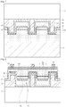
- FIG. 9 is a view showing another example of a light-emitting device according to the embodiment.
- components and structures the same as those described with reference to FIG. 1 will not be further described in order to avoid redundancy.
- the light-emitting device includes the reflective electrode 17 disposed at an outer peripheral portion of the light-emitting structure 10.
- FIG. 1 shows the uppermost surface 17C of the reflective electrode 17 disposed on the center region of the light-emitting structure 10.
- the third region 17C of the reflective electrode 17 may not protrude on the center region of the light-emitting structure 10.
- the reflective electrode 17 is disposed under the light-emitting structure 10.
- a first region 17A of the reflective electrode 17 is disposed under the second conductive semiconductor layer 13.
- a second region 17B of the reflective electrode 17 extends from the first region 17A.
- a third region 17C of the reflective electrode 17 extends from the second region 17B.
- the third region 17C of the reflective electrode 17 is an uppermost layer of the reflective electrode 17.
- the second region 17B of the reflective electrode 17 extends upward from the first region 17A.
- the second region 17B of the reflective electrode 17 extends from the first region 17A to pass through the second conductive semiconductor layer 13.
- the second region 17B of the reflective electrode 17 extends from the first region 17A to pass through the active layer 12.
- the third region 17C of the reflective electrode 17 is disposed in the first conductive semiconductor layer 11.
- the uppermost layer of the reflective electrode 17 may be disposed in the first conductive semiconductor layer 11.
- the second region 17B of the reflective electrode 17 may reflect light, which is emitted from the active layer 12, in the upward direction.
- the second region 17B of the reflective electrode 17 may surround the active layer 12.
- the second region 17B of the reflective electrode 17 may surround the second conductive semiconductor layer 13.
- the reflective electrode 17 is electrically connected to the second conductive semiconductor layer 13. A portion of the reflective electrode 17 may make contact with the second conductive semiconductor layer 13. A portion of the reflective electrode 17 may make contact with a bottom surface of the second conductive semiconductor layer 13.
- An insulating layer 30 may be disposed between the second region 17B of the reflective electrode 17 and the first conductive semiconductor layer 11.
- the insulating layer 30 may be disposed on a top surface of the second region 17B of the reflective electrode 17.
- the insulating layer 30 may be disposed on a lateral side of the second region 17B of the reflective electrode 17.
- the insulating layer 30 may make contact with a lateral side of the second region 17B of the reflective electrode 17.
- the insulating layer 30 may be disposed between the reflective electrode 17 and the active layer 12.
- the insulating layer 30 may be disposed between the second region 17B of the reflective electrode 17 and the active layer 12.
- An ohmic contact layer 15 may be disposed between the reflective electrode 17 and the second conductive semiconductor layer 13.
- the ohmic contact layer 15 may be disposed between the first region 17A of the reflective electrode 17 and the second conductive semiconductor layer 13.
- the ohmic contact layer 15 may come into ohmic-contact with the light-emitting structure 10.
- the reflective electrode 17 may reflect light incident thereto from the light-emitting structure 10 to increase the quantity of light extracted to an outside.
- the light-emitting device includes a metal layer 50 disposed under the reflective electrode 17.
- the metal layer 50 makes contact with the first region 17A of the reflective electrode 17.
- the metal layer 50 makes contact with a bottom surface of the first region 17A of the reflective electrode 17.
- the metal layer 50 makes contact with the second region 17B of the reflective electrode 17.
- the metal layer 50 makes contact with a lateral side of the second region 17B of the reflective electrode 17.
- a first region of the metal layer 50 is higher than the active layer 12.
- a top surface of the metal layer 50 is higher than the active layer 12.
- a second region of the metal layer 50 makes contact with a bottom surface of the second conductive semiconductor layer 13.
- a third region of the metal layer 50 laterally extends outward from the second region.
- the third region of the metal layer 50 is laterally exposed from a lower peripheral portion of the light-emitting structure 10.
- the metal layer 50 is disposed around a lower portion of the light-emitting structure 10 to form a metal channel layer.
- the light-emitting device according to the embodiment may have superior electric and structural reliability.
- the exposed metal layer 50 may have a width in the range of 30 ⁇ m to 40 ⁇ m.
- the width of the metal layer 50 laterally exposed from a lower peripheral portion of the light emitting structure 10 may be 35 ⁇ m.
- the third region 17C of the reflective electrode 17 serves as an uppermost layer of the reflective electrode 17.
- the uppermost layer of the reflective electrode 17 may have a width one to four times greater than a width of the electrode 80.
- the electrode may have a width in the range of 15 ⁇ m to 18 ⁇ m.
- the uppermost layer of the reflective electrode 17 may have a width in the range of 15 ⁇ m to 70 ⁇ m.
- the uppermost layer of the reflective electrode 17 may have a width in the range of 30 ⁇ m to 55 ⁇ m.
- the first region 17A of the reflective electrode 17 is disposed under the light-emitting structure 10, and the second region 17B of the reflective electrode 17 may surround the active layer 12.
- the light emitted from the active layer 12 may be reflected from the second region 17B of the reflective electrode 17 so that the light can be extracted upward. Therefore, according to the embodiment, the orientation angle of the light can be controlled and the light extraction efficiency can be improved in the upward direction.
- FIG. 10 is a view showing a light-emitting device package to which the light-emitting device according to the embodiment is applied.
- the light-emitting device package may include a body 120, first and second lead electrodes 131 and 132 formed on the body 120, a light-emitting device 100 provided on the body 120 and electrically connected to the first and second lead electrodes 131 and 132 and a molding member 140 that surrounds the light-emitting device 100.
- the body 120 may include silicon, synthetic resin or metallic material, and an inclined surface may be formed in the vicinity of the light-emitting device 100.
- the first and second lead electrodes 131 and 132 are electrically isolated from each other to supply power to the light-emitting device 100.
- the first and second lead electrodes 131 and 132 can improve the light efficiency by reflecting the light emitted from the light-emitting device 100. Further, the first and second lead electrodes 131 and 132 may dissipate heat generated from the light-emitting device 100 to the outside.
- the light-emitting device 100 can be installed on the body 120 or the first or second lead electrode 131 or 132.
- the light-emitting device 100 may be electrically connected to the first and second lead electrodes 131 and 132 through one of a wire scheme, a flip-chip scheme, and a die-bonding scheme.
- the molding member 140 may surround the light-emitting device 100 to protect the light-emitting device 100.
- the molding member 140 may include phosphors to change the wavelength of the light emitted from the light-emitting device 100.
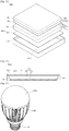
- a plurality of light-emitting devices according to an embodiment of the invention or light-emitting device packages may be arrayed on a substrate, and an optical member including a lens, a light guide plate, a prism sheet, or a diffusion sheet may be provided on the optical path of the light emitted from the light-emitting device package.
- the light-emitting device package, the substrate, and the optical member may serve as a light unit.
- the light unit is realized in a top view type or a side view type and variously provided in display devices of a portable terminal and a laptop computer or a lighting apparatus and an indicator apparatus.
- a lighting apparatus can include a light-emitting device according to an embodiment of the invention, or a light-emitting device package according to the embodiment.
- the lighting apparatus may include a lamp, a signal lamp, an electric sign board and a headlight of a vehicle.
- the light-emitting device may be applied to the light unit.
- the light unit has a structure in which a plurality of light-emitting devices are arrayed.
- the light unit may include a display device as shown in FIGS. 11 and 12 and the lighting apparatus as shown in FIGS. 13 to 17 .
- a display device 1000 includes a light guide plate 1041, a light-emitting module 1031 for supplying the light to the light guide plate 1041, a reflective member 1022 provided below the light guide plate 1041, an optical sheet 1051 provided above the light guide plate 1041, a display panel 1061 provided above the optical sheet 1051, and a bottom cover 1011 for receiving the light guide plate 1041, the light-emitting module 1031, and the reflective member 1022.
- the embodiment is not limited to the above structure.
- the bottom cover 1011, the reflective member 1022, the light guide plate 1041 and the optical sheet 1051 may constitute a light unit 1050.
- the light guide plate 1041 diffuses the light to provide surface light.
- the light guide plate 1041 may include transparent material.
- the light guide plate 1041 may include one of acryl-based resin, such as PMMA (polymethyl methacrylate), PET (polyethylene terephthalate), PC (polycarbonate), COC (cyclic olefin copolymer) and PEN (polyethylene naphthalate) resin.
- PMMA polymethyl methacrylate
- PET polyethylene terephthalate
- PC polycarbonate
- COC cyclic olefin copolymer
- PEN polyethylene naphthalate
- the light-emitting module 1031 supplies the light to at least one side of the light guide plate 1041.
- the light-emitting module 1031 serves as the light source of the display device.
- At least one light-emitting module 1031 is provided to directly or indirectly supply the light from one side of the light guide plate 1041.
- the light-emitting module 1031 may include a substrate 1033 and light-emitting devices 100 according to an embodiment of the invention or the light-emitting device package 200 described above.
- the light-emitting packages 200 may be arrayed on the substrate 1033 while being spaced apart from each other at the predetermined interval.
- the substrate 1033 may be a printed circuit board (PCB) including a circuit pattern.
- the substrate 1033 may also include a metal core PCB (MCPCB) or a flexible PCB (FPCB) as well as the PCB, but the embodiment is not limited thereto. If the light-emitting device packages 200 are installed on the lateral side of the bottom cover 1011 or on a heat dissipation plate, the substrate 1033 may be omitted. The heat dissipation plate may partially make contact with the top surface of the bottom cover 1011.
- the light-emitting device packages 200 are installed such that light exit surfaces of the light-emitting device packages 200 are spaced apart from the light guide plate 1041 at a predetermined distance, but the embodiment is not limited thereto.
- the light-emitting device packages 200 may directly or indirectly supply the light to a light incident part, which is one side of the light guide plate 1041, but the embodiment is not limited thereto.
- the reflective member 1022 may be disposed below the light guide plate 1041.
- the reflective member 1022 reflects the light, which travels downward through the bottom surface of the light guide plate 1041, upward, thereby improving the brightness of the light unit 1050.
- the reflective member 1022 may include PET, PC or PVC resin, but the embodiment is not limited thereto.
- the reflective member 1022 may serve as the top surface of the bottom cover 1011, but the embodiment is not limited thereto.
- the bottom cover 1011 may receive the light guide plate 1041, the light-emitting module 1031, and the reflective member 1022 therein. To this end, the bottom cover 1011 has a receiving section 1012 having a box shape with an opened top surface, but the embodiment is not limited thereto. The bottom cover 1011 can be coupled with the top cover (not shown), but the embodiment is not limited thereto.
- the bottom cover 1011 can be manufactured through a press process or an extrusion process by using metallic material or resin material.
- the bottom cover 1011 may include metal or non-metallic material having superior thermal conductivity, but the embodiment is not limited thereto.
- the display panel 1061 for example, is an LCD panel including first and second transparent substrates, which are opposite to each other, and a liquid crystal layer interposed between the first and second substrates.
- a polarizing plate can be attached to at least one surface of the display panel 1061, but the embodiment is not limited thereto.
- the display panel 1061 displays information by using light passing through the optical sheet 1051.
- the display device 1000 can be applied to various portable terminals, monitors of notebook computers and laptop computers, and televisions.
- the optical sheet 1051 is disposed between the display panel 1061 and the light guide plate 1041 and includes at least one transmissive sheet.
- the optical sheet 1051 includes at least one of a diffusion sheet, horizontal and vertical prism sheets, and a brightness enhanced sheet.
- the diffusion sheet diffuses the incident light
- the horizontal and/or vertical prism sheet concentrates the incident light onto a display region
- the brightness enhanced sheet improves the brightness by reusing the light to be lost.
- a protective sheet can be provided on the display panel 1061, but the embodiment is not limited thereto.
- the light guide plate 1041 and the optical sheet 1051 can be provided on the optical path of the light-emitting module 1031 as optical members, but the embodiment is not limited thereto.
- FIG. 12 is a view showing another example of a display device according to the embodiment.
- the display device 1100 includes a bottom cover 1152, a substrate 1020 on which the light-emitting devices 100 are arrayed, an optical member 1154, and a display panel 1155.
- the substrate 1020 and the light-emitting device packages 200 may constitute a light-emitting module 1060.
- a light unit may include the bottom cover 1152, at least one light-emitting module 1060, and the optical member 154.
- the bottom cover 1152 can be provided therein with a receiving section 1153, but the embodiment is not limited thereto.
- the optical member 1154 may include at least one of a lens, a light guide plate, a diffusion sheet, horizontal and vertical prism sheets, and a brightness enhanced sheet.
- the light guide plate may include PC or PMMA (Poly methyl methacrylate). The light guide plate can be omitted.
- the diffusion sheet diffuses the incident light
- the horizontal and vertical prism sheets concentrate the incident light onto a display region
- the brightness enhanced sheet improves the brightness by reusing the light to be lost.
- the optical member 1154 is disposed above the light-emitting module 1060 in order to convert the light emitted from the light-emitting module 1060 into the surface light. In addition, the optical member 1154 may diffuse or collect the light.
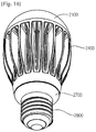
- FIGS. 13 to 15 are views showing a lighting apparatus according to the embodiment.
- FIG. 13 is a top perspective view of the lighting apparatus
- FIG. 14 is a bottom perspective view of the lighting apparatus shown in FIG. 13
- FIG. 15 is an exploded perspective view of the lighting apparatus shown in FIG. 13 .
- the lighting apparatus may include a cover 2100, a light source module 2200, a radiator 2400, a power supply part 2600, an inner case 2700, and a socket 2800.
- the lighting apparatus according to the embodiment may further include at least one of a member 2300 and a holder 2500.
- the light source module 2200 may include the light-emitting device package.
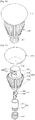
- the cover 2100 may have a blub shape or a hemispheric shape.
- the cover 2100 may have a hollow structure which is partially open.
- the cover 2100 may be optically coupled with the light source module 2200.
- the cover 2100 may diffuse, scatter, or excite light provided from the light source module 2200.
- the cover 2100 may be an optical member.
- the cover 2100 may be coupled with the radiator 2400.
- the cover 2100 may include a coupling part which is coupled with the radiator 2400.
- the cover 2100 may include an inner surface coated with a milk-white pigment.
- the milk-white pigment may include a diffusion material to diffuse light.
- the roughness of the inner surface of the cover 2100 may be greater than the roughness of the outer surface of the cover 2100. The surface roughness is provided for the purpose of sufficiently scattering and diffusing the light from the light source module 2200.
- the cover 2100 may include glass, plastic, polypropylene (PP), polyethylene (PE) or polycarbonate (PC).
- the polycarbonate (PC) has the superior light resistance, heat resistance and strength among the above materials.
- the cover 2100 may be transparent so that a user may view the light source module 2200 from the outside, or may be opaque.
- the cover 2100 may be formed through a blow molding scheme.
- the light source module 2200 may be disposed at one surface of the radiator 2400. Accordingly, the heat from the light source module 2200 is transferred to the radiator 2400.
- the light source module 2200 may include a light source 2210, a connection plate 2230, and a connector 2250.
- the member 2300 is disposed on a top surface of the radiator 2400, and includes guide grooves 2310 into which a plurality of light sources 2210 and the connector 2250 are inserted.
- the guide grooves 2310 correspond to a substrate of the light source 2210 and the connector 2250.
- a surface of the member 2300 may be coated with a light reflective material.
- the surface of the member 2300 may be coated with white pigment.
- the member 2300 reflects again light, which is reflected by the inner surface of the cover 2100 and is returned to the direction of the light source module 2200, to the direction of the cover 2100. Accordingly, the light efficiency of the lighting apparatus according to the embodiment may be improved.
- the member 2300 may include an insulating material.
- the connection plate 2230 of the light source module 2200 may include an electrically conductive material.
- the radiator 2400 may be electrically connected to the connection plate 2230.
- the member 2300 may be formed by an insulating material, thereby preventing the connection plate 2230 from being electrically shorted with the radiator 2400.
- the radiator 2400 receives heat from the light source module 2200 and the power supply part 2600 and dissipates the heat.
- the holder 2500 covers a receiving groove 2719 of an insulating part 2710 of an inner case 2700. Accordingly, the power supply part 2600 received in the insulating part 2710 of the inner case 2700 is sealed.
- the holder 2500 includes a guide protrusion 2510.
- the guide protrusion 2510 has a hole and a protrusion of the power supply part 2600 extends by passing through the hole.
- the power supply part 2600 processes or converts an electric signal received from the outside and provides the processed or converted electric signal to the light source module 2200.
- the power supply part 2600 is received in the receiving groove 2719 of the inner case 2700, and is sealed inside the inner case 2700 by the holder 2500.
- the power supply part 2600 may include a protrusion 2610, a guide part 2630, a base 2650, and an extension part 2670.
- the guide part 2630 has a shape protruding from one side of the base 2650 to the outside.
- the guide part 2630 may be inserted into the holder 2500.
- a plurality of components may be disposed on one surface of the base 2650.
- the components may include a DC converter to convert AC power provided from an external power supply into DC power, a driving chip to control the driving of the light source module 2200, and an electrostatic discharge (ESD) protection device to protect the light source module 2200, but the embodiment is not limited thereto.
- the extension part 2670 has a shape protruding from an opposite side of the base 2650 to the outside.
- the extension part 2670 is inserted into an inside of the connection part 2750 of the inner case 2700, and receives an electric signal from the outside.
- a width of the extension part 2670 may be smaller than or equal to a width of the connection part 2750 of the inner case 2700.
- First terminals of a "+ electric wire” and a "- electric wire” are electrically connected to the extension part 2670 and second terminals of the "+ electric wire” and the "- electric wire” may be electrically connected to a socket 2800.
- the inner case 2700 may include a molding part therein together with the power supply part 2600.
- the molding part is prepared by hardening molding liquid, and the power supply part 2600 may be fixed inside the inner case 2700 by the molding part.
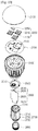
- FIGS. 16 and 17 are views showing another example of a lighting apparatus according to the embodiment.
- FIG. 16 is a perspective view of the lighting apparatus according to the embodiment and FIG. 17 is an exploded perspective view of the lighting apparatus shown in FIG. 16 .
- the lighting apparatus may include a cover 3100, a light source part 3200, a radiator 3300, a circuit part 3400, an inner case 3500, and a socket 3600.
- the light source part 3200 may include the light-emitting device according to an embodiment of the invention or the light-emitting device module.
- the cover 3100 may have a hollow blub shape.
- the cover 3100 has an opening 3110.
- the light source part 3200 and a member 3350 may be inserted through the opening 3110.
- the cover 3100 may be coupled with the radiator 3300 and may surround the light source part 3200 and the member 3350.
- the light source part 3200 and the member 3350 may be blocked from the outside by the coupling between the cover 3100 and the radiator 3300.
- the cover 3100 may be coupled with the radiator 3300 by an adhesive or various schemes such as a rotation coupling scheme and a hook coupling scheme.
- the rotation coupling scheme is a scheme where a thread of the cover 3100 is coupled with a screw groove of the radiator 3300, and the cover 3100 is coupled with the radiator 3300 by rotation of the cover 3100.
- the hook coupling scheme is a scheme where a projection of the cover 3100 is inserted into a groove of the radiator 3300 so that the cover 3100 is coupled with the radiator 3300.
- the cover 3100 may be optically coupled to the light source part 3200.
- the cover 3100 may diffuse, scatter or excite light emitted from the light-emitting device 3230.
- the cover 3100 may be a kind of optical members.
- a phosphor may be provided on inner/outer surfaces or an outer surface of the cover 3100 to excite light emitted from the light source part 3200.
- the cover 3100 may include an inner surface coated with a milk-white pigment.
- the milk-white pigment may include a diffusion material to diffuse light.
- the roughness of the inner surface of the cover 3100 may be greater than the roughness of the outer surface of the cover 3100. The surface roughness is provided for the purpose of sufficiently scattering and diffusing the light from the light source part 3200.
- the cover 3100 may include glass, plastic, polypropylene (PP), polyethylene (PE) or polycarbonate (PC).
- the polycarbonate (PC) has the superior light resistance, heat resistance and strength among the above materials.
- the cover 3100 may be transparent so that a user may view the light source part 3200 from the outside, or may be opaque.
- the cover 3100 may be formed through a blow molding scheme.
- the light source part 3200 is disposed at the member 3350 of the radiator 3300, and a plurality of light source parts 3200 may be provided.
- the light source part 3200 may be disposed on at least one of side surfaces of the member 3350.
- the light source part 3200 may be disposed at an upper portion of the side surface of the member 3350.
- the light source part 3200 may be disposed at three of six side surfaces of the member 3350. However, the embodiment is not limited thereto, and the light source part 3200 may be disposed at all side surfaces of the member 3350.
- the light source part 3200 may include a substrate 3210 and a light-emitting device 3230.
- the light-emitting device 3230 may be disposed on one surface of the substrate 3210.
- the substrate 3210 has a rectangular plate shape, but the embodiment is not limited thereto.
- the substrate 3210 may have various shapes.
- the substrate 3210 may have a circular plate shape or a polygonal plate shape.
- the substrate 3210 may be provided by printing a circuit pattern on an insulator.
- the substrate 3210 may include a typical printed circuit board (PCB), a metal core PCB, a flexible PCB, and a ceramic PCB.
- the substrate may have a COB (chips on board) type in which LED chips, which are not packaged, are directly bonded on the PCB.
- COB chips on board
- the substrate 3210 may include a material suitable to reflect light, or the surface of the substrate may have a color such as a white color or a silver color to effectively reflect the light.
- the substrate 3210 may be electrically connected to the circuit part 3400 received in the radiator 3300.
- the substrate 3210 and the circuit part 3400 may be connected to each other by a wire.
- the wire may connect the substrate 3210 and the circuit part 3400 to each other by passing through the radiator 3300.
- the light-emitting device 3230 may be a light-emitting diode chip that emits red, green, blue or UV light.
- the light-emitting diode chip is a vertical type and the light-emitting diode chip may emit blue, red, yellow or green light.
- the light-emitting device 3230 may include a luminescence material.
- the luminescence material may include at least one of garnet-based phosphors (YAG, or TAG), silicate-based phosphors, nitride-based phosphors, and oxynitride-based phosphors.
- the luminescence material may include at least one of a red luminescence material, a yellow luminescence material and a green luminescence material.
- the radiator 3300 is coupled with the cover 3100, and may radiate heat from the light source part 3200.
- the radiator 330 has a predetermined volume, and includes a top surface 3310 and a side surface 3330.
- the member 3350 may be disposed on the top surface 3310 of the radiator 3310.
- the top surface 3310 of the radiator 3300 may be coupled with the cover 3100.
- the top surface 3310 of the radiator 3300 may have a shape corresponding to an opening 3110 of the cover 3100.
- a plurality of heat radiation pins 3370 may be disposed at the side surface 3330 of the radiator 3300.
- the heat radiation pin 3370 may extend outward from the side surface 3330 of the radiator 3300 or may be connected to the side surface 3330 of the radiator 3300.
- the heat radiation pin 3370 may improve heat radiation efficiency by increasing a heat radiation area of the radiator 3300.
- the side surface 3330 may not include the heat radiation pin 3370.
- the member 3350 may be disposed on the top surface of the radiator 3300.
- the member 3350 may be integrated with or coupled to the top surface 3310 of the radiator 3300.
- the member 3350 may have the shape of a polygonal prism.
- the member 3350 may have the shape of a hexahedral prism.
- the member 3350 having the shape of a hexahedral prism includes a top surface, a bottom surface, and six side surfaces.
- the member 3350 may have the shape of a circular prism or the shape of an elliptical prism as well as the shape of a hexahedral prism.
- the substrate 3210 of the light source part 3200 may be a flexible substrate.
- the light source part 3200 may be disposed at six side surfaces of the member 3350.
- the light source part 3200 may be disposed at all or some of the six side surfaces of the member 3350.
- the light source part 3200 is disposed at three of the six side surfaces of the member 3350.
- the substrate 3210 is disposed at the side surface of the member 3350.
- the side surface of the member 3350 may be substantially vertical to the top surface 3310 of the radiator 3300. Accordingly, the substrate 3210 and the top surface 3310 of the radiator 3300 may be substantially vertical to each other.
- the member 3350 may include a material representing thermal conductivity. Thus, heat from the light source part 3200 can be rapidly transferred to the member 3350.
- the material for the member 3350 may include an alloy of metals such as aluminum (Al), nickel (Ni), copper (Cu), magnesium (Mg), silver (Ag), or tin (Sn).
- the member 3350 may include a plastic material having thermal conductivity. The plastic material having thermal conductivity is advantageous in that it is lighter than the metal and has thermal conductivity in a single direction.
- the circuit part 3400 receives power from the outside, and converts the received power suitably for the light source part 3200.
- the circuit part 3400 provides the converted power to the light source part 3200.
- the circuit part 3400 may be disposed at the radiator 3300.
- the circuit part 3400 may be received in the inner case 3500, and may be received in the radiator 3300 together with the inner case 3500.
- the circuit part 3400 may include a circuit board 3410 and a plurality of components mounted on the circuit board 3410.
- the circuit board 3410 has a circular shape, but the embodiment is not limited thereto. That is, the circuit board 3410 may have various shapes. For example, the circuit board may have an elliptical shape or a polygonal shape.
- the circuit board 3410 may be provided by printing a circuit pattern on an insulator.
- the circuit board 3410 is electrically connected to the substrate 3210 of the light source part 3200.
- the circuit part 3410 and the substrate 3210 may be connected to each other by a wire.
- the wire may be disposed inside the radiator 3300 to connect the substrate 3210 to the circuit board 3410.
- a plurality of components 3430 may include a direct current converter converting AC power provided from an external power supply into DC power, a driving chip controlling driving of the light source part 3200, and an electrostatic discharge (ESD) protective device.
- ESD electrostatic discharge
- the inner case 3500 receives the circuit part 3400 therein.
- the inner case 3500 may include a receiving part 3510 to receive the circuit part 3400.
- the receiving part 3510 may have a cylindrical shape.
- the shape of the receiving part 3510 may be changed according to the shape of the radiator 3300.
- the inner case 3500 may be received in the radiator 3300.
- the receiving part 3510 of the inner case 3500 may be received in a receiving part which is formed at a bottom surface of the radiator 3300.
- the inner case 3500 may be coupled with the socket 3600.
- the inner case 3500 may include a connecting part 3530 coupled with the socket 3600.
- the connecting part 3530 may have a thread structure corresponding to a screw groove structure of the socket 3600.
- the inner case 3500 is an insulator. Accordingly, the inner case 3500 prevents electric short between the circuit part 3400 and the radiator 3300.
- the inner case 3500 may include a plastic or resin material.
- the socket 3600 may be coupled with the inner case 3500.
- the socket 3600 may be coupled with the connecting part 3530 of the inner case 3500.
- the socket 3600 may have the structure the same as that of a conventional incandescent light bulb.
- the socket 3600 is electrically connected to the circuit part 3400.
- the circuit part 3400 and the socket 3600 may be connected to each other by a wire. If external power is applied to the socket 3600, the external power may be transferred to the circuit part 3400.
- the socket 3600 may have a screw groove structure corresponding to a thread structure of the connecting part 3550.
Landscapes
- Engineering & Computer Science (AREA)
- Manufacturing & Machinery (AREA)
- Computer Hardware Design (AREA)
- Microelectronics & Electronic Packaging (AREA)
- Power Engineering (AREA)
- Led Devices (AREA)
Applications Claiming Priority (2)
| Application Number | Priority Date | Filing Date | Title |
|---|---|---|---|
| KR1020120051745A KR101916144B1 (ko) | 2012-05-16 | 2012-05-16 | 발광소자, 발광소자 패키지 및 라이트 유닛 |
| PCT/KR2013/004185 WO2013172606A1 (ko) | 2012-05-16 | 2013-05-10 | 발광소자, 발광소자 페키지 및 라이트 유닛 |
Publications (3)
| Publication Number | Publication Date |
|---|---|
| EP2851968A1 EP2851968A1 (en) | 2015-03-25 |
| EP2851968A4 EP2851968A4 (en) | 2015-10-07 |
| EP2851968B1 true EP2851968B1 (en) | 2019-09-25 |
Family
ID=49583965
Family Applications (1)
| Application Number | Title | Priority Date | Filing Date |
|---|---|---|---|
| EP13791696.1A Active EP2851968B1 (en) | 2012-05-16 | 2013-05-10 | Light-emitting device |
Country Status (5)
| Country | Link |
|---|---|
| US (1) | US9478710B2 (ko) |
| EP (1) | EP2851968B1 (ko) |
| KR (1) | KR101916144B1 (ko) |
| CN (1) | CN104303323B (ko) |
| WO (1) | WO2013172606A1 (ko) |
Families Citing this family (6)
| Publication number | Priority date | Publication date | Assignee | Title |
|---|---|---|---|---|
| KR102156376B1 (ko) * | 2014-02-21 | 2020-09-15 | 엘지이노텍 주식회사 | 발광 소자 |
| KR102200018B1 (ko) * | 2014-06-17 | 2021-01-11 | 엘지이노텍 주식회사 | 발광소자 |
| KR102299738B1 (ko) * | 2014-12-23 | 2021-09-09 | 쑤저우 레킨 세미컨덕터 컴퍼니 리미티드 | 발광소자 및 조명시스템 |
| TWI720053B (zh) * | 2016-11-09 | 2021-03-01 | 晶元光電股份有限公司 | 發光元件及其製造方法 |
| CN111863853A (zh) * | 2019-04-24 | 2020-10-30 | 深圳第三代半导体研究院 | 一种垂直集成单元二极管芯片 |
| CN112537754B (zh) * | 2020-12-08 | 2021-10-22 | 江苏创芯海微科技有限公司 | 电隔离结构及其制备方法 |
Family Cites Families (14)
| Publication number | Priority date | Publication date | Assignee | Title |
|---|---|---|---|---|
| JP4890813B2 (ja) * | 2005-08-05 | 2012-03-07 | 昭和電工株式会社 | 発光ダイオード及び発光ダイオードランプ |
| KR101064053B1 (ko) * | 2009-02-25 | 2011-09-08 | 엘지이노텍 주식회사 | 발광소자 및 그 제조방법 |
| KR101072034B1 (ko) * | 2009-10-15 | 2011-10-10 | 엘지이노텍 주식회사 | 반도체 발광소자 및 그 제조방법 |
| KR100986407B1 (ko) * | 2009-10-22 | 2010-10-08 | 엘지이노텍 주식회사 | 발광소자 및 그 제조방법 |
| KR101007077B1 (ko) | 2009-11-06 | 2011-01-10 | 엘지이노텍 주식회사 | 발광소자, 발광소자 패키지 및 그 제조방법 |
| KR101020945B1 (ko) | 2009-12-21 | 2011-03-09 | 엘지이노텍 주식회사 | 발광 소자, 발광 소자 패키지 및 발광 소자 제조방법 |
| KR20110083290A (ko) * | 2010-01-14 | 2011-07-20 | 삼성엘이디 주식회사 | 반도체 발광소자 및 이의 제조방법 |
| JP5793292B2 (ja) * | 2010-02-17 | 2015-10-14 | 豊田合成株式会社 | 半導体発光素子 |
| KR101761385B1 (ko) * | 2010-07-12 | 2017-08-04 | 엘지이노텍 주식회사 | 발광 소자 |
| KR20120045635A (ko) * | 2010-10-29 | 2012-05-09 | 엘지이노텍 주식회사 | 발광 소자, 발광 소자 제조방법, 발광 소자 패키지 및 조명 시스템 |
| EP2445019B1 (en) | 2010-10-25 | 2018-01-24 | LG Innotek Co., Ltd. | Electrode configuration for a light emitting diode |
| KR20120045538A (ko) * | 2010-10-29 | 2012-05-09 | 엘지이노텍 주식회사 | 발광 소자 및 그 제조방법 |
| KR101154320B1 (ko) * | 2010-12-20 | 2012-06-13 | 엘지이노텍 주식회사 | 발광소자, 발광소자 패키지 및 이를 포함하는 조명 장치 |
| KR101106139B1 (ko) * | 2011-04-04 | 2012-01-20 | 서울옵토디바이스주식회사 | 확장된 금속 반사층을 갖는 플립 본딩형 발광다이오드 및 그 제조방법 |
-
2012
- 2012-05-16 KR KR1020120051745A patent/KR101916144B1/ko active IP Right Grant
-
2013
- 2013-05-10 WO PCT/KR2013/004185 patent/WO2013172606A1/ko active Application Filing
- 2013-05-10 CN CN201380025710.3A patent/CN104303323B/zh active Active
- 2013-05-10 EP EP13791696.1A patent/EP2851968B1/en active Active
- 2013-05-10 US US14/401,439 patent/US9478710B2/en active Active
Non-Patent Citations (1)
| Title |
|---|
| None * |
Also Published As
| Publication number | Publication date |
|---|---|
| WO2013172606A1 (ko) | 2013-11-21 |
| CN104303323A (zh) | 2015-01-21 |
| EP2851968A4 (en) | 2015-10-07 |
| US20150129917A1 (en) | 2015-05-14 |
| CN104303323B (zh) | 2017-11-14 |
| US9478710B2 (en) | 2016-10-25 |
| KR20130128032A (ko) | 2013-11-26 |
| KR101916144B1 (ko) | 2018-11-08 |
| EP2851968A1 (en) | 2015-03-25 |
Similar Documents
| Publication | Publication Date | Title |
|---|---|---|
| EP2706572B1 (en) | Light emitting device | |
| EP2860771B1 (en) | Light-emitting device | |
| EP2701212B1 (en) | Light emitting diode | |
| EP2701216B1 (en) | Light emitting device | |
| US9190562B2 (en) | Light emitting device | |
| EP2851968B1 (en) | Light-emitting device | |
| EP2696376B1 (en) | Light emitting diode with a current blocking structure | |
| EP2755245A2 (en) | Light emitting device | |
| US9419184B2 (en) | Light-emitting device, light-emitting device package, and light unit | |
| EP2768032B1 (en) | Light emitting device | |
| EP2824720B1 (en) | Light emitting device | |
| EP2860773B1 (en) | Light-emitting device, and light-emitting device package | |
| EP2860772B1 (en) | Light-emitting device, light-emitting device package, and light unit | |
| EP2755244B1 (en) | Light emitting device |
Legal Events
| Date | Code | Title | Description |
|---|---|---|---|
| PUAI | Public reference made under article 153(3) epc to a published international application that has entered the european phase |
Free format text: ORIGINAL CODE: 0009012 |
|
| 17P | Request for examination filed |
Effective date: 20141119 |
|
| AK | Designated contracting states |
Kind code of ref document: A1 Designated state(s): AL AT BE BG CH CY CZ DE DK EE ES FI FR GB GR HR HU IE IS IT LI LT LU LV MC MK MT NL NO PL PT RO RS SE SI SK SM TR |
|
| AX | Request for extension of the european patent |
Extension state: BA ME |
|
| DAX | Request for extension of the european patent (deleted) | ||
| RA4 | Supplementary search report drawn up and despatched (corrected) |
Effective date: 20150904 |
|
| RIC1 | Information provided on ipc code assigned before grant |
Ipc: H01L 33/20 20100101ALN20150831BHEP Ipc: H01L 33/08 20100101ALN20150831BHEP Ipc: H01L 33/40 20100101ALI20150831BHEP Ipc: H01L 33/38 20100101AFI20150831BHEP Ipc: H01L 33/48 20100101ALN20150831BHEP Ipc: H01L 33/32 20100101ALN20150831BHEP Ipc: H01L 25/075 20060101ALN20150831BHEP |
|
| RAP1 | Party data changed (applicant data changed or rights of an application transferred) |
Owner name: LG INNOTEK CO., LTD. |
|
| GRAP | Despatch of communication of intention to grant a patent |
Free format text: ORIGINAL CODE: EPIDOSNIGR1 |
|
| STAA | Information on the status of an ep patent application or granted ep patent |
Free format text: STATUS: GRANT OF PATENT IS INTENDED |
|
| INTG | Intention to grant announced |
Effective date: 20190411 |
|
| GRAS | Grant fee paid |
Free format text: ORIGINAL CODE: EPIDOSNIGR3 |
|
| GRAA | (expected) grant |
Free format text: ORIGINAL CODE: 0009210 |
|
| STAA | Information on the status of an ep patent application or granted ep patent |
Free format text: STATUS: THE PATENT HAS BEEN GRANTED |
|
| AK | Designated contracting states |
Kind code of ref document: B1 Designated state(s): AL AT BE BG CH CY CZ DE DK EE ES FI FR GB GR HR HU IE IS IT LI LT LU LV MC MK MT NL NO PL PT RO RS SE SI SK SM TR |
|
| REG | Reference to a national code |
Ref country code: GB Ref legal event code: FG4D |
|
| REG | Reference to a national code |
Ref country code: CH Ref legal event code: EP |
|
| REG | Reference to a national code |
Ref country code: DE Ref legal event code: R096 Ref document number: 602013061001 Country of ref document: DE |
|
| REG | Reference to a national code |
Ref country code: AT Ref legal event code: REF Ref document number: 1184692 Country of ref document: AT Kind code of ref document: T Effective date: 20191015 |
|
| REG | Reference to a national code |
Ref country code: IE Ref legal event code: FG4D |
|
| REG | Reference to a national code |
Ref country code: NL Ref legal event code: MP Effective date: 20190925 |
|
| PG25 | Lapsed in a contracting state [announced via postgrant information from national office to epo] |
Ref country code: LT Free format text: LAPSE BECAUSE OF FAILURE TO SUBMIT A TRANSLATION OF THE DESCRIPTION OR TO PAY THE FEE WITHIN THE PRESCRIBED TIME-LIMIT Effective date: 20190925 Ref country code: SE Free format text: LAPSE BECAUSE OF FAILURE TO SUBMIT A TRANSLATION OF THE DESCRIPTION OR TO PAY THE FEE WITHIN THE PRESCRIBED TIME-LIMIT Effective date: 20190925 Ref country code: NO Free format text: LAPSE BECAUSE OF FAILURE TO SUBMIT A TRANSLATION OF THE DESCRIPTION OR TO PAY THE FEE WITHIN THE PRESCRIBED TIME-LIMIT Effective date: 20191225 Ref country code: BG Free format text: LAPSE BECAUSE OF FAILURE TO SUBMIT A TRANSLATION OF THE DESCRIPTION OR TO PAY THE FEE WITHIN THE PRESCRIBED TIME-LIMIT Effective date: 20191225 Ref country code: HR Free format text: LAPSE BECAUSE OF FAILURE TO SUBMIT A TRANSLATION OF THE DESCRIPTION OR TO PAY THE FEE WITHIN THE PRESCRIBED TIME-LIMIT Effective date: 20190925 Ref country code: FI Free format text: LAPSE BECAUSE OF FAILURE TO SUBMIT A TRANSLATION OF THE DESCRIPTION OR TO PAY THE FEE WITHIN THE PRESCRIBED TIME-LIMIT Effective date: 20190925 |
|
| REG | Reference to a national code |
Ref country code: LT Ref legal event code: MG4D |
|
| PG25 | Lapsed in a contracting state [announced via postgrant information from national office to epo] |
Ref country code: GR Free format text: LAPSE BECAUSE OF FAILURE TO SUBMIT A TRANSLATION OF THE DESCRIPTION OR TO PAY THE FEE WITHIN THE PRESCRIBED TIME-LIMIT Effective date: 20191226 Ref country code: RS Free format text: LAPSE BECAUSE OF FAILURE TO SUBMIT A TRANSLATION OF THE DESCRIPTION OR TO PAY THE FEE WITHIN THE PRESCRIBED TIME-LIMIT Effective date: 20190925 Ref country code: LV Free format text: LAPSE BECAUSE OF FAILURE TO SUBMIT A TRANSLATION OF THE DESCRIPTION OR TO PAY THE FEE WITHIN THE PRESCRIBED TIME-LIMIT Effective date: 20190925 |
|
| REG | Reference to a national code |
Ref country code: AT Ref legal event code: MK05 Ref document number: 1184692 Country of ref document: AT Kind code of ref document: T Effective date: 20190925 |
|
| PG25 | Lapsed in a contracting state [announced via postgrant information from national office to epo] |
Ref country code: RO Free format text: LAPSE BECAUSE OF FAILURE TO SUBMIT A TRANSLATION OF THE DESCRIPTION OR TO PAY THE FEE WITHIN THE PRESCRIBED TIME-LIMIT Effective date: 20190925 Ref country code: NL Free format text: LAPSE BECAUSE OF FAILURE TO SUBMIT A TRANSLATION OF THE DESCRIPTION OR TO PAY THE FEE WITHIN THE PRESCRIBED TIME-LIMIT Effective date: 20190925 Ref country code: EE Free format text: LAPSE BECAUSE OF FAILURE TO SUBMIT A TRANSLATION OF THE DESCRIPTION OR TO PAY THE FEE WITHIN THE PRESCRIBED TIME-LIMIT Effective date: 20190925 Ref country code: IT Free format text: LAPSE BECAUSE OF FAILURE TO SUBMIT A TRANSLATION OF THE DESCRIPTION OR TO PAY THE FEE WITHIN THE PRESCRIBED TIME-LIMIT Effective date: 20190925 Ref country code: AT Free format text: LAPSE BECAUSE OF FAILURE TO SUBMIT A TRANSLATION OF THE DESCRIPTION OR TO PAY THE FEE WITHIN THE PRESCRIBED TIME-LIMIT Effective date: 20190925 Ref country code: ES Free format text: LAPSE BECAUSE OF FAILURE TO SUBMIT A TRANSLATION OF THE DESCRIPTION OR TO PAY THE FEE WITHIN THE PRESCRIBED TIME-LIMIT Effective date: 20190925 Ref country code: AL Free format text: LAPSE BECAUSE OF FAILURE TO SUBMIT A TRANSLATION OF THE DESCRIPTION OR TO PAY THE FEE WITHIN THE PRESCRIBED TIME-LIMIT Effective date: 20190925 Ref country code: PT Free format text: LAPSE BECAUSE OF FAILURE TO SUBMIT A TRANSLATION OF THE DESCRIPTION OR TO PAY THE FEE WITHIN THE PRESCRIBED TIME-LIMIT Effective date: 20200127 Ref country code: PL Free format text: LAPSE BECAUSE OF FAILURE TO SUBMIT A TRANSLATION OF THE DESCRIPTION OR TO PAY THE FEE WITHIN THE PRESCRIBED TIME-LIMIT Effective date: 20190925 |
|
| PG25 | Lapsed in a contracting state [announced via postgrant information from national office to epo] |
Ref country code: IS Free format text: LAPSE BECAUSE OF FAILURE TO SUBMIT A TRANSLATION OF THE DESCRIPTION OR TO PAY THE FEE WITHIN THE PRESCRIBED TIME-LIMIT Effective date: 20200224 Ref country code: SK Free format text: LAPSE BECAUSE OF FAILURE TO SUBMIT A TRANSLATION OF THE DESCRIPTION OR TO PAY THE FEE WITHIN THE PRESCRIBED TIME-LIMIT Effective date: 20190925 Ref country code: SM Free format text: LAPSE BECAUSE OF FAILURE TO SUBMIT A TRANSLATION OF THE DESCRIPTION OR TO PAY THE FEE WITHIN THE PRESCRIBED TIME-LIMIT Effective date: 20190925 Ref country code: CZ Free format text: LAPSE BECAUSE OF FAILURE TO SUBMIT A TRANSLATION OF THE DESCRIPTION OR TO PAY THE FEE WITHIN THE PRESCRIBED TIME-LIMIT Effective date: 20190925 |
|
| REG | Reference to a national code |
Ref country code: DE Ref legal event code: R097 Ref document number: 602013061001 Country of ref document: DE |
|
| PG2D | Information on lapse in contracting state deleted |
Ref country code: IS |
|
| PG25 | Lapsed in a contracting state [announced via postgrant information from national office to epo] |
Ref country code: DK Free format text: LAPSE BECAUSE OF FAILURE TO SUBMIT A TRANSLATION OF THE DESCRIPTION OR TO PAY THE FEE WITHIN THE PRESCRIBED TIME-LIMIT Effective date: 20190925 Ref country code: IS Free format text: LAPSE BECAUSE OF FAILURE TO SUBMIT A TRANSLATION OF THE DESCRIPTION OR TO PAY THE FEE WITHIN THE PRESCRIBED TIME-LIMIT Effective date: 20200126 |
|
| PLBE | No opposition filed within time limit |
Free format text: ORIGINAL CODE: 0009261 |
|
| STAA | Information on the status of an ep patent application or granted ep patent |
Free format text: STATUS: NO OPPOSITION FILED WITHIN TIME LIMIT |
|
| 26N | No opposition filed |
Effective date: 20200626 |
|
| PG25 | Lapsed in a contracting state [announced via postgrant information from national office to epo] |
Ref country code: SI Free format text: LAPSE BECAUSE OF FAILURE TO SUBMIT A TRANSLATION OF THE DESCRIPTION OR TO PAY THE FEE WITHIN THE PRESCRIBED TIME-LIMIT Effective date: 20190925 |
|
| PG25 | Lapsed in a contracting state [announced via postgrant information from national office to epo] |
Ref country code: CH Free format text: LAPSE BECAUSE OF NON-PAYMENT OF DUE FEES Effective date: 20200531 Ref country code: MC Free format text: LAPSE BECAUSE OF FAILURE TO SUBMIT A TRANSLATION OF THE DESCRIPTION OR TO PAY THE FEE WITHIN THE PRESCRIBED TIME-LIMIT Effective date: 20190925 Ref country code: LI Free format text: LAPSE BECAUSE OF NON-PAYMENT OF DUE FEES Effective date: 20200531 |
|
| REG | Reference to a national code |
Ref country code: BE Ref legal event code: MM Effective date: 20200531 |
|
| GBPC | Gb: european patent ceased through non-payment of renewal fee |
Effective date: 20200510 |
|
| PG25 | Lapsed in a contracting state [announced via postgrant information from national office to epo] |
Ref country code: LU Free format text: LAPSE BECAUSE OF NON-PAYMENT OF DUE FEES Effective date: 20200510 |
|
| PG25 | Lapsed in a contracting state [announced via postgrant information from national office to epo] |
Ref country code: GB Free format text: LAPSE BECAUSE OF NON-PAYMENT OF DUE FEES Effective date: 20200510 Ref country code: IE Free format text: LAPSE BECAUSE OF NON-PAYMENT OF DUE FEES Effective date: 20200510 Ref country code: FR Free format text: LAPSE BECAUSE OF NON-PAYMENT OF DUE FEES Effective date: 20200531 |
|
| PG25 | Lapsed in a contracting state [announced via postgrant information from national office to epo] |
Ref country code: BE Free format text: LAPSE BECAUSE OF NON-PAYMENT OF DUE FEES Effective date: 20200531 |
|
| REG | Reference to a national code |
Ref country code: DE Ref legal event code: R081 Ref document number: 602013061001 Country of ref document: DE Owner name: SUZHOU LEKIN SEMICONDUCTOR CO. LTD., TAICANG, CN Free format text: FORMER OWNER: LG INNOTEK CO., LTD., SEOUL, KR |
|
| PG25 | Lapsed in a contracting state [announced via postgrant information from national office to epo] |
Ref country code: TR Free format text: LAPSE BECAUSE OF FAILURE TO SUBMIT A TRANSLATION OF THE DESCRIPTION OR TO PAY THE FEE WITHIN THE PRESCRIBED TIME-LIMIT Effective date: 20190925 Ref country code: MT Free format text: LAPSE BECAUSE OF FAILURE TO SUBMIT A TRANSLATION OF THE DESCRIPTION OR TO PAY THE FEE WITHIN THE PRESCRIBED TIME-LIMIT Effective date: 20190925 Ref country code: CY Free format text: LAPSE BECAUSE OF FAILURE TO SUBMIT A TRANSLATION OF THE DESCRIPTION OR TO PAY THE FEE WITHIN THE PRESCRIBED TIME-LIMIT Effective date: 20190925 |
|
| PG25 | Lapsed in a contracting state [announced via postgrant information from national office to epo] |
Ref country code: MK Free format text: LAPSE BECAUSE OF FAILURE TO SUBMIT A TRANSLATION OF THE DESCRIPTION OR TO PAY THE FEE WITHIN THE PRESCRIBED TIME-LIMIT Effective date: 20190925 |
|
| PGFP | Annual fee paid to national office [announced via postgrant information from national office to epo] |
Ref country code: DE Payment date: 20230404 Year of fee payment: 11 |