EP2849423A1 - Image sensor - Google Patents
Image sensor Download PDFInfo
- Publication number
- EP2849423A1 EP2849423A1 EP13787250.3A EP13787250A EP2849423A1 EP 2849423 A1 EP2849423 A1 EP 2849423A1 EP 13787250 A EP13787250 A EP 13787250A EP 2849423 A1 EP2849423 A1 EP 2849423A1
- Authority
- EP
- European Patent Office
- Prior art keywords
- light
- image sensor
- housing
- section
- sensor according
- Prior art date
- Legal status (The legal status is an assumption and is not a legal conclusion. Google has not performed a legal analysis and makes no representation as to the accuracy of the status listed.)
- Granted
Links
Images












Classifications
-
- H—ELECTRICITY
- H04—ELECTRIC COMMUNICATION TECHNIQUE
- H04N—PICTORIAL COMMUNICATION, e.g. TELEVISION
- H04N1/00—Scanning, transmission or reproduction of documents or the like, e.g. facsimile transmission; Details thereof
- H04N1/04—Scanning arrangements, i.e. arrangements for the displacement of active reading or reproducing elements relative to the original or reproducing medium, or vice versa
- H04N1/19—Scanning arrangements, i.e. arrangements for the displacement of active reading or reproducing elements relative to the original or reproducing medium, or vice versa using multi-element arrays
- H04N1/191—Scanning arrangements, i.e. arrangements for the displacement of active reading or reproducing elements relative to the original or reproducing medium, or vice versa using multi-element arrays the array comprising a one-dimensional [1D] array
- H04N1/192—Simultaneously or substantially simultaneously scanning picture elements on one main scanning line
- H04N1/193—Simultaneously or substantially simultaneously scanning picture elements on one main scanning line using electrically scanned linear arrays, e.g. linear CCD arrays
- H04N1/1935—Optical means for mapping the whole or part of a scanned line onto the array
- H04N1/1936—Optical means for mapping the whole or part of a scanned line onto the array using a light guide, e.g. an optical fibre bundle or array
-
- H—ELECTRICITY
- H04—ELECTRIC COMMUNICATION TECHNIQUE
- H04N—PICTORIAL COMMUNICATION, e.g. TELEVISION
- H04N1/00—Scanning, transmission or reproduction of documents or the like, e.g. facsimile transmission; Details thereof
- H04N1/024—Details of scanning heads ; Means for illuminating the original
- H04N1/028—Details of scanning heads ; Means for illuminating the original for picture information pick-up
- H04N1/02815—Means for illuminating the original, not specific to a particular type of pick-up head
-
- H—ELECTRICITY
- H04—ELECTRIC COMMUNICATION TECHNIQUE
- H04N—PICTORIAL COMMUNICATION, e.g. TELEVISION
- H04N1/00—Scanning, transmission or reproduction of documents or the like, e.g. facsimile transmission; Details thereof
- H04N1/024—Details of scanning heads ; Means for illuminating the original
- H04N1/028—Details of scanning heads ; Means for illuminating the original for picture information pick-up
- H04N1/02815—Means for illuminating the original, not specific to a particular type of pick-up head
- H04N1/0282—Using a single or a few point light sources, e.g. a laser diode
- H04N1/02835—Using a single or a few point light sources, e.g. a laser diode in combination with a light guide, e.g. optical fibre, glass plate
-
- H—ELECTRICITY
- H04—ELECTRIC COMMUNICATION TECHNIQUE
- H04N—PICTORIAL COMMUNICATION, e.g. TELEVISION
- H04N1/00—Scanning, transmission or reproduction of documents or the like, e.g. facsimile transmission; Details thereof
- H04N1/024—Details of scanning heads ; Means for illuminating the original
- H04N1/028—Details of scanning heads ; Means for illuminating the original for picture information pick-up
- H04N1/03—Details of scanning heads ; Means for illuminating the original for picture information pick-up with photodetectors arranged in a substantially linear array
- H04N1/031—Details of scanning heads ; Means for illuminating the original for picture information pick-up with photodetectors arranged in a substantially linear array the photodetectors having a one-to-one and optically positive correspondence with the scanned picture elements, e.g. linear contact sensors
- H04N1/0318—Integral pick-up heads, i.e. self-contained heads whose basic elements are a light-source, a lens array and a photodetector array which are supported by a single-piece frame
-
- H—ELECTRICITY
- H10—SEMICONDUCTOR DEVICES; ELECTRIC SOLID-STATE DEVICES NOT OTHERWISE PROVIDED FOR
- H10F—INORGANIC SEMICONDUCTOR DEVICES SENSITIVE TO INFRARED RADIATION, LIGHT, ELECTROMAGNETIC RADIATION OF SHORTER WAVELENGTH OR CORPUSCULAR RADIATION
- H10F39/00—Integrated devices, or assemblies of multiple devices, comprising at least one element covered by group H10F30/00, e.g. radiation detectors comprising photodiode arrays
- H10F39/80—Constructional details of image sensors
- H10F39/806—Optical elements or arrangements associated with the image sensors
- H10F39/8063—Microlenses
-
- H—ELECTRICITY
- H04—ELECTRIC COMMUNICATION TECHNIQUE
- H04N—PICTORIAL COMMUNICATION, e.g. TELEVISION
- H04N2201/00—Indexing scheme relating to scanning, transmission or reproduction of documents or the like, and to details thereof
- H04N2201/0077—Types of the still picture apparatus
- H04N2201/0081—Image reader
-
- H—ELECTRICITY
- H04—ELECTRIC COMMUNICATION TECHNIQUE
- H04N—PICTORIAL COMMUNICATION, e.g. TELEVISION
- H04N2201/00—Indexing scheme relating to scanning, transmission or reproduction of documents or the like, and to details thereof
- H04N2201/0077—Types of the still picture apparatus
- H04N2201/0082—Image hardcopy reproducer
-
- H—ELECTRICITY
- H04—ELECTRIC COMMUNICATION TECHNIQUE
- H04N—PICTORIAL COMMUNICATION, e.g. TELEVISION
- H04N2201/00—Indexing scheme relating to scanning, transmission or reproduction of documents or the like, and to details thereof
- H04N2201/0077—Types of the still picture apparatus
- H04N2201/0094—Multifunctional device, i.e. a device capable of all of reading, reproducing, copying, facsimile transception, file transception
-
- H—ELECTRICITY
- H04—ELECTRIC COMMUNICATION TECHNIQUE
- H04N—PICTORIAL COMMUNICATION, e.g. TELEVISION
- H04N2201/00—Indexing scheme relating to scanning, transmission or reproduction of documents or the like, and to details thereof
- H04N2201/024—Indexing scheme relating to scanning, transmission or reproduction of documents or the like, and to details thereof deleted
- H04N2201/02452—Arrangements for mounting or supporting elements within a scanning head
- H04N2201/02454—Element mounted or supported
- H04N2201/02456—Scanning element, e.g. CCD array, photodetector
-
- H—ELECTRICITY
- H04—ELECTRIC COMMUNICATION TECHNIQUE
- H04N—PICTORIAL COMMUNICATION, e.g. TELEVISION
- H04N2201/00—Indexing scheme relating to scanning, transmission or reproduction of documents or the like, and to details thereof
- H04N2201/024—Indexing scheme relating to scanning, transmission or reproduction of documents or the like, and to details thereof deleted
- H04N2201/02452—Arrangements for mounting or supporting elements within a scanning head
- H04N2201/02454—Element mounted or supported
- H04N2201/02458—Lens or optical system
-
- H—ELECTRICITY
- H04—ELECTRIC COMMUNICATION TECHNIQUE
- H04N—PICTORIAL COMMUNICATION, e.g. TELEVISION
- H04N2201/00—Indexing scheme relating to scanning, transmission or reproduction of documents or the like, and to details thereof
- H04N2201/024—Indexing scheme relating to scanning, transmission or reproduction of documents or the like, and to details thereof deleted
- H04N2201/02452—Arrangements for mounting or supporting elements within a scanning head
- H04N2201/02454—Element mounted or supported
- H04N2201/0246—Mirror, reflecting element or beam splitter
-
- H—ELECTRICITY
- H04—ELECTRIC COMMUNICATION TECHNIQUE
- H04N—PICTORIAL COMMUNICATION, e.g. TELEVISION
- H04N2201/00—Indexing scheme relating to scanning, transmission or reproduction of documents or the like, and to details thereof
- H04N2201/024—Indexing scheme relating to scanning, transmission or reproduction of documents or the like, and to details thereof deleted
- H04N2201/02452—Arrangements for mounting or supporting elements within a scanning head
- H04N2201/02454—Element mounted or supported
- H04N2201/02462—Illuminating means
-
- H—ELECTRICITY
- H04—ELECTRIC COMMUNICATION TECHNIQUE
- H04N—PICTORIAL COMMUNICATION, e.g. TELEVISION
- H04N2201/00—Indexing scheme relating to scanning, transmission or reproduction of documents or the like, and to details thereof
- H04N2201/024—Indexing scheme relating to scanning, transmission or reproduction of documents or the like, and to details thereof deleted
- H04N2201/02452—Arrangements for mounting or supporting elements within a scanning head
- H04N2201/02454—Element mounted or supported
- H04N2201/02464—Transparent cover or window
-
- H—ELECTRICITY
- H04—ELECTRIC COMMUNICATION TECHNIQUE
- H04N—PICTORIAL COMMUNICATION, e.g. TELEVISION
- H04N2201/00—Indexing scheme relating to scanning, transmission or reproduction of documents or the like, and to details thereof
- H04N2201/024—Indexing scheme relating to scanning, transmission or reproduction of documents or the like, and to details thereof deleted
- H04N2201/02452—Arrangements for mounting or supporting elements within a scanning head
- H04N2201/02466—Mounting or supporting method
-
- H—ELECTRICITY
- H04—ELECTRIC COMMUNICATION TECHNIQUE
- H04N—PICTORIAL COMMUNICATION, e.g. TELEVISION
- H04N2201/00—Indexing scheme relating to scanning, transmission or reproduction of documents or the like, and to details thereof
- H04N2201/024—Indexing scheme relating to scanning, transmission or reproduction of documents or the like, and to details thereof deleted
- H04N2201/02452—Arrangements for mounting or supporting elements within a scanning head
- H04N2201/02479—Mounting or supporting means
- H04N2201/02481—Single piece support, e.g. molded plastic support
-
- H—ELECTRICITY
- H04—ELECTRIC COMMUNICATION TECHNIQUE
- H04N—PICTORIAL COMMUNICATION, e.g. TELEVISION
- H04N2201/00—Indexing scheme relating to scanning, transmission or reproduction of documents or the like, and to details thereof
- H04N2201/024—Indexing scheme relating to scanning, transmission or reproduction of documents or the like, and to details thereof deleted
- H04N2201/02452—Arrangements for mounting or supporting elements within a scanning head
- H04N2201/02479—Mounting or supporting means
- H04N2201/02483—Housing or part of the housing, e.g. bottom plate
-
- H—ELECTRICITY
- H04—ELECTRIC COMMUNICATION TECHNIQUE
- H04N—PICTORIAL COMMUNICATION, e.g. TELEVISION
- H04N2201/00—Indexing scheme relating to scanning, transmission or reproduction of documents or the like, and to details thereof
- H04N2201/024—Indexing scheme relating to scanning, transmission or reproduction of documents or the like, and to details thereof deleted
- H04N2201/028—Indexing scheme relating to scanning, transmission or reproduction of documents or the like, and to details thereof deleted for picture information pick-up
- H04N2201/03—Indexing scheme relating to scanning, transmission or reproduction of documents or the like, and to details thereof deleted for picture information pick-up deleted
- H04N2201/031—Indexing scheme relating to scanning, transmission or reproduction of documents or the like, and to details thereof deleted for picture information pick-up deleted deleted
- H04N2201/03104—Integral pick-up heads, i.e. self-contained heads whose basic elements are a light source, a lens and a photodetector supported by a single-piece frame
- H04N2201/03108—Components of integral heads
- H04N2201/03112—Light source
-
- H—ELECTRICITY
- H04—ELECTRIC COMMUNICATION TECHNIQUE
- H04N—PICTORIAL COMMUNICATION, e.g. TELEVISION
- H04N2201/00—Indexing scheme relating to scanning, transmission or reproduction of documents or the like, and to details thereof
- H04N2201/024—Indexing scheme relating to scanning, transmission or reproduction of documents or the like, and to details thereof deleted
- H04N2201/028—Indexing scheme relating to scanning, transmission or reproduction of documents or the like, and to details thereof deleted for picture information pick-up
- H04N2201/03—Indexing scheme relating to scanning, transmission or reproduction of documents or the like, and to details thereof deleted for picture information pick-up deleted
- H04N2201/031—Indexing scheme relating to scanning, transmission or reproduction of documents or the like, and to details thereof deleted for picture information pick-up deleted deleted
- H04N2201/03104—Integral pick-up heads, i.e. self-contained heads whose basic elements are a light source, a lens and a photodetector supported by a single-piece frame
- H04N2201/03108—Components of integral heads
- H04N2201/0312—Reflecting element upstream of the scanned picture elements
-
- H—ELECTRICITY
- H04—ELECTRIC COMMUNICATION TECHNIQUE
- H04N—PICTORIAL COMMUNICATION, e.g. TELEVISION
- H04N2201/00—Indexing scheme relating to scanning, transmission or reproduction of documents or the like, and to details thereof
- H04N2201/024—Indexing scheme relating to scanning, transmission or reproduction of documents or the like, and to details thereof deleted
- H04N2201/028—Indexing scheme relating to scanning, transmission or reproduction of documents or the like, and to details thereof deleted for picture information pick-up
- H04N2201/03—Indexing scheme relating to scanning, transmission or reproduction of documents or the like, and to details thereof deleted for picture information pick-up deleted
- H04N2201/031—Indexing scheme relating to scanning, transmission or reproduction of documents or the like, and to details thereof deleted for picture information pick-up deleted deleted
- H04N2201/03104—Integral pick-up heads, i.e. self-contained heads whose basic elements are a light source, a lens and a photodetector supported by a single-piece frame
- H04N2201/03108—Components of integral heads
- H04N2201/03125—Light guide upstream of the scanned picture elements
-
- H—ELECTRICITY
- H04—ELECTRIC COMMUNICATION TECHNIQUE
- H04N—PICTORIAL COMMUNICATION, e.g. TELEVISION
- H04N2201/00—Indexing scheme relating to scanning, transmission or reproduction of documents or the like, and to details thereof
- H04N2201/024—Indexing scheme relating to scanning, transmission or reproduction of documents or the like, and to details thereof deleted
- H04N2201/028—Indexing scheme relating to scanning, transmission or reproduction of documents or the like, and to details thereof deleted for picture information pick-up
- H04N2201/03—Indexing scheme relating to scanning, transmission or reproduction of documents or the like, and to details thereof deleted for picture information pick-up deleted
- H04N2201/031—Indexing scheme relating to scanning, transmission or reproduction of documents or the like, and to details thereof deleted for picture information pick-up deleted deleted
- H04N2201/03104—Integral pick-up heads, i.e. self-contained heads whose basic elements are a light source, a lens and a photodetector supported by a single-piece frame
- H04N2201/03108—Components of integral heads
- H04N2201/03133—Window, i.e. a transparent member mounted in the frame
-
- H—ELECTRICITY
- H04—ELECTRIC COMMUNICATION TECHNIQUE
- H04N—PICTORIAL COMMUNICATION, e.g. TELEVISION
- H04N2201/00—Indexing scheme relating to scanning, transmission or reproduction of documents or the like, and to details thereof
- H04N2201/024—Indexing scheme relating to scanning, transmission or reproduction of documents or the like, and to details thereof deleted
- H04N2201/028—Indexing scheme relating to scanning, transmission or reproduction of documents or the like, and to details thereof deleted for picture information pick-up
- H04N2201/03—Indexing scheme relating to scanning, transmission or reproduction of documents or the like, and to details thereof deleted for picture information pick-up deleted
- H04N2201/031—Indexing scheme relating to scanning, transmission or reproduction of documents or the like, and to details thereof deleted for picture information pick-up deleted deleted
- H04N2201/03104—Integral pick-up heads, i.e. self-contained heads whose basic elements are a light source, a lens and a photodetector supported by a single-piece frame
- H04N2201/03108—Components of integral heads
- H04N2201/03141—Photodetector lens
-
- H—ELECTRICITY
- H04—ELECTRIC COMMUNICATION TECHNIQUE
- H04N—PICTORIAL COMMUNICATION, e.g. TELEVISION
- H04N2201/00—Indexing scheme relating to scanning, transmission or reproduction of documents or the like, and to details thereof
- H04N2201/024—Indexing scheme relating to scanning, transmission or reproduction of documents or the like, and to details thereof deleted
- H04N2201/028—Indexing scheme relating to scanning, transmission or reproduction of documents or the like, and to details thereof deleted for picture information pick-up
- H04N2201/03—Indexing scheme relating to scanning, transmission or reproduction of documents or the like, and to details thereof deleted for picture information pick-up deleted
- H04N2201/031—Indexing scheme relating to scanning, transmission or reproduction of documents or the like, and to details thereof deleted for picture information pick-up deleted deleted
- H04N2201/03104—Integral pick-up heads, i.e. self-contained heads whose basic elements are a light source, a lens and a photodetector supported by a single-piece frame
- H04N2201/03108—Components of integral heads
- H04N2201/03145—Photodetector
Definitions
- the present disclosure relates to an image sensor that is used in an image reading device such as a copier or a multi-function printer.
- Patent Literature 1 discloses a technology in which this relative positional relationship is regulated with high precision by installing a rod lens, a document glass and a sensor-mounted board as optical elements on a high-precision member that is formed by aluminum extrusion molding or pressing of steel plate.
- Patent Literature 2 discloses an imaging device in which a rod lens array that focuses the light rays that are reflected from the surface of the document is held between a frame and a holder. The holder keeps the light rays that are irradiated by an LED chip from directly entering into a light-receiving sensor. As a result, this imaging device prevents divergence of the optical axis and suppresses stray light.
- Unexamined Japanese Patent Application Kokai Publication JP 2008-227 815 A discloses, as illustrated in FIG. 4 , heat-dissipating construction in which an LED chip is mounted on a metal plate, and bent heat-dissipating plates are attached to a flat section on the reflecting-surface side of the LED chip.
- the contact image sensor that is disclosed in Patent Literature 3 has heat-dissipating plates and plate springs for securing the heat-dissipating plates, so construction is complicated. When the construction is complicated, it becomes difficult to form a housing having high precision.
- the object of the present disclosure is to obtain an image sensor that eliminates the problems described above, and that has a housing having a highly precise shape.
- the image sensor of this disclosure comprises a light guide that extends in a main scanning direction and that emits light onto an irradiated body; a lens that focuses reflected light that has been reflected by the irradiated body; a light receiver that receives the reflected light that was focused by the lens; and a housing.
- the housing houses or holds the light guide, the lens, and the light receiver, and comprises a metal portion and a resin portion that are formed into one housing.
- the housing is formed by integrating a metal portion and a resin portion, so an image sensor is obtained that uses a housing that has good heat dissipation, suppresses distortion and has a highly precise shape.
- FIG. 1 is an exploded view of the image sensor S 1 of this first embodiment of the present disclosure.
- FIG. 2 is a perspective view of the image sensor S1.
- FIG. 3 is a constructional view of the image sensor S1 as seen from the installed side of the sensor board 17.
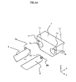
- FIG. 4A is an exploded view of light guides 1, 2 and holder 7 of the image sensor S1.
- FIG. 4B is an exploded view of light guides 1, 2 and holder 8 of the image sensor S1.
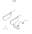
- FIG. 5A is an exploded view of light sources 3, 5, light-source board 11 and heat-transfer body 13 of the image sensor S1.
- FIG. 5B is an exploded view of light sources 4, 6, light-source board 12 and heat-transfer body 14 of the image sensor S1.
- FIG. 6 is an external view of the housing metal portion 110 for the image sensor S1.
- FIG. 7 is an expanded view of the housing metal portion 110 for the image sensor S1.
- FIG. 8 is a view of the housing 10 for the image sensor S 1 as seen from the irradiated side.
- FIG. 9 is a view of the housing 10 for the image sensor S 1 as seen from the rear surface.
- FIG. 10 is a side view of the image sensor S1.
- FIG. 11 is a cross-sectional view of line A-A in FIG. 10 .
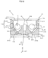
- FIG. 12 is a cross-sectional view of line B-B in FIG. 10 .
- FIG. 13 is a cross-sectional view of line C-C in FIG. 10 .
- FIG. 14A is a cross-sectional view of line D1-D1 in FIG. 10 .
- FIG. 14B is a cross-sectional view of line D2-D2 in FIG. 10 .
- FIG. 15A is a cross-sectional view of the main scanning direction of the holder 7 of the image sensor S1 (1/2).
- FIG. 15B is a cross-sectional view of the main scanning direction of the holder 8 of the image sensor S1 (2/2).
- the X-axis direction is the main scanning direction of the image sensor S1 (lengthwise direction of the image sensor S1).
- the Y-axis direction is the sub-scanning direction of the image sensor S1 (conveyance direction of the object being read and conveyed, short direction of the image sensor S1).
- the Z-axis direction is the focal depth direction of the image sensor S1 (thickness direction of the image sensor S1).
- the Z-axis direction is the optical axis direction of the rod lens array.
- the X axis, Y axis and Z axis are orthogonal to each other.
- the reading width direction of the image sensor S1 indicates the reading width (length of document being read) of only the main scanning direction of the image sensor S1.
- the image sensor S1 comprises: two light guides 1, 2 for irradiating the document; light sources 3, 4, 5, 6 that provide light for irradiating the light guides 1, 2; holders 7, 8 that hold the light guides 1, 2; a transparent-plate 9; a housing 10; light-source boards 11, 12; heat-transfer bodies 13, 14; a sensor 16; a sensor board 17; and reflecting plates 18, 19.
- the light guide 1 is formed using a transparent resin.
- the light guide 1 extends in the X-axis direction (main scanning direction).
- the light guide 1 is formed into a cylindrical shape with the X-axis direction being the lengthwise direction.
- the light guide 1 makes up the light emitter of a lighting device.
- the light guide 1 irradiates the document by guiding the light that is emitted by the light sources 3 and 4 in the X-axis direction and gradually releasing that light.
- the light guide 2 is arranged nearly parallel with the light guide 1.
- the light guide 2 is formed using a transparent resin.
- the light guide 2 is formed into a cylindrical shape with the X-axis direction (main scanning direction) being the lengthwise direction.
- the light guide 2 irradiates the document by guiding the light that is emitted by the light sources 5 and 6 in the X-axis direction and gradually releasing that light.
- the light guide 2 makes up the light emitter of a lighting device.
- the light guides 1, 2 are formed into a cylindrical shape with the X-axis direction being the lengthwise direction.
- the embodiment is not limited to this.
- the light guides 1, 2 could also be formed into a shape other than a cylindrical shape.
- the light source 3 projects light onto one end surface (end surface on the +X side) in the main scanning direction of the light guide 1.
- the light source 3 comprises a light-source element such as an LED light source.
- the light source 4 is located on the other end surface (end surface on the -X side) in the main scanning direction of the light guide 1.
- the light source 4 comprises a light-source element such as an LED light source.
- the light source 5 projects light onto one end surface (end surface on the +X side) in the main scanning direction of the light guide 2.
- the light source 5 comprises a light-source element such as an LED light source.
- the light source 6 is located on the other end surface (end surface on the -X side) in the scanning direction of the light guide 2.
- the light source 6 comprises a light-source element such as an LED light source.
- the holders 7 and 8 support the light guides 1, 2 and light sources 3 to 6.
- the end 1d on the +X side of the light guide 1, and the end 2d on the +X side of the light guide 2 are inserted into the holder 7.
- the light source 3 is located in the holder 7 facing the end surface on the +X side of the light guide 1.
- the light source 5 is located in the holder 7 facing the end surface on the +X side of the light guide 2.
- the end 1c on the -X side of the light guide 1, and the end 2c on the -X side of the light guide 2 are inserted into the holder 8.
- the light source 4 is located in the holder 8 facing the end surface on the -X side of the light guide 1.
- the light source 6 is located in the holder 8 facing the end surface on the -X side of the light guide 2.
- the transparent-plate 9 is formed using glass or a transparent resin. As illustrated in FIG. 1 and FIG. 2 , the transparent-plate 9 is located blocking the opening of the housing 10 so as to cover the lighting device or image sensor S1. An object being read such as a document or paper money is conveyed over this transparent-plate 9.
- the housing 10 is a frame that comprises an insert-molded body of metal and resin.
- the housing 10, as illustrated in FIG. 1 is such that stepped portions 10j, 10k that support the transparent-plate 9 are formed in the edge portion on the +Y and-Y sides of the opening of the housing 10.
- the stepped portions 10j, 10k are formed along the X-axis direction.
- the stepped sections of the stepped portions 10j, 10k are formed in a stepped shape in the Y direction (corresponds to the conveyance direction of the object being read).
- the transparent-plate 9 can be omitted.
- holes can be formed in the housing 10 for attaching the housing 10 to an image-reading device such as a copier or multi-function printer using screws, bolts or the like.
- the holes that are formed in the housing 10 can be formed on the outside (+X side) of the holder 7 and the outside (-X side) of the holder 8, and in both end sections in the Y direction of the housing 10.
- FIG. 3 is a constructional view of the image sensor S 1 of the first embodiment of the present disclosure as seen from the installed side of the sensor board 17.
- Gates 10m are formed in the housing 10 at two locations. The gates 10m are formed so as to protrude in the -Z direction. Holes 17a are formed in the sensor board 17 at two locations. The holes 17a pass through the sensor board 17 in the Z-axis direction. The gates 10m are inserted into the holes 17a. As a result, the sensor board 17 is attached to the housing 10.
- the gates 10m function as positioning pins for the sensor board 17.
- the sensor 16 is easily and accurately attached to an opening 211 that is provided in the housing 10. It is not illustrated in the drawings, however the sensor board 17 is fastened to the housing 10 with screws or the like.
- the holder 7 has an insertion hole 7a through which the light guide 1 is respectively inserted, and an insertion hole 7b through which the light guide 2 is respectively inserted.
- the insertion holes 7a, 7b pass through in the X-axis direction.
- Notches 7f, 7g are respectively formed in the inner-circumferential surfaces of the insertion holes 7a, 7b.
- Protrusions 1b, 2b that protrude in the radial direction are formed on the ends 1d, 2d on the +X sides of the light guides 1, 2.
- the notches 7f, 7g are formed into a shape capable of fitting with the protrusions 1b, 2b.
- the protrusions 1b, 2b By fitting the protrusions 1b, 2b into the notches 7f, 7h, the light guides 1, 2 are fastened to the holder 7 so as not to rotate around their respective axes.
- the protrusions 1b, 2b function as fittings that fit in the notches 7f, 7g.
- the holder 8 has insertion holes 8a, 8b through which the light guides 1, 2 are respectively inserted.
- Notches 8f, 8g are respectively formed in the openings of the insertion holes 8a, 8b.
- Protrusions 1a, 2a that protrude in the radial direction are formed on the ends 1c, 2c on the -X sides of the light guides 1, 2.
- the notches 8f, 8g are formed into a shape capable of fitting with the protrusions 1a, 2a.
- the light guides 1, 2 are fastened to the holder 7 so as not to rotate around their respective axes.
- the construction for fastening the light guides 1, 2 to the holder 7 is not limited to this.
- the insertion holes 7a, 7b can be formed in through holes that have a tapered shape in which the inner diameter gradually decreases in the +X direction.
- the light guides 1, 2 are fastened to the holder 7 by pressing the ends 1d, 2d of the light guides 1, 2 into the insertion holes 7a, 7b.
- the light guides 1, 2 are fastened to the holder 8 so as not to rotate around their respective axes.
- the construction for fastening the light guides 1, 2 to the holder 8 is not limited to this.
- the insertion holes 8a, 8b can be formed in through holes that have a tapered shape in which the inner diameter gradually decreases in the -X direction. In that case, the light guides 1, 2 are fastened to the holder 8 by pressing the ends 1c, 2c of the light guides 1, 2 into the insertion holes 8a, 8b.
- the insertion holes 7a, 7b should allow light to pass from the surface 7c to the surface 7d.
- the insertion holes 7a, 7b do not need to be penetrating holes. That is, there is no need for there to be empty space between the end surface of the light guide 1 and the light source 3.
- a transparent material that allows light to propagate can be filled into the insertion holes 7a, 7b that are through holes.
- the insertion holes 8a, 8b should allow light to pass from the surface 8c to the surface 8d.
- the insertion holes 8a, 8b do not need to be penetrating holes. That is, there is no need for there to be empty space between the end surface of the light guide 1 and the light source 4.
- a transparent material that allows light to propagate can be filled into the insertion holes 8a, 8b that are through holes.
- the light sources 3, 4 are respectively located at the end sections 1d, 1c on both sides of the light guide 1.
- the embodiment is not limited to this, and a light source could be located at only one end section of the end sections 1d, 1c.
- the light sources 5, 6 are respectively located at the end sections 2d, 2c on both sides of the light guide 2.
- the embodiment is not limited to this, and a light source could be located at only one end section of the end sections 2d, 2c.
- the light-source board 11 is a flexible board on which the light sources 3, 5 are mounted.
- the heat-transfer body 13 is arranged so as to come in contact with the surface opposite the surface where the light sources 3, 5 are mounted on the light-source board 11. By coming into contact with the light-source board 11, the heat-transfer body 13 transfers heat that is generated in the light-source board 11 to the housing metal portion 110.
- the light-source board 12 is a flexible board on which the light sources 4, 6 are mounted.
- the heat-transfer body 14 is arranged so as to come in contact with the surface opposite the surface where the light sources 4, 6 are mounted on the light-source board 12. By coming into contact with the light-source board 12, the heat-transfer body 14 transfers heat that is generated in the light-source board 12 to the housing metal portion 110.
- the reflection plate 18 extends in the X-axis direction (main scanning direction) and reflects light from the light guide 1.
- the reflection plate 18 is fastened to a reflection-plate-installation surface 10a of the housing 10.
- the reflection plate 19 extends in the X-axis direction and reflects light from the light guide 2.
- the reflection plate 19 is fastened to a reflection-plate-installation surface 10b (see FIG. 11 ) of the housing 10.
- the housing 10 is an insert-molded body of which a metal portion that is formed by bending metal plate is insert molded with resin.
- FIG. 6 is a constructional view of the housing metal portion 110
- FIG. 7 is an expanded view of this housing metal portion 110.
- the housing metal portion 110 of the housing 10 is formed by bending one sheet of sheet metal.
- FIG. 8 is a perspective view of the housing 10 as seen from the side on which the transparent-plate 9 is mounted
- FIG. 9 is a perspective view of the housing 10 as seen from the installation-surface side where the sensor board 17 is installed.
- the housing 10 comprises a housing metal portion 110 and a housing resin portion 210.
- FIG. 11 , FIG. 12 and FIG. 13 are cross-sectional views of line A-A, line B-B and line C-C in FIG. 10 .
- a lens 15 is an optical member or a combination of optical members that focuses reflected light that is emitted from the light guides 1, 2 and reflected by the object being read.
- the optical member is, for example, a lens array such as a rod lens array or macro lens array that focuses light onto a line sensor (sensor array).
- the lens 15 that is a combination of optical members, for example, is a lens or mirror of an image sensor (image reading device) of an optical reduction system.
- the sensor 16 is a sensor array that comprises sensor ICs that receive light that passes through the lens 15.
- the sensor board 17 is a circuit board on which the sensor 16 that is a light-receiving element is mounted.
- the sensor board 17 has a connector (not illustrated in the figures) that is capable of connecting with external devices.
- the sensor 16 receives light that was focused on the sensor 16 by the lens 15, and performs photoelectric conversion of that light.
- the length in the X-axis direction (main scanning direction) of the sensor 16 is a length that corresponds to the reading length of the image sensor S1.
- the connector outputs an electric signal that was obtained from the photoelectric conversion by the sensor 16 that is mounted on the sensor board 17 as an image signal to an external device of the sensor board 17.
- the sensor board 17 is fastened to the edge portion of the rear surface of the housing 10 by a fastening means such as screws.
- the transparent-plate 9 is located between the light guides 1, 2 and the object being read.
- the transparent-plate 9 prevents foreign matter from getting inside the housing 10.
- the transparent-plate 9 is made using a transparent material in order to suppress attenuating light that is irradiated from the light guides 1, 2 (line light source) and the light reflected from the object being read.
- FIG. 14A is a cross-sectional view of line D1-D1 in FIG. 10 .
- a holder fitting 20 for fitting the holder 7 inside is formed inside the housing 10.
- the holder fitting 20 is formed into a shape that corresponds to the shape of the holder 7. More specifically, the holder fitting 20 comprises positioning surfaces 10c, 10e, 10f.
- the bottom surface of the holder 7 that is fitted inside the holder fitting 20 comes in contact with the positioning surface 10c, which positions the holder 7 in the Z-axis direction. Moreover, the side surfaces on both sides of the holder 7 come in contact with the positioning surfaces 10e, 10f, which positions the holder 7 in the Y-axis direction.
- FIG. 14B is a cross-sectional view of line D2-D2 in FIG. 10 .
- a holder fitting 21 for fitting the holder 8 inside is formed inside the housing 10.
- the holder fitting 21 is formed into a shape that corresponds to the shape of the holder 8. More specifically, the holder fitting 21 comprises positioning surfaces 10d, 10g, 10h.
- the bottom surface of the holder 8 that is fitted inside the holder fitting 21 comes in contact with the positioning surface 10d, which positions the holder 8 in the Z-axis direction. Moreover, the side surfaces on both sides of the holder 8 come in contact with the positioning surfaces 10g, 10h, which positions the holder 8 in the Y-axis direction.
- FIG. 15A is a cross-sectional view in the main scanning direction of the holder 7 of the image sensor S1.
- the heat-transfer body 13 is arranged so as to come in contact with a heat-transfer-body-contact surface 10i of the housing metal portion 110. Heat that is generated by the light source 3 is transferred to the housing metal portion 110 by way of the heat-transfer-body-contact surface 10i.
- FIG. 15B is a cross-sectional view in the main scanning direction of the holder 8 of the image sensor S1.
- the heat-transfer body 14 is arranged so as to come in contact with a heat-transfer-body-contact surface 10i of the housing metal portion 110. Heat that is generated by the light source 4 is transferred to the housing metal portion 110 by way of the heat-transfer-body-contact surface 10i. As a result, it is possible to improve the heat dissipation of the image sensor S1.
- heat that is generated by the heat source 6 is also transferred to the housing metal portion 110 by way of the heat-transfer-body-contact surface 10i. As a result, it is possible to improve the heat dissipation of the image sensor S1.
- the housing 10 comprises a housing metal portion 110 and a housing resin portion 210.
- the housing metal portion 110 as illustrated in FIG. 6 and FIG. 7 , comprises a first bottom section 111, and a pair of sidewall sections 115 that are formed on both sides (+Y side and -Y side) of the first bottom section 111.
- a slit section 112 and first hole sections 116 are formed in the first bottom section 111.
- the slit section 112 is formed in order for reflected light that passed through the lens 15 to pass through.
- the slit section 112 is formed to have a specified opening width in the Y-axis direction (sub scanning direction).
- the slit section 112 extends in the X-axis direction (main scanning direction).
- the first hole sections 116 are through holes that pass through in the Z-axis direction.
- the first hole sections 116 are formed so as to be orthogonal to the slit section 112.
- the first hole sections 116 are intermittently formed at uniform intervals in the X-axis direction. As illustrated in FIG. 12 , the first hole sections 116 are formed at positions that correspond to reinforcing sections 213.
- the sidewall section 115 comprises a first sidewall 113 and a second sidewall 114.
- the first sidewall 113 is bent inward from the first bottom section 111 so as to incline at a specified angle.
- the first sidewall 113 extends in the X-axis direction (main scanning direction).
- the first sidewall 113 is formed such that the cross section is a circular arc shape.
- the second sidewall 114 is bent inward with respect to the first sidewall 113.
- the second sidewall 114 is orthogonal to the first bottom section 111.
- the second sidewall 114 extends in the X-axis direction (main scanning direction).
- second hole sections 117 are formed in the sidewall section 115.
- the second hole sections 117, as illustrated in FIG. 12 are formed at positions that correspond to holders 215.
- the housing resin portion 210 comprises a lens holder 212, reinforcing sections 213 that are formed on both sides (+Y side and -Y side) of the lens holder 212, a second bottom section 214, holders 215, and transparent-plate holders 216.
- the lens holder 212 comes in close contact with the slit section 112 of the housing metal portion 110.
- the lens holder 212 has an opening 211 having a width that is a little narrower than the width of the opening in the Y-axis direction (sub scanning direction) of the slit section 112. As illustrated in FIG. 8 , the lens holder 212 extends in the X-axis direction (main scanning direction). As illustrated in FIG. 11 to FIG. 13 , the lens 15 is fitted inside the opening 211 of the lens holder 212.
- the reinforcing sections 213, as illustrated in FIG. 12 reinforce the lens holder 212.
- the reinforcing sections 213 are integrally formed with the lens holder 212.
- the reinforcing sections 213 are formed so as to protrude upward from the first hole sections 116.
- a plurality of reinforcing sections 213 are formed.
- the reinforcing sections 213 are provided so as to be separated at uniform intervals along the X-axis direction (main scanning direction).
- the second bottom section 214 is integrally formed with the reinforcing sections 213 by way of the first hole sections 116.
- the second bottom section 214 as illustrated in FIG. 9 , has a plurality of sensor-board holders 214a.
- the sensor-board holders 214a are provided so as to be separated at uniform intervals along the X-axis direction (main scanning direction).
- the holders 215 are integrally formed with the second bottom section 214.
- the holders 215 are formed between the second bottom section 214 and the first sidewall 113.
- the holders 215 are provided at positions that face the reinforcing sections 213.
- the holders 215 hold the second bottom section 214.
- the transparent-plate holders 216 as illustrated in FIG. 11 to FIG. 13 are continuously formed from all of the holders 215 by way of the second hole sections 117.
- the transparent-plate holders 216 come in close contact with the inside and end sections of the second sidewall 114.
- the transparent-plate holders 216 extend in the main scanning direction.
- the transparent-plate 9 is placed on the housing edge on the top ends of the transparent-plate holders 216. More specifically, the transparent-plate 9 is fitted in the stepped portions 10j, 10k of the housing 10.
- the housing resin portion 210 is divided into three components; the transparent-plate holders 216, the second bottom section 214. and the lens holder 212.
- the transparent-plate holders 216 can adjust the position of the transparent-plate 9 that determines the focal position in order to hold the transparent-plate 9.
- the lens holder 212 holds the lens 15, so can adjust the position of the lens 15.
- each of these three components are caused to curve in the concave direction with respect to the surface that comes in contact with the housing metal portion 110.
- the housing resin portion 210 is divided into three portions, however, as illustrated in FIG. 12 , in the cross section of line B-B of the housing 10, the housing resin portion 210 is integrated into one in the YZ plane.
- the lens holder 212, the reinforcing sections 213, the second bottom section 214, the holders 215, and the transparent-plate holders 216 are integrated into one by way of the first hole sections 116 and second hole sections 117.
- the housing resin portion 210 that is divided in cross section of line A-A of the housing 10 is integrated into one in the cross section of line B-B of the housing 10, so it is possible to improve the flow of resin during insert molding, and molding can be performed stably at low injection pressure. As a result, it is possible to improve the precision of the relative positions of the object being read that is placed on the transparent-plate 9, the sensor 16 and the lens 15.
- the housing resin portion 210 has two components; the transparent-plate holders 216 and the lens holder 212.
- the sensor-board holders 214a are provided so as to be separated at uniform intervals in the X-axis direction (main scanning direction).
- the linear expansion coefficients of the housing resin portion 210 and the housing metal portion 110 are different, it is possible to reduce the stress that occurs when the temperature changes. Consequently, it is possible to form a housing 10 that is capable of handling well changes in temperature. Moreover, it is possible to improve the precision of the relative positions of the object being read that is placed on the transparent-plate 9, the sensor 16, and the lens 15.
- the lens holder 212 is formed so as to pass through the slit section 112 and continues until it reaches the sensor board 17. Therefore, it is possible to prevent divergence of the optical axis and to suppress stray light.
- the housing 10 comprises a housing metal portion 110 and housing resin portion 210 that are integrally formed.
- an image sensor S1 is obtained having a housing 10 that has good heat dissipation, suppresses distortion, and has a highly precise shape.
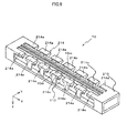
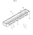
- FIG. 16 is a perspective view of the housing 10A of the image sensor S2 of the second embodiment as seen from the irradiated side.
- FIG. 17 is a perspective view of the housing 10A of the image sensor S2 of the second embodiment as seen from the rear surface.
- FIG. 18 is a side view of the image sensor S2 of the second embodiment.
- the image sensor S2 of the second embodiment differs from the image sensor S 1 of the first embodiment in that the construction of the housing 10A differs from that of the housing 10 explained in the first embodiment.
- the housing 10A as illustrated in FIG. 16 and FIG. 17 , is formed into a rectangular parallelepiped shape with the lengthwise direction being the X-axis direction (main scanning direction).
- the housing 10A comprises a housing metal portion 110 and a housing resin portion 210.
- the housing 10A is an insert-molded body that is formed by insert molding of the housing resin portion 210 in the housing metal portion 110.
- FIG. 19 is a cross-sectional view of line E-E in FIG. 18 .
- FIG. 20 is a cross-sectional view of line F-F in FIG. 18 .
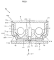
- FIG. 21 is a cross-sectional view of line G-G in FIG. 18 .
- the housing metal portion 110 is formed into a U shape in the YZ cross section.
- the housing metal portion 110 comprises a first bottom section 111 in the center of the U shape, and sidewall sections 115 that are formed on the both sides (+Y side and -Y side) of the first bottom section 111.
- the first bottom section 111 is formed so as to extend in the X-axis direction (main scanning direction).
- a slit section 112 is formed in the first bottom section 111.
- the slit section 112 is formed so as to extend in the X-axis direction.
- openings 118 are formed in the first bottom section 111 so as to pass through in the Y-axis direction.
- the openings 118 are formed so as to have a circular cross section. In the second embodiment, two openings 118 are formed.
- each sidewall section 115 is bent toward the top side (+Z side) from both ends of the first bottom section 111.
- Each sidewall section 115 comprises a first sidewall 113 and a second sidewall 114.
- the sidewall sections 115 are formed so as to extend in the X-axis direction.
- the first sidewall 113 is formed into a wave shape that curves such that the YZ cross section is uneven. More specifically, the first sidewall 113 is formed into a wave shape that has a convex section 113a that is convex toward the inside.
- the second sidewall 114 is formed so as to be orthogonal to the first bottom section 111.
- the housing resin portion 210 comprises a lens holder 212, reinforcing sections 213 on both sides (+Y side and -Y side) of the lens holder 212, reflection-plate-installation sections 218, transparent-plate holders 216, a second bottom section 214 and gates 217.
- the lens holder 212 comes in close contact with the slit section 112 of the housing metal portion 110.
- the lens holder 212 is formed so as to protrude toward the top side (+Z side) from the second bottoms section 214.
- the lens holder 212 as illustrated in FIG. 16 , is formed so as to linearly extend in the X-axis direction.
- An opening 211 is formed along the X-axis direction in this lens holder 212.
- the opening 211 is formed such that opening width is smaller than the opening width (opening width in the Y-axis direction) of the slit section 112 of the housing metal portion 110.
- the opening 211 is a through hole that passes through in the Z-axis direction.
- the lens 15 is fitted inside this opening 211 from the top side.
- the reinforcing sections 213 are formed near the bottom end of the lens holder 212.
- the reinforcing sections 213 are formed so as to linearly extend in the X-axis direction along the lens holder 212.
- the reinforcing sections 213 are formed for maintaining the strength of the lens holder 212.
- the reflection-plate-installation sections 218 are formed so as to be continuous with the reinforcing sections 213.
- the reflection-plate-installation sections 218 are formed on the inside of the sidewall sections 115.
- the surfaces of the reflection-plate-installation sections 218 are formed as inclined surfaces that are inclined with respect to the XY plane. Reflection plates 18, 19 are installed on the reflection-plate-installation sections 218.
- the reflection plates 18, 19 were installed on reflection-plate-installation surfaces 10a, 10b, which were part of the housing metal portion 110.
- the reflection plates 18, 19 are installed on the reflection-plate-installation sections 218, which are part of the housing resin portion 210.
- the transparent-plate holders 216 are formed so as to be continuous with the reflection-plate-installation sections 218.
- the transparent-plate holders 216 come in close contact with the inside and end sections of the second sidewalls 114.
- the transparent-plate holders 216 extend in the main scanning direction.
- the transparent-plate 9 is placed on the housing edge sections on the top ends of the transparent-plate holders 216. More specifically, the transparent-plate 9 is fitted in the stepped portions 10j, 10k of the housing 10.
- the second bottom section 214 covers the first bottom section 111 of the housing metal portion 110 with part exposed.
- the sensor board 17 is attached to and supported by the bottom surface (surface on the -Z side) of the second bottom section 214.
- the sensor board 17, for example, is fastened by a fastening means such as screws.
- the second bottom section 214 also has a plurality of sensor-board holders 214a.
- the sensor-board holders 214a are provided so as to be separated at uniform intervals along the X-axis direction (main scanning direction).
- the gates 217 are formed so as to protrude from the bottom surface of the second bottom section 214.
- the gates 217 are formed into a circular column shape. In this embodiment, two gates 217 are formed.
- the gates 217 are formed so that the center axes thereof respectively coincide with the center axes of the openings 118 that is formed in the first bottom section 111 of the housing metal portion 110.
- the gates 217 are also formed so that the outer diameters thereof are the same as the inner diameters of the openings 118.
- the gates 217 are inserted into holes 17a in the sensor board 17.
- the tip-end sections of the gates 217 are exposed from the bottom surface of the sensor board 17.
- the housing metal portion 110 and the housing resin portion 210 are integrally formed.
- an image sensor S2 is obtained that has a housing 10A that has good heat dissipation, suppresses distortion, and has a highly precise shape.
- the housing resin portion 210 comprises the transparent-plate holders 216, the sensor-board holders 214a, and the lens holder 212. Therefore, it is possible to adjust the transparent-plate 9, sensor 16 and lens 15 by each of components at three locations, or in other words, by the transparent-plate holders 216, the sensor-board holders 214a, and the lens holder 212, and thus it is possible to improve the precision of the relative positions of the object being read that is placed on the transparent-plate 9, the sensor 16 and the lens 15.
- each of these three components is caused to bend in a concave direction with respect to the respective surfaces that come in contact with the housing metal portion 110. Therefore, by adjusting the contact surface area of these three components and the housing metal portion 110, it is possible to adjust the amount of deformation in the X and Z directions of the housing 10A. Consequently, it is possible to suppress bending in the main scanning direction in the housing 10A.
- openings 118 are formed in the housing metal portion 110 of the housing 10A.
- the openings 118 are formed such that the center axes thereof coincide with the center axes of the gates 217.
- the molten resin R that is injected from the resin injection opening 301 preferentially flows as indicated by the arrows A through the openings 118.
- the molten resin R that is injected from the resin injection openings 301 of the molding die 300 flows as illustrated by arrow A or arrow B in FIG. 22B into an inside cavities 302A that are formed on the inside of the housing metal portion 110 or outside cavities 302B that are formed on the outside.
- the openings 118 are formed so that the center axes respectively coincide with the center axes of the gates 217, so the amount of molten resin R that is flowing in the direction of arrow A is greater than the amount of molten resin R that is flowing in the direction of arrow B.
- the space C between the sidewall sections 115 of the housing metal portion 110 and the molding die 300 becomes small. This makes it possible to form the housing 10A having highly precise dimensions regardless of differences in the dimensions of the housing metal portion 110 that is molded. As a result, an image sensor S2 having a housing 10A with a highly precise shape can be obtained.
- the space C between the sidewall sections 115 of the housing metal portion 110 and the molding die 300 becomes small, so it is possible to suppress the occurrence of burrs due to the space C. Therefore, it is possible to form a housing 10A having highly precise dimensions. As a result, an image sensor S2 having a housing 10A with a highly precise shape can be obtained.
- the first sidewalls 113 of the sidewall sections 115 of the housing metal portion 110 are such that the YZ cross section is formed into a wave shape that is curved in an irregular shape. Therefore, it is difficult for twisting or bending to occur in the housing metal portion 110. Consequently, it is possible to improve the rigidity of the housing 10A. As a result, an image sensor S2 having a housing 10A with a highly precise shape can be obtained.
- the housing resin portion 210 comprises reinforcing sections 213 that reinforce the lens holder 212. Therefore, it is possible to improve the strength of the lens holder 212, and it is possible to improve the precision of the relative positions of the object being read that is placed on the transparent-plate 9, the sensor 16 and the lens 15.
- convex sections 113a that are convex toward the inside are formed on the first sidewalls 113. Therefore, it is possible to make the thickness of the resin near the reflection-plate-installation sections 218 thin. As a result, it is possible to suppress shrinkage that occurs during insert molding. Therefore, it is possible to form a housing 10A having highly precise dimensions. As a result, an image sensor S2 having a housing 10A with a highly precise shape can be obtained.
- the sensor-board holders 214a are provided so as to be separated at specified intervals along the X-axis direction. Therefore, it is possible to reduce the stress that is generated during temperature changes due to differences in the linear expansion coefficients of the housing resin portion 210 and housing metal portion 110. As a result, an image sensor S2 having a housing 10A with a highly precise shape can be obtained.
- the openings 118 that are formed in the housing metal portion 110 are formed so that the center axes coincide with the center axes of the gates 217.
- the embodiments are not limited to this, the openings 118 and gates 217 only need to be overlapped on the same axis.
- the molten resin R that is injected from the resin injection opening 301 preferentially flows in the direction indicated by arrow A.
- the image sensor of the present disclosure is suitable for use in an image reading device such as a copier or multi-function printer, and is suitable for reading a target object.
Landscapes
- Engineering & Computer Science (AREA)
- Multimedia (AREA)
- Signal Processing (AREA)
- Physics & Mathematics (AREA)
- Optics & Photonics (AREA)
- Facsimile Heads (AREA)
- Facsimile Scanning Arrangements (AREA)
Abstract
Description
- The present disclosure relates to an image sensor that is used in an image reading device such as a copier or a multi-function printer.
- Contact image sensors that are used in image reading devices such as copiers or multi-function printers are advancing in terms of increased precision of reading depth and higher resolution. Therefore, in an optical system for a contact image sensor, construction is desired in which the relative positional relationship of a document, a lens and sensor is regulated with high precision.
- Unexamined Japanese Patent Application Kokai Publication
JP H07-131 585 - Moreover, in the optical system of a contact image sensor, light that is reflected from the document, passes through a lens and reaches the sensor, is converted by the sensor to an electrical signal so that information in the document is converted to the electrical signal. However, when there is divergence of the optical axis, irregular reflection of light occurs by the light that passes through the lens hitting a location other than the sensor, and that light arrives at the sensor as stray light, causing the image reading performance to become poor.
- Unexamined Japanese Patent Application Kokai Publication
JP H08-307 597 A - As the light output from light sources of contact image sensors becomes greater, there is a need for efficient heat-dissipating construction. Unexamined Japanese Patent Application Kokai Publication
JP 2008-227 815 A FIG. 4 , heat-dissipating construction in which an LED chip is mounted on a metal plate, and bent heat-dissipating plates are attached to a flat section on the reflecting-surface side of the LED chip. -
- Patent Literature 1:
- Unexamined Japanese Patent Application Kokai Publication
JP H07-131 585 A - Patent Literature 2:
- Unexamined Japanese Patent Application Kokai Publication
JP H08-307 597 A - Patent Literature 3:
- Unexamined Japanese Patent Application Kokai Publication
JP 2008-227 815 A - However, in the device disclosed in
Patent Literature 1, one of the document glass or sensor-mounted board is fastened to a high-precision member, however, the other is fastened to a resin member, which is a separate part. Therefore, the relative position of the document glass and the sensor-mounted board is affected by differences in the dimensions of the high-precision member and the resin member, and as a result, there is a problem in that the precision of the relative positions of the rod lens, document glass and sensor-mounted board is low. - In the case of the contact-type image sensor disclosed in
Patent Literature 2, in addition to the frame, a separate holder for preventing light rays that are irradiated by the LED chip from directly entering into the light-receiving sensor, and that holds the rod lens array is necessary, and as a result, there is a problem in that construction is complicated. As the construction becomes complicated, it becomes difficult to form a housing having high precision. - The contact image sensor that is disclosed in
Patent Literature 3 has heat-dissipating plates and plate springs for securing the heat-dissipating plates, so construction is complicated. When the construction is complicated, it becomes difficult to form a housing having high precision. - The object of the present disclosure is to obtain an image sensor that eliminates the problems described above, and that has a housing having a highly precise shape.
- The image sensor of this disclosure comprises a light guide that extends in a main scanning direction and that emits light onto an irradiated body; a lens that focuses reflected light that has been reflected by the irradiated body; a light receiver that receives the reflected light that was focused by the lens; and a housing. The housing houses or holds the light guide, the lens, and the light receiver, and comprises a metal portion and a resin portion that are formed into one housing.
- With this disclosure, the housing is formed by integrating a metal portion and a resin portion, so an image sensor is obtained that uses a housing that has good heat dissipation, suppresses distortion and has a highly precise shape.
-
- FIG. 1
- is an exploded view of an image sensor of a first embodiment of the present disclosure;
- FIG. 2
- is a perspective view of the image sensor of the first embodiment of the present disclosure;
- FIG. 3
- is a constructional view of the image sensor of the first embodiment of the present disclosure as seen from the installed side of a sensor board;
- FIG. 4A
- is an exploded view of light guides and holder of the image sensor (lighting device) of the first embodiment of the present disclosure (1/2);
- FIG. 4B
- is an exploded view of light guides and holder of the image sensor (lighting device) of the first embodiment of the present disclosure (2/2);
- FIG. 5A
- is an exploded view of light sources, light-source board and heat-transfer body of the image sensor of the first embodiment of the present disclosure (1/2);
- FIG. 5B
- is an exploded view of light sources, light-source board and heat-transfer body of the image sensor of the first embodiment of the present disclosure (2/2);
- FIG. 6
- is an external view of a housing metal portion for the image sensor of the first embodiment of the present disclosure;
- FIG. 7
- is an expanded view of the housing metal portion for the image sensor of the first embodiment of the present disclosure;
- FIG. 8
- is a view of a housing for the image sensor of the first embodiment of the present disclosure as seen from the irradiated side;
- FIG. 9
- is a view of the housing for the image sensor of the first embodiment of the present disclosure as seen from the rear surface;
- FIG. 10
- is a side view of the image sensor of the first embodiment of the present disclosure;
- FIG. 11
- is a cross-sectional view of line A-A in
FIG. 10 ; - FIG. 12
- is a cross-sectional view of line B-B in
FIG. 10 ; - FIG. 13
- is a cross-sectional view of line C-C in
FIG. 10 ; - FIG. 14A
- is a cross-sectional view of line D1-D1 in
FIG. 10 ; - FIG. 14B
- is a cross-sectional view of line D2-D2 in
FIG. 10 ; - FIG. 15A
- is a cross-sectional view of the main scanning direction of the holder of the image sensor of the first embodiment of the present disclosure (1/2);
- FIG. 15B
- is a cross-sectional view of the main scanning direction of the holder of the image sensor of the first embodiment of the present disclosure (2/2);
- FIG. 16
- is a view of the housing of the image sensor of a second embodiment of the present disclosure as seen from the irradiated side;
- FIG. 17
- is a view of the housing of the image sensor of the second embodiment of the present disclosure as seen from the rear surface;
- FIG. 18
- is a side view of the image sensor of the second embodiment of the present disclosure;
- FIG. 19
- is a cross-sectional view of line E-E in
FIG. 18 ; - FIG. 20
- is a cross-sectional view of line F-F in
FIG. 18 ; - FIG. 21
- is a cross-sectional view of line G-G in
FIG. 18 ; - FIG. 22A
- is a cross-sectional view for explaining the application of the image sensor of the second embodiment of the present disclosure (1/2); and
- FIG. 22B
- is a cross-sectional view for explaining the application of the image sensor of the second embodiment of the present disclosure (2/2).
- In the following, an image sensor S1 of a first embodiment of the present disclosure will be explained using
FIG. 1 to FIG. 15B .FIG. 1 is an exploded view of theimage sensor S 1 of this first embodiment of the present disclosure.FIG. 2 is a perspective view of the image sensor S1.FIG. 3 is a constructional view of the image sensor S1 as seen from the installed side of thesensor board 17.FIG. 4A is an exploded view of light guides 1, 2 andholder 7 of the image sensor S1.FIG. 4B is an exploded view of light guides 1, 2 andholder 8 of the image sensor S1. -
FIG. 5A is an exploded view oflight sources source board 11 and heat-transfer body 13 of the image sensor S1.FIG. 5B is an exploded view oflight sources 4, 6, light-source board 12 and heat-transfer body 14 of the image sensor S1.FIG. 6 is an external view of thehousing metal portion 110 for the image sensor S1.FIG. 7 is an expanded view of thehousing metal portion 110 for the image sensor S1. -
FIG. 8 is a view of thehousing 10 for theimage sensor S 1 as seen from the irradiated side.FIG. 9 is a view of thehousing 10 for theimage sensor S 1 as seen from the rear surface.FIG. 10 is a side view of the image sensor S1.FIG. 11 is a cross-sectional view of line A-A inFIG. 10 .FIG. 12 is a cross-sectional view of line B-B inFIG. 10 . -
FIG. 13 is a cross-sectional view of line C-C inFIG. 10 .FIG. 14A is a cross-sectional view of line D1-D1 inFIG. 10 .FIG. 14B is a cross-sectional view of line D2-D2 inFIG. 10 .FIG. 15A is a cross-sectional view of the main scanning direction of theholder 7 of the image sensor S1 (1/2).FIG. 15B is a cross-sectional view of the main scanning direction of theholder 8 of the image sensor S1 (2/2). - The Z-axis direction is the focal depth direction of the image sensor S1 (thickness direction of the image sensor S1). When the image sensor S1 is a contact image sensor, the Z-axis direction is the optical axis direction of the rod lens array. The X axis, Y axis and Z axis are orthogonal to each other.
- In the first embodiment of the present disclosure, the reading width direction of the image sensor S1 indicates the reading width (length of document being read) of only the main scanning direction of the image sensor S1.
- As illustrated in
FIG. 1 , the image sensor S1 comprises: twolight guides light sources holders plate 9; ahousing 10; light-source boards transfer bodies sensor 16; asensor board 17; and reflectingplates - The
light guide 1 is formed using a transparent resin. Thelight guide 1 extends in the X-axis direction (main scanning direction). Thelight guide 1 is formed into a cylindrical shape with the X-axis direction being the lengthwise direction. Thelight guide 1 makes up the light emitter of a lighting device. Thelight guide 1 irradiates the document by guiding the light that is emitted by thelight sources - The
light guide 2 is arranged nearly parallel with thelight guide 1. Thelight guide 2 is formed using a transparent resin. Thelight guide 2 is formed into a cylindrical shape with the X-axis direction (main scanning direction) being the lengthwise direction. Thelight guide 2 irradiates the document by guiding the light that is emitted by thelight sources 5 and 6 in the X-axis direction and gradually releasing that light. Thelight guide 2 makes up the light emitter of a lighting device. - In the first embodiment, the light guides 1, 2 are formed into a cylindrical shape with the X-axis direction being the lengthwise direction. However, the embodiment is not limited to this. The light guides 1, 2 could also be formed into a shape other than a cylindrical shape.
- The
light source 3 projects light onto one end surface (end surface on the +X side) in the main scanning direction of thelight guide 1. Thelight source 3 comprises a light-source element such as an LED light source. Thelight source 4 is located on the other end surface (end surface on the -X side) in the main scanning direction of thelight guide 1. Thelight source 4 comprises a light-source element such as an LED light source. - The
light source 5 projects light onto one end surface (end surface on the +X side) in the main scanning direction of thelight guide 2. Thelight source 5 comprises a light-source element such as an LED light source. The light source 6 is located on the other end surface (end surface on the -X side) in the scanning direction of thelight guide 2. The light source 6 comprises a light-source element such as an LED light source. - The
holders light sources 3 to 6. - In
FIG. 1 , theend 1d on the +X side of thelight guide 1, and theend 2d on the +X side of thelight guide 2 are inserted into theholder 7. Moreover, thelight source 3 is located in theholder 7 facing the end surface on the +X side of thelight guide 1. Thelight source 5 is located in theholder 7 facing the end surface on the +X side of thelight guide 2. - The
end 1c on the -X side of thelight guide 1, and theend 2c on the -X side of thelight guide 2 are inserted into theholder 8. Moreover, thelight source 4 is located in theholder 8 facing the end surface on the -X side of thelight guide 1. The light source 6 is located in theholder 8 facing the end surface on the -X side of thelight guide 2. - The transparent-
plate 9 is formed using glass or a transparent resin. As illustrated inFIG. 1 andFIG. 2 , the transparent-plate 9 is located blocking the opening of thehousing 10 so as to cover the lighting device or image sensor S1. An object being read such as a document or paper money is conveyed over this transparent-plate 9. - The
housing 10 is a frame that comprises an insert-molded body of metal and resin. Thehousing 10, as illustrated inFIG. 1 , is such that steppedportions plate 9 are formed in the edge portion on the +Y and-Y sides of the opening of thehousing 10. The steppedportions portions - When a transparent plate equivalent to transparent-
plate 9 is already equipped in an image-reading device such as a copier or multi-function printer or the like in which the image sensor S1 is mounted, the transparent-plate 9 can be omitted. Furthermore, holes can be formed in thehousing 10 for attaching thehousing 10 to an image-reading device such as a copier or multi-function printer using screws, bolts or the like. For example, the holes that are formed in thehousing 10 can be formed on the outside (+X side) of theholder 7 and the outside (-X side) of theholder 8, and in both end sections in the Y direction of thehousing 10. -
FIG. 3 is a constructional view of theimage sensor S 1 of the first embodiment of the present disclosure as seen from the installed side of thesensor board 17.Gates 10m are formed in thehousing 10 at two locations. Thegates 10m are formed so as to protrude in the -Z direction.Holes 17a are formed in thesensor board 17 at two locations. Theholes 17a pass through thesensor board 17 in the Z-axis direction. Thegates 10m are inserted into theholes 17a. As a result, thesensor board 17 is attached to thehousing 10. - In other words, the
gates 10m function as positioning pins for thesensor board 17. In this way, thesensor 16 is easily and accurately attached to anopening 211 that is provided in thehousing 10. It is not illustrated in the drawings, however thesensor board 17 is fastened to thehousing 10 with screws or the like. - In
FIG. 4A , theholder 7 has aninsertion hole 7a through which thelight guide 1 is respectively inserted, and aninsertion hole 7b through which thelight guide 2 is respectively inserted. The insertion holes 7a, 7b pass through in the X-axis direction.Notches insertion holes -
Protrusions ends notches protrusions protrusions notches 7f, 7h, the light guides 1, 2 are fastened to theholder 7 so as not to rotate around their respective axes. In other words, theprotrusions notches - In
FIG. 4B , theholder 8 hasinsertion holes Notches insertion holes Protrusions 1a, 2a that protrude in the radial direction are formed on theends notches protrusions 1a, 2a. By fitting theprotrusions 1a, 2a into thenotches 8f, 8h, the light guides 1, 2 are fastened to theholder 8 so as not to rotate around their respective axes. In other words, theprotrusions 1a, 2a function as fittings. - As illustrated in
FIG. 4A , in the first embodiment, by fitting theprotrusions notches holder 7 so as not to rotate around their respective axes. However, the construction for fastening the light guides 1, 2 to theholder 7 is not limited to this. - For example, the
insertion holes holder 7 by pressing theends insertion holes - Similarly, as illustrated in
FIG. 4B , in the first embodiment, by fitting theprotrusions 1a, 2a in thenotches holder 8 so as not to rotate around their respective axes. However, the construction for fastening the light guides 1, 2 to theholder 8 is not limited to this. For example, theinsertion holes holder 8 by pressing theends insertion holes - As illustrated in
FIG. 4A , theinsertion holes surface 7c to thesurface 7d. In other words, as long as light from thelight sources insertion holes light guide 1 and thelight source 3. - Similarly, there is no need for there to be empty space between the end surface of the
light guide 2 and thelight source 5. Moreover, a transparent material that allows light to propagate can be filled into theinsertion holes - As illustrated in
FIG. 4B , theinsertion holes surface 8c to thesurface 8d. In other words, as long as light from thelight sources 4, 6 can propagate along the light guides 1, 2, theinsertion holes light guide 1 and thelight source 4. - Similarly, there is no need for there to be empty space between the end surface of the
light guide 2 and the light source 6. Moreover, a transparent material that allows light to propagate can be filled into theinsertion holes - As illustrated in
FIG. 1 , thelight sources end sections light guide 1. However, the embodiment is not limited to this, and a light source could be located at only one end section of theend sections light sources 5, 6 are respectively located at theend sections light guide 2. However, the embodiment is not limited to this, and a light source could be located at only one end section of theend sections - In
FIG. 5A , the light-source board 11 is a flexible board on which thelight sources transfer body 13 is arranged so as to come in contact with the surface opposite the surface where thelight sources source board 11. By coming into contact with the light-source board 11, the heat-transfer body 13 transfers heat that is generated in the light-source board 11 to thehousing metal portion 110. - In
FIG. 5B , the light-source board 12 is a flexible board on which thelight sources 4, 6 are mounted. The heat-transfer body 14 is arranged so as to come in contact with the surface opposite the surface where thelight sources 4, 6 are mounted on the light-source board 12. By coming into contact with the light-source board 12, the heat-transfer body 14 transfers heat that is generated in the light-source board 12 to thehousing metal portion 110. - In
FIG. 1 , thereflection plate 18 extends in the X-axis direction (main scanning direction) and reflects light from thelight guide 1. Thereflection plate 18 is fastened to a reflection-plate-installation surface 10a of thehousing 10. - The
reflection plate 19 extends in the X-axis direction and reflects light from thelight guide 2. Thereflection plate 19 is fastened to a reflection-plate-installation surface 10b (seeFIG. 11 ) of thehousing 10. - The
housing 10 is an insert-molded body of which a metal portion that is formed by bending metal plate is insert molded with resin.FIG. 6 is a constructional view of thehousing metal portion 110, andFIG. 7 is an expanded view of thishousing metal portion 110. Thehousing metal portion 110 of thehousing 10 is formed by bending one sheet of sheet metal. -
FIG. 8 is a perspective view of thehousing 10 as seen from the side on which the transparent-plate 9 is mounted, andFIG. 9 is a perspective view of thehousing 10 as seen from the installation-surface side where thesensor board 17 is installed. Thehousing 10 comprises ahousing metal portion 110 and ahousing resin portion 210. -
FIG. 11 ,FIG. 12 andFIG. 13 are cross-sectional views of line A-A, line B-B and line C-C inFIG. 10 . - In
FIG. 1 , andFIG. 11 toFIG. 13 , alens 15 is an optical member or a combination of optical members that focuses reflected light that is emitted from the light guides 1, 2 and reflected by the object being read. When the image sensor S1 is a reflected light source type of sensor, the optical member is, for example, a lens array such as a rod lens array or macro lens array that focuses light onto a line sensor (sensor array). - The
lens 15 that is a combination of optical members, for example, is a lens or mirror of an image sensor (image reading device) of an optical reduction system. Thesensor 16 is a sensor array that comprises sensor ICs that receive light that passes through thelens 15. - In
FIG. 1 ,FIG. 3 andFIG. 11 toFIG. 13 , thesensor board 17 is a circuit board on which thesensor 16 that is a light-receiving element is mounted. Thesensor board 17 has a connector (not illustrated in the figures) that is capable of connecting with external devices. Moreover, thesensor 16 receives light that was focused on thesensor 16 by thelens 15, and performs photoelectric conversion of that light. The length in the X-axis direction (main scanning direction) of thesensor 16 is a length that corresponds to the reading length of the image sensor S1. - The connector outputs an electric signal that was obtained from the photoelectric conversion by the
sensor 16 that is mounted on thesensor board 17 as an image signal to an external device of thesensor board 17. Thesensor board 17 is fastened to the edge portion of the rear surface of thehousing 10 by a fastening means such as screws. - In
FIG. 1 , andFIG. 11 toFIG. 13 , the transparent-plate 9 is located between the light guides 1, 2 and the object being read. The transparent-plate 9 prevents foreign matter from getting inside thehousing 10. The transparent-plate 9 is made using a transparent material in order to suppress attenuating light that is irradiated from the light guides 1, 2 (line light source) and the light reflected from the object being read. -
FIG. 14A is a cross-sectional view of line D1-D1 inFIG. 10 . InFIG. 14A , a holder fitting 20 for fitting theholder 7 inside is formed inside thehousing 10. The holder fitting 20 is formed into a shape that corresponds to the shape of theholder 7. More specifically, the holder fitting 20 comprisespositioning surfaces 10c, 10e, 10f. - The bottom surface of the
holder 7 that is fitted inside the holder fitting 20 comes in contact with thepositioning surface 10c, which positions theholder 7 in the Z-axis direction. Moreover, the side surfaces on both sides of theholder 7 come in contact with the positioning surfaces 10e, 10f, which positions theholder 7 in the Y-axis direction. -
FIG. 14B is a cross-sectional view of line D2-D2 inFIG. 10 . InFIG. 14B , a holder fitting 21 for fitting theholder 8 inside is formed inside thehousing 10. The holder fitting 21 is formed into a shape that corresponds to the shape of theholder 8. More specifically, the holder fitting 21 comprisespositioning surfaces - The bottom surface of the
holder 8 that is fitted inside the holder fitting 21 comes in contact with thepositioning surface 10d, which positions theholder 8 in the Z-axis direction. Moreover, the side surfaces on both sides of theholder 8 come in contact with the positioning surfaces 10g, 10h, which positions theholder 8 in the Y-axis direction. - By fitting the
holders holder fittings housing 10, it is possible to align the center in the Y direction of theholders 7, 8 (in other words, the center of lighting) with the optical axis. -
FIG. 15A is a cross-sectional view in the main scanning direction of theholder 7 of the image sensor S1. InFIG. 15A , the heat-transfer body 13 is arranged so as to come in contact with a heat-transfer-body-contact surface 10i of thehousing metal portion 110. Heat that is generated by thelight source 3 is transferred to thehousing metal portion 110 by way of the heat-transfer-body-contact surface 10i. - As a result, it is possible to improve the heat dissipation of the image sensor S1. Similarly, as can be seen by referencing
FIG. 15A andFIG. 5A , heat that is generated by theheat source 5 is also transferred to thehousing metal portion 110 by way of the heat-transfer-body-contact surface 10i. As a result, it is possible to improve the heat dissipation of the image sensor S1. -
FIG. 15B is a cross-sectional view in the main scanning direction of theholder 8 of the image sensor S1. InFIG. 15B , the heat-transfer body 14 is arranged so as to come in contact with a heat-transfer-body-contact surface 10i of thehousing metal portion 110. Heat that is generated by thelight source 4 is transferred to thehousing metal portion 110 by way of the heat-transfer-body-contact surface 10i. As a result, it is possible to improve the heat dissipation of the image sensor S1. - Similarly, as can be seen by referencing
FIG. 15B andFIG. 5B , heat that is generated by the heat source 6 is also transferred to thehousing metal portion 110 by way of the heat-transfer-body-contact surface 10i. As a result, it is possible to improve the heat dissipation of the image sensor S1. - In
FIG. 8 ,FIG. 9 andFIG. 11 toFIG. 13 , thehousing 10 comprises ahousing metal portion 110 and ahousing resin portion 210. - The
housing metal portion 110, as illustrated inFIG. 6 andFIG. 7 , comprises afirst bottom section 111, and a pair ofsidewall sections 115 that are formed on both sides (+Y side and -Y side) of thefirst bottom section 111. - A
slit section 112 andfirst hole sections 116 are formed in thefirst bottom section 111. Theslit section 112 is formed in order for reflected light that passed through thelens 15 to pass through. Theslit section 112 is formed to have a specified opening width in the Y-axis direction (sub scanning direction). Theslit section 112 extends in the X-axis direction (main scanning direction). - The
first hole sections 116 are through holes that pass through in the Z-axis direction. Thefirst hole sections 116 are formed so as to be orthogonal to theslit section 112. There are fivefirst hole sections 116 that are formed. Thefirst hole sections 116 are intermittently formed at uniform intervals in the X-axis direction. As illustrated inFIG. 12 , thefirst hole sections 116 are formed at positions that correspond to reinforcingsections 213. - As illustrated in
FIG. 8 ,FIG. 9 andFIG. 11 toFIG. 13 , thesidewall section 115 comprises afirst sidewall 113 and asecond sidewall 114. Thefirst sidewall 113 is bent inward from thefirst bottom section 111 so as to incline at a specified angle. Thefirst sidewall 113 extends in the X-axis direction (main scanning direction). Moreover, thefirst sidewall 113 is formed such that the cross section is a circular arc shape. - The
second sidewall 114 is bent inward with respect to thefirst sidewall 113. Thesecond sidewall 114 is orthogonal to thefirst bottom section 111. Thesecond sidewall 114 extends in the X-axis direction (main scanning direction). As illustrated inFIG. 6 andFIG. 7 ,second hole sections 117 are formed in thesidewall section 115. There are fivesecond hole sections 117 formed on bothwall sections 115 on the +Y side and -Y side. Thesecond hole sections 117, as illustrated inFIG. 12 are formed at positions that correspond toholders 215. - As illustrated in
FIG. 8 ,FIG. 9 andFIG. 11 toFIG. 13 , thehousing resin portion 210 comprises alens holder 212, reinforcingsections 213 that are formed on both sides (+Y side and -Y side) of thelens holder 212, asecond bottom section 214,holders 215, and transparent-plate holders 216. - The
lens holder 212 comes in close contact with theslit section 112 of thehousing metal portion 110. Thelens holder 212 has anopening 211 having a width that is a little narrower than the width of the opening in the Y-axis direction (sub scanning direction) of theslit section 112. As illustrated inFIG. 8 , thelens holder 212 extends in the X-axis direction (main scanning direction). As illustrated inFIG. 11 to FIG. 13 , thelens 15 is fitted inside theopening 211 of thelens holder 212. - The reinforcing
sections 213, as illustrated inFIG. 12 , reinforce thelens holder 212. The reinforcingsections 213 are integrally formed with thelens holder 212. The reinforcingsections 213 are formed so as to protrude upward from thefirst hole sections 116. In the first embodiment, a plurality of reinforcingsections 213 are formed. The reinforcingsections 213 are provided so as to be separated at uniform intervals along the X-axis direction (main scanning direction). - The
second bottom section 214, as illustrated inFIG. 11 to FIG. 13 , is integrally formed with the reinforcingsections 213 by way of thefirst hole sections 116. Thesecond bottom section 214, as illustrated inFIG. 9 , has a plurality of sensor-board holders 214a. The sensor-board holders 214a are provided so as to be separated at uniform intervals along the X-axis direction (main scanning direction). - As illustrated in
FIG. 12 , theholders 215 are integrally formed with thesecond bottom section 214. Theholders 215 are formed between thesecond bottom section 214 and thefirst sidewall 113. Theholders 215 are provided at positions that face the reinforcingsections 213. Theholders 215 hold thesecond bottom section 214. - The transparent-
plate holders 216, as illustrated inFIG. 11 to FIG. 13 are continuously formed from all of theholders 215 by way of thesecond hole sections 117. The transparent-plate holders 216 come in close contact with the inside and end sections of thesecond sidewall 114. - The transparent-
plate holders 216 extend in the main scanning direction. The transparent-plate 9 is placed on the housing edge on the top ends of the transparent-plate holders 216. More specifically, the transparent-plate 9 is fitted in the steppedportions housing 10. - The relationship between the
housing metal portion 110 andhousing resin portion 210 of thehousing 10 will be explained usingFIG. 11 to FIG. 13 . As illustrated inFIG. 11 , in cross section of line A-A of thehousing 10, thehousing resin portion 210 is divided into three components; the transparent-plate holders 216, thesecond bottom section 214. and thelens holder 212. The transparent-plate holders 216 can adjust the position of the transparent-plate 9 that determines the focal position in order to hold the transparent-plate 9. Thelens holder 212 holds thelens 15, so can adjust the position of thelens 15. - Therefore, by adjusting the position of the transparent-
plate 9, the position of thesensor 16, and the position of thelens 15 by the components at each of three locations, that is, the transparent-plate holders 216, the sensor-board holders 214a and thelens holder 212, it becomes possible to easily adjust the focal position. During insert molding of thehousing 10, each of these three components are caused to curve in the concave direction with respect to the surface that comes in contact with thehousing metal portion 110. - Therefore, by adjusting the surface area of contact between each of these three components and the
housing metal portion 110, it is possible to adjust the amount of deformation in the X and Z directions of thehousing 10, and it is possible to suppress curving in the main scanning direction of thehousing 10. - Moreover, it is possible to adjust the position of the transparent-
plate 9, the position of thesensor 16 and the position of thelens 15 by each component at three locations, or in other words, the transparent-plate holders 216, the sensor-board holders 214a, and thelens holder 212. Therefore, it is possible to improve the precision of the relative positions of the object being read that is placed on the transparent-plate 9, thesensor 16 and thelens 15. - In cross section of line A-A of the
housing 10, thehousing resin portion 210 is divided into three portions, however, as illustrated inFIG. 12 , in the cross section of line B-B of thehousing 10, thehousing resin portion 210 is integrated into one in the YZ plane. In other words, thelens holder 212, the reinforcingsections 213, thesecond bottom section 214, theholders 215, and the transparent-plate holders 216 are integrated into one by way of thefirst hole sections 116 andsecond hole sections 117. - Therefore, the
housing resin portion 210 that is divided in cross section of line A-A of thehousing 10 is integrated into one in the cross section of line B-B of thehousing 10, so it is possible to improve the flow of resin during insert molding, and molding can be performed stably at low injection pressure. As a result, it is possible to improve the precision of the relative positions of the object being read that is placed on the transparent-plate 9, thesensor 16 and thelens 15. - As illustrated in
FIG. 13 , in the cross section of line C-C of thehousing 10, thehousing resin portion 210 has two components; the transparent-plate holders 216 and thelens holder 212. As illustrated inFIG. 9 , the sensor-board holders 214a are provided so as to be separated at uniform intervals in the X-axis direction (main scanning direction). - As a result, because the linear expansion coefficients of the
housing resin portion 210 and thehousing metal portion 110 are different, it is possible to reduce the stress that occurs when the temperature changes. Consequently, it is possible to form ahousing 10 that is capable of handling well changes in temperature. Moreover, it is possible to improve the precision of the relative positions of the object being read that is placed on the transparent-plate 9, thesensor 16, and thelens 15. - In
FIG. 11 to FIG. 13 , thelens holder 212 is formed so as to pass through theslit section 112 and continues until it reaches thesensor board 17. Therefore, it is possible to prevent divergence of the optical axis and to suppress stray light. - As was described above, in the first embodiment, the
housing 10 comprises ahousing metal portion 110 andhousing resin portion 210 that are integrally formed. As a result, an image sensor S1 is obtained having ahousing 10 that has good heat dissipation, suppresses distortion, and has a highly precise shape. - Next, an image sensor S2 of a second embodiment of the present disclosure will be explained using
FIG. 16 to FIG. 21 .FIG. 16 is a perspective view of thehousing 10A of the image sensor S2 of the second embodiment as seen from the irradiated side.FIG. 17 is a perspective view of thehousing 10A of the image sensor S2 of the second embodiment as seen from the rear surface.FIG. 18 is a side view of the image sensor S2 of the second embodiment. - The image sensor S2 of the second embodiment differs from the
image sensor S 1 of the first embodiment in that the construction of thehousing 10A differs from that of thehousing 10 explained in the first embodiment. - The
housing 10A, as illustrated inFIG. 16 andFIG. 17 , is formed into a rectangular parallelepiped shape with the lengthwise direction being the X-axis direction (main scanning direction). Thehousing 10A comprises ahousing metal portion 110 and ahousing resin portion 210. Thehousing 10A is an insert-molded body that is formed by insert molding of thehousing resin portion 210 in thehousing metal portion 110. -
FIG. 19 is a cross-sectional view of line E-E inFIG. 18 .FIG. 20 is a cross-sectional view of line F-F inFIG. 18 .FIG. 21 is a cross-sectional view of line G-G inFIG. 18 . As illustrated inFIG. 18 to FIG. 21 , thehousing metal portion 110 is formed into a U shape in the YZ cross section. Thehousing metal portion 110 comprises afirst bottom section 111 in the center of the U shape, andsidewall sections 115 that are formed on the both sides (+Y side and -Y side) of thefirst bottom section 111. - The
first bottom section 111 is formed so as to extend in the X-axis direction (main scanning direction). Aslit section 112 is formed in thefirst bottom section 111. Theslit section 112 is formed so as to extend in the X-axis direction. As illustrated inFIG. 20 ,openings 118 are formed in thefirst bottom section 111 so as to pass through in the Y-axis direction. Theopenings 118 are formed so as to have a circular cross section. In the second embodiment, twoopenings 118 are formed. - As illustrated in
FIG. 19 to FIG. 21 , thesidewall sections 115 are bent toward the top side (+Z side) from both ends of thefirst bottom section 111. Eachsidewall section 115 comprises afirst sidewall 113 and asecond sidewall 114. Thesidewall sections 115 are formed so as to extend in the X-axis direction. - The
first sidewall 113 is formed into a wave shape that curves such that the YZ cross section is uneven. More specifically, thefirst sidewall 113 is formed into a wave shape that has aconvex section 113a that is convex toward the inside. - The
second sidewall 114 is formed so as to be orthogonal to thefirst bottom section 111. - The
housing resin portion 210 comprises alens holder 212, reinforcingsections 213 on both sides (+Y side and -Y side) of thelens holder 212, reflection-plate-installation sections 218, transparent-plate holders 216, asecond bottom section 214 andgates 217. - The
lens holder 212 comes in close contact with theslit section 112 of thehousing metal portion 110. Thelens holder 212 is formed so as to protrude toward the top side (+Z side) from thesecond bottoms section 214. Thelens holder 212, as illustrated inFIG. 16 , is formed so as to linearly extend in the X-axis direction. Anopening 211 is formed along the X-axis direction in thislens holder 212. - The
opening 211, as illustrated inFIG. 19 to FIG. 21 , is formed such that opening width is smaller than the opening width (opening width in the Y-axis direction) of theslit section 112 of thehousing metal portion 110. Theopening 211 is a through hole that passes through in the Z-axis direction. Thelens 15 is fitted inside this opening 211 from the top side. - The reinforcing
sections 213 are formed near the bottom end of thelens holder 212. The reinforcingsections 213 are formed so as to linearly extend in the X-axis direction along thelens holder 212. The reinforcingsections 213 are formed for maintaining the strength of thelens holder 212. - The reflection-plate-
installation sections 218 are formed so as to be continuous with the reinforcingsections 213. The reflection-plate-installation sections 218 are formed on the inside of thesidewall sections 115. The surfaces of the reflection-plate-installation sections 218 are formed as inclined surfaces that are inclined with respect to the XY plane.Reflection plates installation sections 218. - As illustrated in
FIG. 11 to FIG. 13 , in the first embodiment described above, thereflection plates installation surfaces 10a, 10b, which were part of thehousing metal portion 110. In contrast, in the second embodiment, as illustrated inFIG. 19 to FIG. 21 , thereflection plates installation sections 218, which are part of thehousing resin portion 210. - The transparent-
plate holders 216 are formed so as to be continuous with the reflection-plate-installation sections 218. The transparent-plate holders 216 come in close contact with the inside and end sections of thesecond sidewalls 114. The transparent-plate holders 216 extend in the main scanning direction. The transparent-plate 9 is placed on the housing edge sections on the top ends of the transparent-plate holders 216. More specifically, the transparent-plate 9 is fitted in the steppedportions housing 10. - The
second bottom section 214 covers thefirst bottom section 111 of thehousing metal portion 110 with part exposed. Thesensor board 17 is attached to and supported by the bottom surface (surface on the -Z side) of thesecond bottom section 214. Thesensor board 17, for example, is fastened by a fastening means such as screws. - When the
sensor board 17 is attached to the bottom surface of thesecond bottom section 214, thesensor 16 of thesensor board 17 is inserted into theopening 211. As illustrated inFIG. 17 , thesecond bottom section 214 also has a plurality of sensor-board holders 214a. The sensor-board holders 214a are provided so as to be separated at uniform intervals along the X-axis direction (main scanning direction). - The
gates 217, as illustrated inFIG. 17 ,FIG. 18 andFIG. 20 , are formed so as to protrude from the bottom surface of thesecond bottom section 214. Thegates 217 are formed into a circular column shape. In this embodiment, twogates 217 are formed. Thegates 217 are formed so that the center axes thereof respectively coincide with the center axes of theopenings 118 that is formed in thefirst bottom section 111 of thehousing metal portion 110. - The
gates 217 are also formed so that the outer diameters thereof are the same as the inner diameters of theopenings 118. Thegates 217 are inserted intoholes 17a in thesensor board 17. The tip-end sections of thegates 217 are exposed from the bottom surface of thesensor board 17. - As explained above, in this embodiment, the
housing metal portion 110 and thehousing resin portion 210 are integrally formed. As a result, an image sensor S2 is obtained that has ahousing 10A that has good heat dissipation, suppresses distortion, and has a highly precise shape. - Moreover, in this embodiment, the
housing resin portion 210 comprises the transparent-plate holders 216, the sensor-board holders 214a, and thelens holder 212. Therefore, it is possible to adjust the transparent-plate 9,sensor 16 andlens 15 by each of components at three locations, or in other words, by the transparent-plate holders 216, the sensor-board holders 214a, and thelens holder 212, and thus it is possible to improve the precision of the relative positions of the object being read that is placed on the transparent-plate 9, thesensor 16 and thelens 15. - As a result, it is possible to improve the precision of the focal position. During insert molding of the
housing 10A, each of these three components is caused to bend in a concave direction with respect to the respective surfaces that come in contact with thehousing metal portion 110. Therefore, by adjusting the contact surface area of these three components and thehousing metal portion 110, it is possible to adjust the amount of deformation in the X and Z directions of thehousing 10A. Consequently, it is possible to suppress bending in the main scanning direction in thehousing 10A. - Moreover, it is possible to adjust the position of the transparent-
plate 9, the position of thesensor 16 and the position of thelens 15 by each of components at three locations, that is, by the transparent-plate holders 216, the sensor-board holders 214a, and thelens holder 212, and thus it is possible to improve the precision of the relative positions of the object being read that is placed on the transparent-plate 9, thesensor 16 and thelens 15. - Furthermore, in this embodiment, as illustrated in
FIG. 20 ,openings 118 are formed in thehousing metal portion 110 of thehousing 10A. Theopenings 118 are formed such that the center axes thereof coincide with the center axes of thegates 217. - Therefore, as illustrated in FIG. 22A and FIG. 22B, when performing insert molding of the
housing 10A, the molten resin R that is injected from the resin injection opening 301 preferentially flows as indicated by the arrows A through theopenings 118. - More specifically, the molten resin R that is injected from the resin injection openings 301 of the molding die 300 flows as illustrated by arrow A or arrow B in FIG. 22B into an inside cavities 302A that are formed on the inside of the
housing metal portion 110 or outside cavities 302B that are formed on the outside. - At this time, the
openings 118 are formed so that the center axes respectively coincide with the center axes of thegates 217, so the amount of molten resin R that is flowing in the direction of arrow A is greater than the amount of molten resin R that is flowing in the direction of arrow B. - When the molten resin R flows into the inside cavities 302A, the internal pressure inside the inside cavities 302A increases. As a result, internal pressure acts such that the
sidewall sections 115 of thehousing metal portion 110 open up in a direction toward the outside as indicated by arrow D. - Therefore, the space C between the
sidewall sections 115 of thehousing metal portion 110 and the molding die 300 becomes small. This makes it possible to form thehousing 10A having highly precise dimensions regardless of differences in the dimensions of thehousing metal portion 110 that is molded. As a result, an image sensor S2 having ahousing 10A with a highly precise shape can be obtained. - Moreover, the space C between the
sidewall sections 115 of thehousing metal portion 110 and the molding die 300 becomes small, so it is possible to suppress the occurrence of burrs due to the space C. Therefore, it is possible to form ahousing 10A having highly precise dimensions. As a result, an image sensor S2 having ahousing 10A with a highly precise shape can be obtained. - In this embodiment, the
first sidewalls 113 of thesidewall sections 115 of thehousing metal portion 110, as illustrated inFIG. 19 to FIG. 21 , are such that the YZ cross section is formed into a wave shape that is curved in an irregular shape. Therefore, it is difficult for twisting or bending to occur in thehousing metal portion 110. Consequently, it is possible to improve the rigidity of thehousing 10A. As a result, an image sensor S2 having ahousing 10A with a highly precise shape can be obtained. - In this embodiment, the
housing resin portion 210 comprises reinforcingsections 213 that reinforce thelens holder 212. Therefore, it is possible to improve the strength of thelens holder 212, and it is possible to improve the precision of the relative positions of the object being read that is placed on the transparent-plate 9, thesensor 16 and thelens 15. - Moreover, in this embodiment,
convex sections 113a that are convex toward the inside are formed on thefirst sidewalls 113. Therefore, it is possible to make the thickness of the resin near the reflection-plate-installation sections 218 thin. As a result, it is possible to suppress shrinkage that occurs during insert molding. Therefore, it is possible to form ahousing 10A having highly precise dimensions. As a result, an image sensor S2 having ahousing 10A with a highly precise shape can be obtained. - Moreover, it is possible to suppress shrinkage that occurs in the resin near the reflection-plate-
installation sections 218, so it is possible to install thereflection plates housing 10A with a highly precise shape can be obtained. - Furthermore, in this embodiment, the sensor-
board holders 214a are provided so as to be separated at specified intervals along the X-axis direction. Therefore, it is possible to reduce the stress that is generated during temperature changes due to differences in the linear expansion coefficients of thehousing resin portion 210 andhousing metal portion 110. As a result, an image sensor S2 having ahousing 10A with a highly precise shape can be obtained. - First and second embodiments have been explained above, however, the present disclosure is not limited to the embodiments described above.
- For example, as illustrated in
FIG. 20 , theopenings 118 that are formed in thehousing metal portion 110 are formed so that the center axes coincide with the center axes of thegates 217. However, the embodiments are not limited to this, theopenings 118 andgates 217 only need to be overlapped on the same axis. - In this case as well, as can be seen from referencing FIG. 22A and FIG. 22B, when performing insert molding of the
housing 10A, the molten resin R that is injected from the resin injection opening 301 preferentially flows in the direction indicated by arrow A. - The present disclosure can be embodied in various ways and can undergo various modifications without departing from the broad spirit and range of the disclosure. Moreover, the embodiments described above are for explaining the present disclosure, and do not limit the range of the disclosure.
- This application is based on Japanese Patent Application No.
2012-108725 filed on May 10, 2012 - The image sensor of the present disclosure is suitable for use in an image reading device such as a copier or multi-function printer, and is suitable for reading a target object.
-
- S1, S2
- mage sensor
- 1, 2
- Light guide
- 1a, 1b, 2a, 2b
- Protrusion (fitting)
- 1c, 1d, 2c, 2d
- End
- 3, 4, 5, 6
- Light source
- 7, 8
- Holder
- 7a, 7b, 8a, 8b
- Insertion hole
- 7c, 7d, 8c, 8d
- Surface
- 7f, 7g, 8f, 8g
- Notch
- 9
- Transparent-plate (transparent-body)
- 10, 10A
- Housing
- 10a, 10b
- Reflection-plate-installation surface
- 10c, 10d
- Positioning surface (Z direction)
- 10e, 10f, 10g, 10h
- Positioning surface (Y direction)
- 10i
- Heat-transfer-body-contact surface
- 10m
- Gate
- 11, 12
- Light-source board
- 13, 14
- Heat-transfer body
- 15
- Lens
- 16
- Sensor (light receiver)
- 17
- Sensor board (light-receiver board)
- 17a
- Hole
- 18, 19
- Reflection plate
- 20, 21
- Holder fitting
- 110
- Housing metal portion
- 111
- First bottom section
- 112
- Slit section
- 113
- First sidewall
- 113a
- Convex section
- 114
- Second sidewall
- 115
- Sidewall section
- 116
- First hole section
- 117
- Second hole section
- 118
- Opening (through hole)
- 210
- Housing resin portion
- 211
- Opening
- 212
- Lens holder
- 213
- Reinforcing section
- 214
- Second bottom section
- 214a
- Sensor-board holder
- 215
- Holder
- 216
- Transparent-plate holder (transparent-body holder)
- 217
- Gate
- 218
- Reflection-plate-installation section
- 300
- Molding die
- 301
- Resin injection opening
- 302A
- Inside cavity
- 302B
- Outside cavity
- R
- Molten resin
- A, B, D
- Arrows
- C
- Space
Claims (20)
- An image sensor, comprising:a light guide that extends in a main scanning direction and that emits light onto an irradiated body;a lens that focuses reflected light that has been reflected by the irradiated body;a light receiver that receives the reflected light that was focused by the lens; anda housing that houses or holds the light guide, the lens, and the light receiver, and that comprises a metal portion and a resin portion that are formed into one housing.
- The image sensor according to claim 1, wherein
the metal portion comprises:a first bottom section in which a slit section is formed that extends in the main scanning direction; anda sidewall section that is bent toward the inside from both ends of the first bottom section; andthe resin portion comprises:a lens holder that comes in close contact with the slit section, has an opening formed therein, and by fitting the lens inside the opening, holds the lens;a second bottom section that has light-receiver-board holders that hold a light-receiver board on which the light receiver is mounted; anda transparent-plate holder that holds a transparent-plate through which light from the light guide passes. - The image sensor according to claim 2, comprising:a light source that provides light to the light guide;a light-source board on which the light source is mounted on one surface thereof;a heat-transfer body that is arranged so as to come in contact with the other surface on the opposite side from the one surface, and that comes in contact with at least part of the metal portion.
- The image sensor according to claim 2 or claim 3,
wherein a plurality of light-receiver-board holders are provided along the main scanning direction so as to be separated at specified intervals. - The image sensor according to any one of claims 2 to 4, wherein
the sidewall section comprises:a first sidewall that is bent toward the inside so as to be inclined with respect to the sub scanning direction at a specified angle from the first bottom section; anda second sidewall that is continuous with the first sidewall and is bent toward the inside so as to be orthogonal to the first bottom section. - The image sensor according to claim 5,
wherein the cross section of the first sidewall is formed into an arc shape. - The image sensor according to claim 5,
wherein the cross section of the first sidewall is formed into a wave shape that is curved unevenly. - The image sensor according to any one of claims 2 to 7,
wherein the resin portion comprises a reinforcing section that, by being integrally formed with the lens holder, reinforces the lens holder. - The image sensor according to claim 8,
wherein the plurality of reinforcing sections are provided along the main scanning direction so as to be separated by specified intervals. - The image sensor according to claim 9, wherein
a plurality of first hole sections are formed in the first bottom section to correspond to the positions where the reinforcing sections are formed; and the light-receiver-board holders are formed so as to be continuous from the reinforcing sections through the first hole sections. - The image sensor according to any one of claims 2 to 10,
wherein the resin portion comprises a plurality of holders that are integrally formed with the light-receiver-board holders and that hold the light-receiver-board holders. - The image sensor according to claim 11, wherein
a plurality of second hole sections are formed in the sidewall section to correspond to the positions where the holders are formed; and
the transparent-plate holder is formed so as to be continuous from the holders through the second hole sections. - The image sensor according to claim 8,
wherein the reinforcing sections extend along the main scanning direction. - The image sensor according to claim 13, wherein
the resin portion comprises a reflection-plate-installation section that is formed on the inside of the sidewall section;
the reflection-plate-installation section is formed so as to be continuous with the reinforcing sections, and the transparent-plate holder is formed so as to be continuous from the reflection-plate-installation section; and
the light-receiver-board holders are formed on the outside of the sidewall section. - The image sensor according to any one of claims 1 to 14,
comprising a transparent-body that allows light from the light guide to pass through and be irradiated on to the irradiated body; wherein
the housing houses or holds the transparent-body together with the light guide, the lens, and the light receiver. - The image sensor according to any one of claims 1 to 15,
wherein the housing is an insert molded body comprising the metal portion and the resin portion. - The image sensor according to any one of claims 1 to 16
comprising a light-receiver board on which the light receiver is mounted and in which a hole section is formed; wherein
a gate that is inserted in the hole section is formed on the housing. - The image sensor according to claim 17,
wherein a through hole is formed in the metal portion so as to overlap the gate on the same axes. - The image sensor according to claim 18,
wherein the center axes of the gate and the center axes of the through hole coincide. - The image sensor according to any one of claims 1 to 19, comprising
a holder in which end section of the light guide is inserted and that hold the light guide; and
a holder fitting is formed in the housing in a shape such that the holder can be fitted inside.
Applications Claiming Priority (2)
| Application Number | Priority Date | Filing Date | Title |
|---|---|---|---|
| JP2012108725 | 2012-05-10 | ||
| PCT/JP2013/061602 WO2013168537A1 (en) | 2012-05-10 | 2013-04-19 | Image sensor |
Publications (3)
| Publication Number | Publication Date |
|---|---|
| EP2849423A1 true EP2849423A1 (en) | 2015-03-18 |
| EP2849423A4 EP2849423A4 (en) | 2016-01-20 |
| EP2849423B1 EP2849423B1 (en) | 2020-04-01 |
Family
ID=49550588
Family Applications (1)
| Application Number | Title | Priority Date | Filing Date |
|---|---|---|---|
| EP13787250.3A Active EP2849423B1 (en) | 2012-05-10 | 2013-04-19 | Image sensor |
Country Status (7)
| Country | Link |
|---|---|
| US (1) | US9386183B2 (en) |
| EP (1) | EP2849423B1 (en) |
| JP (1) | JP5674996B2 (en) |
| KR (1) | KR101573248B1 (en) |
| CN (1) | CN104285430B (en) |
| TW (1) | TWI499272B (en) |
| WO (1) | WO2013168537A1 (en) |
Families Citing this family (20)
| Publication number | Priority date | Publication date | Assignee | Title |
|---|---|---|---|---|
| US9524996B2 (en) * | 2013-03-19 | 2016-12-20 | Mitsubishi Electric Corporation | Image sensor including a casing to seal the optical system |
| DE112015001325T5 (en) * | 2014-03-17 | 2016-12-22 | Mitsubishi Electric Corporation | Lighting device and image scanner |
| JP6560531B2 (en) * | 2015-05-14 | 2019-08-14 | ローム株式会社 | Image sensor module |
| JP1553847S (en) * | 2015-06-18 | 2016-07-11 | ||
| JP1553845S (en) * | 2015-06-18 | 2016-07-11 | ||
| JP1553417S (en) * | 2015-06-18 | 2016-07-11 | ||
| JP1553848S (en) * | 2015-06-18 | 2016-07-11 | ||
| JP1553414S (en) * | 2015-06-18 | 2016-07-11 | ||
| JP1553415S (en) * | 2015-06-18 | 2016-07-11 | ||
| JP1553413S (en) * | 2015-06-18 | 2016-07-11 | ||
| JP1553412S (en) * | 2015-06-18 | 2016-07-11 | ||
| JP1553846S (en) * | 2015-06-18 | 2016-07-11 | ||
| TWI611694B (en) * | 2015-12-24 | 2018-01-11 | 亞泰影像科技股份有限公司 | Contact image sensor module and method for manufacturing thereof |
| CN110313168B (en) * | 2017-02-22 | 2022-03-22 | 三菱电机株式会社 | Illumination device and image reading device |
| US10536604B2 (en) * | 2017-03-31 | 2020-01-14 | Canon Components, Inc. | Line sensor apparatus, reading apparatus, and recording system |
| JP6563162B1 (en) * | 2018-01-11 | 2019-08-21 | 三菱電機株式会社 | Image reading device |
| JP6732154B1 (en) * | 2018-09-05 | 2020-07-29 | 三菱電機株式会社 | Image reader |
| DE112020004285T5 (en) * | 2019-09-11 | 2022-06-23 | Mitsubishi Electric Corporation | IMAGE READER |
| DE112020004764T5 (en) * | 2019-10-04 | 2022-06-30 | Mitsubishi Electric Corporation | Image sensor unit and method for producing an image sensor unit |
| JP7537998B2 (en) * | 2020-11-04 | 2024-08-21 | 株式会社ヴィーネックス | Optical Line Sensor |
Family Cites Families (12)
| Publication number | Priority date | Publication date | Assignee | Title |
|---|---|---|---|---|
| JP2872488B2 (en) | 1992-07-02 | 1999-03-17 | キヤノン株式会社 | Contact image sensor and method of manufacturing the same |
| EP0573984B1 (en) | 1992-06-11 | 1999-04-14 | Canon Kabushiki Kaisha | Contact type image sensor, producing method of the same, and information processing apparatus |
| JPH07131585A (en) | 1993-10-29 | 1995-05-19 | Nippon Steel Corp | Contact image sensor |
| JP3613835B2 (en) | 1995-05-10 | 2005-01-26 | 松下電器産業株式会社 | Contact image sensor |
| JP3690344B2 (en) * | 2001-12-21 | 2005-08-31 | 三菱電機株式会社 | Manufacturing method of image sensor frame |
| CN101204078A (en) | 2005-06-21 | 2008-06-18 | 日本板硝子株式会社 | Image sensor, image reading device, and method for manufacturing image sensor |
| TW200713525A (en) | 2005-08-08 | 2007-04-01 | Sumitomo Chemical Co | Solid image-taking element package, its production method and solid image-taking device |
| US20090199375A1 (en) | 2006-01-20 | 2009-08-13 | Fred Koelling | Latching system |
| WO2007099796A1 (en) | 2006-02-22 | 2007-09-07 | Nippon Sheet Glass Company, Limited. | Light emitting unit, lighting apparatus and image reading apparatus |
| TWI378712B (en) | 2006-11-30 | 2012-12-01 | Toshiba Design & Mfg Service Corp | Image sensor and image forming apparatus |
| JP4569589B2 (en) | 2007-03-12 | 2010-10-27 | 三菱電機株式会社 | Image sensor heat dissipation structure |
| JP5569804B2 (en) * | 2010-09-13 | 2014-08-13 | 株式会社リコー | Light source device, optical scanning device, and image forming apparatus |
-
2013
- 2013-04-19 JP JP2014514429A patent/JP5674996B2/en active Active
- 2013-04-19 US US14/400,172 patent/US9386183B2/en active Active
- 2013-04-19 WO PCT/JP2013/061602 patent/WO2013168537A1/en not_active Ceased
- 2013-04-19 EP EP13787250.3A patent/EP2849423B1/en active Active
- 2013-04-19 CN CN201380024540.7A patent/CN104285430B/en active Active
- 2013-04-19 KR KR1020147030852A patent/KR101573248B1/en not_active Expired - Fee Related
- 2013-04-22 TW TW102114130A patent/TWI499272B/en not_active IP Right Cessation
Also Published As
| Publication number | Publication date |
|---|---|
| JP5674996B2 (en) | 2015-02-25 |
| TW201412086A (en) | 2014-03-16 |
| JPWO2013168537A1 (en) | 2016-01-07 |
| US20150136951A1 (en) | 2015-05-21 |
| CN104285430B (en) | 2017-07-04 |
| TWI499272B (en) | 2015-09-01 |
| WO2013168537A1 (en) | 2013-11-14 |
| EP2849423B1 (en) | 2020-04-01 |
| KR20140146642A (en) | 2014-12-26 |
| EP2849423A4 (en) | 2016-01-20 |
| US9386183B2 (en) | 2016-07-05 |
| KR101573248B1 (en) | 2015-12-01 |
| CN104285430A (en) | 2015-01-14 |
Similar Documents
| Publication | Publication Date | Title |
|---|---|---|
| EP2849423B1 (en) | Image sensor | |
| JP5935487B2 (en) | Illumination device, image sensor, and manufacturing method thereof | |
| CN105144676B (en) | Imaging sensor | |
| CN105052119B (en) | Imaging sensor | |
| CN105144677B (en) | Imaging sensor | |
| CN105075231A (en) | Image sensor unit and method for manufacturing image sensor unit | |
| US12363237B2 (en) | Image-reading device comprising a plurality of optical components arranged along the scanning direction board components arranged to have a second clearance therebetween and board components fixed to the housing | |
| JP5837767B2 (en) | Light source unit | |
| JP2014053752A (en) | Document reading module, built-in scanning unit, document reader, automatic document transport device and image forming apparatus | |
| JP5236185B2 (en) | Image reading unit and image reading apparatus | |
| CN102075656A (en) | Optical module, an image reader and an assembling method of an optical module | |
| JP5822481B2 (en) | Contact image sensor | |
| US10999456B2 (en) | Image reading device | |
| JP6395988B1 (en) | Light guide and image reading apparatus | |
| JP2013021604A (en) | Illumination device, image sensor using the same, and manufacturing method of image sensor | |
| JP6387920B2 (en) | Image sensor | |
| JP2012019333A (en) | Image reading device | |
| JP2015159446A (en) | Image reading apparatus | |
| JP2012104876A (en) | Image reader | |
| JP2015024535A (en) | Optical print head and image formation device | |
| JP2018160781A (en) | Light emitting device, image reading device, and image forming apparatus | |
| JPH10190909A (en) | Image reading device |
Legal Events
| Date | Code | Title | Description |
|---|---|---|---|
| PUAI | Public reference made under article 153(3) epc to a published international application that has entered the european phase |
Free format text: ORIGINAL CODE: 0009012 |
|
| 17P | Request for examination filed |
Effective date: 20141107 |
|
| AK | Designated contracting states |
Kind code of ref document: A1 Designated state(s): AL AT BE BG CH CY CZ DE DK EE ES FI FR GB GR HR HU IE IS IT LI LT LU LV MC MK MT NL NO PL PT RO RS SE SI SK SM TR |
|
| AX | Request for extension of the european patent |
Extension state: BA ME |
|
| DAX | Request for extension of the european patent (deleted) | ||
| RA4 | Supplementary search report drawn up and despatched (corrected) |
Effective date: 20151221 |
|
| RIC1 | Information provided on ipc code assigned before grant |
Ipc: G06T 1/00 20060101ALI20151215BHEP Ipc: H04N 1/193 20060101ALI20151215BHEP Ipc: H04N 1/028 20060101AFI20151215BHEP Ipc: H04N 1/031 20060101ALI20151215BHEP Ipc: H04N 1/19 20060101ALI20151215BHEP |
|
| GRAP | Despatch of communication of intention to grant a patent |
Free format text: ORIGINAL CODE: EPIDOSNIGR1 |
|
| STAA | Information on the status of an ep patent application or granted ep patent |
Free format text: STATUS: GRANT OF PATENT IS INTENDED |
|
| GRAJ | Information related to disapproval of communication of intention to grant by the applicant or resumption of examination proceedings by the epo deleted |
Free format text: ORIGINAL CODE: EPIDOSDIGR1 |
|
| STAA | Information on the status of an ep patent application or granted ep patent |
Free format text: STATUS: REQUEST FOR EXAMINATION WAS MADE |
|
| INTG | Intention to grant announced |
Effective date: 20190807 |
|
| INTC | Intention to grant announced (deleted) | ||
| GRAP | Despatch of communication of intention to grant a patent |
Free format text: ORIGINAL CODE: EPIDOSNIGR1 |
|
| STAA | Information on the status of an ep patent application or granted ep patent |
Free format text: STATUS: GRANT OF PATENT IS INTENDED |
|
| INTG | Intention to grant announced |
Effective date: 20191113 |
|
| GRAS | Grant fee paid |
Free format text: ORIGINAL CODE: EPIDOSNIGR3 |
|
| GRAA | (expected) grant |
Free format text: ORIGINAL CODE: 0009210 |
|
| STAA | Information on the status of an ep patent application or granted ep patent |
Free format text: STATUS: THE PATENT HAS BEEN GRANTED |
|
| AK | Designated contracting states |
Kind code of ref document: B1 Designated state(s): AL AT BE BG CH CY CZ DE DK EE ES FI FR GB GR HR HU IE IS IT LI LT LU LV MC MK MT NL NO PL PT RO RS SE SI SK SM TR |
|
| REG | Reference to a national code |
Ref country code: GB Ref legal event code: FG4D |
|
| REG | Reference to a national code |
Ref country code: AT Ref legal event code: REF Ref document number: 1252866 Country of ref document: AT Kind code of ref document: T Effective date: 20200415 Ref country code: CH Ref legal event code: EP |
|
| REG | Reference to a national code |
Ref country code: DE Ref legal event code: R096 Ref document number: 602013067486 Country of ref document: DE |
|
| REG | Reference to a national code |
Ref country code: IE Ref legal event code: FG4D |
|
| PG25 | Lapsed in a contracting state [announced via postgrant information from national office to epo] |
Ref country code: BG Free format text: LAPSE BECAUSE OF FAILURE TO SUBMIT A TRANSLATION OF THE DESCRIPTION OR TO PAY THE FEE WITHIN THE PRESCRIBED TIME-LIMIT Effective date: 20200701 |
|
| REG | Reference to a national code |
Ref country code: NL Ref legal event code: MP Effective date: 20200401 |
|
| REG | Reference to a national code |
Ref country code: LT Ref legal event code: MG4D |
|
| PG25 | Lapsed in a contracting state [announced via postgrant information from national office to epo] |
Ref country code: GR Free format text: LAPSE BECAUSE OF FAILURE TO SUBMIT A TRANSLATION OF THE DESCRIPTION OR TO PAY THE FEE WITHIN THE PRESCRIBED TIME-LIMIT Effective date: 20200702 Ref country code: NO Free format text: LAPSE BECAUSE OF FAILURE TO SUBMIT A TRANSLATION OF THE DESCRIPTION OR TO PAY THE FEE WITHIN THE PRESCRIBED TIME-LIMIT Effective date: 20200701 Ref country code: CZ Free format text: LAPSE BECAUSE OF FAILURE TO SUBMIT A TRANSLATION OF THE DESCRIPTION OR TO PAY THE FEE WITHIN THE PRESCRIBED TIME-LIMIT Effective date: 20200401 Ref country code: FI Free format text: LAPSE BECAUSE OF FAILURE TO SUBMIT A TRANSLATION OF THE DESCRIPTION OR TO PAY THE FEE WITHIN THE PRESCRIBED TIME-LIMIT Effective date: 20200401 Ref country code: IS Free format text: LAPSE BECAUSE OF FAILURE TO SUBMIT A TRANSLATION OF THE DESCRIPTION OR TO PAY THE FEE WITHIN THE PRESCRIBED TIME-LIMIT Effective date: 20200801 Ref country code: PT Free format text: LAPSE BECAUSE OF FAILURE TO SUBMIT A TRANSLATION OF THE DESCRIPTION OR TO PAY THE FEE WITHIN THE PRESCRIBED TIME-LIMIT Effective date: 20200817 Ref country code: NL Free format text: LAPSE BECAUSE OF FAILURE TO SUBMIT A TRANSLATION OF THE DESCRIPTION OR TO PAY THE FEE WITHIN THE PRESCRIBED TIME-LIMIT Effective date: 20200401 Ref country code: LT Free format text: LAPSE BECAUSE OF FAILURE TO SUBMIT A TRANSLATION OF THE DESCRIPTION OR TO PAY THE FEE WITHIN THE PRESCRIBED TIME-LIMIT Effective date: 20200401 Ref country code: SE Free format text: LAPSE BECAUSE OF FAILURE TO SUBMIT A TRANSLATION OF THE DESCRIPTION OR TO PAY THE FEE WITHIN THE PRESCRIBED TIME-LIMIT Effective date: 20200401 |
|
| REG | Reference to a national code |
Ref country code: AT Ref legal event code: MK05 Ref document number: 1252866 Country of ref document: AT Kind code of ref document: T Effective date: 20200401 |
|
| PG25 | Lapsed in a contracting state [announced via postgrant information from national office to epo] |
Ref country code: HR Free format text: LAPSE BECAUSE OF FAILURE TO SUBMIT A TRANSLATION OF THE DESCRIPTION OR TO PAY THE FEE WITHIN THE PRESCRIBED TIME-LIMIT Effective date: 20200401 Ref country code: RS Free format text: LAPSE BECAUSE OF FAILURE TO SUBMIT A TRANSLATION OF THE DESCRIPTION OR TO PAY THE FEE WITHIN THE PRESCRIBED TIME-LIMIT Effective date: 20200401 Ref country code: LV Free format text: LAPSE BECAUSE OF FAILURE TO SUBMIT A TRANSLATION OF THE DESCRIPTION OR TO PAY THE FEE WITHIN THE PRESCRIBED TIME-LIMIT Effective date: 20200401 |
|
| REG | Reference to a national code |
Ref country code: CH Ref legal event code: PL |
|
| PG25 | Lapsed in a contracting state [announced via postgrant information from national office to epo] |
Ref country code: AL Free format text: LAPSE BECAUSE OF FAILURE TO SUBMIT A TRANSLATION OF THE DESCRIPTION OR TO PAY THE FEE WITHIN THE PRESCRIBED TIME-LIMIT Effective date: 20200401 |
|
| REG | Reference to a national code |
Ref country code: DE Ref legal event code: R097 Ref document number: 602013067486 Country of ref document: DE |
|
| PG25 | Lapsed in a contracting state [announced via postgrant information from national office to epo] |
Ref country code: MC Free format text: LAPSE BECAUSE OF FAILURE TO SUBMIT A TRANSLATION OF THE DESCRIPTION OR TO PAY THE FEE WITHIN THE PRESCRIBED TIME-LIMIT Effective date: 20200401 Ref country code: LI Free format text: LAPSE BECAUSE OF NON-PAYMENT OF DUE FEES Effective date: 20200430 Ref country code: CH Free format text: LAPSE BECAUSE OF NON-PAYMENT OF DUE FEES Effective date: 20200430 Ref country code: ES Free format text: LAPSE BECAUSE OF FAILURE TO SUBMIT A TRANSLATION OF THE DESCRIPTION OR TO PAY THE FEE WITHIN THE PRESCRIBED TIME-LIMIT Effective date: 20200401 Ref country code: DK Free format text: LAPSE BECAUSE OF FAILURE TO SUBMIT A TRANSLATION OF THE DESCRIPTION OR TO PAY THE FEE WITHIN THE PRESCRIBED TIME-LIMIT Effective date: 20200401 Ref country code: AT Free format text: LAPSE BECAUSE OF FAILURE TO SUBMIT A TRANSLATION OF THE DESCRIPTION OR TO PAY THE FEE WITHIN THE PRESCRIBED TIME-LIMIT Effective date: 20200401 Ref country code: EE Free format text: LAPSE BECAUSE OF FAILURE TO SUBMIT A TRANSLATION OF THE DESCRIPTION OR TO PAY THE FEE WITHIN THE PRESCRIBED TIME-LIMIT Effective date: 20200401 Ref country code: LU Free format text: LAPSE BECAUSE OF NON-PAYMENT OF DUE FEES Effective date: 20200419 Ref country code: SM Free format text: LAPSE BECAUSE OF FAILURE TO SUBMIT A TRANSLATION OF THE DESCRIPTION OR TO PAY THE FEE WITHIN THE PRESCRIBED TIME-LIMIT Effective date: 20200401 Ref country code: RO Free format text: LAPSE BECAUSE OF FAILURE TO SUBMIT A TRANSLATION OF THE DESCRIPTION OR TO PAY THE FEE WITHIN THE PRESCRIBED TIME-LIMIT Effective date: 20200401 Ref country code: IT Free format text: LAPSE BECAUSE OF FAILURE TO SUBMIT A TRANSLATION OF THE DESCRIPTION OR TO PAY THE FEE WITHIN THE PRESCRIBED TIME-LIMIT Effective date: 20200401 |
|
| REG | Reference to a national code |
Ref country code: BE Ref legal event code: MM Effective date: 20200430 |
|
| PLBE | No opposition filed within time limit |
Free format text: ORIGINAL CODE: 0009261 |
|
| STAA | Information on the status of an ep patent application or granted ep patent |
Free format text: STATUS: NO OPPOSITION FILED WITHIN TIME LIMIT |
|
| PG25 | Lapsed in a contracting state [announced via postgrant information from national office to epo] |
Ref country code: PL Free format text: LAPSE BECAUSE OF FAILURE TO SUBMIT A TRANSLATION OF THE DESCRIPTION OR TO PAY THE FEE WITHIN THE PRESCRIBED TIME-LIMIT Effective date: 20200401 Ref country code: BE Free format text: LAPSE BECAUSE OF NON-PAYMENT OF DUE FEES Effective date: 20200430 Ref country code: SK Free format text: LAPSE BECAUSE OF FAILURE TO SUBMIT A TRANSLATION OF THE DESCRIPTION OR TO PAY THE FEE WITHIN THE PRESCRIBED TIME-LIMIT Effective date: 20200401 |
|
| 26N | No opposition filed |
Effective date: 20210112 |
|
| GBPC | Gb: european patent ceased through non-payment of renewal fee |
Effective date: 20200701 |
|
| PG25 | Lapsed in a contracting state [announced via postgrant information from national office to epo] |
Ref country code: FR Free format text: LAPSE BECAUSE OF NON-PAYMENT OF DUE FEES Effective date: 20200601 Ref country code: IE Free format text: LAPSE BECAUSE OF NON-PAYMENT OF DUE FEES Effective date: 20200419 Ref country code: GB Free format text: LAPSE BECAUSE OF NON-PAYMENT OF DUE FEES Effective date: 20200701 |
|
| PG25 | Lapsed in a contracting state [announced via postgrant information from national office to epo] |
Ref country code: SI Free format text: LAPSE BECAUSE OF FAILURE TO SUBMIT A TRANSLATION OF THE DESCRIPTION OR TO PAY THE FEE WITHIN THE PRESCRIBED TIME-LIMIT Effective date: 20200401 |
|
| PG25 | Lapsed in a contracting state [announced via postgrant information from national office to epo] |
Ref country code: TR Free format text: LAPSE BECAUSE OF FAILURE TO SUBMIT A TRANSLATION OF THE DESCRIPTION OR TO PAY THE FEE WITHIN THE PRESCRIBED TIME-LIMIT Effective date: 20200401 Ref country code: MT Free format text: LAPSE BECAUSE OF FAILURE TO SUBMIT A TRANSLATION OF THE DESCRIPTION OR TO PAY THE FEE WITHIN THE PRESCRIBED TIME-LIMIT Effective date: 20200401 Ref country code: CY Free format text: LAPSE BECAUSE OF FAILURE TO SUBMIT A TRANSLATION OF THE DESCRIPTION OR TO PAY THE FEE WITHIN THE PRESCRIBED TIME-LIMIT Effective date: 20200401 |
|
| PG25 | Lapsed in a contracting state [announced via postgrant information from national office to epo] |
Ref country code: MK Free format text: LAPSE BECAUSE OF FAILURE TO SUBMIT A TRANSLATION OF THE DESCRIPTION OR TO PAY THE FEE WITHIN THE PRESCRIBED TIME-LIMIT Effective date: 20200401 |
|
| P01 | Opt-out of the competence of the unified patent court (upc) registered |
Effective date: 20230512 |
|
| PGFP | Annual fee paid to national office [announced via postgrant information from national office to epo] |
Ref country code: DE Payment date: 20250305 Year of fee payment: 13 |