EP2849338A1 - Schaltungen, die zur Takterzeugung und Verteilung verwendbar sind - Google Patents
Schaltungen, die zur Takterzeugung und Verteilung verwendbar sind Download PDFInfo
- Publication number
- EP2849338A1 EP2849338A1 EP20130184036 EP13184036A EP2849338A1 EP 2849338 A1 EP2849338 A1 EP 2849338A1 EP 20130184036 EP20130184036 EP 20130184036 EP 13184036 A EP13184036 A EP 13184036A EP 2849338 A1 EP2849338 A1 EP 2849338A1
- Authority
- EP
- European Patent Office
- Prior art keywords
- current
- signal
- circuitry
- buffer circuitry
- arrangement
- Prior art date
- Legal status (The legal status is an assumption and is not a legal conclusion. Google has not performed a legal analysis and makes no representation as to the accuracy of the status listed.)
- Ceased
Links
Images


Classifications
-
- H—ELECTRICITY
- H03—ELECTRONIC CIRCUITRY
- H03K—PULSE TECHNIQUE
- H03K5/00—Manipulating of pulses not covered by one of the other main groups of this subclass
- H03K5/13—Arrangements having a single output and transforming input signals into pulses delivered at desired time intervals
-
- H—ELECTRICITY
- H03—ELECTRONIC CIRCUITRY
- H03K—PULSE TECHNIQUE
- H03K19/00—Logic circuits, i.e. having at least two inputs acting on one output; Inverting circuits
- H03K19/0175—Coupling arrangements; Interface arrangements
- H03K19/0185—Coupling arrangements; Interface arrangements using field effect transistors only
- H03K19/018507—Interface arrangements
- H03K19/018521—Interface arrangements of complementary type, e.g. CMOS
-
- H—ELECTRICITY
- H03—ELECTRONIC CIRCUITRY
- H03K—PULSE TECHNIQUE
- H03K19/00—Logic circuits, i.e. having at least two inputs acting on one output; Inverting circuits
- H03K19/003—Modifications for increasing the reliability for protection
- H03K19/00346—Modifications for eliminating interference or parasitic voltages or currents
- H03K19/00361—Modifications for eliminating interference or parasitic voltages or currents in field effect transistor circuits
Definitions
- the present invention relates to circuitry which may be employed in the generation and supply of clock signals, for example for use in DAC (digital-to-analogue converter) and ADC (analogue-to-digital converter) circuitry.
- DAC digital-to-analogue converter
- ADC analog-to-digital converter
- the present invention relates to the design/layout of buffers and inductors for use in clock generation paths.
- buffers and inductors could also be employed in applications other than in DAC and ADC circuitry, and for handling signals other than clock signals (e.g. control/data signals).
- the present invention relates to circuitry and components in which improved matching may be achieved. The present disclosure is to be considered accordingly.
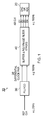
- FIG. 1 presents a schematic view of a system 10 in which clock signals are generated and supplied to DAC or ADC circuitry 20.
- a reference clock signal e.g. at 2 GHz
- a differential pair of clock signals e.g. at 16 GHz
- PLL phase lock loop
- VCO voltage controlled oscillator
- Further buffer and polyphase filter stages 40 follow to eventually (in an ideal case) output a perfect 4 ⁇ (4-phase) clock signal, e.g. with the phases at 0°, 90°, 180° and 270°, respectively.
- the output 4-phase clock signal is input to the DAC or ADC circuitry 20, for example to control output/sampler switches (as will be explained in more detail below).
- the output clock signals may be referred to as clock signals CLK ⁇ 1 to CLK ⁇ 4, being respective phases of the four-phase clock signal, as indicated in Figure 1 .
- Figures 2 to 4 present DAC and ADC circuitry corresponding to the circuitry 20 in Figure 1 .
- Figure 2 is a schematic view of a differential switching circuit 50, which may form part of DAC circuitry 20.
- the circuitry 50 comprises a common node CN (or tail node) to which a current source (or, once and for all, sink) is connected.
- a current source or, once and for all, sink
- transistors SW1 to SW4 are shown connected in parallel (in parallel branches) between the common node CN and a first output node A.
- transistors SW5 to SW8 are shown connected in parallel between the common node CN and a second output node B.
- These transistors SW1 to SW8 will be referred to as output switches hereafter, and correspond to the output switches mentioned in connection with Figure 1 .
- the gates of the output switches SW1 to SW8 are driven directly by way of clock signals CLK ⁇ 1 to CLK ⁇ 4 as indicated, although a buffer or decoupling capacitor may be provided along the clock paths to the gates (not shown).
- Data-controlled switches D1 to D8 are provided in series connection with the output switches SW1 to SW8, respectively. Data-controlled switches D1 to D8 are driven by respective data signals as shown and described below.
- each output switch SW1 to SW8 effectively is one of a pair of series-connected switches (in this case, field-effect transistors). These switches may be implemented as NMOS field-effect transistors.
- the clock signals CLK ⁇ 1 to CLK ⁇ 4 are substantially sinusoidal in the present example. Effectively, four time-interleaved sinusoidal clock signals are provided.
- the overall operation of the Figure 2 circuitry is that the output switches SW1 to SW8 and the data-controlled switches D1 to D8 are driven so as, in use, to steer current from the current source through the first output node A or the second output node B in dependence upon the value (digital 0 or 1) of the data signals DATA1 to DATA4, which are shown as being applied to the data-controlled switches D1 to D8.
- output switches SW1 and SW5 are provided with clock signal CLK ⁇ 1, SW2 and SW6 are provided with clock signal CLK ⁇ 2, SW3 and SW7 are provided with clock signal CLK ⁇ 3, and SW4 and SW8 are provided with clock signal CLK ⁇ 4.
- data-controlled switches D1 and D5 are respectively provided with data signals DATA 1 and DATA1
- D2 and D6 are respectively provided with DATA 2 and DATA2
- D3 and D7 are respectively provided with DATA 3 and DATA3
- D4 and D8 are respectively provided with DATA 4 and DATA4 .
- output switch SW1 or SW5 carries a current pulse in a first clock cycle or phase ( ⁇ 1), dependent on the value of the data signal DATA 1.
- SW2 or SW6 carries a current pulse in a second clock cycle or phase ( ⁇ 2)
- SW3 or SW7 carries a current pulse in a third clock cycle or phase ( ⁇ 3)
- SW4 or SW8 carries a current pulse in a fourth clock cycle or phase ( ⁇ 4).
- the output switches in Figure 2 are NMOS transistors, and as such turn on in the +ve peak portions of the relevant clock signals.
- Output nodes A and B are connected to the output switches via respective output cascodes as indicated in Figure 2 .
- a differential analogue output signal of the switching circuitry (corresponding to the input digital data) may thus be measured between the two output terminals, as a current signal or as a voltage signal by way of terminating resistors (not shown).
- each pair of series-connected switches in Figure 2 is off and 7 are on. Looking at the upper switches (the output switches) of each pair, in any state 2 are on and 6 are off. Looking at the lower switches (the data-controlled switches) of each pair, in any state (ignoring transitional changes of the data values, which in an ideal case would be instantaneous) 4 are on and 4 are off.
- each pair looking at each pair as a single unit, from one cycle to the next 1 turns on and 1 turns off. Looking at the upper switches (the output switches) of each pair, from one cycle to the next 2 turn on and 2 turn off. Looking at the lower switches (the data-controlled switches) of each pair, from one cycle to the next either the same number turn on as turn off (if the data changes) or the switches retain their states (if the data stays the same).
- the circuitry portion comprising output switches SW1 to SW8 may be referred to as clock-controlled circuitry 52, and the circuitry portion comprising data-controlled switches D1 to D8 may be referred to as data-controlled circuitry 54.
- the switches in the clock-controlled circuitry 52 are controlled by clock signals and not by data signals, and as such they may be considered data-independent.
- the switches in the data-controlled circuitry 54 are controlled by data signals and not by clock signals, and as such they may be considered clock-independent.
- the clock signals CLK ⁇ 1 to CLK ⁇ 4 may be supplied continuously (i.e. during active operation) to the clock-controlled circuitry 52 and specifically to the gates of the output switches SW1 to SW8 (field-effect transistors).
- Figure 4 presents waveforms for the clock signals CLK ⁇ 1 to ⁇ 4 in the upper graph, and partial waveforms for the currents received at output nodes A and B, labeled as IOUT A and IOUT B , in the lower graph, for use in better understanding the operation of differential switching circuit 50 of Figure 2 .
- clock signals CLK ⁇ 1 to ⁇ 4 are time-interleaved raised (substantially) cosine waveforms and are 90° out of phase with one another.
- the clock signals shown are sinusoidal, but need not be strictly-perfect sinusoids. As will become apparent, in the present embodiment the shape of the waveforms is more important in the uppermost part than towards the bottom.
- the number of clock signals shown in Figures 3 and 4 is related to the number of parallel paths to each of nodes A and B in Figure 2 . Since there are four parallel paths to each of nodes A and B in Figure 2 , four time-interleaved clock signals are provided, 90° out of phase with one another. It is envisaged that where X parallel paths to each of nodes A and B are provided, X time-interleaved clock signals may be provided, (360/X)° out of phase with one another. In this case, X is an integer greater than or equal to 2, and preferably greater than or equal to 3, and more preferably equal to 4.
- clock signal ⁇ 4 is highlighted in bold.
- Clock signals CLK ⁇ 1 to ⁇ 4 control the gates of output switches SW1 to SW8, as already described in connection with Figure 2 . Accordingly, the output-switch pairs (where the pairs are SW1/SW5, SW2/SW6, SW3/SW7, SW4/SW8) are turned on and then off in sequence, such that as one of them is turning off the next in sequence is turning on, and such that when one of them is turned fully on the others are substantially turned off. As mentioned before, which switch of such an output-switch pair carries a current pulse when the pair is turned on is dependent on the data signal (of DATA 1 to DATA 4) concerned.
- the differential switching circuit 50 of Figure 2 effectively operates in current-mode, steering current I TAIL between the available paths. Because substantially all current passing through the common node via switches SW1 to SW8 must equal current I TAIL , then the sum of currents flowing through nodes A and B at any time must be substantially equal to I TAIL . The effect of the data-controlled switches D1 to D8 mentioned above is therefore that current I TAIL is steered to pass through one switch from each output-switch pair in the sequence in which those output-switch pairs are turned on and off, i.e.
- waveform ⁇ 4 is rising towards its peak value but has not yet reached its peak value. Also, at point 79, waveform ⁇ 3 is falling from its peak value.
- clock signals ⁇ 3 and ⁇ 4 have equal values. Therefore switches SW3 and SW4, and also SW7 and SW8 are on to the same extent as one another, because their source terminals are connected together.
- clock signals ⁇ 1 and ⁇ 2 are also equal to one another and are sufficiently low to ensure that switches SW1 and SW2, and also SW5 and SW6, are off.
- points 70, 72 and 74 for current waveform IOUT A in Figure 4 are fixed or defined in time relative to the clock waveforms and in magnitude relative to the current I TAIL . That is, taking current IOUT A as an example, at point 70 the current is equal to I TAIL and at points 72 and 74 the current is equal to half I TAIL . The location of points 70, 72 and 74 is fixed relative to the clock signals ⁇ 1 to ⁇ 4 . The same is true for the subsequent current signal pulses or charge packets, which may be for IOUT A or IOUT B dependent on the data.
- the focus on points 60, 62 and 64 demonstrates that the upper part of the clock signals is important, and that the lower parts are less important (such that, for example, the precise shape of the lower parts is not strictly critical).
- the series of current pulses of waveforms are all of the same shape, and that shape is defined by the raised cosine shape of the clock signals.
- the data value concerned should be stable in time to create the pulse concerned.
- the relevant data signal DATA 4 should be stable at least over the period of time spanning the five vertical dashed lines.
- data signal DATA 4 could be arranged to change state at or approximately at the troughs (negative peaks) of clock signal CLK ⁇ 4 .
- each of data signals DATA 1 to DATA 3 could be arranged to change state at or approximately at the troughs of their respective clock signals CLK ⁇ 1 to ⁇ 3 .
- the data signals DATA 1 to DATA 4 may also be 16 GHz signals configured to change state at or approximately at the troughs of their respective clock signals.
- the point to note is that the accuracy of the clock signals CLK ⁇ 1 to ⁇ 4 directly affects the accuracy of the current pulses in the lower part of Figure 4 , and as a result the accuracy of the overall DAC circuitry.
- FIG. 5 presents sampling circuitry 80, which may form part of ADC circuitry 20.
- FIG. 5 corresponds to Figure 10 of EP-A1-2211468 , to which reference may now be made.
- sampling switches SW1 to SW8 correspond to output switches SW1 to SW8 of Figure 2
- clock signals CLK ⁇ 1 to ⁇ 4 also correspond to clock signals CLK ⁇ 1 to ⁇ 4 of Figures 2 to 4 .
- the relative importance of the uppermost parts of the clock signals CLK ⁇ 1 to ⁇ 4 explained in connection with Figure 3 also applies to the sampling circuitry 80 of Figure 5 , as explained in Figure 12 of EP-A1-2211468 .
- a detailed understanding of the sampling circuitry 200 can be found in EP-A1-2211468 .
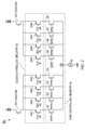
- Each buffer stage 100 comprises one or more buffers per channel CH1 to CH4, where each channel carries a different phase ( ⁇ ) of the 4 ⁇ clock signal.
- CH1 carries CLK ⁇ 1 of phase 1
- CH2 carries CLK ⁇ 2 of phase 2
- CH3 carries CLK ⁇ 3 of phase 3
- CH4 carries CLK ⁇ 4 of phase 4.
- the buffer stage 100 comprises two buffers 102 per channel, arranged into two parallel sets 104 of four buffers.
- Such buffers and buffer stages (and buffer circuitry) may be considered to be circuitry which provides electrical impedance transformation from one circuit to another.
- Each polyphase filter stage may also comprise one or more such buffer stages 100 of parallel sets 104 of buffers 102.
- the polyphase filter stage 110 (which may represent part of a polyphase filter stage) presented in the middle part of Figure 6 comprises a parallel set 104 of buffers 102, along with an RC network 112 comprising series resistances 114 per channel, and capacitances 116 coupling adjacent channels.
- Buffer circuit 120 is essentially a CMOS inverter, comprising NMOS and PMOS field-effect transistors (FETs) coupled as shown.
- FETs field-effect transistors
- Figure 7 indicates that several buffer/polyphase-filter stages may be provided in series to bring the 4 phases ( ⁇ ) on the respective channels CH1 to CH4 towards the ideal case. That is, in each successive stage the phase angles come closer towards an ideal case of 0°, 90°, 180° and 270°.
- Known buffer circuitry 120 as shown in Figure 6 on the right-hand side is not sufficiently accurate (when using multiple such buffers 102 together, particularly in parallel set 104).
- random V TH (threshold voltage) variation in the NMOS and PMOS field-effect transistors (FETs) of the buffer circuitry lead to variations in the switching delays and thus performance of the buffers 102.
- This V TH (threshold voltage) variation is a variation in the sense that one such transistor may have a different threshold voltage from the next, both across process (e.g. from chip to chip) and within the same process (e.g. within the same chip).
- the parallel set of buffers 104 across the four channels be delay-matched to better than 100fs, to enable sufficiently accurate operation when using 16 GHz clocks.
- This is a significant design factor.
- the transistors need to be very small (low-power) high-speed transistors to carry such 16 GHz clock signals, and at such sizes the variation in threshold voltage V TH (both across process and also within the same process) is significant and causes too much variation in delay between buffers.
- inductors which, although they may be used in other circuitry, are suitable for use in such buffer circuitry in which a high degree of matching is desired. It has been found, again as described later herein, that existing inductors detrimentally affect matching performance.
- buffer circuitry comprising: a switching arrangement comprising at least one signal-path switch configured to switch in dependence upon an input signal, and operable to output an output signal based on such switching, the switching of each said signal-path switch affecting the output signal; and a current-control arrangement, wherein: the switching performance of the buffer circuitry is dependent on a bias current which flows through each said signal-path switch of the switching arrangement; and the current-control arrangement is connected to the switching arrangement and configured to (control or) define the bias current which flows through (at least one or) each said signal-path switch so as to control the switching performance of the buffer circuitry.
- the input signal may be a switched-logic signal such as a digital signal, or an analogue signal such as a sinusoidal signal.
- Such signal-path switches may be in the path between the input and output signals, in the sense that their switching is controlled by the input signal (e.g. directly) and in the sense that their switching affects the magnitude of the output signal directly.
- the buffer circuitry may have an output at which the output signal is produced, and each signal-path switch may be directly or indirectly connected to that output.
- the switching performance of the circuitry may be defined by switching delays of the or each signal-path switch.
- the present invention advantageously enables the switching performance of the buffer circuitry to be matched with (e.g. made similar to or the same as, or brought within a close range of) a given performance, which may be that of another set of buffer circuitry.
- the present invention may enable improved matching between plural sets of such buffer circuitry.
- the present invention may enable such matching to be achieved despite the phenomenon of threshold voltage variation in such switches (e.g. field-effect transistors).
- the current-control arrangement may be configured to individually define the bias current which flows through (at least one or) each said signal-path switch.
- the current-control arrangement may be configured to define the bias current which flows through (at least one or) each said signal-path switch substantially independently of a difference between a threshold voltage of that switch and a reference threshold voltage.
- the switching arrangement may comprise at least two signal-path switches.
- the current-control arrangement may be configured to define the bias current which flows through (at least one or) each of those signal-path switches substantially independently of a difference between a threshold voltage of that switch and a corresponding reference threshold voltage, and/or substantially independently of a difference between threshold voltages of those switches.
- the current-control arrangement may be configured such that a range in which each said bias current is expected to lie is narrower than if said current-control arrangement were not provided. That is, the current-control arrangement may be inherently easier to match (with a given current-control arrangement) than is said signal-path switch (with a given signal-path switch).
- the current-control arrangement may be configured such that a range in which each said bias current is expected to lie is N times narrower than if said current-control arrangement were not provided, where 1 ⁇ N ⁇ 20, and optionally where 2 ⁇ N ⁇ 5.
- the current-control arrangement may comprise at least one current-control switch, such switches being configured to define the bias current which flows through (at least one or) each said signal-path switch.
- Such current-control switches may be non-switching switches, in the sense that they are not switched based on the input signal. As such, they may be considered to be out of the signal path, and instead control the operation of the signal-path switches. Such current-control switches may serve as part or all of current sources or sinks.
- the size of the or each current-control switch may be large as compared to the size of the or each signal-path switch, such that a range in which each bias current is expected to lie is narrower than if the current-control arrangement were not provided. Larger switches may be easier to match (in terms of threshold voltage) than smaller switches.
- the size of the or each current-control switch may be X times larger than the size of the or each signal-path switch, where 2 ⁇ X ⁇ 1000, and preferably where 10 ⁇ X ⁇ 500, and more preferably where 80 ⁇ X ⁇ 150.
- the or each switch may be a field-effect transistor.
- the size of such switches may be defined by their gate area, or by one or both of the length and width of their channels.
- the switching arrangement may comprise at least two signal-path switches, and those two signal-path switches may be PMOS and NMOS field-effect transistors configured as a CMOS inverter having an input at which said input signal is received and an output at which the output signal is output.
- the current-control arrangement may comprise a PMOS field-effect transistor, being a current-control switch, and that PMOS field-effect transistor may be connected in series with the PMOS field-effect transistor of the inverter so as to define the bias current which flows through the PMOS field-effect transistor of the inverter.
- the current-control arrangement may comprise an NMOS field-effect transistor, being a current-control switch, and that NMOS field-effect transistor of the current-control arrangement may be connected in series with the NMOS field-effect transistor of the inverter so as to define the bias current which flows through the NMOS field-effect transistor of the inverter.
- the input and output of the inverter may be coupled together via a resistor, the input may be connected to receive the input signal via a decoupling capacitor, and a node between the field-effect transistor of the current-control arrangement and the inverter may be coupled to a reference voltage via a capacitor. This may enable the field-effect transistor of the current-control arrangement to define the bias currents which flow through both the PMOS and NMOS field-effect transistors of the inverter.
- the current-control arrangement may comprise an NMOS field-effect transistor, being a current-control switch
- the NMOS field-effect transistor of the current-control arrangement may be connected in series with the NMOS field-effect transistor of the inverter so as to define the bias current which flows through the NMOS field-effect transistor of the inverter
- each of the NMOS and PMOS field-effect transistors of the current-control arrangement may be coupled at a node between itself and the inverter transistors to a reference voltage via a capacitor. This may enable the field-effect transistors of the current-control arrangement to define the bias currents which flow through both the PMOS and NMOS field-effect transistors of the inverter.
- Such buffer circuitry may comprise a reactance coupled to the input and/or output of the inverter and configured so as to control the frequency response of the buffer circuitry.
- the reactance may comprise an inductor and/or a capacitor, optionally wherein either or both of them are tuneable, optionally by switching in or out inductors/capacitors.
- Such an inductor may be an inductor arrangement as in the seventh or eighth aspect described below.
- the switching arrangement may comprise at least two signal-path switches being transistors, and the current-control arrangement may comprise at least one current-control switch for each signal-path switch, each connected to define the bias current which flows through its signal-path switch.
- each signal-path may be provided with its own current source or sink.
- the at least two signal-path switches may be field-effect transistors of the same channel type.
- buffer circuitry comprising: a CMOS inverter comprising PMOS and NMOS field-effect transistors, and operable to receive an input signal and output an output signal based on switching of those PMOS and NMOS field-effect transistors in response to that input signal; and a PMOS field-effect transistor configured to act as a current-control switch and connected in series with the PMOS field-effect transistor of the inverter so as to define a bias current which flows through the PMOS field-effect transistor of the inverter; and an NMOS field-effect transistor configured to act as a current-control switch and connected in series with the NMOS field-effect transistor of the inverter so as to define a bias current which flows through the NMOS field-effect transistor of the inverter.
- the size of the field-effect transistors configured to act as current-control switches may be large as compared to the size of the field-effect transistors of the inverter.
- the or each bias current may be an average current or an effective DC current.
- the input signal may be a high-speed signal, and the or each current-control switch may be controlled by a low-speed signal.
- the input signal may cause the, or each signal-path switch to switch so as to define signal transitions in said output signal, and the or each current-control switch may be controlled by a signal which tunes or biases the performance or gain of that switch rather than causes it to switch.
- the or each current-control switch may be configured as a non-switching switch, to act as part or all of a current source or sink.
- Buffer circuitry of either of the aforementioned first and second aspects may comprise an inductor arrangement as in the seventh or eighth aspect described below.
- signal distribution circuitry comprising a plurality of sets of buffer circuitry according to either of the aforementioned first and second aspects.
- signal distribution circuitry comprising: first buffer circuitry according to either of the aforementioned first and second aspects; and second buffer circuitry according to either of the aforementioned first and second aspects, wherein: the switching arrangement of the second buffer circuitry is configured in the same way as the switching arrangement of the first buffer circuitry; and the current-control arrangement of the second buffer circuitry is configured in the same way as the current-control arrangement of the first buffer circuitry, so as to tend to cause the switching performance of the second buffer circuitry to be the same as the switching performance of the first buffer circuitry.
- the second buffer circuitry may be connected so as to receive as its input signal the output signal of the first buffer circuitry.
- respective input signals of the first buffer circuitry and the second buffer circuitry may be different clock signal phases of a multi-phase time-interleaved clock signal.
- analogue-to-digital converter circuitry or digital-to-analogue converter circuitry comprising buffer circuitry according to either of the aforementioned first and second aspects, or signal distribution circuitry according to either of the aforementioned third and fourth aspects.
- an integrated circuit or an IC chip comprising circuitry according to any of the aforementioned first to fifth aspects.
- an integrated circuit comprising an inductor arrangement, the arrangement comprising: four inductors adjacently located in a group and arranged to define two rows and two columns, wherein: the integrated circuit is configured to cause two of those inductors diagonally opposite from one another in the arrangement to produce an electromagnetic field having a first phase, and to cause the other two of those inductors to produce an electromagnetic field having a second phase, the first and second phases being substantially in antiphase.
- Such inductors may be discrete inductors, i.e. distinct from one another even if they are connected together.
- the rows and columns may be regularly or irregularly arranged. For example, the rows may be perpendicular to the columns.
- the spacing between the inductors may be regular (e.g. defining a regular grid or array) or irregular.
- the inductors may have the same dimensions as one another, or different dimensions.
- the inductors may be formed on the same layer or layers of the integrated circuit as one another, or on different layers.
- the direction of turns of the inductors may be the same as one another, or different.
- the width and length of the tracking which makes up the inductors may be the same for all of the inductors, or there may be differences.
- the first and second phases may be stable or may shift, while remaining (at least mainly or for particular periods) in antiphase.
- Such integrated circuitry may be advantageous in that the inductor arrangement has little or no or negligible impact (in the sense of electromagnetic interference) on surrounding circuitry such as other inductors.
- the integrated circuitry may have one or more layers, e.g. metal layers, wherein each inductor is formed in only one such layer or across a plurality of such layers.
- the inductors may each have one or more turns, and may be spiral inductors.
- the inductors may have the same size and number of turns as one another.
- the direction of the turns of the inductors may be configured so that they produce their respective electromagnetic fields.
- the inductors may be connected to other circuitry of the integrated circuit and/or to each other so that they produce their respective electromagnetic fields.
- the inductors may be immediately adjacently located, for example such that no other circuitry components are located between those inductors.
- a spacing between effective centres of the inductors may be Z times an effective diameter of at least one of the inductors, where 1 ⁇ Z ⁇ 50, and preferably where 1 ⁇ Z ⁇ 10, and more preferably where 2 ⁇ Z ⁇ 5.
- An effective centre may be the centre of a circle which is defined by an outer periphery of an inductor, when viewed in plan view.
- the arrangement may comprise sixteen inductors including said four inductors.
- the inductors may be arranged to define four rows and four columns, and be configured so that each of them produces an electromagnetic field having the first phase or the second phase.
- diagonally opposite inductors may produce electromagnetic fields having the same phase as one another.
- the group of the arrangement may comprise any number of inductors greater than four.
- the electromagnetic fields may be fluctuating or alternating fields, for example with a predominant centre frequency (or characteristic frequency).
- the electromagnetic fields may have the same centre frequency or characteristic frequency.
- the inductors of the arrangement may be connected together to form or act as a single inductor or two separate inductors. That is, the inductors of the arrangement may be conductively connected together, or pairs of them may be conductively connected together, the pairs themselves not being conductively connected to one another. The inductors of the arrangement may be connected to different circuits, and not be conductively connected together.
- Such an integrated circuit may comprises first and second such inductor arrangements, wherein: the first and second phases of the first inductor arrangement are substantially in quadrature with the first and second phases, respectively, of the second inductor arrangement.
- Such an integrated circuit may be adapted to handle four clock signals being the four phases of a four-phase clock signal.
- such an integrated circuit may comprise buffer circuitry adapted to receive and buffer four clock signals being the four phases of a four-phase clock signal, wherein: the first and second inductor arrangements are connected to the buffer circuitry such that their electromagnetic fields are generated from respective ones of those clock signals.
- the or each inductor arrangement may define associated null lines along which its effective electromagnetic field has zero or negligible field strength. That is, along such lines the combination of the electromagnetic fields produced by the inductors may have zero or negligible field strength.
- each may be located substantially along one of the other's null lines.
- Such first and second inductor arrangements and the buffer circuitry may form a first clock distribution unit.
- the integrated circuit may comprise a second such clock distribution unit, and the first and second clock distribution units may be connected such that the clock signals having been buffered by the buffer circuitry of the first clock distribution unit are the clock signals received by the buffer circuitry of the second clock distribution unit.
- Each inductor arrangement may define associated null lines along which its effective electromagnetic field has zero or negligible field strength
- the first and second inductor arrangements of the first clock distribution unit may each be located substantially along one of each other's null lines
- the first inductor arrangements of the first and second clock distribution units may each be located substantially along one of each other's null lines
- the second inductor arrangements of the first and second clock distribution units may each be located substantially along one of each other's null lines.
- an integrated circuit comprising an inductor arrangement, the arrangement comprising: a plurality of (optionally spiral) inductors adjacently located in rows and columns, wherein: the inductors are connected so as to produce an electromagnetic field having a first or second phase, the first and second phases being substantially in antiphase; and adjacent inductors in said one or more rows or columns produce electromagnetic fields having different said phases.
- the plurality may be a group of four. The number of rows and columns may be equal.
- An integrated circuit according to the aforementioned seventh or eighth aspect of the present invention may comprise analogue-to-digital converter circuitry and/or digital-to-analogue converter circuitry.
- An integrated circuit according to the aforementioned seventh or eighth aspect of the present invention may comprise buffer circuitry according to either of the aforementioned first and second aspects, or signal distribution circuitry according to either of the aforementioned third and fourth aspects.
- an IC chip comprising an integrated circuit according to the aforementioned seventh or eighth aspect of the present invention.
- the present invention extends to method aspects corresponding in scope with the aforementioned aspects of the present invention.
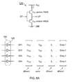
- the present inventors have considered how to improve control of buffer circuitry and mitigate mismatch-related issues.
- the threshold voltages V TH of the two transistors govern the bias/average current I that flows through them, which governs the switching delay.
- Figure 8A presents buffer circuitry 120 again, in its upper portion.
- the same NMOS and PMOS field-effect transistors (FETs) are shown, and indicated as being susceptible to V TH variation. That is, the threshold voltages in one such buffer may be different from those in another such buffer.
- a current I here, schematically representing an average or bias current
- a parallel set 104 of buffers is indicated, where each buffer is implemented as buffer circuitry 120.
- V TH variation across the 4 channels CH1 to CH4 the threshold voltages V TH may be different, and as such given constant V DD , the currents I would be different giving different delays. This is indicated also in the lower part of Figure 8A , alongside the parallel set 104 of buffers.
- the respective threshold voltages V TH1 to V TH4 for the channels CH1 to CH4 are indicated as being different from one another, by way of suffixes 1 to 4 corresponding to the channel numbers.
- suffixes 1 to 4 there are two transistors per buffer, each transistor having its own threshold voltage, however for simplicity it is simply indicated that there is some difference in threshold voltage between the buffers.
- the entries for V DD , I and Delay will be understood similarly (in terms of whether or not suffixes are shown) with reference to the circuitry 120 in the upper portion of Figure 8A .
- the delays associated with the four buffers are substantially different (indicated by Delay1 to Delay 4).
- V TH may be difficult/impossible to sufficiently match across the channels (both within a process and across process, given practical manufacturing constraints), it is possible to match the currents I to a high degree (as compared to V TH matching) and thereby attempt to closely match the delays.
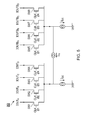
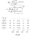
- Figure 8B presents buffer circuitry 130 devised with this in mind.
- the basic CMOS inverter structure is the same as in circuitry 120 of Figure 8A , except that the input and output are resistor-coupled with a resistance or resistor 132, and that the input is DC-decoupled from (or AC-coupled to) the preceding stage by way of a capacitor or capacitance 134, which may be referred to as an AC coupling capacitor C AC .
- a PMOS transistor 136 is provided between V DD and the PMOS transistor of the inverter, and controlled by a bias voltage Vbias to act as a current source.
- Vbias bias voltage
- a local V DD is created for the CMOS inverter transistors, also as indicated.
- the PMOS transistor 136 acting as a current source controls or defines the average or bias current flowing through both transistors of the CMOS inverter.
- the current-source PMOS transistor 136 may be relatively large (as compared to the inverter transistors) and thus it is easier to match across the channels (in terms of V TH ). That is, the threshold voltages V TH of the current-source PMOS transistor 136 may be matched to a much higher degree across different buffers 130 than the PMOS and NMOS transistors of the inverter portion itself. Therefore, even with a common Vbias across the channels (as opposed to an individual Vbias per channel), it is possible to match the bias current Ibias from the current source across the channels to a high or sufficient degree. Of course, an individual Vbias per channel could be provided.
- a parallel set 104 of buffers is indicated, where each buffer is implemented as buffer circuitry 130.
- each buffer is implemented as buffer circuitry 130.
- Ibias may be the same across the channels (with the effect of differences in local V DD across the channels) and as such also the delay. This is indicated also in the lower part of Figure 8A , alongside the parallel set 104 of buffers.
- the respective threshold voltages V TH1 to V TH4 for the channels CH1 to CH4 are indicated as being different from one another, by way of suffixes 1 to 4 corresponding to the channel numbers, as in Figure 8A .
- the entries for local V DD , Ibias and Delay will be understood similarly with reference to the circuitry 130 in the upper portion of Figure 8B .
- the currents (Ibias) and the delays (Delay) associated with the four buffers are substantially matched, or approximately the same (indicated by the entries Ibias and Delay being the same for all channels).
- the PMOS current source (current-control device, current-control switch) provided in Figure 8B individually defines the average or bias currents of both transistors (signal-path switches) of the CMOS inverter.
- the average or bias currents of both transistors of the CMOS inverter are defined substantially independently of: (a) the threshold voltages of those transistors; (b) differences between those threshold voltages, and/or (c) differences between those threshold voltages and corresponding reference threshold voltages (for example, expected ideal/target threshold voltages).
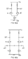
- Figures 9(a) and 9(b) present respective sets of buffer circuitry, to indicate that the inverter arrangement in circuitry 130 is not essential. That is, the inverter arrangement may be considered one example of a switching arrangement comprising at least one signal-path switch configured to switch in dependence upon an input signal, where the switching performance of the buffer circuitry is dependent on a bias current flowing through the or each signal-path switch of the switching arrangement. Similarly, the current source 136 may be considered one example of a current-control arrangement connected to the switching arrangement and configured to control the bias current flowing through the or each signal-path switch so as to control the switching performance of the buffer circuitry.
- the buffer circuitry of Figure 9(a) which is provided as a comparative example, comprise transistors M1 and M2 (implemented here as NMOS transistors), each of which is connected via a resistance to the supply voltage V DD and which are together connected via a common current source to ground GND. M1 and M2 are connected to receive complementary input signals IN and IN and to output complementary output signals OUT and OUT as shown.
- Such circuitry may be referred to as a CML (Common-Mode Logic) buffer.
- the switching delay is affected by the threshold voltage V TH of the transistors M1 and M2. Any threshold voltage difference between M1 and M2 means that the delay is different for rising and falling edges of the input signal IN. For example, if there is such threshold voltage mismatch, the current I from the current source does not split equally on average between the two transistors M1 and M2.
- each transistor is provided with its own current source, such that transistor M1 has current source I 1 and transistor M2 has current source I 2 . Further, the transistors are now decoupled from one another via a capacitance, with further capacitances coupling the nodes between the transistors and the current sources to ground GND, as shown.
- the two transistors M1 and M2 are provided with their own current sources, so that the (bias) current flowing through them may be set by matching the current sources I 1 and I 2 .
- the current sources may be implemented as transistors having a large gate are relative to the sizes of M1 and M2 (which may be small for high-speed operation and thus have large threshold-voltage mismatch). As such, the current sources may be relatively well matched, rendering the Figure 9(b) delay-matched buffer circuitry in line with the general principle of the present invention. Essentially, even with the threshold voltage variation between M1 and M2, the bias currents and the delays are substantially matched, or approximately the same. With this principle, good matching could be achieved between several sets of the Figure 9(b) circuitry, whereas this may not be achieved in respect of the Figure 9(a) circuitry.
- Figure 10 presents buffer circuitry 140 equivalent to circuitry 130 depicted in Figure 8B , albeit in an "upside-down" form with the current source 142 corresponding to current source 136 provided below the CMOS inverter transistors. Also, the decoupling capacitor 138 is shown linking between the upper reference voltage (provided from a driver or amplifier 144) and a node between the CMOS inverter transistors and the current source 142.
- the two graphs in Figure 10 indicate how the performance (AC gain) of the buffer circuitry 140 is related to the AC coupling capacitor C AC 134 (bearing in mind that it has associated parasitic capacitances, e.g. including those associated with the tracking and the CMOS transistor gates).
- buffer AC gain over frequency is indicated for different sizes of C AC , named relative to one another as “big”, “optimal” and “small” for simplicity.
- the frequency response has been found to peak around 5 GHz as opposed to around the example clock frequency 16 GHz, giving suboptimal noise performance (or “noise peaking").
- the lower graph gives a fuller picture of the effect of varying C AC at the example clock frequency 16 GHz, and as such represents a snapshot of the upper graph at the 16 GHz point.
- the circuitry suffers from AC coupling gain loss, which varies with C AC . That is, the ideal case ("desired") where gain is independent of the value of C AC is different from the "actual” case, where gain peaks at "optimal” C AC .
- the loss is indicated as being represented by the shaded area between the "desired” (ideal) and "actual” cases.
- the knock-on effect may be high power density and potentially "hot spots" in a circuitry implementation.
- Figure 11 presents modified buffer circuitry 150, intended to address the issues identified above in connection with Figure 10 .
- the AC coupling capacitor 134 and input-to-output coupling resistor 132 are removed, and current sources 152 and 154 are provided for both the NMOS and PMOS transistors, respectively, with decoupling capacitors 156 and 158 as shown.
- nbias and pbias controls of the current sources 152 and 154 may be applied to account for variation in V THN (threshold voltage for the inverter NMOS transistor) and V THP (threshold voltage for the inverter PMOS transistor), respectively, creating a local V DD and a local V SS as shown.
- the current sources 152 and 154 may be implemented by way of field-effect transistors (which are large relative to the inverter transistors, for reasons of matching) in line with current source 136 of Figure 8B , and the nbias and pbias controls may thus be understood as gate voltages for those field-effect transistors, one (nbias) associated with the current source for the inverter NMOS transistor and the other (pbias) associated with the current source for the inverter PMOS transistor.
- An inductor L 162 and variable capacitor C TUNE 164 are provided between the buffers 150, and LC TUNE may be tuned by way of C TUNE so that the buffer gain peaks at the example clock frequency 16 GHz, taking into account the parasitic capacitances C IN and C OUT as indicated in Figure 11 .
- These capacitances C IN and C OUT are parasitic, i.e. associated with the discrete circuit elements of buffers 150, and are not discrete components themselves.
- buffer AC gain over frequency is indicated for the buffer circuitry 140 of Figure 10 and for the buffer circuitry 150 of Figure 11 , to demonstrate that LC TUNE may be tuned in circuitry 150 by way of C TUNE so that the buffer gain peaks at the example clock frequency 16 GHz.
- inductor 162 and capacitor 164 only one of them is shown as being tuneable. Of course, either or both of them could be tuneable.
- inductors and/or capacitors could be switched in or out to adjust the value of LC TUNE .
- Capacitor C TUNE 164 may be implemented for example as a varicap or a switched capacitor, or a combination of both.
- Inductor L 162 may be implemented as a switched inductor.
- the transistors forming the current sources 152 and 154 may be large (relative to the CMOS inverter transistors) and thus well matched.
- the nbias and pbias controls may accordingly be common across the 4 channels CH1 to CH4, matching the currents and thus the delays across the channels.
- the nbias and pbias controls may, in another embodiment, be separately provided.
- amplitude level control may be implemented by sensing the amplitude of the clock signals and controlling nbias and pbias accordingly. This could be done per channel or for all 4 channels in parallel.
- the choice as to whether to carry out such ALC per channel or in common for all channels depends on the accuracy/matching of the circuit that measures amplitude of the clock signals (Vpp) compared to the accuracy/matching of the circuit that sets the bias currents. If the measuring circuit is the more accurate of the two it may be better to have individual gain/bias adjustments (i.e. per channel). If, however, the measuring circuit mismatch is bigger than that of the circuit that sets the bias currents it may be better to control all bias currents together (i.e. in common across the channels).
- MOS transistor current matching does not depend on just gate area but also on the drain saturation voltage V DSAT (which roughly equals or is related to V GS -V TH , where V GS is the gate-source voltage and V TH is the threshold voltage).
- the drain saturation voltage V DSAT is the voltage beyond which the drain current is saturated, and for each gate voltage there is a different drain saturation voltage V DSAT .
- the part of the IV curve with V DS (the drain-source voltage) ⁇ V DSAT is the linear region, and the part with V DS > V DSAT is the saturation region.
- V DS and V DSAT may be thought of as equivalent to the voltage drop across the transistor device. The current mismatch between two such transistors is proportional to the difference in V TH divided by V DSAT .
- V TH mismatch is inversely proportional to gate area, so large gate area allows good V TH matching and high V DSAT allows good current matching.
- high V DSAT (which gives good current matching) also means that the transistor gain is low and switching speed is slow, and high gate area means high capacitance which also means slow switching.
- the switching transistors e.g. those of the CMOS inverter considered above
- K 5mV and 0.1 ⁇ m 2 area the V TH error would be 16mV; with V DSAT of 100mV this would give 16% current error.
- the current-source transistors in contrast, can be much bigger than the switching transistors, and have higher V DSAT , because they are not in the high-speed signal path (i.e. they are not switched by the high-speed input signal, such as a clock or data signal). See, for example, the circuitry of Figures 8B and 10 .
- the matching between the larger current-source transistors is far better than the matching between the smaller switching transistors.
- the gate area A CS of the current-source transistors is 100 times larger than the gate area A SW of the switching transistors.
- a CS may be 10 to 1000 times larger than A SW .
- the channel length L CS of the current-source transistors is around 33 times larger than the channel length L SW of the switching transistors.
- L CS may be 10 to 100 times larger than L SW .
- the channel width W CS of the current-source transistors is around 3.3 times larger than the channel width W SW of the switching transistors.
- W CS may be 1 to 10 times larger than W SW .
- Transistor area i.e. W*L
- V TH matching more area is better
- L/W affects V DSAT (higher is better)
- it is generally much more effective to increase L as much as possible while keeping V DSAT within reasonable limits
- increasing just W generally has little or no effect on current matching because V TH mismatch and V DSAT both decrease together.
- a feature of the DAC and ADC circuitry described herein, in particular of the clock generation paths and buffers (buffer circuitry) for use with the DAC and ADC circuitry, is the requirement for a large number of inductors to be implemented in a small space (i.e. on chip). To understand this better, reference may be made back to, for example, Figure 11 which shows an example buffer 150, and Figures 1 , 6 and 7 .
- each buffer stage 100 comprises one or more buffers per channel.
- Each polyphase filter stage 110 may also comprise one or more sets 104 of buffers or such buffer stages 100.
- Figure 7 indicates that several buffer/polyphase-filter stages may be provided in series to bring the four phases on the respective channels towards the ideal case.
- inductor 162 at the output of one buffer 150 and/or at the input of the next buffer 150.
- Such inductors may be connected to ground (GND) or a reference voltage such as VDD. They also may be connected between opposing channels (CH1 and CH3, or CH2 and CH4) if the buffers 150 are implemented as differential buffers.
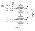
- Figure 12 is a schematic diagram demonstrating that the buffers of the buffer stages may be implemented by way of differential buffers, and is provided to further consider the importance of the inductors. If the buffer stages were implemented with differential buffers, with clock phases ⁇ 1 (0°) and ⁇ 3 (180°) dealt with by one such buffer and ⁇ 2 (90°) and ⁇ 4 (270°) by another, it could be understood that the interaction between the inductors in each differential buffer might be acceptable (since they are out of phase with one another). However, interaction between the two differential buffers would likely be problematic and may give rise to phase errors (i.e. matching errors) between the channels.
- phase errors i.e. matching errors
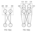
- an inductor implementation 202 is provided, in which an inductor is implemented as a pair of inductors 204 and 206 having opposite phases.
- phase error phase error reduction
- the inductors 204 and 206 are indicated as circles, with two opposing phases being indicated by “+” (PLUS) and “-” (MINUS), respectively, where PLUS and MINUS refer to the sign (DC current) or phase (AC current) of the magnetic field generated by currents through the inductors. It will be appreciated that the phases may be achieved by a combination of the direction of the turns of the inductor and the direction in which current flows through the inductor. It will also be understood that “PLUS” and “MINUS” are relative to one another, i.e. in antiphase or substantially 180° out of phase with one another.
- FIG. 13(a) Also shown in Figure 13(a) is a second pair of inductors similar to 204 and 206, in the lower portion of the Figure. Arrows are then provided between the pairs to aid an explanation of interaction between the two pairs.
- any interaction between the lower PLUS inductor and the upper PLUS inductor (of the pair) is compensated for largely by interaction between the lower PLUS inductor and the upper MINUS inductor (of the pair).
- a similar point could be made looking at interaction between the lower MINUS inductor and the pair of inductors, as indicated by the relevant arrows.
- an inductor implementation 212 is provided in accordance with the present invention, in which an inductor is implemented as a group of four inductors 214, 216, 218 and 220, where two have the opposite phase from the other two, and where like phases are diagonally opposite from one another.
- phase error reduction (than with implementation 202) can be obtained by locating inductors having opposite phases in adjacent groups of four, where like phases are diagonally opposite from one another. This may be referred to as a "cross-quad" group, and such a group is indicated by implementation 212.
- the lower PLUS inductor interacts with each of the four inductors of the cross-quad group.
- the effect of the cross-quad group 212 on the lower PLUS inductor is virtually non-existent, or at least very small, with the combination of the individual interactions (arrows) leading to substantial cancelation.
- a similar point could be made looking at the effect of the cross-quad group 212 on the lower MINUS inductor.
- the four inductors of the cross-quad group may be considered to be arranged in a two-by-two arrangement on a 2D surface (a semiconductor chip), e.g. with two rows and two columns.
- the arrangement may be considered to be a 2D arrangement, i.e. on a surface or in practice on a semiconductor chip (although, as below, this may include implementations which take up more than one layer of the chip).
- the arrangement of the inductors has the appearance of a grid of dots (each dot being an inductor), the dots being regularly arranged. Such a grid may be considered to be based on "square" or "rectangular" cells.
- the arrangement may be considered to be a matrix or rectangular/square array of inductors, defining one or more rows and columns.
- the inductors may be implemented in practice as coils which may be planar and may have a spiral form, implemented in the metal layers (i.e. with metal tracking) of a semiconductor chip.
- Such spirals may be considered to be "generally" planar, in the sense that they may be implemented over more than one layer of the chip.
- the spirals may have the appearance of planar spirals when the semiconductor chips is viewed in plan view (i.e. down through the layers from its upper surface), with the different layers superimposed on one another.
- parts of the coils occupying different such layers may overlap when the chip is viewed in plan view (e.g. as in a helical coil).
- Such coils may have one or more turns.
- Figures 14(a) and 14(b) present the pair 202 and cross-quad group 212 again, to further indicate a benefit of the cross-quad group 212 as compared to the pair 202.
- the pair 202 (when considered as an electromagnetic transmitter or receiver) has a null running vertically between the two inductors.
- the cross-quad group 212 however has two nulls, one running vertically through the middle of the group and the other horizontally through the middle of the group.
- the cross-quad group 212 offers more potential locations (i.e. along the nulls) where other inductors could be located for reduced interaction therebetween.
- the arrangement of the cross-quad group is such that it has only a small (i.e. negligible) interaction on any adjacent inductor, regardless of the phase carried by that adjacent inductor. This would be true even with reasonable - i.e. close - spacing between inductor quad groups. In effect the group has little or no effect on its surroundings.
- phase of the lower inductors in Figure 13(b) are the same as phases of the cross-quad group, the group would also have only a small interaction with inductors having other phases.
- the cross-quad group were to carry phases ⁇ 1 (0°) and ⁇ 3 (180°), it would have only a small interaction with an adjacent inductor carrying phase ⁇ 2 (90°) or ⁇ 4 (270°), or only a small interaction with an adjacent cross-quad group carrying phases ⁇ 2 (90°) and ⁇ 4 (270°).
- inductors or inductor groups By locating inductors or inductor groups relative to one another along nulls as in Figure 14 , for example so that their nulls align, better isolation is achieved than if they were to be located without aligning the nulls.
- Capacitive coupling reduces with distance D having a 1/D relationship and can be greatly reduced further or almost eliminated by adding conductive metal shields in between circuits.
- magnetic coupling reduces more slowly with distance D having a 1/[log D] relationship (see below), and shields are less effective because on-chip metals (e.g. aluminium, copper) have low permeability.
- on-chip metals e.g. aluminium, copper
- Figure 15 presents four possible configurations of the cross-quad group of Figure 13(b) , and is provided to indicate that what is important in the cross-quad group is that the inductors of the group carry two opposite phases (i.e. in antiphase) and that like phases are diagonally opposite from one another. It is this, rather than any particular connections between the inductors of the group, which provides the desired effect.
- Figure 16 presents four possible configurations of an inductor of a cross-quad group, implemented as flat spiral.
- the direction of coil winding in each inductor can be either clockwise or anticlockwise, and it is possible to connect an inductor in different ways and to different phases of the clock generation circuitry.
- Figures 16(a) to 16(d) simply show how PLUS and MINUS phases for the inductors may be generated using a single input clock phase (e.g. ⁇ 1). If the opposite clock phase (e.g. ⁇ 3) were to be input instead, of course the PLUS and MINUS phases would be reversed in Figure 16 .
- PLUS and MINUS are phases relative to one another as mentioned above, as the field in each inductor alternates over time with the input sinusoidal clock signals.
- the magnetic coupling may be considered as: Single: 1/log(D) Pair: 1/log(D).D Cross-quad: 1/log(D).D 2 Next-larger group: 1/log(D).D 3 where D is distance.
- the next number of inductors which could form a group with a similar effect beyond 4 is realistically 16.
- the number should be even for PLUS and MINUS to give acceptable cancellation; if each individual inductor (or the overall array) is rectangular, the next sizes up could be 6 or 8, but to get a real increase in isolation (1/log(D).D 3 as above) a group of 16 would be the next step up.
- a group of 4 cross-quad group
- a cross-quad group embodying the present invention may form part of a larger group of inductors (e.g. a group of 16), so that such a larger group embodies the present invention.
- Figure 17 indicates schematically how differential buffer stages DB could be provided one after the other along the clock generation path, with each differential buffer having for example two cross-quad groups of inductors. Only two successive buffer stages are shown, however many may be provided.
- each cross-quad group is represented by a group of four circles in a similar manner as in Figure 13(b) , and as such each differential buffer stage DB is shown having one cross-quad group below it and one above it.
- the buffers here are differential buffers, the upper buffer stages are shown handling (opposing) phases ⁇ 1 and ⁇ 3, and the lower stages are shown handling (opposing) phases ⁇ 2 and ⁇ 4.
- Figure 18 also indicates schematically how differential buffer stages DB could be provided one after the other along the clock generation path, but with each differential buffer having for example one cross-quad group of inductors.
- the circuitry laid out as in Figure 17 may be difficult to implement, given the need for connections between the phases in PPFs as mentioned earlier (see for example network 112 in Figure 6 ).
- the two differential buffers in each stage are adjacently located, with the cross-quad groups arranged towards the outside of the pair of differential buffers.
- a cross-quad group carrying phases ⁇ 1 and ⁇ 3 is shown at the top, then the ⁇ 1/ ⁇ 3 differential buffer, then the ⁇ 2/ ⁇ 4 differential buffer, and then a cross-quad group carrying phases ⁇ 2 and ⁇ 4 at the bottom. PPF connections may then be made between the central differential buffers.
- null lines are presented in dashed form in line with Figure 14(b) , to demonstrate that the cross-quad groups are arranged with their nulls aligned.
- the saving provided by the present invention as compared to conventional inductors may be very significant; for example, if conventional inductors need 2x/3x/4x spacing to reduce coupling between those inductors, circuit area with conventional inductors could be up to 4x/9x/16x larger.
- the present disclosure extends to buffer circuitry in accordance with the present invention and an inductor arrangement in accordance with the present invention in combination.
- the inductor 162 in the circuitry 150 may be implemented as (or part of) a cross-quad group of inductors as described above.
- Circuitry of the present invention may from part of an analogue-to-digital converter. Circuitry of the present invention may be implemented as integrated circuitry, for example on an IC chip.
- the present invention extends to integrated circuitry and IC chips as mentioned above, circuit boards comprising such IC chips, and communication networks (for example, internet fiber-optic networks and wireless networks) and network equipment of such networks, comprising such circuit boards.
Priority Applications (1)
| Application Number | Priority Date | Filing Date | Title |
|---|---|---|---|
| EP20130184036 EP2849338A1 (de) | 2013-09-12 | 2013-09-12 | Schaltungen, die zur Takterzeugung und Verteilung verwendbar sind |
Applications Claiming Priority (1)
| Application Number | Priority Date | Filing Date | Title |
|---|---|---|---|
| EP20130184036 EP2849338A1 (de) | 2013-09-12 | 2013-09-12 | Schaltungen, die zur Takterzeugung und Verteilung verwendbar sind |
Publications (1)
| Publication Number | Publication Date |
|---|---|
| EP2849338A1 true EP2849338A1 (de) | 2015-03-18 |
Family
ID=49150838
Family Applications (1)
| Application Number | Title | Priority Date | Filing Date |
|---|---|---|---|
| EP20130184036 Ceased EP2849338A1 (de) | 2013-09-12 | 2013-09-12 | Schaltungen, die zur Takterzeugung und Verteilung verwendbar sind |
Country Status (1)
| Country | Link |
|---|---|
| EP (1) | EP2849338A1 (de) |
Cited By (2)
| Publication number | Priority date | Publication date | Assignee | Title |
|---|---|---|---|---|
| CN106357269A (zh) * | 2016-09-07 | 2017-01-25 | 复旦大学 | 一种用于高速时间交织模数转换器中的输入缓冲器 |
| EP3217543A1 (de) | 2016-03-11 | 2017-09-13 | Socionext Inc. | Takterzeugungsschaltung |
Citations (7)
| Publication number | Priority date | Publication date | Assignee | Title |
|---|---|---|---|---|
| US5416446A (en) * | 1992-12-08 | 1995-05-16 | At&T Corp. | Digital programmable frequency generator |
| US5952892A (en) * | 1997-09-29 | 1999-09-14 | Lsi Logic Corporation | Low-gain, low-jitter voltage controlled oscillator circuit |
| US6097253A (en) * | 1999-02-12 | 2000-08-01 | Pmc-Sierra Ltd. | High speed process-controlled transresistance amplifier |
| US7305039B2 (en) * | 1998-10-30 | 2007-12-04 | Broadcom Corporation | Adaptively configurable class-A/class-B transmit DAC for transceiver emission and power consumption control |
| US7545194B2 (en) * | 2006-06-30 | 2009-06-09 | Intel Corporation | Programmable delay for clock phase error correction |
| EP2211468A1 (de) | 2009-01-26 | 2010-07-28 | Fujitsu Semiconductor Limited | Abtastung |
| US20120081163A1 (en) * | 2010-09-30 | 2012-04-05 | Leonardus Hesen | Rf duty cycle correction circuit |
-
2013
- 2013-09-12 EP EP20130184036 patent/EP2849338A1/de not_active Ceased
Patent Citations (7)
| Publication number | Priority date | Publication date | Assignee | Title |
|---|---|---|---|---|
| US5416446A (en) * | 1992-12-08 | 1995-05-16 | At&T Corp. | Digital programmable frequency generator |
| US5952892A (en) * | 1997-09-29 | 1999-09-14 | Lsi Logic Corporation | Low-gain, low-jitter voltage controlled oscillator circuit |
| US7305039B2 (en) * | 1998-10-30 | 2007-12-04 | Broadcom Corporation | Adaptively configurable class-A/class-B transmit DAC for transceiver emission and power consumption control |
| US6097253A (en) * | 1999-02-12 | 2000-08-01 | Pmc-Sierra Ltd. | High speed process-controlled transresistance amplifier |
| US7545194B2 (en) * | 2006-06-30 | 2009-06-09 | Intel Corporation | Programmable delay for clock phase error correction |
| EP2211468A1 (de) | 2009-01-26 | 2010-07-28 | Fujitsu Semiconductor Limited | Abtastung |
| US20120081163A1 (en) * | 2010-09-30 | 2012-04-05 | Leonardus Hesen | Rf duty cycle correction circuit |
Cited By (4)
| Publication number | Priority date | Publication date | Assignee | Title |
|---|---|---|---|---|
| EP3217543A1 (de) | 2016-03-11 | 2017-09-13 | Socionext Inc. | Takterzeugungsschaltung |
| US9887667B2 (en) | 2016-03-11 | 2018-02-06 | Socionext Inc. | Clock generation circuitry |
| CN106357269A (zh) * | 2016-09-07 | 2017-01-25 | 复旦大学 | 一种用于高速时间交织模数转换器中的输入缓冲器 |
| CN106357269B (zh) * | 2016-09-07 | 2020-05-26 | 复旦大学 | 一种用于高速时间交织模数转换器中的输入缓冲器 |
Similar Documents
| Publication | Publication Date | Title |
|---|---|---|
| US9705475B2 (en) | Circuitry useful for clock generation and distribution | |
| Kaçar et al. | Positive/negative lossy/lossless grounded inductance simulators employing single VDCC and only two passive elements | |
| US7453136B2 (en) | Methods, systems, and apparatus for integrated circuit capacitors in capacitor arrays | |
| US7183870B2 (en) | Resonant circuit and a voltage-controlled oscillator | |
| CN109192726B (zh) | 用于多模滤波器的电路和方法 | |
| EP2237425B1 (de) | Stromschaltungsanordnung | |
| JP2011049975A (ja) | 電圧制御発振器 | |
| US11749710B2 (en) | Adjustable multi-turn magnetic coupling device | |
| JP2010272815A (ja) | 可変インダクタ | |
| US10833685B1 (en) | Linearized wide tuning range oscillator using magnetic balun/transformer | |
| US8072280B2 (en) | Voltage-controlled oscillator | |
| US9583554B1 (en) | Adjustable ground shielding circuitry | |
| US20170126177A1 (en) | Trifilar Voltage Controlled Oscillator | |
| EP2849338A1 (de) | Schaltungen, die zur Takterzeugung und Verteilung verwendbar sind | |
| CN108352835B (zh) | 用于增加有源电感器工作范围和峰值增益的方法 | |
| Roy et al. | Realization of third-order voltage-mode/current-mode quadrature oscillator circuit employing VDCCs and all grounded capacitors | |
| CN110350870B (zh) | 一种Class-F2压控振荡器 | |
| US7061072B2 (en) | Integrated circuit inductors using driven shields | |
| US11196382B1 (en) | Oscillator with inductor and programmable capacitor bank | |
| JP4676894B2 (ja) | 共振器型発振器、及び同調コンデンサ回路 | |
| Kwok et al. | A 0.35-V 1.46-mW low-phase-noise oscillator with transformer feedback in standard 0.18-/spl mu/m CMOS process | |
| US11336246B1 (en) | Amplifier circuit | |
| Otı́n et al. | Digitally programmable CMOS transconductor for very high frequency | |
| JP5126333B2 (ja) | 共振器型発振器、及び同調コンデンサ回路 | |
| US20070146022A1 (en) | Analog frequency divider |
Legal Events
| Date | Code | Title | Description |
|---|---|---|---|
| PUAI | Public reference made under article 153(3) epc to a published international application that has entered the european phase |
Free format text: ORIGINAL CODE: 0009012 |
|
| 17P | Request for examination filed |
Effective date: 20130912 |
|
| AK | Designated contracting states |
Kind code of ref document: A1 Designated state(s): AL AT BE BG CH CY CZ DE DK EE ES FI FR GB GR HR HU IE IS IT LI LT LU LV MC MK MT NL NO PL PT RO RS SE SI SK SM TR |
|
| AX | Request for extension of the european patent |
Extension state: BA ME |
|
| RAP1 | Party data changed (applicant data changed or rights of an application transferred) |
Owner name: SOCIONEXT INC. |
|
| R17P | Request for examination filed (corrected) |
Effective date: 20150824 |
|
| RBV | Designated contracting states (corrected) |
Designated state(s): AL AT BE BG CH CY CZ DE DK EE ES FI FR GB GR HR HU IE IS IT LI LT LU LV MC MK MT NL NO PL PT RO RS SE SI SK SM TR |
|
| STAA | Information on the status of an ep patent application or granted ep patent |
Free format text: STATUS: EXAMINATION IS IN PROGRESS |
|
| 17Q | First examination report despatched |
Effective date: 20180413 |
|
| STAA | Information on the status of an ep patent application or granted ep patent |
Free format text: STATUS: THE APPLICATION HAS BEEN REFUSED |
|
| 18R | Application refused |
Effective date: 20191015 |