EP2849239A1 - Flexible display having damage impeding layer and method for manufacturing the same - Google Patents
Flexible display having damage impeding layer and method for manufacturing the same Download PDFInfo
- Publication number
- EP2849239A1 EP2849239A1 EP20140180267 EP14180267A EP2849239A1 EP 2849239 A1 EP2849239 A1 EP 2849239A1 EP 20140180267 EP20140180267 EP 20140180267 EP 14180267 A EP14180267 A EP 14180267A EP 2849239 A1 EP2849239 A1 EP 2849239A1
- Authority
- EP
- European Patent Office
- Prior art keywords
- layer
- heat
- energy
- flexible display
- light emitting
- Prior art date
- Legal status (The legal status is an assumption and is not a legal conclusion. Google has not performed a legal analysis and makes no representation as to the accuracy of the status listed.)
- Ceased
Links
Images




Classifications
-
- G—PHYSICS
- G09—EDUCATION; CRYPTOGRAPHY; DISPLAY; ADVERTISING; SEALS
- G09F—DISPLAYING; ADVERTISING; SIGNS; LABELS OR NAME-PLATES; SEALS
- G09F9/00—Indicating arrangements for variable information in which the information is built-up on a support by selection or combination of individual elements
- G09F9/30—Indicating arrangements for variable information in which the information is built-up on a support by selection or combination of individual elements in which the desired character or characters are formed by combining individual elements
-
- H—ELECTRICITY
- H10—SEMICONDUCTOR DEVICES; ELECTRIC SOLID-STATE DEVICES NOT OTHERWISE PROVIDED FOR
- H10K—ORGANIC ELECTRIC SOLID-STATE DEVICES
- H10K77/00—Constructional details of devices covered by this subclass and not covered by groups H10K10/80, H10K30/80, H10K50/80 or H10K59/80
- H10K77/10—Substrates, e.g. flexible substrates
- H10K77/111—Flexible substrates
-
- G—PHYSICS
- G09—EDUCATION; CRYPTOGRAPHY; DISPLAY; ADVERTISING; SEALS
- G09F—DISPLAYING; ADVERTISING; SIGNS; LABELS OR NAME-PLATES; SEALS
- G09F9/00—Indicating arrangements for variable information in which the information is built-up on a support by selection or combination of individual elements
-
- H—ELECTRICITY
- H10—SEMICONDUCTOR DEVICES; ELECTRIC SOLID-STATE DEVICES NOT OTHERWISE PROVIDED FOR
- H10D—INORGANIC ELECTRIC SEMICONDUCTOR DEVICES
- H10D86/00—Integrated devices formed in or on insulating or conducting substrates, e.g. formed in silicon-on-insulator [SOI] substrates or on stainless steel or glass substrates
- H10D86/01—Manufacture or treatment
- H10D86/021—Manufacture or treatment of multiple TFTs
-
- H—ELECTRICITY
- H10—SEMICONDUCTOR DEVICES; ELECTRIC SOLID-STATE DEVICES NOT OTHERWISE PROVIDED FOR
- H10D—INORGANIC ELECTRIC SEMICONDUCTOR DEVICES
- H10D86/00—Integrated devices formed in or on insulating or conducting substrates, e.g. formed in silicon-on-insulator [SOI] substrates or on stainless steel or glass substrates
- H10D86/40—Integrated devices formed in or on insulating or conducting substrates, e.g. formed in silicon-on-insulator [SOI] substrates or on stainless steel or glass substrates characterised by multiple TFTs
-
- H—ELECTRICITY
- H10—SEMICONDUCTOR DEVICES; ELECTRIC SOLID-STATE DEVICES NOT OTHERWISE PROVIDED FOR
- H10D—INORGANIC ELECTRIC SEMICONDUCTOR DEVICES
- H10D86/00—Integrated devices formed in or on insulating or conducting substrates, e.g. formed in silicon-on-insulator [SOI] substrates or on stainless steel or glass substrates
- H10D86/40—Integrated devices formed in or on insulating or conducting substrates, e.g. formed in silicon-on-insulator [SOI] substrates or on stainless steel or glass substrates characterised by multiple TFTs
- H10D86/60—Integrated devices formed in or on insulating or conducting substrates, e.g. formed in silicon-on-insulator [SOI] substrates or on stainless steel or glass substrates characterised by multiple TFTs wherein the TFTs are in active matrices
-
- H—ELECTRICITY
- H10—SEMICONDUCTOR DEVICES; ELECTRIC SOLID-STATE DEVICES NOT OTHERWISE PROVIDED FOR
- H10K—ORGANIC ELECTRIC SOLID-STATE DEVICES
- H10K50/00—Organic light-emitting devices
- H10K50/80—Constructional details
- H10K50/84—Passivation; Containers; Encapsulations
- H10K50/844—Encapsulations
-
- H—ELECTRICITY
- H10—SEMICONDUCTOR DEVICES; ELECTRIC SOLID-STATE DEVICES NOT OTHERWISE PROVIDED FOR
- H10K—ORGANIC ELECTRIC SOLID-STATE DEVICES
- H10K50/00—Organic light-emitting devices
- H10K50/80—Constructional details
- H10K50/84—Passivation; Containers; Encapsulations
- H10K50/844—Encapsulations
- H10K50/8445—Encapsulations multilayered coatings having a repetitive structure, e.g. having multiple organic-inorganic bilayers
-
- H—ELECTRICITY
- H10—SEMICONDUCTOR DEVICES; ELECTRIC SOLID-STATE DEVICES NOT OTHERWISE PROVIDED FOR
- H10K—ORGANIC ELECTRIC SOLID-STATE DEVICES
- H10K50/00—Organic light-emitting devices
- H10K50/80—Constructional details
- H10K50/84—Passivation; Containers; Encapsulations
- H10K50/846—Passivation; Containers; Encapsulations comprising getter material or desiccants
-
- H—ELECTRICITY
- H10—SEMICONDUCTOR DEVICES; ELECTRIC SOLID-STATE DEVICES NOT OTHERWISE PROVIDED FOR
- H10K—ORGANIC ELECTRIC SOLID-STATE DEVICES
- H10K50/00—Organic light-emitting devices
- H10K50/80—Constructional details
- H10K50/85—Arrangements for extracting light from the devices
- H10K50/856—Arrangements for extracting light from the devices comprising reflective means
-
- H—ELECTRICITY
- H10—SEMICONDUCTOR DEVICES; ELECTRIC SOLID-STATE DEVICES NOT OTHERWISE PROVIDED FOR
- H10K—ORGANIC ELECTRIC SOLID-STATE DEVICES
- H10K50/00—Organic light-emitting devices
- H10K50/80—Constructional details
- H10K50/87—Arrangements for heating or cooling
-
- H—ELECTRICITY
- H10—SEMICONDUCTOR DEVICES; ELECTRIC SOLID-STATE DEVICES NOT OTHERWISE PROVIDED FOR
- H10K—ORGANIC ELECTRIC SOLID-STATE DEVICES
- H10K59/00—Integrated devices, or assemblies of multiple devices, comprising at least one organic light-emitting element covered by group H10K50/00
- H10K59/10—OLED displays
- H10K59/12—Active-matrix OLED [AMOLED] displays
-
- H—ELECTRICITY
- H10—SEMICONDUCTOR DEVICES; ELECTRIC SOLID-STATE DEVICES NOT OTHERWISE PROVIDED FOR
- H10K—ORGANIC ELECTRIC SOLID-STATE DEVICES
- H10K59/00—Integrated devices, or assemblies of multiple devices, comprising at least one organic light-emitting element covered by group H10K50/00
- H10K59/10—OLED displays
- H10K59/12—Active-matrix OLED [AMOLED] displays
- H10K59/121—Active-matrix OLED [AMOLED] displays characterised by the geometry or disposition of pixel elements
- H10K59/1213—Active-matrix OLED [AMOLED] displays characterised by the geometry or disposition of pixel elements the pixel elements being TFTs
-
- H—ELECTRICITY
- H10—SEMICONDUCTOR DEVICES; ELECTRIC SOLID-STATE DEVICES NOT OTHERWISE PROVIDED FOR
- H10K—ORGANIC ELECTRIC SOLID-STATE DEVICES
- H10K71/00—Manufacture or treatment specially adapted for the organic devices covered by this subclass
-
- H—ELECTRICITY
- H10—SEMICONDUCTOR DEVICES; ELECTRIC SOLID-STATE DEVICES NOT OTHERWISE PROVIDED FOR
- H10K—ORGANIC ELECTRIC SOLID-STATE DEVICES
- H10K2102/00—Constructional details relating to the organic devices covered by this subclass
- H10K2102/301—Details of OLEDs
- H10K2102/311—Flexible OLED
-
- H—ELECTRICITY
- H10—SEMICONDUCTOR DEVICES; ELECTRIC SOLID-STATE DEVICES NOT OTHERWISE PROVIDED FOR
- H10K—ORGANIC ELECTRIC SOLID-STATE DEVICES
- H10K59/00—Integrated devices, or assemblies of multiple devices, comprising at least one organic light-emitting element covered by group H10K50/00
- H10K59/10—OLED displays
- H10K59/12—Active-matrix OLED [AMOLED] displays
- H10K59/1201—Manufacture or treatment
-
- H—ELECTRICITY
- H10—SEMICONDUCTOR DEVICES; ELECTRIC SOLID-STATE DEVICES NOT OTHERWISE PROVIDED FOR
- H10K—ORGANIC ELECTRIC SOLID-STATE DEVICES
- H10K59/00—Integrated devices, or assemblies of multiple devices, comprising at least one organic light-emitting element covered by group H10K50/00
- H10K59/80—Constructional details
- H10K59/87—Passivation; Containers; Encapsulations
- H10K59/873—Encapsulations
- H10K59/8731—Encapsulations multilayered coatings having a repetitive structure, e.g. having multiple organic-inorganic bilayers
-
- H—ELECTRICITY
- H10—SEMICONDUCTOR DEVICES; ELECTRIC SOLID-STATE DEVICES NOT OTHERWISE PROVIDED FOR
- H10K—ORGANIC ELECTRIC SOLID-STATE DEVICES
- H10K71/00—Manufacture or treatment specially adapted for the organic devices covered by this subclass
- H10K71/80—Manufacture or treatment specially adapted for the organic devices covered by this subclass using temporary substrates
-
- Y—GENERAL TAGGING OF NEW TECHNOLOGICAL DEVELOPMENTS; GENERAL TAGGING OF CROSS-SECTIONAL TECHNOLOGIES SPANNING OVER SEVERAL SECTIONS OF THE IPC; TECHNICAL SUBJECTS COVERED BY FORMER USPC CROSS-REFERENCE ART COLLECTIONS [XRACs] AND DIGESTS
- Y02—TECHNOLOGIES OR APPLICATIONS FOR MITIGATION OR ADAPTATION AGAINST CLIMATE CHANGE
- Y02E—REDUCTION OF GREENHOUSE GAS [GHG] EMISSIONS, RELATED TO ENERGY GENERATION, TRANSMISSION OR DISTRIBUTION
- Y02E10/00—Energy generation through renewable energy sources
- Y02E10/50—Photovoltaic [PV] energy
- Y02E10/549—Organic PV cells
-
- Y—GENERAL TAGGING OF NEW TECHNOLOGICAL DEVELOPMENTS; GENERAL TAGGING OF CROSS-SECTIONAL TECHNOLOGIES SPANNING OVER SEVERAL SECTIONS OF THE IPC; TECHNICAL SUBJECTS COVERED BY FORMER USPC CROSS-REFERENCE ART COLLECTIONS [XRACs] AND DIGESTS
- Y02—TECHNOLOGIES OR APPLICATIONS FOR MITIGATION OR ADAPTATION AGAINST CLIMATE CHANGE
- Y02P—CLIMATE CHANGE MITIGATION TECHNOLOGIES IN THE PRODUCTION OR PROCESSING OF GOODS
- Y02P70/00—Climate change mitigation technologies in the production process for final industrial or consumer products
- Y02P70/50—Manufacturing or production processes characterised by the final manufactured product
Definitions
- the present disclosure relates to a flexible display and manufacture of the same.
- a flexible display that is light and strong and that uses a flexible plastic substrate has been recently developed.
- Such a flexible display can be folded or rolled in a roll-to-roll manner so that portability of the flexible display can be maximized and accordingly it can be applied to various fields.
- the flexible display includes a display element formed on a flexible substrate.
- a display element that can be used in the flexible display can be an organic light emitting diode (OLED) display element, a liquid crystal display element, an electrophoretic display (EPD) element, and the like.
- OLED organic light emitting diode
- EPD electrophoretic display
- a flexible display uses a flexible material so that it can maintain display performance even through it is bent like paper.
- a flexible display is manufactured while being supported by and adhered to a rigid substrate, for example, a carrier substrate.
- the adhesions of the flexible substrate to its rigid support carrier is broken by, for example irradiating from the bottom with laser beams to thereby separate the flexible display from the carrier substrate.
- a light emission layer or another photon absorbing layer of the flexible display may be damaged due to receiving part of the irradiation of the substrates separating laser beam.
- a flexible display device is provided with a damage preventing layer that can prevent damage to an overlying light emission elements layer during mass production manufacture, where the damage can be due to irradiation by laser beams used to separate the in-process flexible display device from a supporting carrier substrate during the manufacturing process.
- a flexible display includes a substrate, a thin film transistors layer formed on the substrate, and a light emitting elements layer formed on the thin film transistor, where the substrate layer includes a first support layer formed below the thin film transistors layer, a second support layer disposed below the first support layer, and a heat-energy blocking/reflecting layer provided between the first support layer and the second support layer.
- the flexible display may further include an insulating layer formed at least between the first support layer and the reflective layer or between the reflective layer and the second support layer.
- the first and/or second insulating layer may be made of a silicon oxide (SiOx) or a silicon nitride (SiN x ).
- the heat-energy blocking/reflecting layer may be made of an IR light reflecting metal.
- the reflective layer may be predominantly composed of at least one of aluminum (Al), chromium (Cr), and molybdenum (Mo).
- the first support layer and the second support layer may be made of a polyimide.
- the light emitting elements layer may be one of an organic light emitting elements layer, a liquid crystal display elements layer, and an electrophoretic display elements layer.
- the flexible display according to the exemplary embodiment can prevent damage to the light emitting elements layer due to irradiation of laser beams in a manufacturing process, and can further, in one embodiment, effectively prevent or impede permeation therethrough of moisture or oxygen into the light emitting element after separation from the carrier substrate.
- a flexible display comprising a substrate, a thin film transistors layer formed on the substrate, and a light emitting or light passage controlling elements layer formed on the thin film transistors layer, wherein the substrate comprises: a first support layer formed below the thin film transistors layer; a second support layer disposed below the first support layer; and a heat-energy blocking/reflecting layer interposed between the first support layer and the second support layer.
- a method of manufacturing a flexible display device comprising: adhering a base flexible substrate layer to and on a carrier substrate; disposing on the base flexible substrate layer, a flexible heat-energy blocking/reflecting layer; disposing above the heat-energy blocking/reflecting layer, a further layer of the flexible display device that can be damaged by exposure to an excessive amount of radiated heat-energy; and after disposing the further layer that can be damaged by exposure to said excessive amount of radiated heat-energy, separating the base flexible substrate layer from the carrier substrate by using a separation process that generates radiated heat-energy where the radiated heat-energy can result in the excessive amount of radiated heat-energy that damages the further layer that can be damaged by exposure to said excessive amount of radiated heat-energy; wherein the heat-energy blocking/reflecting layer is configured to block or reflect a sufficient portion of the generated radiated heat-energy so as to prevent the damage to the further layer that can be damaged by exposure to said excessive amount of radiated heat-energy
- a flexible display has a structure that can prevent or reduce likelihood of damage to an irradiation sensitive layer, for example to an organic light emitting elements layer 400 due to the use of laser beams for separation of in-process layers of the flexible display form a supporting carrier substrate (e.g., 500 of Fig. 5 ).
- the exemplary flexible display includes a flexible substrate 200, a thin film transistor layer 300, and the organic light emitting elements layer 400.
- the substrate 200 includes a first support layer 210, a second support layer 250, and a photons blocking and/or reflective layer 230 (e.g., IR block/reflect layer 230). Details of the substrate 200 will be described in detail later.
- a photons blocking and/or reflective layer 230 e.g., IR block/reflect layer 230. Details of the substrate 200 will be described in detail later.
- a flexible display 101 includes a substrate main body 111 divided into an image displaying area DA and a non-displaying area NA.
- the flexible display 101 will be exemplarily illustrated as an organic light emission display formed of organic light emitting elements populating the display area (DA).
- the light emitting element of the flexible display is not limited thereto in embodiments of the invention, and a liquid crystal display element (e.g., a reflective kind), an electrophoretic display element, and the like may be used instead.
- a plurality of pixel areas PX are formed in the display area DA of the substrate main body 111 to display an image, and one or more driving circuits 910 and 920 are formed in the non-display area NA.
- the pixel area PX refers to an area where a pixel which is a minimum unit for displaying a colored image is formed.
- the flexible display 101 includes a plurality of signal lines 21, 71, and 72 and pixels PX connected to the signal lines 21, 71, and 72.
- Each pixel or included-therein subpixel PX may be one of a red pixel (R), a green pixel (G), a blue pixel (B) and/or a white (W) pixel.
- the signal lines include scan lines 21 transmitting gate signals (or scan signals), data lines 71 transmitting data signals, and driving voltage lines 72 transmitting driving voltages.
- the scan signal lines 21 are substantially extended in a row direction and almost parallel with each other, and the data lines 71 are substantially extended in a column direction and almost parallel with each other.
- the driving voltage lines 72 are substantially extended in the column direction, but they may be formed in a net shape rather than being extended in just one of the row or column direction.
- Each pixel PX includes a switching transistor Qs, a driving transistor Qd, a storage capacitor Cst, and an organic light emitting element LD.
- the switching transistor Qs includes a control terminal N1, an input terminal N2, and an output terminal N3.
- the control terminal N1 is connected to the scan signal line 21, the input terminal N2 is connected to the data line 71, and the output terminal N3 is connected to the driving transistor Qd.
- the switching transistor Qs transmits a data signal received from the data line 71 in response to the scan signal received from the scan signal line 21 to the driving transistor Qd.
- the driving transistor Qd includes a control terminal N3, an input terminal N4, and an output terminal N5, and the control terminal N3 is connected to the switching transistor Qs, the input terminal N4 is connected to the driving voltage line 72, and the output terminal N5 is connected to the organic light emitting element LD.
- the driving transistor Qd outputs an output current I LD whose magnitude varies according to a voltage applied between the control terminal N 3 and the input terminal N 4 .
- the capacitor Cst is connected between the control terminal N 3 and the input terminal N 4 of the driving transistor Qd.
- the capacitor Cst charges a data signal applied to the control terminal N 3 of the driving transistor Qd and maintains charging of the data signal after the switching transistor Qs is turned off.
- the organic light emitting element LD is, for example, an organic light emitting diode (OLED), and includes an anode connected to the output terminal N 5 of the driving transistor Qd and a cathode connected to a common voltage VSS.
- the organic light emitting element LD emits light by varying an intensity according to the output current I LD of the driving transistor Qd to display an image.
- the organic light emitting element LD may include an organic material which uniquely expresses any one or one or more of primary colors such as three primary colors of red, green, and blue, and the organic light emitting diode display displays a desired image by a spatial and/or temporal sum of the output colors.
- the switching transistor Qs and the driving transistor Qd are n-channel field effect transistors (FET), but at least one thereof may be a p-channel field effect transistor. Further, a connection relationship of the transistors Qs and Qd, the storage capacitor Cst, and the organic light emitting element LD may be changed.
- Such a configuration of the pixel area PX is not limited to the above in embodiments of the invention, and can be variously modified within the scope that can be easily modified by a person skilled in the art.
- the cross sectional structure of the flexible display according to the exemplary embodiment will be described according to a layering order.
- the structure of the driving transistor Qd and the organic light emitting element LD will be mainly described in detail.
- a substrate 123 is formed of a flexible substrate.
- the substrate 123 has flexibility such that it can be used in the flexible display, and this will be described in detail later.
- a buffer layer 126 is formed on the substrate 123.
- the buffer layer 126 prevents permeation of an impurity (e.g., moisture and/or oxygen) and planarizes a surface.
- the buffer layer 126 may be made of various materials that can perform the above-stated functions.
- the buffer layer 126 may be formed of a single layer of one of a silicon nitride (SiN x ), a silicon oxide (SiO x ), and a silicon oxynitride (SiO x N y ).
- a driving semiconductor layer 137 is formed on the buffer layer 126.
- the driving semiconductor layer 137 is formed of a polysilicon layer.
- the driving semiconductor layer 137 includes a channel area 135 in which impurities are not doped and a source area 134 and a drain area 136 in which impurities are doped at respective sides of the channel area.
- implanted ion materials may be used as the dopant impurities and these may be a P-type impurity like boron B, and B 2 H 6 is used in general.
- such an impurity is changed depending on the type of the thin film transistor being formed.
- Gate wires including a driving gate electrode 133 are formed on the gate insulating layer 127.
- the driving gate electrode 133 overlaps at least a part of the driving semiconductor layer 137.
- the driving gate electrode 133 overlaps the channel area 135.
- An interlayer insulating layer 128 that covers the driving gate electrode 133 is formed on the gate insulating layer 127. Through-holes that expose the source area 134 and the drain area 136 of the driving semiconductor layer 137 are respectively formed in the gate insulating layer 127 and the interlayer insulating layer 128.
- the interlayer insulating layer 128 may be made of a ceramic-based material such as a silicon nitride (SiN x ) or a silicon oxide (SiO x ).
- Data wires including a driving source electrode 131 and a driving drain electrode 132 are formed on the interlayer insulating layer 128.
- the driving source electrode 131 and the driving drain electrode 132 are respectively connected with the source area 134 and the drain area 136 of the driving semiconductor layer 137 through the through-holes respectively formed in the interlayer insulating layer 128 and the gate insulating layer 127.
- the driving semiconductor layer 137, the driving gate electrode 133, the driving source electrode 131, and the driving drain electrode 132 form a driving thin film transistor 130.
- the configuration of the driving thin film transistor 130 is not limited to the above-stated example in embodiments of the invention, and may have various known configurations that can be easily implemented by a person skilled in the art.
- a planarization layer 124 covering the data wires is formed on the interlayer insulating layer 128.
- the planarization layer 124 removes a topographical step feature and planarizes a surface to improve light efficiency of an organic light emitting element to be formed thereon.
- the planarization layer 124 includes an electrode contact hole 122a that partially exposes the drain electrode 132.
- the planarization layer 124 may be made of at least one of a polyacrylate resin, an epoxy resin, a phenolic resin, a polyamide resin, a polyimide resin, an unsaturated polyester resin, a polyphenylene ether resin, a polyphenylene sulfide resin, and benzocyclobutene (BCB).
- the exemplary embodiments are not limited to the above-stated structure, and one of the planarization layer 124 and the interlayer insulating layer 128 may be omitted as necessary.
- a first electrode of the organic light emitting element that is, a pixel electrode 122b
- the flexible display includes a plurality of pixel electrodes 122b provided in each of the plurality of pixels.
- the plurality of pixel electrodes 122b are separated from each other.
- Each pixel electrode 122b is connected with a respective drain electrode 132 through the corresponding electrode contact hole 122a of the planarization layer 124.
- a pixel defining layer 125 having an opening that exposes the pixel electrode 122b is formed on the planarization layer 124. That is, the pixel defining layer 125 includes a plurality of openings formed in each pixel. An organic emission layer 122c may be formed in each opening formed within the pixel defining layer 125. Accordingly, a pixel area where an organic emission layer is formed may be defined by the pixel defining layer 125.
- the pixel electrode 122b is disposed corresponding to the opening of the pixel defining layer 125, but this is not restrictive. That is, the pixel electrode 122b may be disposed below the pixel defining layer 125 such that a part of the pixel electrode 112b may be overlapped with the pixel defining layer 125.
- the pixel defining layer 125 may be made of a resin such as a polyacrylate resin, a polyimide resin, and the like, or a silica-based inorganic material.
- the organic emission layer 122c is formed on the pixel electrode 122b.
- the organic emission layer 122c may further include an emission layer (not shown) that substantially emits light in the visible range, and organic layers (not shown) for efficient transmission of carriers of holes or electrons to the emission layer.
- the organic layers may include a hole injection layer and a hole transport layer provided between the pixel electrode 122b and the emission layer and an electron injection layer and an electron transport layer provided between a common electrode 122d and the emission layer.
- a second electrode that is, the common electrode 122d, may be formed on the organic emission layer 122c.
- the organic light emitting element LD including the pixel electrode 122b, the organic emission layer 122c, and the common electrode 122d is formed.
- the pixel electrode 122b and the common electrode 122d may be respectively made of a transparent conductive material or a semi-transmissive or reflective conductive material.
- the flexible display may be a front emission type of display, a bottom emission type of display, or a dual-side emissive type of display.
- An overcoat 190 that protects the common electrode 122d by covering the same may be formed as an organic layer on the common electrode 122d.
- a thin film encapsulation layer 121 is formed on the overcoat 190. The thin film encapsulation layer 121 protects the organic light emitting element LD and the driving circuit formed in the substrate 123 by sealing them from the external environment.
- the thin film encapsulation layer 121 includes organic encapsulation layers 121a and 121c and inorganic encapsulation layers 121b and 121d, and the organic encapsulation layers 121a and 121c and the inorganic encapsulation layers 121b and 121d are alternately layered.
- FIG. 3 two organic encapsulation layers 121a and 121c and two inorganic encapsulation layers 121b and 121d are alternately layered to form the thin film encapsulation layer 121, but this is not restrictive.
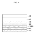
- FIG. 4 is a schematic cross-sectional view of the flexible display of FIG. 3 , and the substrate 200, the thin film transistor 300, and the organic light emitting element 400 are sequentially layered in the flexible display according to the exemplary embodiment.
- the substrate 200, the thin film transistor 300 (or thin film transistor layer), and the organic light emitting element 400 (or light emitting element layer) of FIG. 4 respectively correspond to the substrate 123, the driving thin film transistor 130, and the organic light emitting element LD of FIG. 3 .
- the thin film transistors layer 300 may be a layer including one or more thin film transistors of the flexible display.
- the light emitting layer 400 (or in other embodiments the light passage controlling elements layer) may be a layer that one or more light emitting elements (e.g. organic light emitting elements).
- the thin film transistors layer 300 and/or the light emitting elements layer 400 need not be continuous. Furthermore, in some embodiments, portions of the thin film transistors layer 300 and the light emitting elements layer 400 may be in the same plane.
- the substrate 200 includes the first support layer 210, the second support layer 250, and the heat-energy blocking/reflecting layer 230.
- the first support layer 210 and the second support layer 250 support the substrate 200, and form both side surfaces of the substrate 200. That is, as described above, the flexible substrate 200 is formed of dual support layers 210 and 250.
- the first support layer 210 and the second support layer 250 may be made of a polyimide having flexibility and an excellent heat resisting characteristic among polymers instead of a rigid material.
- the material of the first and second support layers 210 and 250 is not limited thereto in embodiments of the invention. Various materials having a flexible characteristic can be used in embodiments of the invention.
- the first support layer 210 may be formed below the thin film transistor 300, and the second support layer 250 may be disposed opposite to the first support layer 210 so as to have the heat-energy blocking/reflecting layer 230 interposed therebetween.
- the first support layer 210 and the second support layer 250 may be disposed at a distance from each other so as to interpose several layers therebetween.
- the heat-energy blocking/reflecting layer 230 is provided between the first support layer 210 and the second support layer 250.
- the heat-energy blocking/reflecting layer 230 blocks or reduces transmission of radiative heat energy (e.g., radiative energy in the InfraRed (IR) band of wavelengths) therethrough where the reflected and/or otherwise blocked heat-energy arises due to irradiation from below by laser beams applied to a lower portion of the carrier substrate 500 for the purpose of separating the carrier substrate 500 from the second support layer 250.
- radiative heat energy e.g., radiative energy in the InfraRed (IR) band of wavelengths
- the flexible display is manufactured by sequentially layering the substrate 200, the thin film transistor layer 300, and the organic light emitting elements layer 400 on a supporting carrier substrate 500 (e.g., a rigid carrier). Since the flexible display has flexibility, it is supported by a rigid substrate like that of the carrier substrate 500 during a manufacturing process.
- a supporting carrier substrate 500 e.g., a rigid carrier
- the heat-energy blocking/reflecting layer 230 is provided between the first support layer 210 and the second support layer 250 and is configured to block and/or reflect a sufficient amount of the heat energy to prevent irreversible damage to the organic light emitting elements layer 400 that might be caused by the heat energy.
- the heat-energy blocking/reflecting layer 230 may additionally prevent or impede permeation therethrough of moisture or oxygen into the flexible display to thereby help improve the reliability and/or usable lifetime of the flexible display.
- the reflective layer 230 may be made of an IR-reflecting and O2 impermeable metal film.
- the metallic heat-energy blocking/reflecting layer 230 can therefore reflect back the upwardly radiated heat energy that arises from the irradiation by the laser beam(s) in separating the second support layer 250 from the carrier substrate 500.
- the metal forming the heat-energy blocking/reflecting layer 230 may be aluminum (Al), chromium (Cr), molybdenum (Mo), alloys thereof and the like.
- the metal forming the heat-energy blocking/reflecting layer 230 is not limited thereto in embodiments of the invention, and various other metals having high reflectivity with respect to the spectrum of the radiated heat energy may be applicable in embodiments of the invention.
- a first insulating layer 220 is formed between the first support layer 210 and the heat-energy blocking/reflecting layer 230.
- a second insulating layer 240 is formed between the heat-energy blocking/reflecting layer 230 and the second support layer 250.
- the first insulating layer 220 and the second insulating layer 240 may be made of a silicon oxide (SiO x ) or a silicon nitride (SiN x ).
- a material forming the first and second support layers 210 and 250 is not limited thereto in embodiments of the invention, and various known materials that form an insulating layer used in a display may be applicable in embodiments of the invention.
- At least the first insulating layer 220 may be configured to impede thermal conduction therethrough.
- At least one of the first insulating layer 220 and the second insulating layer 240 may be further configured to prevent permeation of undesired impurities into the organic light emitting elements layer 400.
- the first insulating layer 220 and the second insulating layer 240 can block permeation of moisture or oxygen into the organic light emitting elements layer 400.
- the flexible display according to the exemplary embodiment can further effectively block permeation of moisture or oxygen into the organic light emitting element 400 by at least one of the first insulating layer 220 and the second insulating layer 240 while the heat-energy blocking/reflecting layer 230 blocks and/or reflects a sufficient amount of the heat energy to prevent irreversible damage to layers above itself.
- the substrate 200 may include only one of the first insulating layer 220 and the second insulating layer 240. That is, the substrate 200 may include only the first insulating layer 220 disposed between the first support layer 210 and the reflective layer 230 or only the second insulating layer 240 disposed between the reflective layer 230 and the second support layer 250. In other embodiments, the neither of the first insulating layer 220 or the second insulating layer 240 is present.
- the flexible display according to the exemplary embodiment can prevent damage to the organic light emitting elements layer 400 due to irradiation of laser beams in a manufacturing process by inclusion of the heat-energy blocking/reflecting layer, the first insulating layer, and the second insulating layer in the substrate, and can simultaneously prevent or impede permeation of moisture or oxygen into the organic light emitting element.
- photon blocking patterns are sometimes included in LCD displays for the purpose of blocking passage of visible light photons from their backlighting systems into the switching transistors that may be affected by such photons in the visible light portion of the spectrum.
- embodiments of the present invention contemplate the blockage and/or reflecting of photons in the InfraRed (IR) band of wavelengths and across substantially all portions of the display area, including those that constitute the light emitting and/or light valving aperture portions of the display area (DA) for the purpose of preventing or limiting irreversible damage to elements affected by such photons in the InfraRed (IR) band. It is also within the contemplation of the disclosure to block or reflect damaging photons in wavelength ranges above the visible range (above about 700nm, such as in the low UV range).
- the flexible display of some embodiments of the invention can use a light emitting elements layer (e.g. an organic emitting element).
- the light emitting elements layer could be replaced by a light passage controlling elements layer.
- a light passage controlling elements layer could, for example, comprise an LCD layer.
- Some embodiments of the invention provide a flexible display comprising a substrate, a thin film transistors layer formed on over the substrate, and a light emitting or light passage controlling elements layer formed on over the thin film transistors layer, wherein the substrate comprises: a first support layer formed below the thin film transistors layer; a second support layer disposed below the first support layer; and a heat-energy blocking/reflecting layer interposed between the first support layer and the second support layer.
- the thin film transistors layer may be a layer including one or more thin film transistors of the flexible display.
- the light emitting or light passage controlling elements layer may be a layer that includes at least one of an organic light emitting elements layer, a liquid crystal display elements layer, and an electrophoretic display elements layer.
- the light emitting or light passage controlling elements layer may comprise one or more light emitting elements (e.g. an organic light emitting element) or light controlling element (e.g. a liquid crystal display element).
- the thin film transistors layer and/or the light emitting or light passage controlling elements layer need not be continuous. Furthermore, in some embodiments, portions of the thin film transistors layer and the light emitting or light passage controlling elements layer may be in the same plane.
- some embodiments of the invention provide a flexible display comprising a substrate, a light emitting or light passage controlling elements layer formed over the substrate, wherein the substrate comprises: a first support layer formed below the light emitting or light passage controlling elements layer; a second support layer disposed below the first support layer; and a heat-energy blocking/reflecting layer interposed between the first support layer and the second support layer.
- some embodiments of the invention may use a thin film transistors layer that is above the light emitting or light passage controlling elements layer.
- Embodiments of the invention can also provide a method of manufacturing a flexible display device, the method comprising: adhering a base flexible substrate layer to a carrier substrate; disposing over the base flexible substrate layer a flexible heat-energy blocking/reflecting layer; disposing over the heat-energy blocking/reflecting layer a further layer of the flexible display device that can be damaged by exposure to an excessive amount of radiated heat-energy; and after disposing the further layer that can be damaged by exposure to said excessive amount of radiated heat-energy, separating the base flexible substrate layer from the carrier substrate by using a separation process that generates radiated heat-energy; wherein the heat-energy blocking/reflecting layer is configured to block or reflect a sufficient portion of the generated radiated heat-energy so as to prevent the damage to the further layer that can be damaged by exposure to said excessive amount of radiated heat-energy.
- the radiated heat-energy may result in the excessive amount of radiated heat-energy that damages the further layer.
- the method further comprises disposing over the heat-energy blocking/reflecting layer a second flexible substrate layer, wherein the heat-energy blocking/reflecting layer is interposed between the base flexible substrate layer and the second flexible substrate layer, wherein the further layer of the flexible display device that can be damaged by exposure to an excessive amount of radiated heat-energy is disposed above the second flexible substrate layer.
- the method further comprises forming at least one insulating layer between either the base flexible substrate layer and the heat-energy blocking/reflecting layer or between the heat-energy blocking/reflecting layer and the second flexible substrate layer.
Landscapes
- Engineering & Computer Science (AREA)
- Physics & Mathematics (AREA)
- Optics & Photonics (AREA)
- Manufacturing & Machinery (AREA)
- Microelectronics & Electronic Packaging (AREA)
- General Physics & Mathematics (AREA)
- Theoretical Computer Science (AREA)
- Geometry (AREA)
- Chemical & Material Sciences (AREA)
- Inorganic Chemistry (AREA)
- Electroluminescent Light Sources (AREA)
Abstract
Description
- The present disclosure relates to a flexible display and manufacture of the same.
- A flexible display that is light and strong and that uses a flexible plastic substrate has been recently developed. Such a flexible display can be folded or rolled in a roll-to-roll manner so that portability of the flexible display can be maximized and accordingly it can be applied to various fields.
- The flexible display includes a display element formed on a flexible substrate. A display element that can be used in the flexible display can be an organic light emitting diode (OLED) display element, a liquid crystal display element, an electrophoretic display (EPD) element, and the like.
- A flexible display uses a flexible material so that it can maintain display performance even through it is bent like paper. However, during mass production fabrication, such a flexible display is manufactured while being supported by and adhered to a rigid substrate, for example, a carrier substrate.
- When a process of layering several layers on the in-process flexible display is finished, the adhesions of the flexible substrate to its rigid support carrier is broken by, for example irradiating from the bottom with laser beams to thereby separate the flexible display from the carrier substrate. In this process, a light emission layer or another photon absorbing layer of the flexible display may be damaged due to receiving part of the irradiation of the substrates separating laser beam.
- It is to be understood that this background of the technology section is intended to provide useful background for understanding the here disclosed technology and as such, the technology background section may include ideas, concepts or recognitions that were not part of what was known or appreciated by those skilled in the pertinent art prior to corresponding invention dates of subject matter disclosed herein.
- A flexible display device is provided with a damage preventing layer that can prevent damage to an overlying light emission elements layer during mass production manufacture, where the damage can be due to irradiation by laser beams used to separate the in-process flexible display device from a supporting carrier substrate during the manufacturing process.
- A flexible display according to an exemplary embodiment includes a substrate, a thin film transistors layer formed on the substrate, and a light emitting elements layer formed on the thin film transistor, where the substrate layer includes a first support layer formed below the thin film transistors layer, a second support layer disposed below the first support layer, and a heat-energy blocking/reflecting layer provided between the first support layer and the second support layer.
- The flexible display may further include an insulating layer formed at least between the first support layer and the reflective layer or between the reflective layer and the second support layer.
- The first and/or second insulating layer may be made of a silicon oxide (SiOx) or a silicon nitride (SiNx).
- The heat-energy blocking/reflecting layer may be made of an IR light reflecting metal.
- The reflective layer may be predominantly composed of at least one of aluminum (Al), chromium (Cr), and molybdenum (Mo).
- The first support layer and the second support layer may be made of a polyimide.
- The light emitting elements layer may be one of an organic light emitting elements layer, a liquid crystal display elements layer, and an electrophoretic display elements layer.
- The flexible display according to the exemplary embodiment can prevent damage to the light emitting elements layer due to irradiation of laser beams in a manufacturing process, and can further, in one embodiment, effectively prevent or impede permeation therethrough of moisture or oxygen into the light emitting element after separation from the carrier substrate.
- According to an aspect of the invention, there is provided a flexible display comprising a substrate, a thin film transistors layer formed on the substrate, and a light emitting or light passage controlling elements layer formed on the thin film transistors layer, wherein the substrate comprises: a first support layer formed below the thin film transistors layer; a second support layer disposed below the first support layer; and a heat-energy blocking/reflecting layer interposed between the first support layer and the second support layer.
- According to an aspect of the invention, there is provided a method of manufacturing a flexible display device, the method comprising: adhering a base flexible substrate layer to and on a carrier substrate; disposing on the base flexible substrate layer, a flexible heat-energy blocking/reflecting layer; disposing above the heat-energy blocking/reflecting layer, a further layer of the flexible display device that can be damaged by exposure to an excessive amount of radiated heat-energy; and after disposing the further layer that can be damaged by exposure to said excessive amount of radiated heat-energy, separating the base flexible substrate layer from the carrier substrate by using a separation process that generates radiated heat-energy where the radiated heat-energy can result in the excessive amount of radiated heat-energy that damages the further layer that can be damaged by exposure to said excessive amount of radiated heat-energy; wherein the heat-energy blocking/reflecting layer is configured to block or reflect a sufficient portion of the generated radiated heat-energy so as to prevent the damage to the further layer that can be damaged by exposure to said excessive amount of radiated heat-energy.
- According to an aspect of the invention, there is provided a flexible display as set out in claim 1. Preferred features of this aspect are set out in claims 2 to 7.
- According to an aspect of the invention, there is provided a method of manufacturing a flexible display device as set out in claim 8. Preferred features of this aspect are set out in claims 9 to 15.
- Embodiments of the invention will now be described by way of example with reference to the accompanying drawings, in which:
-
FIG. 1 is a top plan view of a structure of a flexible display according to an exemplary embodiment. -
FIG. 2 is a circuit diagram of a pixel circuit of the flexible display ofFIG. 1 . -
FIG. 3 is a partially enlarged cross-sectional view of a thin film transistor and a light emission element used in the flexible display ofFIG. 1 . -
FIG. 4 is partially enlarged cross-sectional view of a part (i.e., a substrate) of the flexible display ofFIG. 3 . -
FIG. 5 andFIG. 6 show a process of separation of the flexible display according to the exemplary embodiment from the carrier substrate. - In the following detailed description, only certain exemplary embodiments in accordance with the present disclosure of invention have been shown and described, simply by way of illustration. As those skilled in the art would realize in light of this disclosure, the described embodiments may be modified in various different ways, all without departing from the spirit or scope of the present teachings. The drawings and description are to be regarded as illustrative in nature and not restrictive. Like reference numerals designate like elements throughout the specification.
- The size and thickness of the components shown in the drawings are optionally determined for better understanding and ease of description, and the present disclosure is not limited to the examples shown in the drawings.
- In the drawings, the thickness of layers, films, panels, regions, etc., are exaggerated for clarity. In addition, in the drawings, for better understanding and ease of description, the thickness of some layers and areas is exaggerated. It will be understood that when an element such as a layer, film, region, or substrate is referred to as being "on" another element, it can be directly on the other element or intervening elements may also be present.
- In addition, unless explicitly described to the contrary, the word "comprise" and variations such as "comprises" or "comprising" will be understood to imply the inclusion of stated elements but not the exclusion of any other elements. Further, it will be understood that when an element such as a layer, film, region, or substrate is referred to as being "on" another element, it can be directly on the other element or intervening elements may also be present.
- Referring to
FIG. 4 to FIG. 6 , a flexible display according to an exemplary embodiment has a structure that can prevent or reduce likelihood of damage to an irradiation sensitive layer, for example to an organic lightemitting elements layer 400 due to the use of laser beams for separation of in-process layers of the flexible display form a supporting carrier substrate (e.g., 500 ofFig. 5 ). The exemplary flexible display includes aflexible substrate 200, a thinfilm transistor layer 300, and the organic lightemitting elements layer 400. - The
substrate 200 includes afirst support layer 210, asecond support layer 250, and a photons blocking and/or reflective layer 230 (e.g., IR block/reflect layer 230). Details of thesubstrate 200 will be described in detail later. - First, referring to
FIG. 1 to FIG. 3 , an overview of the structure of the flexible display according to the exemplary embodiment will be described. - Referring to the top plan view of
FIG. 1 , aflexible display 101 according to the exemplary embodiment includes a substratemain body 111 divided into an image displaying area DA and a non-displaying area NA. Here, theflexible display 101 will be exemplarily illustrated as an organic light emission display formed of organic light emitting elements populating the display area (DA). However, the light emitting element of the flexible display is not limited thereto in embodiments of the invention, and a liquid crystal display element (e.g., a reflective kind), an electrophoretic display element, and the like may be used instead. - A plurality of pixel areas PX are formed in the display area DA of the substrate
main body 111 to display an image, and one or moredriving circuits driving circuits driving circuits - Referring to
FIG. 2 , theflexible display 101 according to the exemplary embodiment includes a plurality ofsignal lines signal lines - The signal lines include
scan lines 21 transmitting gate signals (or scan signals),data lines 71 transmitting data signals, anddriving voltage lines 72 transmitting driving voltages. Thescan signal lines 21 are substantially extended in a row direction and almost parallel with each other, and thedata lines 71 are substantially extended in a column direction and almost parallel with each other. Thedriving voltage lines 72 are substantially extended in the column direction, but they may be formed in a net shape rather than being extended in just one of the row or column direction. - Each pixel PX includes a switching transistor Qs, a driving transistor Qd, a storage capacitor Cst, and an organic light emitting element LD.
- The switching transistor Qs includes a control terminal N1, an input terminal N2, and an output terminal N3. The control terminal N1 is connected to the
scan signal line 21, the input terminal N2 is connected to thedata line 71, and the output terminal N3 is connected to the driving transistor Qd. The switching transistor Qs transmits a data signal received from thedata line 71 in response to the scan signal received from thescan signal line 21 to the driving transistor Qd. - The driving transistor Qd includes a control terminal N3, an input terminal N4, and an output terminal N5, and the control terminal N3 is connected to the switching transistor Qs, the input terminal N4 is connected to the
driving voltage line 72, and the output terminal N5 is connected to the organic light emitting element LD. The driving transistor Qd outputs an output current ILD whose magnitude varies according to a voltage applied between the control terminal N3 and the input terminal N4. - The capacitor Cst is connected between the control terminal N3 and the input terminal N4 of the driving transistor Qd. The capacitor Cst charges a data signal applied to the control terminal N3 of the driving transistor Qd and maintains charging of the data signal after the switching transistor Qs is turned off.
- The organic light emitting element LD is, for example, an organic light emitting diode (OLED), and includes an anode connected to the output terminal N5 of the driving transistor Qd and a cathode connected to a common voltage VSS. The organic light emitting element LD emits light by varying an intensity according to the output current ILD of the driving transistor Qd to display an image. The organic light emitting element LD may include an organic material which uniquely expresses any one or one or more of primary colors such as three primary colors of red, green, and blue, and the organic light emitting diode display displays a desired image by a spatial and/or temporal sum of the output colors.
- The switching transistor Qs and the driving transistor Qd are n-channel field effect transistors (FET), but at least one thereof may be a p-channel field effect transistor. Further, a connection relationship of the transistors Qs and Qd, the storage capacitor Cst, and the organic light emitting element LD may be changed.
- Such a configuration of the pixel area PX is not limited to the above in embodiments of the invention, and can be variously modified within the scope that can be easily modified by a person skilled in the art.
- Next, referring to
FIG. 3 , the cross sectional structure of the flexible display according to the exemplary embodiment will be described according to a layering order. Here, the structure of the driving transistor Qd and the organic light emitting element LD will be mainly described in detail. - A
substrate 123 is formed of a flexible substrate. Thesubstrate 123 has flexibility such that it can be used in the flexible display, and this will be described in detail later.
Abuffer layer 126 is formed on thesubstrate 123. Thebuffer layer 126 prevents permeation of an impurity (e.g., moisture and/or oxygen) and planarizes a surface.
In this case, thebuffer layer 126 may be made of various materials that can perform the above-stated functions. For example, thebuffer layer 126 may be formed of a single layer of one of a silicon nitride (SiNx), a silicon oxide (SiOx), and a silicon oxynitride (SiOxNy). However, thebuffer layer 126 may not be necessary, and may be omitted depending on the type and process conditions of thesubstrate 123.
A drivingsemiconductor layer 137 is formed on thebuffer layer 126. The drivingsemiconductor layer 137 is formed of a polysilicon layer. In addition, the drivingsemiconductor layer 137 includes achannel area 135 in which impurities are not doped and asource area 134 and adrain area 136 in which impurities are doped at respective sides of the channel area. In this case, implanted ion materials may be used as the dopant impurities and these may be a P-type impurity like boron B, and B2H6 is used in general. Here, such an impurity is changed depending on the type of the thin film transistor being formed. - A
gate insulating layer 127 formed of a silicon nitride (SiNx) or a silicon oxide (SiOx) is formed on the drivingsemiconductor layer 137. Gate wires including a drivinggate electrode 133 are formed on thegate insulating layer 127. In addition, the drivinggate electrode 133 overlaps at least a part of the drivingsemiconductor layer 137. - Particularly, the driving
gate electrode 133 overlaps thechannel area 135. - An interlayer insulating
layer 128 that covers the drivinggate electrode 133 is formed on thegate insulating layer 127. Through-holes that expose thesource area 134 and thedrain area 136 of the drivingsemiconductor layer 137 are respectively formed in thegate insulating layer 127 and the interlayer insulatinglayer 128. Like thegate insulating layer 127, theinterlayer insulating layer 128 may be made of a ceramic-based material such as a silicon nitride (SiNx) or a silicon oxide (SiOx). - Data wires including a driving
source electrode 131 and a drivingdrain electrode 132 are formed on theinterlayer insulating layer 128. In addition, the drivingsource electrode 131 and the drivingdrain electrode 132 are respectively connected with thesource area 134 and thedrain area 136 of the drivingsemiconductor layer 137 through the through-holes respectively formed in theinterlayer insulating layer 128 and thegate insulating layer 127. - As described, the driving
semiconductor layer 137, the drivinggate electrode 133, the drivingsource electrode 131, and the drivingdrain electrode 132 form a drivingthin film transistor 130. However, the configuration of the drivingthin film transistor 130 is not limited to the above-stated example in embodiments of the invention, and may have various known configurations that can be easily implemented by a person skilled in the art. - In addition, a
planarization layer 124 covering the data wires is formed on theinterlayer insulating layer 128. Theplanarization layer 124 removes a topographical step feature and planarizes a surface to improve light efficiency of an organic light emitting element to be formed thereon. In addition, theplanarization layer 124 includes anelectrode contact hole 122a that partially exposes thedrain electrode 132. Theplanarization layer 124 may be made of at least one of a polyacrylate resin, an epoxy resin, a phenolic resin, a polyamide resin, a polyimide resin, an unsaturated polyester resin, a polyphenylene ether resin, a polyphenylene sulfide resin, and benzocyclobutene (BCB). - Here, the exemplary embodiments are not limited to the above-stated structure, and one of the
planarization layer 124 and the interlayer insulatinglayer 128 may be omitted as necessary. - In this case, a first electrode of the organic light emitting element, that is, a
pixel electrode 122b, is formed on theplanarization layer 124. That is, the flexible display includes a plurality ofpixel electrodes 122b provided in each of the plurality of pixels. In this case, the plurality ofpixel electrodes 122b are separated from each other. Eachpixel electrode 122b is connected with arespective drain electrode 132 through the correspondingelectrode contact hole 122a of theplanarization layer 124. - A
pixel defining layer 125 having an opening that exposes thepixel electrode 122b is formed on theplanarization layer 124. That is, thepixel defining layer 125 includes a plurality of openings formed in each pixel. Anorganic emission layer 122c may be formed in each opening formed within thepixel defining layer 125. Accordingly, a pixel area where an organic emission layer is formed may be defined by thepixel defining layer 125. - In this case, the
pixel electrode 122b is disposed corresponding to the opening of thepixel defining layer 125, but this is not restrictive. That is, thepixel electrode 122b may be disposed below thepixel defining layer 125 such that a part of the pixel electrode 112b may be overlapped with thepixel defining layer 125. - The
pixel defining layer 125 may be made of a resin such as a polyacrylate resin, a polyimide resin, and the like, or a silica-based inorganic material. - The
organic emission layer 122c is formed on thepixel electrode 122b. Theorganic emission layer 122c may further include an emission layer (not shown) that substantially emits light in the visible range, and organic layers (not shown) for efficient transmission of carriers of holes or electrons to the emission layer. The organic layers may include a hole injection layer and a hole transport layer provided between thepixel electrode 122b and the emission layer and an electron injection layer and an electron transport layer provided between acommon electrode 122d and the emission layer. - In addition, a second electrode, that is, the
common electrode 122d, may be formed on theorganic emission layer 122c. As described, the organic light emitting element LD including thepixel electrode 122b, theorganic emission layer 122c, and thecommon electrode 122d is formed. - In this case, the
pixel electrode 122b and thecommon electrode 122d may be respectively made of a transparent conductive material or a semi-transmissive or reflective conductive material. Depending of the type of material forming thepixel electrode 122b and thecommon electrode 122d, the flexible display may be a front emission type of display, a bottom emission type of display, or a dual-side emissive type of display. - An
overcoat 190 that protects thecommon electrode 122d by covering the same may be formed as an organic layer on thecommon electrode 122d.
In addition, a thinfilm encapsulation layer 121 is formed on theovercoat 190. The thinfilm encapsulation layer 121 protects the organic light emitting element LD and the driving circuit formed in thesubstrate 123 by sealing them from the external environment. - The thin
film encapsulation layer 121 includesorganic encapsulation layers organic encapsulation layers FIG. 3 , twoorganic encapsulation layers film encapsulation layer 121, but this is not restrictive. -
FIG. 4 is a schematic cross-sectional view of the flexible display ofFIG. 3 , and thesubstrate 200, thethin film transistor 300, and the organiclight emitting element 400 are sequentially layered in the flexible display according to the exemplary embodiment. Here, thesubstrate 200, the thin film transistor 300 (or thin film transistor layer), and the organic light emitting element 400 (or light emitting element layer) ofFIG. 4 respectively correspond to thesubstrate 123, the drivingthin film transistor 130, and the organic light emitting element LD ofFIG. 3 . - The thin
film transistors layer 300 may be a layer including one or more thin film transistors of the flexible display.
The light emitting layer 400 (or in other embodiments the light passage controlling elements layer) may be a layer that one or more light emitting elements (e.g. organic light emitting elements). - It will be appreciated that, in some embodiments, the thin
film transistors layer 300 and/or the light emittingelements layer 400 need not be continuous. Furthermore, in some embodiments, portions of the thinfilm transistors layer 300 and the light emittingelements layer 400 may be in the same plane. - Referring to
FIG. 4 , thesubstrate 200 includes thefirst support layer 210, thesecond support layer 250, and the heat-energy blocking/reflectinglayer 230. - In this case, the
first support layer 210 and thesecond support layer 250 support thesubstrate 200, and form both side surfaces of thesubstrate 200. That is, as described above, theflexible substrate 200 is formed of dual support layers 210 and 250. - In this case, the
first support layer 210 and thesecond support layer 250 may be made of a polyimide having flexibility and an excellent heat resisting characteristic among polymers instead of a rigid material. However, the material of the first and second support layers 210 and 250 is not limited thereto in embodiments of the invention. Various materials having a flexible characteristic can be used in embodiments of the invention. - The
first support layer 210 may be formed below thethin film transistor 300, and thesecond support layer 250 may be disposed opposite to thefirst support layer 210 so as to have the heat-energy blocking/reflectinglayer 230 interposed therebetween. Thefirst support layer 210 and thesecond support layer 250 may be disposed at a distance from each other so as to interpose several layers therebetween. - Referring to
FIG. 4 to FIG. 6 , the heat-energy blocking/reflectinglayer 230 is provided between thefirst support layer 210 and thesecond support layer 250. The heat-energy blocking/reflectinglayer 230 blocks or reduces transmission of radiative heat energy (e.g., radiative energy in the InfraRed (IR) band of wavelengths) therethrough where the reflected and/or otherwise blocked heat-energy arises due to irradiation from below by laser beams applied to a lower portion of thecarrier substrate 500 for the purpose of separating thecarrier substrate 500 from thesecond support layer 250. - As shown in
FIG. 5 , the flexible display is manufactured by sequentially layering thesubstrate 200, the thinfilm transistor layer 300, and the organic light emittingelements layer 400 on a supporting carrier substrate 500 (e.g., a rigid carrier). Since the flexible display has flexibility, it is supported by a rigid substrate like that of thecarrier substrate 500 during a manufacturing process. - Referring to
FIG. 5 andFIG. 6 , when a process of layering layers that form the flexible display on thecarrier substrate 500 is finished, laser beams are irradiated to the lower portion of thecarrier substrate 500 to break down an adhesion mechanism that binds thesecond support layer 250 with thecarrier substrate 500 and to thereby separate thesubstrate 200 and thecarrier substrate 500. In this case, radiative heat energy in the form of photons in the InfraRed (IR) band of wavelengths is generated from the use of the laser beams and this radiative heat energy is transmitted into the flexible display. However, certain layers within the overlying and in-process flexible display 200-300-400 may be damaged by the upwardly transmitted radiative heat energy, for example the organic light emittingelements layer 400 may be damaged and/or otherwise undesirably influenced by the transmitted heat energy. - However, because the heat-energy blocking/reflecting
layer 230 is provided between thefirst support layer 210 and thesecond support layer 250 and is configured to block and/or reflect a sufficient amount of the heat energy to prevent irreversible damage to the organic light emittingelements layer 400 that might be caused by the heat energy. - Meanwhile, when formed of appropriate materials, the heat-energy blocking/reflecting
layer 230 may additionally prevent or impede permeation therethrough of moisture or oxygen into the flexible display to thereby help improve the reliability and/or usable lifetime of the flexible display. - According to the exemplary embodiment, the
reflective layer 230 may be made of an IR-reflecting and O2 impermeable metal film. The metallic heat-energy blocking/reflectinglayer 230 can therefore reflect back the upwardly radiated heat energy that arises from the irradiation by the laser beam(s) in separating thesecond support layer 250 from thecarrier substrate 500. - In this case, the metal forming the heat-energy blocking/reflecting
layer 230 may be aluminum (Al), chromium (Cr), molybdenum (Mo), alloys thereof and the like. However, the metal forming the heat-energy blocking/reflectinglayer 230 is not limited thereto in embodiments of the invention, and various other metals having high reflectivity with respect to the spectrum of the radiated heat energy may be applicable in embodiments of the invention. - Referring to
FIG. 4 , a first insulatinglayer 220 is formed between thefirst support layer 210 and the heat-energy blocking/reflectinglayer 230. In addition, a second insulatinglayer 240 is formed between the heat-energy blocking/reflectinglayer 230 and thesecond support layer 250. - In this case, the first insulating
layer 220 and the second insulatinglayer 240 may be made of a silicon oxide (SiOx) or a silicon nitride (SiNx). However, a material forming the first and second support layers 210 and 250 is not limited thereto in embodiments of the invention, and various known materials that form an insulating layer used in a display may be applicable in embodiments of the invention. At least the first insulatinglayer 220 may be configured to impede thermal conduction therethrough. - At least one of the first insulating
layer 220 and the second insulatinglayer 240 may be further configured to prevent permeation of undesired impurities into the organic light emittingelements layer 400. In further detail, the first insulatinglayer 220 and the second insulatinglayer 240 can block permeation of moisture or oxygen into the organic light emittingelements layer 400. - Thus, the flexible display according to the exemplary embodiment can further effectively block permeation of moisture or oxygen into the organic
light emitting element 400 by at least one of the first insulatinglayer 220 and the second insulatinglayer 240 while the heat-energy blocking/reflectinglayer 230 blocks and/or reflects a sufficient amount of the heat energy to prevent irreversible damage to layers above itself. - Meanwhile, according to another exemplary embodiment, the
substrate 200 may include only one of the first insulatinglayer 220 and the second insulatinglayer 240. That is, thesubstrate 200 may include only the first insulatinglayer 220 disposed between thefirst support layer 210 and thereflective layer 230 or only the second insulatinglayer 240 disposed between thereflective layer 230 and thesecond support layer 250. In other embodiments, the neither of the first insulatinglayer 220 or the second insulatinglayer 240 is present. - The flexible display according to the exemplary embodiment can prevent damage to the organic light emitting
elements layer 400 due to irradiation of laser beams in a manufacturing process by inclusion of the heat-energy blocking/reflecting layer, the first insulating layer, and the second insulating layer in the substrate, and can simultaneously prevent or impede permeation of moisture or oxygen into the organic light emitting element. - It is to be noted that photon blocking patterns are sometimes included in LCD displays for the purpose of blocking passage of visible light photons from their backlighting systems into the switching transistors that may be affected by such photons in the visible light portion of the spectrum. However, embodiments of the present invention contemplate the blockage and/or reflecting of photons in the InfraRed (IR) band of wavelengths and across substantially all portions of the display area, including those that constitute the light emitting and/or light valving aperture portions of the display area (DA) for the purpose of preventing or limiting irreversible damage to elements affected by such photons in the InfraRed (IR) band. It is also within the contemplation of the disclosure to block or reflect damaging photons in wavelength ranges above the visible range (above about 700nm, such as in the low UV range).
- As discussed, the flexible display of some embodiments of the invention can use a light emitting elements layer (e.g. an organic emitting element). In other embodiments, the light emitting elements layer could be replaced by a light passage controlling elements layer. Such a light passage controlling elements layer could, for example, comprise an LCD layer.
- Some embodiments of the invention provide a flexible display comprising a substrate, a thin film transistors layer formed on over the substrate, and a light emitting or light passage controlling elements layer formed on over the thin film transistors layer, wherein the substrate comprises: a first support layer formed below the thin film transistors layer; a second support layer disposed below the first support layer; and a heat-energy blocking/reflecting layer interposed between the first support layer and the second support layer.
- The thin film transistors layer may be a layer including one or more thin film transistors of the flexible display.
- The light emitting or light passage controlling elements layer may be a layer that includes at least one of an organic light emitting elements layer, a liquid crystal display elements layer, and an electrophoretic display elements layer. In other words, the light emitting or light passage controlling elements layer may comprise one or more light emitting elements (e.g. an organic light emitting element) or light controlling element (e.g. a liquid crystal display element).
- It will be appreciated that the thin film transistors layer and/or the light emitting or light passage controlling elements layer need not be continuous. Furthermore, in some embodiments, portions of the thin film transistors layer and the light emitting or light passage controlling elements layer may be in the same plane.
- It will also be appreciated that embodiments of the invention could be used for passive devices. Hence, some embodiments of the invention provide a flexible display comprising a substrate, a light emitting or light passage controlling elements layer formed over the substrate, wherein the substrate comprises: a first support layer formed below the light emitting or light passage controlling elements layer; a second support layer disposed below the first support layer; and a heat-energy blocking/reflecting layer interposed between the first support layer and the second support layer.
- In addition, some embodiments of the invention may use a thin film transistors layer that is above the light emitting or light passage controlling elements layer.
- Embodiments of the invention can also provide a method of manufacturing a flexible display device, the method comprising: adhering a base flexible substrate layer to a carrier substrate; disposing over the base flexible substrate layer a flexible heat-energy blocking/reflecting layer; disposing over the heat-energy blocking/reflecting layer a further layer of the flexible display device that can be damaged by exposure to an excessive amount of radiated heat-energy; and after disposing the further layer that can be damaged by exposure to said excessive amount of radiated heat-energy, separating the base flexible substrate layer from the carrier substrate by using a separation process that generates radiated heat-energy; wherein the heat-energy blocking/reflecting layer is configured to block or reflect a sufficient portion of the generated radiated heat-energy so as to prevent the damage to the further layer that can be damaged by exposure to said excessive amount of radiated heat-energy.
- In such embodiments, without the presence of the heat-energy blocking/reflecting layer, the radiated heat-energy may result in the excessive amount of radiated heat-energy that damages the further layer.
- In some embodiments, the method further comprises disposing over the heat-energy blocking/reflecting layer a second flexible substrate layer, wherein the heat-energy blocking/reflecting layer is interposed between the base flexible substrate layer and the second flexible substrate layer, wherein the further layer of the flexible display device that can be damaged by exposure to an excessive amount of radiated heat-energy is disposed above the second flexible substrate layer.
- In some embodiments, the method further comprises forming at least one insulating layer between either the base flexible substrate layer and the heat-energy blocking/reflecting layer or between the heat-energy blocking/reflecting layer and the second flexible substrate layer.
- While this disclosure of invention has been described in connection with what is presently considered to be practical exemplary embodiments, it is to be understood that the present teachings are not limited to the disclosed embodiments, but, on the contrary, they intended to cover various modifications and equivalent arrangements included within the scope of the present teachings.
Claims (15)
- A flexible display comprising a substrate, light emitting or light passage controlling elements formed over the substrate, wherein the substrate comprises:a first support layer formed below the light emitting or light passage controlling elements;a second support layer disposed below the first support layer; anda heat-energy blocking/reflecting layer interposed between the first support layer and the second support layer.
- The flexible display of Claim 1, further comprising thin film transistors formed over the substrate, optionally wherein the thin film transistors are interposed between the first support layer and the light emitting or light passage controlling elements.
- The flexible display of Claim 1 or 2, further comprising at least one insulating layer formed between either the first support layer and the heat-energy blocking/reflecting layer or between the heat-energy blocking/reflecting layer and the second support layer;
optionally wherein the at least one insulating layer includes a silicon oxide (SiOx) or a silicon nitride (SiNx). - The flexible display of any one of Claims 1 to 3, wherein the heat-energy blocking/reflecting layer is made of a metal.
- The flexible display of Claim 4, wherein the heat-energy blocking/reflecting layer is predominantly made of at least one of aluminum (Al), chromium (Cr), and molybdenum (Mo).
- The flexible display of any one of Claims 1 to 5, wherein the first support layer and the second support layer are each made of a polyimide.
- The flexible display of any one of Claims 1 to 6, wherein the light emitting or light passage controlling elements layer is at least one of an organic light emitting elements layer, a liquid crystal display elements layer, and an electrophoretic display elements layer.
- A method of manufacturing a flexible display device, the method comprising:adhering a base flexible substrate layer to a carrier substrate;disposing over the base flexible substrate layer, a flexible heat-energy blocking/reflecting layer;disposing over the heat-energy blocking/reflecting layer, a further layer of the flexible display device that can be damaged by exposure to an excessive amount of radiated heat-energy; andafter disposing the further layer that can be damaged by exposure to said excessive amount of radiated heat-energy, separating the base flexible substrate layer from the carrier substrate by using a separation process that generates radiated heat-energy;wherein the heat-energy blocking/reflecting layer is configured to block or reflect a sufficient portion of the generated radiated heat-energy so as to prevent the damage to the further layer that can be damaged by exposure to said excessive amount of radiated heat-energy.
- The method of Claim 8 wherein:the heat-energy blocking/reflecting layer is configured to block or reflect damaging photons in wavelength ranges below or above the visible range.
- The method of Claim 9 wherein:the heat-energy blocking/reflecting layer includes a metal that reflects IR photons.
- The method of Claim 10 wherein:the heat-energy blocking/reflecting layer includes or is attached to a material that prevents or impedes substantial permeation of moisture and/or oxygen therethrough.
- The method of any one of Claims 8 to 11 wherein:the further layer that can be damaged by exposure to said excessive amount of radiated heat-energy is a light emitting and/or a selective light passage controlling layer of the flexible display device.
- The method of Claim 12 wherein:the further layer that can be damaged by exposure to said excessive amount of radiated heat-energy includes organic light emitting elements.
- The method of Claim 13 wherein:the organic light emitting elements can be damaged by exposure to moisture and/or oxygen; andthe heat-energy blocking/reflecting layer includes or is attached to a material that prevents or impedes substantial permeation of moisture and/or oxygen therethrough.
- The method of any one of Claims 8 to 14, further comprising disposing over the heat-energy blocking/reflecting layer a second flexible substrate layer, wherein the heat-energy blocking/reflecting layer is interposed between the base flexible substrate layer and the second flexible substrate layer, wherein the further layer of the flexible display device that can be damaged by exposure to an excessive amount of radiated heat-energy is disposed above the second flexible substrate layer;
optionally wherein the method further comprises forming at least one insulating layer between either the base flexible substrate layer and the heat-energy blocking/reflecting layer or between the heat-energy blocking/reflecting layer and the second flexible substrate layer.
Applications Claiming Priority (1)
| Application Number | Priority Date | Filing Date | Title |
|---|---|---|---|
| KR1020130094272A KR102100763B1 (en) | 2013-08-08 | 2013-08-08 | Flexible display device |
Publications (1)
| Publication Number | Publication Date |
|---|---|
| EP2849239A1 true EP2849239A1 (en) | 2015-03-18 |
Family
ID=51266240
Family Applications (1)
| Application Number | Title | Priority Date | Filing Date |
|---|---|---|---|
| EP20140180267 Ceased EP2849239A1 (en) | 2013-08-08 | 2014-08-07 | Flexible display having damage impeding layer and method for manufacturing the same |
Country Status (3)
| Country | Link |
|---|---|
| US (2) | US9653481B2 (en) |
| EP (1) | EP2849239A1 (en) |
| KR (1) | KR102100763B1 (en) |
Families Citing this family (15)
| Publication number | Priority date | Publication date | Assignee | Title |
|---|---|---|---|---|
| JP2014186169A (en) * | 2013-03-22 | 2014-10-02 | Toshiba Corp | Manufacturing method of display device and display device |
| JP6495754B2 (en) * | 2015-06-12 | 2019-04-03 | 株式会社ジャパンディスプレイ | Display device |
| WO2017007494A1 (en) * | 2015-07-09 | 2017-01-12 | Hewlett-Packard Development Company, L.P. | Flexible display |
| US10818652B2 (en) * | 2016-07-15 | 2020-10-27 | Samsung Display Co., Ltd. | Display device and manufacturing method thereof |
| US10312461B2 (en) | 2017-10-30 | 2019-06-04 | Wuhan China Star Optoelectronics Semiconductor Display Technology Co., Ltd. | Flexible OLED display panel having a substrate with a titanium layer and method for manufacturing same |
| CN107623087A (en) * | 2017-10-30 | 2018-01-23 | 武汉华星光电半导体显示技术有限公司 | Flexible OLED display panel and preparation method thereof |
| KR102505255B1 (en) * | 2017-12-26 | 2023-02-28 | 엘지디스플레이 주식회사 | Display apparatus |
| JP6666530B2 (en) * | 2018-03-20 | 2020-03-13 | 堺ディスプレイプロダクト株式会社 | Flexible OLED device, method of manufacturing the same, and support substrate |
| KR102602157B1 (en) | 2018-06-29 | 2023-11-14 | 삼성디스플레이 주식회사 | Organic light-emitting display device and method of manufacturing the same |
| CN110473981A (en) | 2019-07-30 | 2019-11-19 | 武汉华星光电半导体显示技术有限公司 | A kind of display panel and preparation method thereof |
| KR102814722B1 (en) * | 2019-10-29 | 2025-05-30 | 삼성디스플레이 주식회사 | Display apparatus |
| WO2021102664A1 (en) * | 2019-11-26 | 2021-06-03 | 重庆康佳光电技术研究院有限公司 | Display assembly and electronic device using display assembly |
| JP6851519B2 (en) * | 2020-02-20 | 2021-03-31 | 堺ディスプレイプロダクト株式会社 | Flexible OLED device, its manufacturing method, and support substrate |
| CN112562519B (en) * | 2020-12-28 | 2023-01-06 | 湖北长江新型显示产业创新中心有限公司 | Foldable display device |
| KR20230102594A (en) * | 2021-12-30 | 2023-07-07 | 엘지디스플레이 주식회사 | Display device |
Citations (7)
| Publication number | Priority date | Publication date | Assignee | Title |
|---|---|---|---|---|
| US20030197197A1 (en) * | 2002-04-12 | 2003-10-23 | Brown Julia J. | Organic electronic devices with pressure sensitive adhesive layer |
| US20040046496A1 (en) * | 2002-08-14 | 2004-03-11 | Masayuki Mishima | Light-emitting device and its production |
| WO2005064993A1 (en) * | 2003-12-30 | 2005-07-14 | Agency For Science, Technology And Research | Flexible electroluminescent devices |
| KR20080004232A (en) * | 2006-07-05 | 2008-01-09 | 삼성에스디아이 주식회사 | Manufacturing method of thin film transistor stuck substrate and manufacturing method of organic light emitting display device using same |
| US20110032223A1 (en) * | 2009-08-07 | 2011-02-10 | Semiconductor Energy Laboratory Co., Ltd. | Display Panel and Electronic Book |
| US20120007083A1 (en) * | 2010-07-07 | 2012-01-12 | Samsung Mobile Display Co., Ltd. | Organic light-emitting display device and manufacturing method of the same |
| US20120187399A1 (en) * | 2009-09-30 | 2012-07-26 | Dai Nippon Printing Co., Ltd. | Substrate for flexible device, thin film transistor substrate for flexible device, flexible device, substrate for thin film element, thin film element, thin film transistor, method for manufacturing substrate for thin film element, method for manufacturing thin film element, and method for manufacturing thin film transistor |
Family Cites Families (3)
| Publication number | Priority date | Publication date | Assignee | Title |
|---|---|---|---|---|
| JP2008107510A (en) * | 2006-10-25 | 2008-05-08 | Nitto Denko Corp | Display element substrate and manufacturing method thereof |
| KR100902928B1 (en) | 2007-12-06 | 2009-06-15 | 엘지전자 주식회사 | Flexible film, display device including same, and manufacturing method of display device |
| KR20120077473A (en) | 2010-12-30 | 2012-07-10 | 삼성모바일디스플레이주식회사 | Flexible substrate and display device including the same |
-
2013
- 2013-08-08 KR KR1020130094272A patent/KR102100763B1/en not_active Expired - Fee Related
-
2014
- 2014-06-02 US US14/293,947 patent/US9653481B2/en not_active Expired - Fee Related
- 2014-08-07 EP EP20140180267 patent/EP2849239A1/en not_active Ceased
-
2017
- 2017-04-18 US US15/490,192 patent/US20170222192A1/en not_active Abandoned
Patent Citations (7)
| Publication number | Priority date | Publication date | Assignee | Title |
|---|---|---|---|---|
| US20030197197A1 (en) * | 2002-04-12 | 2003-10-23 | Brown Julia J. | Organic electronic devices with pressure sensitive adhesive layer |
| US20040046496A1 (en) * | 2002-08-14 | 2004-03-11 | Masayuki Mishima | Light-emitting device and its production |
| WO2005064993A1 (en) * | 2003-12-30 | 2005-07-14 | Agency For Science, Technology And Research | Flexible electroluminescent devices |
| KR20080004232A (en) * | 2006-07-05 | 2008-01-09 | 삼성에스디아이 주식회사 | Manufacturing method of thin film transistor stuck substrate and manufacturing method of organic light emitting display device using same |
| US20110032223A1 (en) * | 2009-08-07 | 2011-02-10 | Semiconductor Energy Laboratory Co., Ltd. | Display Panel and Electronic Book |
| US20120187399A1 (en) * | 2009-09-30 | 2012-07-26 | Dai Nippon Printing Co., Ltd. | Substrate for flexible device, thin film transistor substrate for flexible device, flexible device, substrate for thin film element, thin film element, thin film transistor, method for manufacturing substrate for thin film element, method for manufacturing thin film element, and method for manufacturing thin film transistor |
| US20120007083A1 (en) * | 2010-07-07 | 2012-01-12 | Samsung Mobile Display Co., Ltd. | Organic light-emitting display device and manufacturing method of the same |
Also Published As
| Publication number | Publication date |
|---|---|
| KR20150018680A (en) | 2015-02-24 |
| US20170222192A1 (en) | 2017-08-03 |
| KR102100763B1 (en) | 2020-04-16 |
| US20150042913A1 (en) | 2015-02-12 |
| US9653481B2 (en) | 2017-05-16 |
Similar Documents
| Publication | Publication Date | Title |
|---|---|---|
| US9653481B2 (en) | Flexible display having damage impeding layer and method for manufacturing the same | |
| US11818924B2 (en) | Flexible organic electroluminescent device and method for fabricating the same | |
| KR102749163B1 (en) | Display device and manufacturing method thereof | |
| US9525015B2 (en) | Organic light emitting diode device and method for fabricating the same | |
| US10134826B2 (en) | Display apparatus including detour lines | |
| JP6286941B2 (en) | LIGHT EMITTING DEVICE, LIGHT EMITTING DEVICE MANUFACTURING METHOD, ELECTRONIC DEVICE | |
| US8227803B2 (en) | Organic electroluminescent display device and method for fabricating the same | |
| US7893899B2 (en) | Organic light emitting diode display and fabricating method thereof | |
| US9190629B2 (en) | Flexible organic electroluminescent device and method for fabricating the same | |
| KR102740803B1 (en) | Organic light emitting display device | |
| KR20160043327A (en) | Organic light emitting display | |
| CN101324306A (en) | Light-emitting diode arrays and methods of manufacture | |
| KR102554738B1 (en) | Organic light emitting diode device and favricating method thereof | |
| KR102016070B1 (en) | Flexible organic luminescence emitted diode device and method for fabricating the same | |
| KR102717480B1 (en) | Organic light emitting display device | |
| US20130063022A1 (en) | Organic Light Emitting Diode Display | |
| KR102141558B1 (en) | Flexible organic electroluminescent emitted diode device and method for fabricating the same | |
| EP3525064B1 (en) | Display device and method for fabricating the same | |
| KR102167046B1 (en) | Display apparatus | |
| KR102381901B1 (en) | Display device and manufacturing method thereof | |
| KR102598743B1 (en) | Organic light emitting display device and method for fabricating the same | |
| KR102467218B1 (en) | Display device and method for fabricating the same | |
| US20240213419A1 (en) | Display device | |
| KR102455579B1 (en) | Organic light emitting display device and method for fabricating the same | |
| US20250268092A1 (en) | Display device |
Legal Events
| Date | Code | Title | Description |
|---|---|---|---|
| PUAI | Public reference made under article 153(3) epc to a published international application that has entered the european phase |
Free format text: ORIGINAL CODE: 0009012 |
|
| 17P | Request for examination filed |
Effective date: 20140807 |
|
| AK | Designated contracting states |
Kind code of ref document: A1 Designated state(s): AL AT BE BG CH CY CZ DE DK EE ES FI FR GB GR HR HU IE IS IT LI LT LU LV MC MK MT NL NO PL PT RO RS SE SI SK SM TR |
|
| AX | Request for extension of the european patent |
Extension state: BA ME |
|
| RAP1 | Party data changed (applicant data changed or rights of an application transferred) |
Owner name: SAMSUNG DISPLAY CO., LTD. |
|
| R17P | Request for examination filed (corrected) |
Effective date: 20150918 |
|
| RBV | Designated contracting states (corrected) |
Designated state(s): AL AT BE BG CH CY CZ DE DK EE ES FI FR GB GR HR HU IE IS IT LI LT LU LV MC MK MT NL NO PL PT RO RS SE SI SK SM TR |
|
| STAA | Information on the status of an ep patent application or granted ep patent |
Free format text: STATUS: EXAMINATION IS IN PROGRESS |
|
| 17Q | First examination report despatched |
Effective date: 20190227 |
|
| STAA | Information on the status of an ep patent application or granted ep patent |
Free format text: STATUS: THE APPLICATION HAS BEEN REFUSED |
|
| 18R | Application refused |
Effective date: 20210921 |