EP2849005A1 - Standby dual redundant system - Google Patents
Standby dual redundant system Download PDFInfo
- Publication number
- EP2849005A1 EP2849005A1 EP12876411.5A EP12876411A EP2849005A1 EP 2849005 A1 EP2849005 A1 EP 2849005A1 EP 12876411 A EP12876411 A EP 12876411A EP 2849005 A1 EP2849005 A1 EP 2849005A1
- Authority
- EP
- European Patent Office
- Prior art keywords
- data
- standby
- side controller
- cpu
- equalization
- Prior art date
- Legal status (The legal status is an assumption and is not a legal conclusion. Google has not performed a legal analysis and makes no representation as to the accuracy of the status listed.)
- Granted
Links
Images


Classifications
-
- G—PHYSICS
- G05—CONTROLLING; REGULATING
- G05B—CONTROL OR REGULATING SYSTEMS IN GENERAL; FUNCTIONAL ELEMENTS OF SUCH SYSTEMS; MONITORING OR TESTING ARRANGEMENTS FOR SUCH SYSTEMS OR ELEMENTS
- G05B9/00—Safety arrangements
- G05B9/02—Safety arrangements electric
- G05B9/03—Safety arrangements electric with multiple-channel loop, i.e. redundant control systems
-
- G—PHYSICS
- G06—COMPUTING; CALCULATING OR COUNTING
- G06F—ELECTRIC DIGITAL DATA PROCESSING
- G06F11/00—Error detection; Error correction; Monitoring
- G06F11/07—Responding to the occurrence of a fault, e.g. fault tolerance
- G06F11/16—Error detection or correction of the data by redundancy in hardware
- G06F11/20—Error detection or correction of the data by redundancy in hardware using active fault-masking, e.g. by switching out faulty elements or by switching in spare elements
- G06F11/202—Error detection or correction of the data by redundancy in hardware using active fault-masking, e.g. by switching out faulty elements or by switching in spare elements where processing functionality is redundant
- G06F11/2023—Failover techniques
- G06F11/2028—Failover techniques eliminating a faulty processor or activating a spare
-
- G—PHYSICS
- G06—COMPUTING; CALCULATING OR COUNTING
- G06F—ELECTRIC DIGITAL DATA PROCESSING
- G06F11/00—Error detection; Error correction; Monitoring
- G06F11/07—Responding to the occurrence of a fault, e.g. fault tolerance
- G06F11/16—Error detection or correction of the data by redundancy in hardware
- G06F11/20—Error detection or correction of the data by redundancy in hardware using active fault-masking, e.g. by switching out faulty elements or by switching in spare elements
- G06F11/2097—Error detection or correction of the data by redundancy in hardware using active fault-masking, e.g. by switching out faulty elements or by switching in spare elements maintaining the standby controller/processing unit updated
-
- G—PHYSICS
- G05—CONTROLLING; REGULATING
- G05B—CONTROL OR REGULATING SYSTEMS IN GENERAL; FUNCTIONAL ELEMENTS OF SUCH SYSTEMS; MONITORING OR TESTING ARRANGEMENTS FOR SUCH SYSTEMS OR ELEMENTS
- G05B2219/00—Program-control systems
- G05B2219/20—Pc systems
- G05B2219/24—Pc safety
- G05B2219/24186—Redundant processors are synchronised
-
- G—PHYSICS
- G05—CONTROLLING; REGULATING
- G05B—CONTROL OR REGULATING SYSTEMS IN GENERAL; FUNCTIONAL ELEMENTS OF SUCH SYSTEMS; MONITORING OR TESTING ARRANGEMENTS FOR SUCH SYSTEMS OR ELEMENTS
- G05B2219/00—Program-control systems
- G05B2219/20—Pc systems
- G05B2219/24—Pc safety
- G05B2219/24187—Redundant processors run identical programs
-
- G—PHYSICS
- G05—CONTROLLING; REGULATING
- G05B—CONTROL OR REGULATING SYSTEMS IN GENERAL; FUNCTIONAL ELEMENTS OF SUCH SYSTEMS; MONITORING OR TESTING ARRANGEMENTS FOR SUCH SYSTEMS OR ELEMENTS
- G05B2219/00—Program-control systems
- G05B2219/20—Pc systems
- G05B2219/24—Pc safety
- G05B2219/24195—Compare data in channels at timed intervals, for equality
Definitions
- the present invention relates to a standby dual redundant system with dual controllers each having multiple CPUs to perform different calculations by the respective CPUs in a constant cycle.
- the CPUs have respective system bus controllers, and each CPU is connected to a system bus via the system bus controller.
- a standby dual redundant system as shown in Patent Document 1 is proposed.
- equalization data is transmitted from an active-side CPU to a standby-side CPU by using the system bus controller, thereby realizing data equalization between the two controllers.
- Patent Document 1 Japanese Laid-Open Patent Publication JP-A-2002-149 212 (paragraphs [0020] to [0022], FIG. 1 , FIG. 3 )
- a bus is provided for transferring data to be equalized from an active-side CPU to a standby-side CPU.
- the equalization controller shown in Patent Document 1 since each CPU has the bus controller for equalizing data, if the number of the CPUs increases, the same number of bus controllers as the increased CPUs are required.
- transmission/reception of equalization data and transmission/reception of data with an I/O board use the same system bus. Therefore, transmission/reception of equalization data and transmission/reception with the I/O board cannot be performed simultaneously, and thus there is a problem that response of data transfer cannot be improved.
- the present invention has been made to solve the above problems, and an object of the present invention is to provide a standby dual redundant system that can suppress the circuit scale without increasing the number of bus controllers even if the number of CPUs increases, and allows simultaneous execution of transmission/reception of equalization data between controllers and transmission/reception of data between an I/O board and a CPU.
- a standby dual redundant system includes two controllers such that, when one of the controllers operates as an active-side controller, the other controller operates as a standby-side controller, each controller having therein: a plurality of CPUs; a memory; an I/O board; an I/O bus controller for performing transmission and reception of data among the plurality of CPUs, the memory, and the I/O board; and an equalization bus controller for transmitting equalization data used for equalizing device states of the active-side controller and the standby-side controller, from the active-side controller to the standby-side controller via an equalization data bus, the equalization bus controller being independent from the I/O bus controller.
- each controller has therein: a plurality of CPUs; a memory; an I/O board; an I/O bus controller for performing transmission and reception of data among the plurality of CPUs, the memory, and the I/O board; and an equalization bus controller for transmitting equalization data used for equalizing device states of the active-side controller and the standby-side controller, from the active-side controller to the standby-side controller via an equalization data bus, the equalization bus controller being independent from the I/O bus controller.
- equalization data bus and the I/O bus are configured as independent buses, and their respective bus controllers are also independent from each other, it becomes possible to perform transmission/reception of equalization data and transmission/reception with the I/O board simultaneously, thus realizing high-speed processing.
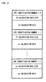
- FIG. 1 is a diagram showing the configuration of a standby dual redundant system 100 (hereinafter, referred to as a system 100).
- the system 100 includes an active-side controller 10a, a standby-side controller 10b, and an equalization data bus 20.
- a calculation result of the active-side controller 10a is sent to the standby-side controller 10b via the equalization data bus 20.
- the standby-side controller 10b has the same configuration as the active-side controller 10a. Therefore, the configuration of each controller will be described based on, mainly, the active-side controller 10a.
- the active-side controller 10a includes a CPU board 1a, a plurality of I/O boards 2a, and an I/O bus 3a. Input data needed for a calculation routine of the CPU board 1a is obtained by being read from the I/O board 2a via the I/O bus 3a.
- output data that is a calculation result of the calculation routine of the CPU board 1a is written into the I/O board 2a via the I/O bus 3a.
- Output of data to a device controlled by the system 100 is performed by the I/O board 2a in the active-side controller 10a.
- the CPU board 1a includes a plurality of CPUs from a CPU a0 to a CPU an, a memory 11a, an equalization bus controller 12a, an I/O bus controller 13a, an interruption control 14a which corresponds to an execution control section in claims, and a timer 15 a.
- the plurality of CPUs from the CPU a0 to the CPU an perform respective different calculations.
- the I/O bus controller 13a performs data transmission between the memory 11a and the plurality of I/O boards 2a via the I/O bus 3a in accordance with a reading request or a writing request for data to be used by each CPU.
- the equalization bus controller 12a of the active-side controller 10a transmits a result of calculation performed by each CPU of the active-side controller 10a, or the like, to an equalization bus controller 12b of the standby-side controller 10b via the equalization data bus 20.
- the equalization bus controller 12b of the standby-side controller 10b stores the received data into a memory 11b of the standby-side controller 10b.
- the interruption control 14a notifies each of the CPUs a0 to an of interruption, using an interruption signal bus 16a.
- timer 15a is connected to the interruption control 14a, whereby a predetermined CPU can be notified of interruption at regular intervals.
- FIG. 2 is a diagram showing the configuration of the interruption control 14a.
- the interruption control 14a is provided with respective interruption notification registers for the CPUs a0 to an. For example, when data is set in the interruption notification register for CPU a0, an interruption signal 17a0 to the CPU a0 is turned on, whereby the CPU a0 is notified of interruption.
- the interruption notification registers and the interruption signals 17a0 to 17an are provided for the respective CPUs.
- the interruption notification registers for the CPUs a0 to an are accessible from each other's CPU, and each CPU can notify another CPU of interruption.
- FIG. 3 is a diagram showing the configuration of data stored in the memory 11a and the memory 11b.
- the memory 11a and the memory 11b have the same configuration. Therefore, the memory 11a will be described.
- Input data 11a1 is data obtained by being read from the I/O board 2a.
- Output data 11a2 is data to be written into the I/O board 2a.
- the input data 11a1 and the output data 11a2 are stored in a format used in transmission and reception between the I/O board 2a and a control target device.
- calculation routines p0 to pn are stored, which are performed by the CPUs a0 to an, respectively.
- the calculation routines p0 to pn each include processing (calculation 1) of converting, from the input data 11a1, data to be used in calculation by each CPU into a format suitable for the calculation, processing (calculation 2) of actually performing the calculation, and processing (calculation 3) of converting the calculation result into a data format suitable for output from the I/O board 2a.
- data for calculation used in the calculation routines p0 to pn performed by the CPUs a0 to an are arranged in the order from calculation data pd0 to calculation data pdn for the respective CPUs.
- the calculation data pd0 is actually composed of a plurality of data.
- the first type of data is data obtained by acquiring data to be used in the calculation routine p0 for CPU a0 from the input data 11a1 and then converting the data into a format suitable for the calculation 2 by the calculation 1 in the calculation routine p0.
- the second type of data is composed of data obtained as a result of the calculation 2 in the calculation routine p0 and an accumulated data group of such data in the past.
- the third type of data is data obtained by converting the resultant data of the calculation 2 in the calculation routine p0 into a format of output data to the I/O board 2a by the calculation 3 in the calculation routine p0.
- the memory 11a has an equalization data transmission buffer 11a3, an equalization data reception buffer 11a4, and an equalization data reception buffer 11a5.
- the equalization data transmission buffer 11a3 is used when the controller operates as the active-side controller 10a.
- the equalization bus controller 12a of the active-side controller 10a transmits a content of the equalization data transmission buffer 11a3 to the equalization bus controller 12b of the standby-side controller 10b.
- the equalization bus controller 12a adds a checksum used for confirmation of the validity of the transmitted data.
- the equalization data reception buffer 11a4 and the equalization data reception buffer 11a5 are used when the controller operates as the standby-side controller.
- the equalization bus controller 12b of the standby-side controller 10b confirms data received from the active-side controller 10a, by using a checksum.
- the received data is stored alternately into an equalization data reception buffer 11b4 or an equalization data reception buffer 11b5. If the received data is determined to be invalid, the received data is discarded.
- the other reception buffer that is not used for the data reception by the equalization bus controller 12b on the standby side is used for data processing by the CPU on the standby side.
- FIG. 4 is a diagram showing the configuration of transmission data stored in the equalization data transmission buffer 11a3.
- Three types of data i.e., an identification number of each CPU, a calculation data size needed for storing a result of the calculation routine for each CPU, and the calculation data, are stored as one set, and the respective sets of data of the calculation routine p0 for the CPU a0 to the calculation routine pn for the CPU an are joined with each other.
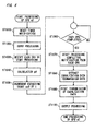
- FIG. 5 is a flowchart showing an operation of the active-side controller 10a.
- the timer 15a and the interruption control 14a of the active-side controller 10a are set in advance so as to notify the CPU a0 of interruption at intervals of a cycle T.
- the CPU a0 of the active-side controller 10a starts processing.
- Step ST1010 the notification from the timer 15a indicating that the cycle T has elapsed is reset.
- This reset is performed for waiting for the next notification of the cycle T from the timer 15a.
- Step ST1020 data is input from the I/O board 2a.
- the CPU a0 requests the I/O bus controller 13a to read input data from the I/O board 2a.
- the I/O bus controller 13a In response to the reading request, the I/O bus controller 13a reads data from a plurality of I/O boards 2a via the I/O bus 3a, and stores the read data as the input data 11a1 into the memory 11a.
- Step ST1030 the CPU a0 notifies the other CPUs to start processing. Predetermined values are written into the respective interruption notification registers for the CPUs a1 to an in the interruption control 14a.
- the interruption control 14a turns on the interruption signals 17a1 to 17an, to give notification that interruption occurs to the CPUs a1 to an.
- Step ST1040 the CPU a0 performs calculation of the calculation routine p0.
- the calculation routine p0 includes processing (calculation 1) of converting data to be used in calculation by the CPU a0 into a format suitable for the calculation, processing (calculation 2) of actually performing the calculation, and processing (calculation 3) of converting the calculation result into a data format suitable for output from the I/O board 2a.
- processing (calculation 3) of converting the calculation result by the calculation 2 into a format suitable for the I/O board 2a is performed, and the converted data is stored in the output data 11a2.
- Step ST1050 the value of the execution count pc0 in the memory 11a, which indicates the number of times the calculation routine p0 has been executed, is incremented by one.
- Step ST1060 completion of all the processes by the CPUs a1 to an described later is waited for.
- Step ST1070 after all the processes by the CPUs a1 to an have been completed, processing completion notification from each CPU is reset, and thus processing completion notification in the next cycle is waited for.
- Step ST1080 the resultant data of the calculation 1 and the resultant data of the calculation 2 (hereinafter, referred to as "p0 calculation data") in the calculation data pd0 to pdn are joined with each other, and the transmission data shown in FIG. 4 is stored into the equalization data transmission buffer 11a3.
- Step ST1090 the CPU a0 instructs the equalization bus controller 12a to transmit the transmission data in the equalization data transmission buffer 11a3 to the standby-side controller 10b.
- the equalization bus controller 12a transmits the data in the equalization data transmission buffer 11a3 to the standby-side controller 10b.
- the CPU a0 issues an instruction to perform processing of Step ST1100 without waiting for completion of the transmission by the equalization bus controller 12a in Step ST1090.
- Step ST1100 processing of outputting data to the I/O board 2a is performed.
- the CPU a0 requests the I/O bus controller 13a to perform writing from the output data 11a2 of the memory 11a into the I/O board 2a.
- the I/O bus controller 13a In response to the writing request, the I/O bus controller 13a writes the data into the I/O board 2a via the I/O bus 3a.
- FIG. 6 is a flowchart showing an operation of the CPU a1 (to CPU an) of the active-side controller 10a.
- Step ST1110 the processing start notification from the CPU a0 is reset.
- This reset is performed for waiting for the next notification.
- Step ST1120 calculation of the calculation routine p1 by the CPU a1 is performed.
- the calculation routine p1 includes processing (calculation 1) of converting data to be used in calculation by the CPU a1 into a format suitable for the calculation, processing (calculation 2) of actually performing the calculation, and processing (calculation 3) of converting the calculation result into a data format suitable for output from the I/O board 2a.
- processing (calculation 3) of converting the calculation result by the calculation 2 into a format suitable for the I/O board 2a is performed, and the converted data is stored in the output data 11a2.
- Step ST1030 the value of the execution count pc1 in the memory 11a, which indicates the number of times the calculation routine p1 has been executed, is incremented by one.
- Step ST1140 the CPU a0 is notified of processing completion.
- the notification of processing completion may be given via the interruption control 14a or may be given via the memory 11a.
- a timer 15b and an interruption control 14b of the standby-side controller 10b are set in advance so as to notify a CPU b0 of interruption at intervals of the cycle T, as in the active-side controller 10a.
- the active-side controller 10a and the standby-side controller 10b are not configured to synchronize their timings, but operate asynchronously.
- FIG. 7 is a flowchart showing an operation of the CPU b0 of the standby-side controller 10b.
- Processing in steps ST2010 to ST2030 is the same as processing in steps ST1010 to ST1030 in FIG. 5 performed by the CPU a0 of the active-side controller 10a.
- the CPU b0 acquires data from the I/O board 2b, stores the data as the input data 11b1 in the memory 11b, performs data processing by itself, and then instructs the other CPUs to perform similar processing.
- Step ST2035 the CPU b0 confirms a content of an equalization data reception buffer that is different from a buffer by which the equalization bus controller 12b receives equalization data at present, and acquires the data size from a part where a CPU identification number of data is 0.
- calculation data corresponding to the size is acquired and then expanded in the calculation data pd0 in the memory 11b.
- Processing in steps ST2040 to ST2070 and ST2100 is the same as processing in steps ST1040 to ST1070 and ST1100 performed by the CPU a0 of the active-side controller 10a in FIG. 5 .
- connection to a control target device is cut in the I/O board 2b, and therefore output data is not transmitted to the device.
- FIG. 8 is a flowchart showing an operation of a CPU b1 (to CPU bn) of the standby-side controller.
- Processing in steps ST2110 and ST2120 to ST2140 is the same as processing in steps ST1110 and ST1120 to ST1140 in FIG. 6 performed by the CPU a1 of the active-side controller 10a.
- Step ST2115 is added after Step ST2110.
- Step ST2115 as in Step ST2035 in FIG. 7 , the CPU b1 confirms a content of an equalization data reception buffer that is different from a buffer by which the equalization bus controller 12b receives equalization data at present, and acquires the data size from a part where a CPU identification number of data is 1.
- the calculation data corresponding to the size is acquired and then expanded in the calculation data pd1 in the memory 11b.
- FIG. 9 and FIG. 10 are timing charts showing the summary of the operation of the system 100 described thus far.
- An arrow in each chart indicates transmission of a signal or data.
- Arrows A1 and A2 in FIG. 9 are linked with arrows A1 and A2 in FIG. 10 .
- timings of the active-side controller 10a and the standby-side controller 10b can be visually understood.
- the standby dual redundant system 100 makes it unnecessary to provide a bus controller for each CPU in equalization processing for data to be processed by a plurality of CPUs.
- equalization data bus 20 and the I/O buses 3a and 3b are configured as independent buses, and their respective I/O bus controllers are also independent from each other, it becomes possible to perform transmission/reception of equalization data and transmission/reception with each I/O board simultaneously, thus realizing high-speed processing.
- Embodiment 2 of the present invention will be described focusing on a difference from Embodiment 1 with reference to the drawings.
- the interruption controls 14a and 14b are used for notifying each CPU to start processing.
- a flag is provided for a timer, and ON/OFF of the flag is used as an interruption notification signal.
- FIG. 11 is a flowchart showing an operation of the CPU a0 of the active-side controller according to the present embodiment.
- FIG. 5 showing an operation of the CPU a0 of Embodiment 1
- FIG. 11 showing an operation of the CPU a0 of the present Embodiment is that, first, in FIG. 5 , processing starts after interruption to start the processing occurs.
- Step ST1005 when the CPU a0 confirms that the flag indicating start of processing is turned on, the flag is reset in Step ST1010, and then data input processing from the I/O board is performed in Step ST1020.
- Step ST1030 each flag for instructing the other CPUs to start processing, which is provided in the timer or in a memory area, is turned on.
- FIG. 12 is a flowchart showing an operation of the CPU a1 (to an) of the active-side controller according to the present embodiment.
- FIG. 6 showing an operation of the CPU a1 of Embodiment 1
- FIG. 12 showing an operation of the CPU a1 of the present Embodiment is that, first, in FIG. 6 , processing starts after interruption to start processing occurs.
- Step ST1105 when the CPU a1 confirms that the flag indicating start of processing is turned on, the flag is reset in Step ST1110, and then the calculation p1 is performed in Step ST1120.
- the standby dual redundant system according to Embodiment 2 of the present invention uses ON/OFF of a flag provided in the system as substitute for an interruption notification signal, thereby providing a simple standby dual redundant system that does not need special interruption control.
- Embodiment 3 of the present invention will be described focusing on a difference from Embodiment 2 with reference to the drawings.
- FIG. 13 is a diagram showing the configuration of data stored in a memory 311a of the active-side controller according to the present embodiment.
- a plurality of calculation routines are allocated to each CPU.
- a numeric character following "p" indicates a number of each CPU that executes the corresponding calculation routine
- a numeric character following a hyphen indicates a serial number of each calculation routine allocated to the CPU having the above number.
- FIG. 14 and FIG. 15 are timing charts showing the operation states of the respective controllers of the standby dual redundant system according to the present embodiment.
- An arrow in each chart indicates transmission of a signal or data.
- Arrows A1 and A2 in FIG. 14 are linked with arrows A1 and A2 in FIG. 15 .
- a plurality of calculations of calculation routines p0-1 to p0-x can be performed by the CPU a0 of the active-side controller, and similarly, a plurality of calculations of calculation routines p1-1 to pn-z can be performed by the CPUs a1 to an.
- the memory 311a is configured to have attribute data indicating a number of each CPU that executes a calculation routine, whereby each CPU can be assigned in advance with calculation routines to perform calculations in a multi-CPU environment.
- Embodiment 4 of the present invention will be described focusing on a difference from Embodiment 3 with reference to the drawings.
- FIG. 16 is a diagram showing a part of the configuration of data stored in a memory 411a of the active-side controller.
- setting items of an execution CPU number, an execution cycle setting, an execution offset setting, an execution count, and a transmission count are provided as attribute data.
- an execution offset can be set for the calculation routine that is executed in a cycle of a multiple of the cycle T.
- a timing to execute the calculation routine is set by a decimal number with the cycle T defined as 1.
- the calculation routine is executed in a quadruple cycle of the cycle T and with a lag of 1/4 of the cycle T from the timer.
- a calculation routine that operates in a cycle of a multiple of the cycle T exists as described above. That is, the calculation routines include the ones that operate in different cycles.
- equalization data is transmitted in the cycle T. Therefore, it is not necessary to transmit data of a calculation routine that does not operate on a cycle T basis.
- the execution count and the transmission count are added in the memory 411a and are used.
- equalization transmission data is generated by the CPU a0 of the active-side controller, the transmission count is compared with the execution count, and if the two count values are different from each other, calculation data of the corresponding calculation routine is determined to be transmitted as equalization data, and is transmitted to the transmission buffer.
- transmission count is rewritten to the value of the execution count, after transmission processing to the transmission buffer is completed.
- the standby dual redundant system provides the execution cycle setting and the execution offset setting in the memory 411a, thereby executing calculation in a cycle of a multiple of the cycle T, and further, as necessary, with an execution offset set for each calculation routine.
- Embodiment 5 of the present invention will be described focusing on a difference from Embodiment 4 with reference to the drawings.
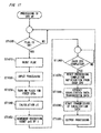
- FIG. 17 is a diagram showing a part of the configuration of data stored in a memory 511a of the active-side controller.
- An execution continuation allowance setting is added for the calculation routine to be executed by each CPU.
- a mechanism is added in which, in the case where the execution continuation allowance setting is set at "allowed", even if the calculation has not been completed within the set cycle T, the calculation processing is temporarily held, to perform input and output of data, and then the calculation processing is restarted and continued at the next cycle.
- the standby dual redundant system according to the present Embodiment can provide a standby dual redundant system that does not affect the processing as a whole even if some of the processing routines have greatly different processing times.
- Embodiment 6 of the present invention will be described focusing on a difference from Embodiment 1 with reference to the drawings.
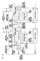
- FIG. 18 is a diagram showing the configuration of a standby dual redundant system 600 (hereinafter, referred to as a system 600).
- a CPU board 601a of an active-side controller 610a two equalization bus controllers 12a1 and 12b2 are provided.
- the equalization bus controller 12a1 and the equalization bus controller 12b1 are connected via the equalization data bus 20, and the equalization bus controller 12a2 and the equalization bus controller 12b2 are connected via an equalization data bus 21.
- FIG. 19 is a diagram showing a part of the configuration of equalization transmission data transmitted from the active-side controller 610a to the standby-side controller 610b.
- the execution counts pc0 to pcn for respective calculation routines are provided as serial numbers.
- the CPU a0 of the active-side controller transmits the transmission data shown in FIG. 19 to the two controllers of the equalization bus controller 12a1 and the equalization bus controller 12a2.
- each CPU of the standby-side controller compares the execution count of the equalization reception data received by the equalization bus controller 12b2 via the equalization bus controller 12a1 with the execution count of the equalization reception data received by the equalization bus controller 12b2 via the equalization bus controller 12a2, and expands one of these calculation data that has the larger count value in the memory 11b.
- the standby dual redundant system 600 has dual equalization bus controllers and dual equalization data buses and provides counts for data that is transmitted and received, whereby, even if a failure occurs on either route, data equalization can be performed by using the other route.
- Embodiment 7 of the present invention will be described focusing on a difference from Embodiment 1 with reference to the drawings.
- FIG. 20 is a diagram showing the configuration of a standby dual redundant system 700 (hereinafter, referred to as a system 700).
- FIG. 21 is a diagram showing the data configurations in memories 711a and 711b which are commonly used by the CPUs in this case.
- FIG. 22 is a diagram showing the configurations of the memories a0 to an and the memories b0 to bn individually added for the respective CPUs.
- the memory 711a or the memory 711b stores only data that are commonly used, so that the frequency of access to the memory 711a or the memory 711b can be suppressed.
- Embodiment 8 of the present invention will be described focusing on a difference from Embodiment 1 with reference to the drawings.
- FIG. 23 is a diagram showing the configuration of equalization transmission data of Embodiment 8.
- each CPU of the standby-side controller compares the identification code and the version code of each calculation routine in the received equalization data with the identification code and the version code of each calculation routine that the standby-side controller has.
- the entire system can be prevented from being equalized with wrong data, thus improving the reliability of the standby dual redundant system.
Abstract
Description
- The present invention relates to a standby dual redundant system with dual controllers each having multiple CPUs to perform different calculations by the respective CPUs in a constant cycle.
- Conventionally, as an equalization controller for data in the case of using multiple CPUs, the CPUs have respective system bus controllers, and each CPU is connected to a system bus via the system bus controller. As an example of such configurations, a standby dual redundant system as shown in
Patent Document 1 is proposed. - In this system, equalization data is transmitted from an active-side CPU to a standby-side CPU by using the system bus controller, thereby realizing data equalization between the two controllers.
- Patent Document 1: Japanese Laid-Open Patent Publication
JP-A-2002-149 212
(paragraphs [0020] to [0022],FIG. 1 ,FIG. 3 ) - In a standby dual redundant system having multiple CPUs each performing a different calculation in a constant cycle, a bus is provided for transferring data to be equalized from an active-side CPU to a standby-side CPU. In the equalization controller shown in
Patent Document 1, since each CPU has the bus controller for equalizing data, if the number of the CPUs increases, the same number of bus controllers as the increased CPUs are required. - Thus, there is a problem that the circuit scale is enlarged.
- In addition, transmission/reception of equalization data and transmission/reception of data with an I/O board use the same system bus. Therefore, transmission/reception of equalization data and transmission/reception with the I/O board cannot be performed simultaneously, and thus there is a problem that response of data transfer cannot be improved.
- The present invention has been made to solve the above problems, and an object of the present invention is to provide a standby dual redundant system that can suppress the circuit scale without increasing the number of bus controllers even if the number of CPUs increases, and allows simultaneous execution of transmission/reception of equalization data between controllers and transmission/reception of data between an I/O board and a CPU.
- A standby dual redundant system according to the present invention includes two controllers such that, when one of the controllers operates as an active-side controller, the other controller operates as a standby-side controller, each controller having therein: a plurality of CPUs; a memory; an I/O board; an I/O bus controller for performing transmission and reception of data among the plurality of CPUs, the memory, and the I/O board; and an equalization bus controller for transmitting equalization data used for equalizing device states of the active-side controller and the standby-side controller, from the active-side controller to the standby-side controller via an equalization data bus, the equalization bus controller being independent from the I/O bus controller.
- In the standby dual redundant system according to the present invention, each controller has therein: a plurality of CPUs; a memory; an I/O board; an I/O bus controller for performing transmission and reception of data among the plurality of CPUs, the memory, and the I/O board; and an equalization bus controller for transmitting equalization data used for equalizing device states of the active-side controller and the standby-side controller, from the active-side controller to the standby-side controller via an equalization data bus, the equalization bus controller being independent from the I/O bus controller.
- Therefore, it becomes unnecessary to provide a bus controller for each CPU in equalization processing for data to be processed by a plurality of CPUs.
- In addition, since the equalization data bus and the I/O bus are configured as independent buses, and their respective bus controllers are also independent from each other, it becomes possible to perform transmission/reception of equalization data and transmission/reception with the I/O board simultaneously, thus realizing high-speed processing.
-
- FIG. 1
- is a diagram showing the configuration of a standby dual redundant system according to
Embodiment 1 of the present invention. - FIG. 2
- is a diagram showing the configuration of an interruption control in the standby dual redundant system according to
Embodiment 1 of the present invention. - FIG. 3
- is a diagram showing the configuration of a memory in the standby dual redundant system according to
Embodiment 1 of the present invention. - FIG. 4
- is a diagram showing the configuration of equalization data transmission data in the standby dual redundant system according to
Embodiment 1 of the present invention. - FIG. 5
- is a flowchart showing an operation of a CPU a0 of an active-side controller in the standby dual redundant system according to
Embodiment 1 of the present invention. - FIG. 6
- is a flowchart showing an operation of a CPU a1 of the active-side controller in the standby dual redundant system according to
Embodiment 1 of the present invention. - FIG. 7
- is a flowchart showing an operation of a CPU b0 of a standby-side controller in the standby dual redundant system according to
Embodiment 1 of the present invention. - FIG. 8
- is a flowchart showing an operation of a CPU b1 of the standby-side controller in the standby dual redundant system according to
Embodiment 1 of the present invention. - FIG. 9
- is a timing chart showing an operation of the standby dual redundant system according to
Embodiment 1 of the present invention. - FIG. 10
- is a timing chart showing an operation of the standby dual redundant system according to
Embodiment 1 of the present invention. - FIG. 11
- is a flowchart showing an operation of a CPU a0 of an active-side controller in a standby dual redundant system according to
Embodiment 2 of the present invention. - FIG. 12
- is a flowchart showing an operation of a CPU a1 of the active-side controller in the standby dual redundant system according to
Embodiment 2 of the present invention. - FIG. 13
- is a diagram showing the configuration of a memory in a standby dual redundant system according to Embodiment 3 of the present invention.
- FIG. 14
- is a timing chart showing an operation of the standby dual redundant system according to Embodiment 3 of the present invention.
- FIG. 15
- is a timing chart showing an operation of the standby dual redundant system according to Embodiment 3 of the present invention.
- FIG. 16
- is a diagram showing the configuration of a memory in a standby dual redundant system according to
Embodiment 4 of the present invention. - FIG. 17
- is a diagram showing the configuration of a memory in a standby dual redundant system according to Embodiment 5 of the present invention.
- FIG. 18
- is a diagram showing the configuration of a standby dual redundant system according to Embodiment 6 of the present invention.
- FIG. 19
- is a diagram showing the configuration of equalization transmission data in the standby dual redundant system according to Embodiment 6 of the present invention.
- FIG. 20
- is a diagram showing the configuration of a standby dual redundant system according to Embodiment 7 of the present invention.
- FIG. 21
- is a diagram showing the configurations of common memories in the standby dual redundant system according to Embodiment 7 of the present invention.
- FIG. 22
- is a diagram showing the configurations of individual memories in the standby dual redundant system according to Embodiment 7 of the present invention.
- FIG. 23
- is a diagram showing the configuration of equalization data transmission data in a standby dual redundant system according to Embodiment 8 of the present invention.
- Hereinafter,
Embodiment 1 of the present invention will be described with reference to the drawings. -
FIG. 1 is a diagram showing the configuration of a standby dual redundant system 100 (hereinafter, referred to as a system 100). - In
FIG. 1 , thesystem 100 includes an active-side controller 10a, a standby-side controller 10b, and anequalization data bus 20. - A calculation result of the active-
side controller 10a is sent to the standby-side controller 10b via theequalization data bus 20. - The standby-
side controller 10b has the same configuration as the active-side controller 10a. Therefore, the configuration of each controller will be described based on, mainly, the active-side controller 10a. - Here, the case where the two controllers are fixed as the active-
side controller 10a and the standby-side controller 10b will be described. However, in practice, since the active-side controller 10a and the standby-side controller 10b have the same configuration, their roles may be replaced with each other. - The active-
side controller 10a includes a CPU board 1a, a plurality of I/O boards 2a, and an I/O bus 3a. Input data needed for a calculation routine of the CPU board 1a is obtained by being read from the I/O board 2a via the I/O bus 3a. - In addition, output data that is a calculation result of the calculation routine of the CPU board 1a is written into the I/
O board 2a via the I/O bus 3a. - Output of data to a device controlled by the
system 100 is performed by the I/O board 2a in the active-side controller 10a. - Even if output data is written onto an I/
O board 2b side in the standby-side controller 10b, data output to the device is cut in the I/O board 2b, so that the output data is not transmitted from the standby-side controller 10b to the device. - The CPU board 1a includes a plurality of CPUs from a CPU a0 to a CPU an, a
memory 11a, anequalization bus controller 12a, an I/O bus controller 13a, aninterruption control 14a which corresponds to an execution control section in claims, and atimer 15 a. - The plurality of CPUs from the CPU a0 to the CPU an perform respective different calculations.
- In the
memory 11a, data used in calculation by each CPU is placed. - The I/
O bus controller 13a performs data transmission between thememory 11a and the plurality of I/O boards 2a via the I/O bus 3a in accordance with a reading request or a writing request for data to be used by each CPU. - The
equalization bus controller 12a of the active-side controller 10a transmits a result of calculation performed by each CPU of the active-side controller 10a, or the like, to anequalization bus controller 12b of the standby-side controller 10b via theequalization data bus 20. - The
equalization bus controller 12b of the standby-side controller 10b stores the received data into amemory 11b of the standby-side controller 10b. - In addition, the
interruption control 14a notifies each of the CPUs a0 to an of interruption, using aninterruption signal bus 16a. - Further, the
timer 15a is connected to theinterruption control 14a, whereby a predetermined CPU can be notified of interruption at regular intervals. -
FIG. 2 is a diagram showing the configuration of theinterruption control 14a. - The
interruption control 14a is provided with respective interruption notification registers for the CPUs a0 to an. For example, when data is set in the interruption notification register for CPU a0, an interruption signal 17a0 to the CPU a0 is turned on, whereby the CPU a0 is notified of interruption. - The interruption notification registers and the interruption signals 17a0 to 17an are provided for the respective CPUs.
- The interruption notification registers for the CPUs a0 to an are accessible from each other's CPU, and each CPU can notify another CPU of interruption.
-
FIG. 3 is a diagram showing the configuration of data stored in thememory 11a and thememory 11b. - The
memory 11a and thememory 11b have the same configuration. Therefore, thememory 11a will be described. - Input data 11a1 is data obtained by being read from the I/
O board 2a. - Output data 11a2 is data to be written into the I/
O board 2a. - The input data 11a1 and the output data 11a2 are stored in a format used in transmission and reception between the I/
O board 2a and a control target device. - In addition, in the
memory 11a, calculation routines p0 to pn are stored, which are performed by the CPUs a0 to an, respectively. - Actually, the calculation routines p0 to pn each include processing (calculation 1) of converting, from the input data 11a1, data to be used in calculation by each CPU into a format suitable for the calculation, processing (calculation 2) of actually performing the calculation, and processing (calculation 3) of converting the calculation result into a data format suitable for output from the I/
O board 2a. - In addition, in the
memory 11a, data for calculation used in the calculation routines p0 to pn performed by the CPUs a0 to an are arranged in the order from calculation data pd0 to calculation data pdn for the respective CPUs. - Specific contents of these calculation data will be described with reference to the calculation data pd0 used by the CPU a0.
- The calculation data pd0 is actually composed of a plurality of data.
- These data are classified into three types of data.
- The first type of data is data obtained by acquiring data to be used in the calculation routine p0 for CPU a0 from the input data 11a1 and then converting the data into a format suitable for the
calculation 2 by thecalculation 1 in the calculation routine p0. - The second type of data is composed of data obtained as a result of the
calculation 2 in the calculation routine p0 and an accumulated data group of such data in the past. - The third type of data is data obtained by converting the resultant data of the
calculation 2 in the calculation routine p0 into a format of output data to the I/O board 2a by the calculation 3 in the calculation routine p0. - Further, the
memory 11a has an equalization data transmission buffer 11a3, an equalization data reception buffer 11a4, and an equalization data reception buffer 11a5. - The equalization data transmission buffer 11a3 is used when the controller operates as the active-
side controller 10a. - The
equalization bus controller 12a of the active-side controller 10a transmits a content of the equalization data transmission buffer 11a3 to theequalization bus controller 12b of the standby-side controller 10b. - In addition, in the transmission, the
equalization bus controller 12a adds a checksum used for confirmation of the validity of the transmitted data. - The equalization data reception buffer 11a4 and the equalization data reception buffer 11a5 are used when the controller operates as the standby-side controller.
- This point will be described below, with reference to an operation of the standby-
side controller 10b. - The
equalization bus controller 12b of the standby-side controller 10b confirms data received from the active-side controller 10a, by using a checksum. - Then, if the received data is determined to be valid, the received data is stored alternately into an equalization data reception buffer 11b4 or an equalization data reception buffer 11b5. If the received data is determined to be invalid, the received data is discarded.
- At this time, the other reception buffer that is not used for the data reception by the
equalization bus controller 12b on the standby side is used for data processing by the CPU on the standby side. - Here, the description returns to the active-
side controller 10a. - In the
memory 11a of the active-side controller 10a, the numbers of times the calculation routines p0 to pn are respectively executed by the CPUs a0 to an, are stored as execution counts pc0 to pcn. - Even in the case of overflow, these count values do not become abnormal but are counted again from 0.
-
FIG. 4 is a diagram showing the configuration of transmission data stored in the equalization data transmission buffer 11a3. - Three types of data, i.e., an identification number of each CPU, a calculation data size needed for storing a result of the calculation routine for each CPU, and the calculation data, are stored as one set, and the respective sets of data of the calculation routine p0 for the CPU a0 to the calculation routine pn for the CPU an are joined with each other.
- Next, an operation of the active-
side controller 10a will be described. -
FIG. 5 is a flowchart showing an operation of the active-side controller 10a. - The
timer 15a and theinterruption control 14a of the active-side controller 10a are set in advance so as to notify the CPU a0 of interruption at intervals of a cycle T. - First, based on the interruption notification, the CPU a0 of the active-
side controller 10a starts processing. - First, in Step ST1010, the notification from the
timer 15a indicating that the cycle T has elapsed is reset. - This reset is performed for waiting for the next notification of the cycle T from the
timer 15a. - Next, in Step ST1020, data is input from the I/
O board 2a. - The CPU a0 requests the I/
O bus controller 13a to read input data from the I/O board 2a. - In response to the reading request, the I/
O bus controller 13a reads data from a plurality of I/O boards 2a via the I/O bus 3a, and stores the read data as the input data 11a1 into thememory 11a. - Next, in Step ST1030, the CPU a0 notifies the other CPUs to start processing. Predetermined values are written into the respective interruption notification registers for the CPUs a1 to an in the
interruption control 14a. - Then, the
interruption control 14a turns on the interruption signals 17a1 to 17an, to give notification that interruption occurs to the CPUs a1 to an. - Next, in Step ST1040, the CPU a0 performs calculation of the calculation routine p0.
- As described above, the calculation routine p0 includes processing (calculation 1) of converting data to be used in calculation by the CPU a0 into a format suitable for the calculation, processing (calculation 2) of actually performing the calculation, and processing (calculation 3) of converting the calculation result into a data format suitable for output from the I/
O board 2a. - First, data in the input data 11a1, to be used in calculation by the CPU a0, is converted into a format suitable for calculation of the calculation routine p0, and then is stored as the calculation data pd0 (calculation 1).
- Next, the main processing by
calculation 2 is executed, and the calculation result is stored to be added to the calculation data pd0 (calculation 2). - Further, processing (calculation 3) of converting the calculation result by the
calculation 2 into a format suitable for the I/O board 2a is performed, and the converted data is stored in the output data 11a2. - Next, in Step ST1050, the value of the execution count pc0 in the
memory 11a, which indicates the number of times the calculation routine p0 has been executed, is incremented by one. - Next, in Step ST1060, completion of all the processes by the CPUs a1 to an described later is waited for.
- Next, in Step ST1070, after all the processes by the CPUs a1 to an have been completed, processing completion notification from each CPU is reset, and thus processing completion notification in the next cycle is waited for.
- Next, in Step ST1080, the resultant data of the
calculation 1 and the resultant data of the calculation 2 (hereinafter, referred to as "p0 calculation data") in the calculation data pd0 to pdn are joined with each other, and the transmission data shown inFIG. 4 is stored into the equalization data transmission buffer 11a3. - Next, in Step ST1090, the CPU a0 instructs the
equalization bus controller 12a to transmit the transmission data in the equalization data transmission buffer 11a3 to the standby-side controller 10b. - In response to the instruction from the CPU a0, the
equalization bus controller 12a transmits the data in the equalization data transmission buffer 11a3 to the standby-side controller 10b. - Next, the CPU a0 issues an instruction to perform processing of Step ST1100 without waiting for completion of the transmission by the
equalization bus controller 12a in Step ST1090. - In Step ST1100, processing of outputting data to the I/
O board 2a is performed. - The CPU a0 requests the I/
O bus controller 13a to perform writing from the output data 11a2 of thememory 11a into the I/O board 2a. - In response to the writing request, the I/
O bus controller 13a writes the data into the I/O board 2a via the I/O bus 3a. -
FIG. 6 is a flowchart showing an operation of the CPU a1 (to CPU an) of the active-side controller 10a. - Next, operations of the CPUs a1 to an other than the CPU a0 will be described with reference to
FIG. 6 . - Since the operations of the CPUs a1 to an are the same, in
FIG. 6 , the operation of the CPU a1 will be described. - First, when the CPU a1 has started processing in response to a processing start notification based on an instruction from the CPU a0, in Step ST1110, the processing start notification from the CPU a0 is reset.
- This reset is performed for waiting for the next notification.
- Next, in Step ST1120, calculation of the calculation routine p1 by the CPU a1 is performed. As described above, the calculation routine p1 includes processing (calculation 1) of converting data to be used in calculation by the CPU a1 into a format suitable for the calculation, processing (calculation 2) of actually performing the calculation, and processing (calculation 3) of converting the calculation result into a data format suitable for output from the I/
O board 2a. - First, input data in the input data 11a1, to be used in calculation by the CPU a1, is converted into a format suitable for calculation in the calculation routine p1, and then is stored as the calculation data pd1 (calculation 1).
- Next, the main processing by
calculation 2 is executed, and the calculation result is stored to be added to the calculation data pd1. - Further, processing (calculation 3) of converting the calculation result by the
calculation 2 into a format suitable for the I/O board 2a is performed, and the converted data is stored in the output data 11a2. - Next, in Step ST1030, the value of the execution count pc1 in the
memory 11a, which indicates the number of times the calculation routine p1 has been executed, is incremented by one. - Next, in Step ST1140, the CPU a0 is notified of processing completion.
- The notification of processing completion may be given via the
interruption control 14a or may be given via thememory 11a. - Next, an operation of the standby-
side controller 10b will be described. Also atimer 15b and aninterruption control 14b of the standby-side controller 10b are set in advance so as to notify a CPU b0 of interruption at intervals of the cycle T, as in the active-side controller 10a. - It is noted that the active-
side controller 10a and the standby-side controller 10b are not configured to synchronize their timings, but operate asynchronously. -
FIG. 7 is a flowchart showing an operation of the CPU b0 of the standby-side controller 10b. - Processing performed by the CPU b0 of the standby-
side controller 10b based on interruption notification from theinterruption control 14b will be described with reference toFIG. 7 . - Processing in steps ST2010 to ST2030 is the same as processing in steps ST1010 to ST1030 in
FIG. 5 performed by the CPU a0 of the active-side controller 10a. - Therefore, as in the case of the CPU a0 of the active-
side controller 10a, the CPU b0 acquires data from the I/O board 2b, stores the data as the input data 11b1 in thememory 11b, performs data processing by itself, and then instructs the other CPUs to perform similar processing. - In Step ST2035, the CPU b0 confirms a content of an equalization data reception buffer that is different from a buffer by which the
equalization bus controller 12b receives equalization data at present, and acquires the data size from a part where a CPU identification number of data is 0. - Next, the calculation data corresponding to the size is acquired and then expanded in the calculation data pd0 in the
memory 11b. - At this time, a common part with the equalization data (a part corresponding to the resultant data of the
calculation 1 and the resultant data of thecalculation 2 described above) is to be overwritten with the equalization data. - It is noted that the data corresponding to the result of the
calculation 2 is to be further overwritten by calculation in subsequent Step ST2040. - Processing in steps ST2040 to ST2070 and ST2100 is the same as processing in steps ST1040 to ST1070 and ST1100 performed by the CPU a0 of the active-
side controller 10a inFIG. 5 . - Regarding the I/
O board 2b of the standby-side controller 10b, during a period in which this controller is operating as a standby-side controller, connection to a control target device is cut in the I/O board 2b, and therefore output data is not transmitted to the device. -
FIG. 8 is a flowchart showing an operation of a CPU b1 (to CPU bn) of the standby-side controller. - Next, operations of the CPUs b1 to bn other than the CPU b0 will be described with reference to
FIG. 8 . - Since the operations of the CPUs b1 to bn are the same, in
FIG. 8 , the operation of the CPU b1 will be described. - Processing in steps ST2110 and ST2120 to ST2140 is the same as processing in steps ST1110 and ST1120 to ST1140 in
FIG. 6 performed by the CPU a1 of the active-side controller 10a. - A difference from
FIG. 6 is that processing of Step ST2115 is added after Step ST2110. - In Step ST2115, as in Step ST2035 in
FIG. 7 , the CPU b1 confirms a content of an equalization data reception buffer that is different from a buffer by which theequalization bus controller 12b receives equalization data at present, and acquires the data size from a part where a CPU identification number of data is 1. - Then, the calculation data corresponding to the size is acquired and then expanded in the calculation data pd1 in the
memory 11b. - At this time, a common part with the equalization data (a part corresponding to the resultant data of the
calculation 1 and the resultant data of thecalculation 2 described above) is to be overwritten with the equalization data. - It is noted that the data corresponding to the result of the
calculation 2 is to be further overwritten by calculation in subsequent Step ST2120. -
FIG. 9 andFIG. 10 are timing charts showing the summary of the operation of thesystem 100 described thus far. - An arrow in each chart indicates transmission of a signal or data.
- Arrows A1 and A2 in
FIG. 9 are linked with arrows A1 and A2 inFIG. 10 . - Comparing two charts side by side, timings of the active-
side controller 10a and the standby-side controller 10b can be visually understood. - The standby dual
redundant system 100 according toEmbodiment 1 of the present invention makes it unnecessary to provide a bus controller for each CPU in equalization processing for data to be processed by a plurality of CPUs. - In addition, since the
equalization data bus 20 and the I/O buses - Hereinafter,
Embodiment 2 of the present invention will be described focusing on a difference fromEmbodiment 1 with reference to the drawings. - In
Embodiment 1, the interruption controls 14a and 14b are used for notifying each CPU to start processing. - In the present embodiment, instead of using interruption, a flag is provided for a timer, and ON/OFF of the flag is used as an interruption notification signal.
-
FIG. 11 is a flowchart showing an operation of the CPU a0 of the active-side controller according to the present embodiment. - The difference between
FIG. 5 showing an operation of the CPU a0 ofEmbodiment 1 andFIG. 11 showing an operation of the CPU a0 of the present Embodiment is that, first, inFIG. 5 , processing starts after interruption to start the processing occurs. - Secondly, in
FIG. 11 , the processing start flag is monitored by a loop of Step ST1005. - In the present embodiment, since the CPU a0 monitors the flag, independent interruption control is not needed.
- In Step ST1005, when the CPU a0 confirms that the flag indicating start of processing is turned on, the flag is reset in Step ST1010, and then data input processing from the I/O board is performed in Step ST1020.
- Next, in Step ST1030, each flag for instructing the other CPUs to start processing, which is provided in the timer or in a memory area, is turned on.
- The other processing is the same as in
Embodiment 1. -
FIG. 12 is a flowchart showing an operation of the CPU a1 (to an) of the active-side controller according to the present embodiment. - The difference between
FIG. 6 showing an operation of the CPU a1 ofEmbodiment 1 andFIG. 12 showing an operation of the CPU a1 of the present Embodiment is that, first, inFIG. 6 , processing starts after interruption to start processing occurs. - Secondly, in
FIG. 12 , the processing start flag is monitored by a loop of Step ST1105. - In the present embodiment, since the CPU a1 monitors the flag, independent interruption control is not needed.
- In Step ST1105, when the CPU a1 confirms that the flag indicating start of processing is turned on, the flag is reset in Step ST1110, and then the calculation p1 is performed in Step ST1120.
- The other processing is the same as in
Embodiment 1. - Although a flowchart for the standby-
side controller 10b is not specifically shown, processing can be realized using a flag in a similar manner. - The standby dual redundant system according to
Embodiment 2 of the present invention uses ON/OFF of a flag provided in the system as substitute for an interruption notification signal, thereby providing a simple standby dual redundant system that does not need special interruption control. - Hereinafter, Embodiment 3 of the present invention will be described focusing on a difference from
Embodiment 2 with reference to the drawings. -
FIG. 13 is a diagram showing the configuration of data stored in amemory 311a of the active-side controller according to the present embodiment. - In the present embodiment, more calculation data and more calculation routines than the number of CPUs are provided.
- A plurality of calculation routines are allocated to each CPU.
- In
FIG. 13 , a numeric character following "p" indicates a number of each CPU that executes the corresponding calculation routine, and a numeric character following a hyphen indicates a serial number of each calculation routine allocated to the CPU having the above number. -
FIG. 14 andFIG. 15 are timing charts showing the operation states of the respective controllers of the standby dual redundant system according to the present embodiment. - An arrow in each chart indicates transmission of a signal or data.
- Arrows A1 and A2 in
FIG. 14 are linked with arrows A1 and A2 inFIG. 15 . - Comparing two charts side by side, timings of the active-side controller and the standby-side controller can be visually understood.
- By the above configuration of the
memory 311a, as shown inFIG. 14 andFIG. 15 , a plurality of calculations of calculation routines p0-1 to p0-x can be performed by the CPU a0 of the active-side controller, and similarly, a plurality of calculations of calculation routines p1-1 to pn-z can be performed by the CPUs a1 to an. - In the standby dual redundant system according to the present embodiment, the
memory 311a is configured to have attribute data indicating a number of each CPU that executes a calculation routine, whereby each CPU can be assigned in advance with calculation routines to perform calculations in a multi-CPU environment. - Hereinafter,
Embodiment 4 of the present invention will be described focusing on a difference from Embodiment 3 with reference to the drawings. -
FIG. 16 is a diagram showing a part of the configuration of data stored in amemory 411a of the active-side controller. - For each calculation routine, setting items of an execution CPU number, an execution cycle setting, an execution offset setting, an execution count, and a transmission count are provided as attribute data.
- By using the execution cycle setting item, it becomes possible to realize a calculation routine that is executed in a cycle of a multiple of the cycle T.
- In addition, an execution offset can be set for the calculation routine that is executed in a cycle of a multiple of the cycle T.
- In the execution offset setting, a timing to execute the calculation routine is set by a decimal number with the cycle T defined as 1.
- For example, in the case where an execution offset is set at 0.25 for a calculation routine that is executed in a cycle of quadruple of the cycle T, the calculation routine is executed in a quadruple cycle of the cycle T and with a lag of 1/4 of the cycle T from the timer.
- In the present embodiment, a calculation routine that operates in a cycle of a multiple of the cycle T exists as described above. That is, the calculation routines include the ones that operate in different cycles.
- On the other hand, equalization data is transmitted in the cycle T. Therefore, it is not necessary to transmit data of a calculation routine that does not operate on a cycle T basis.
- Therefore, in order to avoid retransmission of data of such calculation routines, the execution count and the transmission count are added in the
memory 411a and are used. - When equalization transmission data is generated by the CPU a0 of the active-side controller, the transmission count is compared with the execution count, and if the two count values are different from each other, calculation data of the corresponding calculation routine is determined to be transmitted as equalization data, and is transmitted to the transmission buffer.
- As a result of the comparison between the transmission count and the execution count, if they coincide with each other, it is determined that the data has been already transmitted and the corresponding calculation routine has not been newly executed, and the data is not transmitted to the transmission buffer.
- It is noted that the transmission count is rewritten to the value of the execution count, after transmission processing to the transmission buffer is completed.
- The standby dual redundant system according to the present Embodiment provides the execution cycle setting and the execution offset setting in the
memory 411a, thereby executing calculation in a cycle of a multiple of the cycle T, and further, as necessary, with an execution offset set for each calculation routine. - In addition, by providing the transmission count and comparing the transmission count with the execution count, unnecessary transmission of equalization data is reduced, whereby time taken to transmit and receive equalization data can be shortened.
- Hereinafter, Embodiment 5 of the present invention will be described focusing on a difference from
Embodiment 4 with reference to the drawings. -
FIG. 17 is a diagram showing a part of the configuration of data stored in amemory 511a of the active-side controller. - An execution continuation allowance setting is added for the calculation routine to be executed by each CPU.
- A mechanism is added in which, in the case where the execution continuation allowance setting is set at "allowed", even if the calculation has not been completed within the set cycle T, the calculation processing is temporarily held, to perform input and output of data, and then the calculation processing is restarted and continued at the next cycle.
- As a result of the addition of the execution continuation allowance setting, input and output of data are performed in the middle of the calculation routine for which the calculation processing is held. However, as long as the input and output operation does not cause any problem, a calculation routine that operates within the constant cycle T and a calculation routine that does not operate within the constant cycle T can coexist.
- The standby dual redundant system according to the present Embodiment can provide a standby dual redundant system that does not affect the processing as a whole even if some of the processing routines have greatly different processing times.
- Hereinafter, Embodiment 6 of the present invention will be described focusing on a difference from
Embodiment 1 with reference to the drawings. -
FIG. 18 is a diagram showing the configuration of a standby dual redundant system 600 (hereinafter, referred to as a system 600). - In a
CPU board 601a of an active-side controller 610a, two equalization bus controllers 12a1 and 12b2 are provided. - In addition, in a
CPU board 601b of a standby-side controller 610b, two equalization bus controllers 12b1 and 12b2 are provided. - The equalization bus controller 12a1 and the equalization bus controller 12b1 are connected via the
equalization data bus 20, and the equalization bus controller 12a2 and the equalization bus controller 12b2 are connected via anequalization data bus 21. - By thus providing dual sets of equalization bus controllers and dual
equalization data buses system 600 is enhanced. - Next, a transmission and reception method for transmission data using the dual equalization data buses in the
system 600 will be described. -
FIG. 19 is a diagram showing a part of the configuration of equalization transmission data transmitted from the active-side controller 610a to the standby-side controller 610b. - In the transmission data, the execution counts pc0 to pcn for respective calculation routines are provided as serial numbers.
- For starting transmission of equalization data in Step ST1090 in
FIG. 5 , the CPU a0 of the active-side controller transmits the transmission data shown inFIG. 19 to the two controllers of the equalization bus controller 12a1 and the equalization bus controller 12a2. - At the expansion of the equalization reception data in Step ST2035 in
FIG. 7 or in Step ST2115 inFIG. 8 , each CPU of the standby-side controller compares the execution count of the equalization reception data received by the equalization bus controller 12b2 via the equalization bus controller 12a1 with the execution count of the equalization reception data received by the equalization bus controller 12b2 via the equalization bus controller 12a2, and expands one of these calculation data that has the larger count value in thememory 11b. - The standby dual
redundant system 600 according to Embodiment 6 of the present invention has dual equalization bus controllers and dual equalization data buses and provides counts for data that is transmitted and received, whereby, even if a failure occurs on either route, data equalization can be performed by using the other route. - Hereinafter, Embodiment 7 of the present invention will be described focusing on a difference from
Embodiment 1 with reference to the drawings. -
FIG. 20 is a diagram showing the configuration of a standby dual redundant system 700 (hereinafter, referred to as a system 700). - For the CPUs a0 to an on a
CPU board 701a, individual memories a0 to an are respectively provided. - Similarly, for the CPUs b0 to bn on a
CPU board 701b, individual memories b0 to bn are respectively provided. -
FIG. 21 is a diagram showing the data configurations inmemories - In the
memory 711a, data commonly used by the CPUs a0 to an are placed. - Similarly, in the
memory 711b, data commonly used by the CPUs b0 to bn are placed. -
FIG. 22 is a diagram showing the configurations of the memories a0 to an and the memories b0 to bn individually added for the respective CPUs. - Only data individually used by the CPUs a0 to an and the CPUs b0 to bn are placed therein.
- In the standby dual
redundant system 700 according to Embodiment 7 of the present invention, thememory 711a or thememory 711b stores only data that are commonly used, so that the frequency of access to thememory 711a or thememory 711b can be suppressed. - Thus, the frequency of stoppage of calculation due to concentration of access from other CPUs is decreased, whereby the calculation performance of the
system 700 can be improved. - Hereinafter, Embodiment 8 of the present invention will be described focusing on a difference from
Embodiment 1 with reference to the drawings. -
FIG. 23 is a diagram showing the configuration of equalization transmission data of Embodiment 8. - In the transmission data, an identification code and a version code of each calculation routine are added.
- At the expansion of equalization data in Step ST2035 in
FIG. 7 or in - Step ST2115 in
FIG. 8 , each CPU of the standby-side controller compares the identification code and the version code of each calculation routine in the received equalization data with the identification code and the version code of each calculation routine that the standby-side controller has. - In the case where these codes do not coincide with each other, expansion processing for data is not performed and a user of the controller is notified of abnormality.
- In the standby dual redundant system according to Embodiment 8 of the present invention, even if calculation routines of the active-side controller and the standby-side controller become different from each other, the entire system can be prevented from being equalized with wrong data, thus improving the reliability of the standby dual redundant system.
- It is noted that, within the scope of the present invention, the above embodiments may be freely combined with each other, or each of the above embodiments may be modified or abbreviated as appropriate.
Claims (11)
- A standby dual redundant system including two controllers, in which, when one of the controllers operates as an active-side controller, the other controller is adapted to operate as a standby-side controller, each controller comprising therein:a plurality of CPUs;a memory;an I/O board;an I/O bus controller for performing transmission and reception of data among the plurality of CPUs, the memory, and the I/O board; andan equalization bus controller for transmitting equalization data used for equalizing device states of the active-side controller and the standby-side controller, from the active-side controller to the standby-side controller via an equalization data bus, the equalization bus controller being independent from the I/O bus controller.
- The standby dual redundant system according to claim 1,
each controller further comprising:- a timer; and- an execution control section for notifying each CPU to start processing in a constant cycle in accordance with the timer, wherein
one of the CPUs of the active-side controller, that has been notified by the execution control section of the active-side controller, is adapted to acquire data used for calculation by each CPU of the active-side controller from the I/O board, to input the data to the memory via the I/O bus controller, and then to give an instruction to execute calculations allocated to the respective CPUs of the active-side controller, and
after all the calculations by the CPUs have been finished, the one CPU is adapted to collect all results of the calculations by the CPUs to form the equalization data to be transmitted to the standby-side controller. - The standby dual redundant system according to claim 2,
wherein the memory has therein,
input data for collectively storing data input from the I/O board,
a calculation routine for storing a calculation routine to be executed by each CPU,
calculation data for storing the input data that is used in each calculation routine, a calculation result obtained by execution of the calculation routine using the input data, and the previous calculation result,
output data for collectively storing data to be output to the I/O board, an equalization data transmission buffer for collectively storing the equalization data to be transmitted to the standby-side controller when each controller operates as the active-side controller, and
two equalization data reception buffers for alternately receiving the equalization data from the active-side controller when each controller operates as the standby-side controller. - The standby dual redundant system according to claim 3, wherein
the standby-side controller is adapted to operate asynchronously with the active-side controller and in the same constant cycle as the active-side controller,
one of the CPUs of the standby-side controller, that has been notified to start processing by the execution control section of the standby-side controller, is adapted to acquire data used for calculation by each CPU of the standby-side controller from the I/O board of the standby-side controller, to input the data to the memory of the standby-side controller via the I/O bus controller of the standby-side controller, and then to expand the equalization data received from the active-side controller in the memory of the standby-side controller, to overwrite the data acquired from the I/O board of the standby-side controller, and
the one CPU is adapted to give an instruction to execute calculations allocated to the respective CPUs of the standby-side controller. - The standby dual redundant system according to claim 4, wherein the memory has attribute data of each calculation routine, and the attribute data of each calculation routine has at least one of:CPU information for specifying a number of the CPU that executes each calculation routine;execution cycle information for executing each calculation routine in a cycle of a multiple of the cycle of the timer;offset information for executing each calculation routine with a predetermined offset provided with respect to the multiple of the cycle of the timer,execution times information indicating the number of times each calculation routine has been executed,transmission times information indicating the number of times the equalization data has been transmitted to the standby-side controller, andcontinuous processing allowance information indicating a next processing method in the case where each calculation routine has not been finished within the cycle of the timer.
- The standby dual redundant system according to claim 5, wherein the attribute data stored in the memory of the active-side controller has the execution times information and the transmission times information, and a data configuration of the equalization data is determined based on comparison between the execution times information and the transmission times information.
- The standby dual redundant system according to claim 5, wherein the equalization data has the transmission times information, and the standby-side controller is adapted to execute calculations allocated to the respective CPUs, using one of the equalization data in the two reception buffers, whose transmission times information indicates a larger number of times.
- The standby dual redundant system according to claim 5,
wherein the memory includes,
a CPU memory for storing data individually used by each CPU, and a common memory for storing data commonly used by the plurality of CPUs. - The standby dual redundant system according to claim 1, wherein
the equalization data has an identification code and a version code of each calculation routine, and
each CPU of the standby-side controller is adapted to confirm the identification code and the version code, to execute calculations allocated to the respective CPUs. - The standby dual redundant system according to claim 1,
wherein the equalization bus controller and the equalization data bus each have a dual configuration. - The standby dual redundant system according to any one of claims 2 to 10,
wherein the one CPU is adapted to notify each CPU to start calculations allocated to the respective CPUs, by interruption control or based on identification of a state of a flag provided in the memory.
Applications Claiming Priority (1)
| Application Number | Priority Date | Filing Date | Title |
|---|---|---|---|
| PCT/JP2012/062003 WO2013168258A1 (en) | 2012-05-10 | 2012-05-10 | Standby dual redundant system |
Publications (3)
| Publication Number | Publication Date |
|---|---|
| EP2849005A1 true EP2849005A1 (en) | 2015-03-18 |
| EP2849005A4 EP2849005A4 (en) | 2016-07-06 |
| EP2849005B1 EP2849005B1 (en) | 2019-08-07 |
Family
ID=49550342
Family Applications (1)
| Application Number | Title | Priority Date | Filing Date |
|---|---|---|---|
| EP12876411.5A Active EP2849005B1 (en) | 2012-05-10 | 2012-05-10 | Standby dual redundant system |
Country Status (3)
| Country | Link |
|---|---|
| EP (1) | EP2849005B1 (en) |
| JP (1) | JP5908068B2 (en) |
| WO (1) | WO2013168258A1 (en) |
Families Citing this family (3)
| Publication number | Priority date | Publication date | Assignee | Title |
|---|---|---|---|---|
| JP6354535B2 (en) * | 2014-11-17 | 2018-07-11 | 富士電機株式会社 | Redundant control system and control device thereof |
| JP7023726B2 (en) * | 2018-01-25 | 2022-02-22 | 株式会社日立ハイテクソリューションズ | Duplex control system |
| JP7047728B2 (en) * | 2018-11-29 | 2022-04-05 | オムロン株式会社 | Controller and controller control method |
Family Cites Families (17)
| Publication number | Priority date | Publication date | Assignee | Title |
|---|---|---|---|---|
| US4608631A (en) * | 1982-09-03 | 1986-08-26 | Sequoia Systems, Inc. | Modular computer system |
| JPH02156363A (en) * | 1988-12-08 | 1990-06-15 | Fuji Electric Co Ltd | State change detecting method for cache memory |
| JP3206006B2 (en) * | 1991-01-25 | 2001-09-04 | 株式会社日立製作所 | Duplex bus control method and device |
| JP3139884B2 (en) * | 1993-06-14 | 2001-03-05 | 株式会社東芝 | Multi-element processing system |
| JP3360385B2 (en) * | 1993-12-28 | 2002-12-24 | 株式会社日立製作所 | Plant control device |
| GB2290891B (en) * | 1994-06-29 | 1999-02-17 | Mitsubishi Electric Corp | Multiprocessor system |
| JPH0944203A (en) * | 1995-07-26 | 1997-02-14 | Hitachi Ltd | Redundancy control system |
| JP2000305919A (en) * | 1999-04-23 | 2000-11-02 | Hitachi Ltd | Multiprocessor system and its synchronizing method, and vibration test device |
| JP4154853B2 (en) | 2000-11-13 | 2008-09-24 | 富士電機機器制御株式会社 | A redundant programmable controller and an equalization method for equalizing control data. |
| US7093158B2 (en) * | 2002-03-11 | 2006-08-15 | Hewlett-Packard Development Company, L.P. | Data redundancy in a hot pluggable, large symmetric multi-processor system |
| JP4161276B2 (en) * | 2004-12-17 | 2008-10-08 | 日本電気株式会社 | Fault-tolerant computer device and synchronization method thereof |
| JP2006031727A (en) * | 2005-08-17 | 2006-02-02 | Hitachi Ltd | Fail-safe controller |
| GB2477237B (en) * | 2006-01-13 | 2011-09-07 | Emerson Process Management | A method for redundant controller synchronization for bump-less failover during normal and mismatch conditions |
| JP4791909B2 (en) * | 2006-08-21 | 2011-10-12 | 株式会社東芝 | Control device having high-speed input / output function and control method of control data thereof |
| JP2009187314A (en) * | 2008-02-06 | 2009-08-20 | Fuji Electric Systems Co Ltd | Duplex controller system, cpu module, and program thereof |
| JP5239525B2 (en) * | 2008-06-06 | 2013-07-17 | 横河電機株式会社 | Multiplexed input / output module |
| JP4981951B2 (en) * | 2010-06-02 | 2012-07-25 | 株式会社トライテック | Distributed computing system |
-
2012
- 2012-05-10 JP JP2014514305A patent/JP5908068B2/en active Active
- 2012-05-10 EP EP12876411.5A patent/EP2849005B1/en active Active
- 2012-05-10 WO PCT/JP2012/062003 patent/WO2013168258A1/en active Application Filing
Also Published As
| Publication number | Publication date |
|---|---|
| JPWO2013168258A1 (en) | 2015-12-24 |
| EP2849005B1 (en) | 2019-08-07 |
| JP5908068B2 (en) | 2016-04-26 |
| EP2849005A4 (en) | 2016-07-06 |
| WO2013168258A1 (en) | 2013-11-14 |
Similar Documents
| Publication | Publication Date | Title |
|---|---|---|
| US5574848A (en) | Can interface selecting one of two distinct fault recovery method after counting a predetermined number of recessive bits or good can frames | |
| JP4050196B2 (en) | Electronic control device having supervisory control circuit | |
| US7769935B2 (en) | Communication system with master and slave exchanging control data in predetermined communication period | |
| US20040243738A1 (en) | Method for asynchronous DMA command completion notification | |
| EP2312457B1 (en) | Data processing apparatus, data processing method and computer-readable medium | |
| US7143226B2 (en) | Method and apparatus for multiplexing commands in a symmetric multiprocessing system interchip link | |
| US8583845B2 (en) | Multi-processor system and controlling method thereof | |
| EP2849005B1 (en) | Standby dual redundant system | |
| EP2157723A2 (en) | Data retransmission method and system | |
| CN102436430B (en) | Memory device, host controller and memory system | |
| JP5082407B2 (en) | Access conflict generation system in access conflict test | |
| EP3312726A1 (en) | Cpu monitoring device | |
| JP2011182258A (en) | Can (controller area network) system, communication unit, and communication method | |
| EP1988469B1 (en) | Error control device | |
| JP4372110B2 (en) | Data transfer circuit, multiprocessor system using the same, and data transfer method | |
| JP6133614B2 (en) | Fault log collection device, fault log collection method, and fault log collection program | |
| EP3428799B1 (en) | Data access device and access error notification method | |
| JP2006178786A (en) | Multi-node system, node device, inter-node cross-bus switch and failure processing method | |
| JP2008234014A (en) | Duplex controller system and operation-system/standby-system controller therefor | |
| JP5494039B2 (en) | Memory diagnostic method and control device for power conversion device | |
| JP2010086132A (en) | Hardware module control system | |
| JP6906369B2 (en) | Computer systems, their control methods, and programs | |
| US20150067703A1 (en) | Time series data processing device, time series data processing method and time series data processing program storage medium | |
| CN114928511A (en) | Data processing apparatus and data processing system | |
| KR101476585B1 (en) | Method and Apparatus for Serial Bus Protocol for Data Voting among the Redundant Controllers |
Legal Events
| Date | Code | Title | Description |
|---|---|---|---|
| PUAI | Public reference made under article 153(3) epc to a published international application that has entered the european phase |
Free format text: ORIGINAL CODE: 0009012 |
|
| 17P | Request for examination filed |
Effective date: 20141205 |
|
| AK | Designated contracting states |
Kind code of ref document: A1 Designated state(s): AL AT BE BG CH CY CZ DE DK EE ES FI FR GB GR HR HU IE IS IT LI LT LU LV MC MK MT NL NO PL PT RO RS SE SI SK SM TR |
|
| AX | Request for extension of the european patent |
Extension state: BA ME |
|
| DAX | Request for extension of the european patent (deleted) | ||
| RA4 | Supplementary search report drawn up and despatched (corrected) |
Effective date: 20160608 |
|
| RIC1 | Information provided on ipc code assigned before grant |
Ipc: G06F 11/20 20060101ALI20160602BHEP Ipc: G05B 9/03 20060101AFI20160602BHEP Ipc: G06F 11/07 20060101ALI20160602BHEP |
|
| GRAP | Despatch of communication of intention to grant a patent |
Free format text: ORIGINAL CODE: EPIDOSNIGR1 |
|
| STAA | Information on the status of an ep patent application or granted ep patent |
Free format text: STATUS: GRANT OF PATENT IS INTENDED |
|
| INTG | Intention to grant announced |
Effective date: 20190220 |
|
| GRAS | Grant fee paid |
Free format text: ORIGINAL CODE: EPIDOSNIGR3 |
|
| GRAA | (expected) grant |
Free format text: ORIGINAL CODE: 0009210 |
|
| STAA | Information on the status of an ep patent application or granted ep patent |
Free format text: STATUS: THE PATENT HAS BEEN GRANTED |
|
| AK | Designated contracting states |
Kind code of ref document: B1 Designated state(s): AL AT BE BG CH CY CZ DE DK EE ES FI FR GB GR HR HU IE IS IT LI LT LU LV MC MK MT NL NO PL PT RO RS SE SI SK SM TR |
|
| REG | Reference to a national code |
Ref country code: GB Ref legal event code: FG4D |
|
| REG | Reference to a national code |
Ref country code: CH Ref legal event code: EP Ref country code: AT Ref legal event code: REF Ref document number: 1164785 Country of ref document: AT Kind code of ref document: T Effective date: 20190815 |
|
| REG | Reference to a national code |
Ref country code: DE Ref legal event code: R096 Ref document number: 602012062830 Country of ref document: DE |
|
| REG | Reference to a national code |
Ref country code: IE Ref legal event code: FG4D |
|
| REG | Reference to a national code |
Ref country code: NL Ref legal event code: MP Effective date: 20190807 |
|
| REG | Reference to a national code |
Ref country code: LT Ref legal event code: MG4D |
|
| PG25 | Lapsed in a contracting state [announced via postgrant information from national office to epo] |
Ref country code: NO Free format text: LAPSE BECAUSE OF FAILURE TO SUBMIT A TRANSLATION OF THE DESCRIPTION OR TO PAY THE FEE WITHIN THE PRESCRIBED TIME-LIMIT Effective date: 20191107 Ref country code: PT Free format text: LAPSE BECAUSE OF FAILURE TO SUBMIT A TRANSLATION OF THE DESCRIPTION OR TO PAY THE FEE WITHIN THE PRESCRIBED TIME-LIMIT Effective date: 20191209 Ref country code: BG Free format text: LAPSE BECAUSE OF FAILURE TO SUBMIT A TRANSLATION OF THE DESCRIPTION OR TO PAY THE FEE WITHIN THE PRESCRIBED TIME-LIMIT Effective date: 20191107 Ref country code: SE Free format text: LAPSE BECAUSE OF FAILURE TO SUBMIT A TRANSLATION OF THE DESCRIPTION OR TO PAY THE FEE WITHIN THE PRESCRIBED TIME-LIMIT Effective date: 20190807 Ref country code: HR Free format text: LAPSE BECAUSE OF FAILURE TO SUBMIT A TRANSLATION OF THE DESCRIPTION OR TO PAY THE FEE WITHIN THE PRESCRIBED TIME-LIMIT Effective date: 20190807 Ref country code: NL Free format text: LAPSE BECAUSE OF FAILURE TO SUBMIT A TRANSLATION OF THE DESCRIPTION OR TO PAY THE FEE WITHIN THE PRESCRIBED TIME-LIMIT Effective date: 20190807 Ref country code: LT Free format text: LAPSE BECAUSE OF FAILURE TO SUBMIT A TRANSLATION OF THE DESCRIPTION OR TO PAY THE FEE WITHIN THE PRESCRIBED TIME-LIMIT Effective date: 20190807 |
|
| REG | Reference to a national code |
Ref country code: AT Ref legal event code: MK05 Ref document number: 1164785 Country of ref document: AT Kind code of ref document: T Effective date: 20190807 |
|
| PG25 | Lapsed in a contracting state [announced via postgrant information from national office to epo] |
Ref country code: AL Free format text: LAPSE BECAUSE OF FAILURE TO SUBMIT A TRANSLATION OF THE DESCRIPTION OR TO PAY THE FEE WITHIN THE PRESCRIBED TIME-LIMIT Effective date: 20190807 Ref country code: ES Free format text: LAPSE BECAUSE OF FAILURE TO SUBMIT A TRANSLATION OF THE DESCRIPTION OR TO PAY THE FEE WITHIN THE PRESCRIBED TIME-LIMIT Effective date: 20190807 Ref country code: GR Free format text: LAPSE BECAUSE OF FAILURE TO SUBMIT A TRANSLATION OF THE DESCRIPTION OR TO PAY THE FEE WITHIN THE PRESCRIBED TIME-LIMIT Effective date: 20191108 Ref country code: IS Free format text: LAPSE BECAUSE OF FAILURE TO SUBMIT A TRANSLATION OF THE DESCRIPTION OR TO PAY THE FEE WITHIN THE PRESCRIBED TIME-LIMIT Effective date: 20191207 Ref country code: RS Free format text: LAPSE BECAUSE OF FAILURE TO SUBMIT A TRANSLATION OF THE DESCRIPTION OR TO PAY THE FEE WITHIN THE PRESCRIBED TIME-LIMIT Effective date: 20190807 Ref country code: LV Free format text: LAPSE BECAUSE OF FAILURE TO SUBMIT A TRANSLATION OF THE DESCRIPTION OR TO PAY THE FEE WITHIN THE PRESCRIBED TIME-LIMIT Effective date: 20190807 |
|
| PG25 | Lapsed in a contracting state [announced via postgrant information from national office to epo] |
Ref country code: TR Free format text: LAPSE BECAUSE OF FAILURE TO SUBMIT A TRANSLATION OF THE DESCRIPTION OR TO PAY THE FEE WITHIN THE PRESCRIBED TIME-LIMIT Effective date: 20190807 |
|
| PG25 | Lapsed in a contracting state [announced via postgrant information from national office to epo] |
Ref country code: IT Free format text: LAPSE BECAUSE OF FAILURE TO SUBMIT A TRANSLATION OF THE DESCRIPTION OR TO PAY THE FEE WITHIN THE PRESCRIBED TIME-LIMIT Effective date: 20190807 Ref country code: RO Free format text: LAPSE BECAUSE OF FAILURE TO SUBMIT A TRANSLATION OF THE DESCRIPTION OR TO PAY THE FEE WITHIN THE PRESCRIBED TIME-LIMIT Effective date: 20190807 Ref country code: AT Free format text: LAPSE BECAUSE OF FAILURE TO SUBMIT A TRANSLATION OF THE DESCRIPTION OR TO PAY THE FEE WITHIN THE PRESCRIBED TIME-LIMIT Effective date: 20190807 Ref country code: EE Free format text: LAPSE BECAUSE OF FAILURE TO SUBMIT A TRANSLATION OF THE DESCRIPTION OR TO PAY THE FEE WITHIN THE PRESCRIBED TIME-LIMIT Effective date: 20190807 Ref country code: PL Free format text: LAPSE BECAUSE OF FAILURE TO SUBMIT A TRANSLATION OF THE DESCRIPTION OR TO PAY THE FEE WITHIN THE PRESCRIBED TIME-LIMIT Effective date: 20190807 Ref country code: DK Free format text: LAPSE BECAUSE OF FAILURE TO SUBMIT A TRANSLATION OF THE DESCRIPTION OR TO PAY THE FEE WITHIN THE PRESCRIBED TIME-LIMIT Effective date: 20190807 |
|
| PG25 | Lapsed in a contracting state [announced via postgrant information from national office to epo] |
Ref country code: SK Free format text: LAPSE BECAUSE OF FAILURE TO SUBMIT A TRANSLATION OF THE DESCRIPTION OR TO PAY THE FEE WITHIN THE PRESCRIBED TIME-LIMIT Effective date: 20190807 Ref country code: SM Free format text: LAPSE BECAUSE OF FAILURE TO SUBMIT A TRANSLATION OF THE DESCRIPTION OR TO PAY THE FEE WITHIN THE PRESCRIBED TIME-LIMIT Effective date: 20190807 Ref country code: CZ Free format text: LAPSE BECAUSE OF FAILURE TO SUBMIT A TRANSLATION OF THE DESCRIPTION OR TO PAY THE FEE WITHIN THE PRESCRIBED TIME-LIMIT Effective date: 20190807 Ref country code: IS Free format text: LAPSE BECAUSE OF FAILURE TO SUBMIT A TRANSLATION OF THE DESCRIPTION OR TO PAY THE FEE WITHIN THE PRESCRIBED TIME-LIMIT Effective date: 20200224 |
|
| REG | Reference to a national code |
Ref country code: DE Ref legal event code: R097 Ref document number: 602012062830 Country of ref document: DE |
|
| PLBE | No opposition filed within time limit |
Free format text: ORIGINAL CODE: 0009261 |
|
| STAA | Information on the status of an ep patent application or granted ep patent |
Free format text: STATUS: NO OPPOSITION FILED WITHIN TIME LIMIT |
|
| PG2D | Information on lapse in contracting state deleted |
Ref country code: IS |
|
| 26N | No opposition filed |
Effective date: 20200603 |
|
| PG25 | Lapsed in a contracting state [announced via postgrant information from national office to epo] |
Ref country code: SI Free format text: LAPSE BECAUSE OF FAILURE TO SUBMIT A TRANSLATION OF THE DESCRIPTION OR TO PAY THE FEE WITHIN THE PRESCRIBED TIME-LIMIT Effective date: 20190807 |
|
| REG | Reference to a national code |
Ref country code: DE Ref legal event code: R119 Ref document number: 602012062830 Country of ref document: DE |
|
| PG25 | Lapsed in a contracting state [announced via postgrant information from national office to epo] |
Ref country code: CH Free format text: LAPSE BECAUSE OF NON-PAYMENT OF DUE FEES Effective date: 20200531 Ref country code: LI Free format text: LAPSE BECAUSE OF NON-PAYMENT OF DUE FEES Effective date: 20200531 Ref country code: MC Free format text: LAPSE BECAUSE OF FAILURE TO SUBMIT A TRANSLATION OF THE DESCRIPTION OR TO PAY THE FEE WITHIN THE PRESCRIBED TIME-LIMIT Effective date: 20190807 |
|
| REG | Reference to a national code |
Ref country code: BE Ref legal event code: MM Effective date: 20200531 |
|
| GBPC | Gb: european patent ceased through non-payment of renewal fee |
Effective date: 20200510 |
|
| PG25 | Lapsed in a contracting state [announced via postgrant information from national office to epo] |
Ref country code: LU Free format text: LAPSE BECAUSE OF NON-PAYMENT OF DUE FEES Effective date: 20200510 |
|
| PG25 | Lapsed in a contracting state [announced via postgrant information from national office to epo] |
Ref country code: GB Free format text: LAPSE BECAUSE OF NON-PAYMENT OF DUE FEES Effective date: 20200510 Ref country code: FR Free format text: LAPSE BECAUSE OF NON-PAYMENT OF DUE FEES Effective date: 20200531 Ref country code: IE Free format text: LAPSE BECAUSE OF NON-PAYMENT OF DUE FEES Effective date: 20200510 |
|
| PG25 | Lapsed in a contracting state [announced via postgrant information from national office to epo] |
Ref country code: BE Free format text: LAPSE BECAUSE OF NON-PAYMENT OF DUE FEES Effective date: 20200531 Ref country code: DE Free format text: LAPSE BECAUSE OF NON-PAYMENT OF DUE FEES Effective date: 20201201 |
|
| PGFP | Annual fee paid to national office [announced via postgrant information from national office to epo] |
Ref country code: FI Payment date: 20210511 Year of fee payment: 10 |
|
| PG25 | Lapsed in a contracting state [announced via postgrant information from national office to epo] |
Ref country code: MT Free format text: LAPSE BECAUSE OF FAILURE TO SUBMIT A TRANSLATION OF THE DESCRIPTION OR TO PAY THE FEE WITHIN THE PRESCRIBED TIME-LIMIT Effective date: 20190807 Ref country code: CY Free format text: LAPSE BECAUSE OF FAILURE TO SUBMIT A TRANSLATION OF THE DESCRIPTION OR TO PAY THE FEE WITHIN THE PRESCRIBED TIME-LIMIT Effective date: 20190807 |
|
| PG25 | Lapsed in a contracting state [announced via postgrant information from national office to epo] |
Ref country code: MK Free format text: LAPSE BECAUSE OF FAILURE TO SUBMIT A TRANSLATION OF THE DESCRIPTION OR TO PAY THE FEE WITHIN THE PRESCRIBED TIME-LIMIT Effective date: 20190807 |
|
| PG25 | Lapsed in a contracting state [announced via postgrant information from national office to epo] |
Ref country code: FI Free format text: LAPSE BECAUSE OF NON-PAYMENT OF DUE FEES Effective date: 20220510 |