EP2846373A2 - Organic light emitting diode display - Google Patents
Organic light emitting diode display Download PDFInfo
- Publication number
- EP2846373A2 EP2846373A2 EP14181128.1A EP14181128A EP2846373A2 EP 2846373 A2 EP2846373 A2 EP 2846373A2 EP 14181128 A EP14181128 A EP 14181128A EP 2846373 A2 EP2846373 A2 EP 2846373A2
- Authority
- EP
- European Patent Office
- Prior art keywords
- electrode
- pixels
- disposed
- display unit
- pixel
- Prior art date
- Legal status (The legal status is an assumption and is not a legal conclusion. Google has not performed a legal analysis and makes no representation as to the accuracy of the status listed.)
- Withdrawn
Links
Images


Classifications
-
- H—ELECTRICITY
- H10—SEMICONDUCTOR DEVICES; ELECTRIC SOLID-STATE DEVICES NOT OTHERWISE PROVIDED FOR
- H10K—ORGANIC ELECTRIC SOLID-STATE DEVICES
- H10K59/00—Integrated devices, or assemblies of multiple devices, comprising at least one organic light-emitting element covered by group H10K50/00
- H10K59/80—Constructional details
- H10K59/875—Arrangements for extracting light from the devices
- H10K59/876—Arrangements for extracting light from the devices comprising a resonant cavity structure, e.g. Bragg reflector pair
-
- H—ELECTRICITY
- H10—SEMICONDUCTOR DEVICES; ELECTRIC SOLID-STATE DEVICES NOT OTHERWISE PROVIDED FOR
- H10K—ORGANIC ELECTRIC SOLID-STATE DEVICES
- H10K50/00—Organic light-emitting devices
- H10K50/80—Constructional details
- H10K50/805—Electrodes
-
- H—ELECTRICITY
- H10—SEMICONDUCTOR DEVICES; ELECTRIC SOLID-STATE DEVICES NOT OTHERWISE PROVIDED FOR
- H10K—ORGANIC ELECTRIC SOLID-STATE DEVICES
- H10K50/00—Organic light-emitting devices
- H10K50/80—Constructional details
- H10K50/805—Electrodes
- H10K50/82—Cathodes
- H10K50/828—Transparent cathodes, e.g. comprising thin metal layers
-
- H—ELECTRICITY
- H10—SEMICONDUCTOR DEVICES; ELECTRIC SOLID-STATE DEVICES NOT OTHERWISE PROVIDED FOR
- H10K—ORGANIC ELECTRIC SOLID-STATE DEVICES
- H10K50/00—Organic light-emitting devices
- H10K50/80—Constructional details
- H10K50/85—Arrangements for extracting light from the devices
- H10K50/852—Arrangements for extracting light from the devices comprising a resonant cavity structure, e.g. Bragg reflector pair
-
- H—ELECTRICITY
- H10—SEMICONDUCTOR DEVICES; ELECTRIC SOLID-STATE DEVICES NOT OTHERWISE PROVIDED FOR
- H10K—ORGANIC ELECTRIC SOLID-STATE DEVICES
- H10K59/00—Integrated devices, or assemblies of multiple devices, comprising at least one organic light-emitting element covered by group H10K50/00
- H10K59/10—OLED displays
- H10K59/12—Active-matrix OLED [AMOLED] displays
- H10K59/121—Active-matrix OLED [AMOLED] displays characterised by the geometry or disposition of pixel elements
- H10K59/1213—Active-matrix OLED [AMOLED] displays characterised by the geometry or disposition of pixel elements the pixel elements being TFTs
-
- H—ELECTRICITY
- H10—SEMICONDUCTOR DEVICES; ELECTRIC SOLID-STATE DEVICES NOT OTHERWISE PROVIDED FOR
- H10K—ORGANIC ELECTRIC SOLID-STATE DEVICES
- H10K59/00—Integrated devices, or assemblies of multiple devices, comprising at least one organic light-emitting element covered by group H10K50/00
- H10K59/10—OLED displays
- H10K59/12—Active-matrix OLED [AMOLED] displays
- H10K59/122—Pixel-defining structures or layers, e.g. banks
-
- H—ELECTRICITY
- H10—SEMICONDUCTOR DEVICES; ELECTRIC SOLID-STATE DEVICES NOT OTHERWISE PROVIDED FOR
- H10K—ORGANIC ELECTRIC SOLID-STATE DEVICES
- H10K59/00—Integrated devices, or assemblies of multiple devices, comprising at least one organic light-emitting element covered by group H10K50/00
- H10K59/10—OLED displays
- H10K59/12—Active-matrix OLED [AMOLED] displays
- H10K59/128—Active-matrix OLED [AMOLED] displays comprising two independent displays, e.g. for emitting information from two major sides of the display
-
- H—ELECTRICITY
- H10—SEMICONDUCTOR DEVICES; ELECTRIC SOLID-STATE DEVICES NOT OTHERWISE PROVIDED FOR
- H10K—ORGANIC ELECTRIC SOLID-STATE DEVICES
- H10K59/00—Integrated devices, or assemblies of multiple devices, comprising at least one organic light-emitting element covered by group H10K50/00
- H10K59/80—Constructional details
- H10K59/805—Electrodes
- H10K59/8052—Cathodes
- H10K59/80524—Transparent cathodes, e.g. comprising thin metal layers
-
- H—ELECTRICITY
- H10—SEMICONDUCTOR DEVICES; ELECTRIC SOLID-STATE DEVICES NOT OTHERWISE PROVIDED FOR
- H10K—ORGANIC ELECTRIC SOLID-STATE DEVICES
- H10K2102/00—Constructional details relating to the organic devices covered by this subclass
- H10K2102/301—Details of OLEDs
- H10K2102/302—Details of OLEDs of OLED structures
-
- H—ELECTRICITY
- H10—SEMICONDUCTOR DEVICES; ELECTRIC SOLID-STATE DEVICES NOT OTHERWISE PROVIDED FOR
- H10K—ORGANIC ELECTRIC SOLID-STATE DEVICES
- H10K2102/00—Constructional details relating to the organic devices covered by this subclass
- H10K2102/301—Details of OLEDs
- H10K2102/311—Flexible OLED
-
- H—ELECTRICITY
- H10—SEMICONDUCTOR DEVICES; ELECTRIC SOLID-STATE DEVICES NOT OTHERWISE PROVIDED FOR
- H10K—ORGANIC ELECTRIC SOLID-STATE DEVICES
- H10K2102/00—Constructional details relating to the organic devices covered by this subclass
- H10K2102/301—Details of OLEDs
- H10K2102/351—Thickness
-
- H—ELECTRICITY
- H10—SEMICONDUCTOR DEVICES; ELECTRIC SOLID-STATE DEVICES NOT OTHERWISE PROVIDED FOR
- H10K—ORGANIC ELECTRIC SOLID-STATE DEVICES
- H10K59/00—Integrated devices, or assemblies of multiple devices, comprising at least one organic light-emitting element covered by group H10K50/00
- H10K59/10—OLED displays
- H10K59/12—Active-matrix OLED [AMOLED] displays
Definitions
- the described technology relates generally to an organic light emitting diode (“OLED”) display.
- OLED organic light emitting diode
- An organic light emitting diode (“OLED”) display typically includes two electrodes and an organic light emitting member disposed therebetween. Electrons injected from one of the two electrodes and holes injected from the other of the two electrodes are combined in the organic light emitting member to form excitons, and light is emitted from the organic light emitting member as the excitons release energy.
- a flexible OLED display which can be easily flexible has been manufactured.
- a bendable OLED display has a structure including a front display unit embodied to have no dead space even when it is bent at an edge of the front display unit and a side display unit which is visible from the side.
- a bottom light emission type of OLED display in which light emitted from an organic material is downwardly transferred to a positive electrode, has a smaller color gamut and lower luminous efficiency than those of a top light emission type of OLED display, in which the light is transferred to a negative electrode. Accordingly, a microcavity structure may be applied to the bottom light emission type of OLED display.
- the OLED display By applying the microcavity structure, light beams are repeatedly reflected between a reflection layer and a transflective layer to generate a strong interference effect such that light beams having a specific wavelength range are amplified while other light beams are offset.
- the OLED display to which the microcavity structure is applied, has high color purity at the front.
- the viewing angle characteristic at the side of the OLED display, to which the microcavity structure is applied is substantially reversely proportional to the viewing angle characteristic at the front thereof. That is, the color purity is reduced.
- Exemplary embodiments of the invention provide an organic light emitting diode (“OLED”) display having different color characteristic without using an additional structure by applying a low resonance structure to a bent region, thereby improving visibility.
- OLED organic light emitting diode
- An exemplary embodiment provides an OLED display including: a front display unit including a plurality of front pixels disposed on a substrate, where the front pixels display an image on a front surface thereof; and a side display unit including a plurality of side pixels, where the side pixels display an image on a side surface thereof, where the front display unit and the side display unit are configured to have different resonance structures from each other.
- the front display unit may have a high resonance structure
- the side display unit may have a low resonance structure
- each of the front pixels and the side pixels may include: a plurality of thin film transistors disposed on the substrate; a protective layer configured to cover the thin film transistors; a first electrode disposed on the protective layer; a pixel definition film disposed on the first electrode, where an opening, which exposes the first electrode on the protective layer, is defined through the pixel definition film; an organic emission layer disposed on the first electrode and in the opening of the pixel definition film; and a second electrode configured to cover the organic emission layer, where the second electrode of the side pixels may be thinner than the second electrode of the front pixels.
- the side display unit may have a thickness which decreases as it goes from the front display unit to an end portion of the side display unit.
- each of the front pixels and the side pixels may include: a plurality of thin film transistors disposed on the substrate; a protective layer configured to cover the thin film transistors; a first electrode formed on the protective layer; a pixel definition film having an opening which exposes the first electrode formed on the protective layer; an organic emission layer formed on the first electrode and the pixel definition film; and a second electrode configured to cover the organic emission layer, where the second electrode of the front pixel may include a material having higher reflectivity than a material of the second electrode of the side pixel.
- each of the front pixels and the side pixels may include: a plurality of thin film transistors disposed on the substrate; a protective layer configured to cover the thin film transistors; a first electrode disposed on the protective layer; a pixel definition film disposed on the first electrode, where an opening, which exposes the first electrode on the protective layer, is defined through the pixel definition film; an organic emission layer disposed on the first electrode and in the opening of the pixel definition film; and a second electrode configured to cover the organic emission layer, where the second electrode of the side pixel may include a material having a lower color deviation than a material of the second electrode of the front pixel.
- an OLED display has improved visibility at a bent region.
- an organic light emitting diode (“OLED”) display is a two transistor-one capacitor (“2Tr-1Cap”) structured active matrix (“AM”) type of OLED, in which a pixel includes two thin film transistors (“TFT”) and one capacitor, are illustrated.
- OLED organic light emitting diode
- 2Tr-1Cap two transistor-one capacitor
- AM active matrix
- a pixel includes two thin film transistors (“TFT”) and one capacitor
- TFT thin film transistors
- an OLED display may have various structures, in which a pixel may include a plurality of TFTs and a capacitor, a wiring line may be further provided, and a conventional wiring line may be omitted.
- a pixel refers to a minimum unit that displays an image, and an OLED display displays an image through a plurality of pixels.
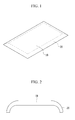
- an exemplary embodiment of the OLED display may include a front display unit 10 that displays an image at a front thereof, and a side display unit 20 that extends from opposite ends of the front display unit 10 and having a bent region.
- the OLED display including the front display unit 10 and the side display unit 20 has no dead space where no image is embodied.
- the color gamut and luminous efficiency are optimized at the front having a viewing angle of about zero (o) degree, while the color purity in the side display unit 20 may be reduced due to the viewing angle.
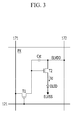
- FIG. 3 is an equivalent circuit diagram showing a pixel of an exemplary embodiment of the OLED display, according to the invention.
- the OLED display includes a plurality of signal lines 121, 71 and 172, and a plurality of pixels PX, e.g., the front pixel A1 and the side pixel A2 shown in FIG. 4 , connected thereto and arranged substantially in a matrix form.
- the signal lines include a plurality of scan lines 121 for transmitting scan signals (or gate signals), a plurality of data lines 171 for transmitting data signals, and a plurality of driving voltage lines 172 for transmitting a driving voltage ELVDD.
- the scan lines 121 extend substantially in a row direction and are arranged substantially parallel to each other, and the data lines 171 and the driving voltage lines 172 extend substantially in a column direction and are arranged substantially parallel to each other.
- each of the pixels PX includes a switching thin film transistor T1, a driving thin film transistor T2, a storage capacitor Cst and an OLED.
- the switching thin film transistor T1 has a control terminal, an input terminal and an output terminal.
- the control terminal of the switching thin film transistor T1 is connected to a corresponding scan line 121
- the input terminal of the switching thin film transistor T1 is connected to a corresponding data line 171
- the output terminal of the switching thin film transistor T1 is connected to the driving thin film transistor T2.
- the switching thin film transistor T1 transmits a data signal applied to the corresponding data line 171 to the driving thin film transistor T2 in response to a scan signal applied to the corresponding scan line 121.
- the driving thin film transistor T2 has a control terminal, an input terminal, and an output terminal.
- the control terminal of the driving thin film transistor T2 is connected to the switching thin film transistor T1
- the input terminal of the driving thin film transistor T2 is connected to the corresponding driving voltage line 172
- the output terminal of the driving thin film transistor T2 is connected to the OLED.
- the driving thin film transistor T2 generates an output current Id that flows to the OLED, and amplitude of the current varies in accordance with a voltage applied between the control terminal and the output terminal of the driving thin film transistor T2.
- the storage capacitor Cst is connected between the control terminal and input terminal of the driving thin film transistor T2.
- the storage capacitor Cst charges a data signal applied to the control terminal of the driving thin film transistor T2, and maintains the data signal after the switching thin film transistor T1 is turned off.
- the OLED has an anode connected to the output terminal of the driving thin film transistor T2 and a cathode connected to a common voltage ELVSS.
- the OLED displays an image by emitting light with various intensities according to the output current Id from the driving thin film transistor T2.
- the switching thin film transistor T1 and the driving thin film transistor T2 may be n-channel field effect transistors ("FET"s) or p-channel FETs.
- connection relationship among the thin film transistors T1 and T2, the storage capacitor Cst, and the OLED may be variously modified. Structures of the front pixel A1 and the side pixel A2 of the OLED display of FIG. 3 will now be described in greater detail with reference to FIG. 4 to FIG. 6 as well as FIG. 3 .
- FIG. 4 is a plan view of a front pixel A1 and a side pixel A2, which are respectively located in a front display unit and a side display unit of an exemplary embodiment of the OLED display, according to the invention.
- FIG. 5 is a cross-sectional view taken along line V-V of the OLED display of FIG. 4 .
- FIG. 6 is cross-sectional view taken along line VI-VI of the OLED display of FIG. 4 .
- FIG. 7 is a CIE xy chromaticity diagram according to thickness of common electrodes of the front pixel A1 and the side pixel A2 of an exemplary embodiment of the OLED display, according to the invention.
- a buffer layer 120 is disposed on a substrate 110 of the front pixel A1 and the side pixel A2.
- the substrate 110 may be an insulating substrate including glass, quartz, ceramic, or plastic, for example.
- the buffer layer 120 effectively prevents contaminants such as impure elements or moisture from intruding into inside of the OLED display, and has a planarized surface.
- the buffer layer 120 may have a single-layered structure of a silicon nitride (SiNx), or a double-layered structure of a silicon nitride (SiNx) and a silicon oxide (SiOx), for example.
- a switching semiconductor layer 135a and a driving semiconductor layer 135b are disposed on the buffer layer 120, and the switching semiconductor layer 135a and the driving semiconductor layer 135b are spaced apart from each other.
- the switching and driving semiconductor layers 135a and 135b may include polysilicon or an oxide semiconductor, for example.
- the oxide semiconductor may include an oxide based on titanium (Ti), hafnium (Hf), zirconium (Zr), aluminum (Al), tantalum (Ta), germanium (Ge), zinc (Zn), gallium (Ga), tin (Sn) or indium (In), or a complex oxide thereof, for example, zinc oxide (ZnO), indium-gallium-zinc oxide (InGaZnO 4 ), indium-zinc oxide (Zn-In-O), zinc-tin oxide (Zn-Sn-O), indium-gallium oxide (In-Ga-O), indium-tin oxide (In-Sn-O), indium-zirconium oxide (In-Zr-O), indium-zirconium-zinc oxide (In-Zr-Zn-O), indium-zirconium-tin oxide (In-Zr-Sn-O), indium-zirconium-tin oxide (In-Zr-Sn-O), indium-zir
- a separate protective layer may be included to protect the oxide semiconductor from an outside environment such as a high temperature.
- Each of the semiconductor layers 135a and 135b includes a channel region, which is not doped with impurities, and source and drain regions, which are doped with impurities and disposed at opposing sides of the channel region.
- the impurities vary according to the type of thin film transistors, and may be N-type impurities or P-type impurities.
- each of the switching semiconductor layer 135a and the driving semiconductor layer 135b is divided into a channel region 1355, and a source region 1356 and a drain region 1357 disposed at opposing sides of the channel region 1355.
- the channel regions 1355 of the switching semiconductor layer 135a and the driving semiconductor layer 135b may include polysilicon, which is not doped with impurities, that is, intrinsic semiconductors, and the source regions 1356 and drain regions 1357 of the switching semiconductor layer 135a and the driving semiconductor layer 135b may include polysilicon, which is doped with conductive impurities, that is, impurity (extrinsic) semiconductors.
- a gate insulating film 140 is disposed on the switching semiconductor layer 135a and the driving semiconductor layer 135b.
- the gate insulating film 140 may include a silicon nitride or a silicon oxide, for example, and may have a single-layer structure or a multi-layer structure.
- a scan line 121, a driving gate electrode 125b and a first storage capacitor plate 128 are disposed on the gate insulating film 140.
- the scan line 121 extends substantially in a horizontal direction and transfers a scan signal, and includes a switching gate electrode 125a that protrudes from the scan line 121 toward the switching semiconductor layer 135a.
- a driving gate electrode 125b protrudes from the first storage capacitor plate 128 toward the driving semiconductor layer 135b.
- the switching gate electrode 125a and the driving gate electrode 125b overlap the channel regions 1355, respectively.
- An interlayer insulating film 160 is disposed on the scan line 121, the driving gate electrode 125b and a first storage capacitor plate 128.
- the interlayer insulating film 160 may include a silicon nitride or a silicon oxide, for example.
- Source contact holes 61 and drain contact holes 62 are defined in the interlayer insulating film 160 and the gate insulating film 140 to expose the source regions 1356 and the drain regions 1357, and storage contact holes 63 are defined in the interlayer insulating film 160 and the gate insulating film 140 to expose part of the first storage capacitor plate 128.
- a data line 171 including a switching source electrode 176a, a driving voltage line 172 including a driving source electrode 176b and a second storage capacitor plate 178, and a switching drain electrode 177a and a driving drain electrode 177b that are connected to the first storage capacitor plate 128 are disposed on the interlayer insulating film 160.
- the data line 171 transfers a data signal and extends substantially in a direction crossing the gate line 121.
- the driving voltage line 172 transfers a driving voltage, and is spaced apart from the data line 171 and extends substantially in the same direction as the data line 171.
- the switching source electrode 176a protrudes from the data line 171 toward the switching semiconductor layer 135a, and the driving source electrode 176b protrudes from the driving voltage line 172 toward the driving semiconductor layer 135b.
- the switching source electrode 176a and the driving source electrode 176b are respectively connected to the source regions 1356 through the source contact holes 61.
- the switching drain electrode 177a faces the switching source electrode 176a
- the driving drain electrode 177b faces the driving source electrode 176b
- the switching drain electrode 177a and the driving drain electrode 177b are respectively connected to the drain regions 1357 through the drain contact holes 62.
- the switching drain electrode 177a is extended toward the first storage capacitor plate 128 and electrically connected to the first storage capacitor plate 128 and the driving gate electrode 125b through the storage contact hole 63 defined in the interlayer insulating film 160.
- the second storage capacitor plate 178 protrudes from the driving voltage line 172, and overlaps the first storage capacitor plate 128. Accordingly, the first storage capacitor plate 128 and the second storage capacitor plate 178 collectively define the storage capacitor Cst with the interlayer insulating film 160, which is disposed therebetween, as a dielectric material.
- the switching semiconductor layer 135a, the switching gate electrode 125a, the switching source electrode 176a and the switching drain electrode 177a collectively define the switching thin film transistor T1
- the driving semiconductor layer 135b, the driving gate electrode 125b, the driving source electrode 176b and the driving drain electrode 177b collectively define the driving thin film transistor T2.
- a protective layer 180 is disposed on the second storage capacitor plate 178, the switching source electrode 176a, the driving source electrode 176b, the switching drain electrode 177a and the driving drain electrode 177b.
- a pixel electrode 710 is disposed on the protective layer 180 as a first electrode of the OLED display, and the pixel electrode 710 may include a transparent conducting material such as indium tin oxide ("ITO"), indium zinc oxide ("IZO"), zinc oxide ("ZnO") or indium oxide (In 2 O 3 ), for example, or a reflective metal such as lithium (Li), calcium (Ca), lithium fluoride/calcium (LiF/Ca), lithium fluoride/aluminum (LiF/Al), aluminum (Al), silver (Ag), magnesium (Mg) or gold (Au), for example.
- the pixel electrode 710 is electrically connected to the driving drain electrode 177b of the driving thin film transistor T2 through a contact hole 181 defined in the protective layer 180, and functions as an anode of the OLED.
- a pixel definition film 350 is disposed on edge portions of the pixel electrode 710 and the protective layer 180.
- An opening 351 is defined in the pixel definition film 350 to expose the pixel electrode 710.
- the pixel definition film 350 may include a resin such as a polyacrylate resin or a polyimide resin, a silica-based inorganic material, or the like, for example.
- An organic emission layer 720 is disposed in the opening 351 of the pixel definition film 350.
- the organic emission layer 720 includes at least one of a plurality of layers including an emission layer, a hole injection layer (“HIL”), a hole transport layer (“HTL”), an electron transport layer (“ETL”) and an electron injection layer (“EIL”).
- the organic emission layer 720 includes emission layer, the HIL, the HTL, the ETL and the EIL, the HIL may be disposed on the pixel electrode 710, that is, the anode, and the HTL, the emission layer, the ETL, and the EIL may be sequentially stacked on the HIL.
- the organic emission layer 720 may include a red organic emission layer for emitting red light, a green organic emission layer for emitting green light or a blue organic emission layer for emitting blue light, and the red organic emission layer, the green organic emission layer and the blue organic emission layer are respectively formed in red, green and blue pixels, thereby displaying a color image.
- the red organic emission layer, green organic emission layer and blue organic emission layer of the organic emission layer 720 may be laminated on each of the red pixel, green pixel and blue pixel, and a red color filter, a green color filter and a blue color filter may be provided for the red, green and blue pixels, respectively, thereby displaying a color image.
- a white organic emission layer for emitting white light may be disposed in all of the red, green and blue pixels, and a red color filter, a green color filter and a blue color filter may be provided for the red, green and blue pixels, respectively, thereby displaying a color image.
- the pixels include the white organic emission layer and the color filters to display a color image
- a deposition process using a mask for depositing the red, green and blue organic emission layers on the respective pixels, i.e., the red, green and blue pixels may be omitted.
- the white organic emission layer may include a single organic emission layer or a plurality of organic emission layers that are laminated to emit white light.
- a yellow organic emission layer and a blue organic emission layer may be combined to emit white light
- a cyan organic emission layer and a red organic emission layer may be combined to emit white light
- a magenta organic emission layer and a green organic emission layer may be combined to emit white light, for example, but not being limited thereto.
- a common electrode 730 is disposed on the pixel definition film 350 and the organic emission layer 720 as a second electrode of the OLED display.
- the common electrode 730 may function as a cathode of the OLED.
- the common electrode 730 disposed in the side pixel A2 is thinner than the common electrode 730 disposed in the front pixel A1 such that a low resonance (weak resonance) structure or a non-resonance structure is provided in the side pixel A2 by reducing reflectivity and increasing transmittance.
- both of the front pixel A1 and the side pixel A2 have a high resonance (strong resonance) structure, a color shift phenomenon occurs according to a viewing angle thereof, e.g., a white color in a front direction is viewed as a bluish color at a viewing angle of about 60 degrees. Accordingly, in an OLED display where a display unit is bent, the front and side may be respectively viewed as a white color and a bluish color due to the bending angle.
- various methods may be used for adjusting a high or low resonance level.
- thickness of the common electrode 730 of the front pixel A1 and the side pixel A2 is differently set to change reflectivity and a resonance condition according to the reflectivity, thereby reducing color deviation.
- CIE xy chromaticity curves when the thickness of the common electrode 730 is about 70 angstroms ( ⁇ ), about 120 ⁇ , about 140 ⁇ , about 160 ⁇ , and about 200 ⁇ are shown.
- the color deviation is reduced as the thickness of the common electrode 730 decreases.
- the front pixel and the side pixel are effectively compensated to display an image with the maximum color purity independently of the bending angle by configuring the common electrode 730 in the front pixel A1 to have the high resonance structure and the common electrode 730 in the side pixel A2 to have the low resonance structure.
- the common electrode 730 may include a transparent conducting material such as ITO, IZO, zinc oxide (ZnO), or indium oxide (In2O3), for example, or a reflective metal such as lithium (Li), calcium (Ca), lithium fluoride/calcium (LiF/Ca), lithium fluoride/aluminum (LiF/Al), aluminum (Al), silver (Ag), magnesium (Mg), or gold (Au), for example.
- the pixel electrode 710, the organic emission layer 720 and the common electrode 730 collectively define the OLED 70.
- the microcavity condition is changed by controlling the thickness of the common electrode 730 of the front pixel A1 and the side pixel A2, as described above.
- the microcavity condition may be changed by controlling the materials of the common electrode 730 of the front pixel A1 and the side pixel A2.
- FIG. 8 is a graph showing a color coordinate variation depending on a material of a common electrode in an alternative exemplary embodiment of an OLED display, according to the invention.
- the common electrode 730 may include a transparent conducting material such as ITO , IZO, zinc oxide (ZnO), or indium oxide (In 2 O 3 ), for example, or a reflective metal such as lithium (Li), calcium (Ca), lithium fluoride/calcium (LiF/Ca), lithium fluoride/aluminum (LiF/Al), aluminum (Al), silver (Ag), magnesium (Mg) or gold (Au), for example.
- a transparent conducting material such as ITO , IZO, zinc oxide (ZnO), or indium oxide (In 2 O 3
- a reflective metal such as lithium (Li), calcium (Ca), lithium fluoride/calcium (LiF/Ca), lithium fluoride/aluminum (LiF/Al), aluminum (Al), silver (Ag), magnesium (Mg) or gold (Au), for example.
- the common electrode of the front pixel may include a material having higher reflectivity than a material of the common electrode of the side pixel.
- the common electrode of the side pixel may include a material having a lower color deviation than a material of the common electrode of the front pixel
- FIG. 8 the change of color coordinates obtained when the common electrode is made of AgMg (where Ag:Mg is about 9:1) and MgAg (where Mg:Ag is about 9:1) is shown.
- ⁇ x in the x-coordinate and ⁇ y in the y-coordinate indicate color deviations of light incident thereto in a color coordinate.
- a color deviation of the common electrode made of AgMg (where Ag:Mg is about 9:1) is less than a color deviation of the common electrode made of MgAg (where Mg:Ag is about 9:1).
- the front display unit and the side display unit may have the high resonance structure and the low resonance structure by configuring the common electrode of the side pixel with AgMg (Ag:Mg is 9:1) having the smaller color deviation and the common electrode of the front pixel with MgAg (Mg:Ag is 9:1) having the larger color deviation. Accordingly, in such an embodiment, the front pixel and the side pixel are effectively compensated to display an image with the maximum color purity independently of the bending angle.
- the common electrodes of the front and side pixels may include various materials to configure the common electrode of the side pixel with a material having a relatively small color deviation and the common electrode of the front pixel with another material having a relatively large color deviation.
- an OLED display has improved visibility at a bent region.
Landscapes
- Physics & Mathematics (AREA)
- Engineering & Computer Science (AREA)
- Microelectronics & Electronic Packaging (AREA)
- Optics & Photonics (AREA)
- Geometry (AREA)
- Electroluminescent Light Sources (AREA)
- Devices For Indicating Variable Information By Combining Individual Elements (AREA)
Abstract
Description
- The described technology relates generally to an organic light emitting diode ("OLED") display.
- An organic light emitting diode ("OLED") display typically includes two electrodes and an organic light emitting member disposed therebetween. Electrons injected from one of the two electrodes and holes injected from the other of the two electrodes are combined in the organic light emitting member to form excitons, and light is emitted from the organic light emitting member as the excitons release energy.
- For applying the OLED display to various types of applications, a flexible OLED display which can be easily flexible has been manufactured. Among the flexible OLED display, a bendable OLED display has a structure including a front display unit embodied to have no dead space even when it is bent at an edge of the front display unit and a side display unit which is visible from the side.
- A bottom light emission type of OLED display, in which light emitted from an organic material is downwardly transferred to a positive electrode, has a smaller color gamut and lower luminous efficiency than those of a top light emission type of OLED display, in which the light is transferred to a negative electrode. Accordingly, a microcavity structure may be applied to the bottom light emission type of OLED display.
- By applying the microcavity structure, light beams are repeatedly reflected between a reflection layer and a transflective layer to generate a strong interference effect such that light beams having a specific wavelength range are amplified while other light beams are offset. The OLED display, to which the microcavity structure is applied, has high color purity at the front.
- The viewing angle characteristic at the side of the OLED display, to which the microcavity structure is applied, is substantially reversely proportional to the viewing angle characteristic at the front thereof. That is, the color purity is reduced.
- When an additional optical film is provided in a predetermined position, or an additional structure is provided below the OLED display to compensate the reduced color purity, manufacturing cost may be increased, and production yield may be reduced.
- Exemplary embodiments of the invention provide an organic light emitting diode ("OLED") display having different color characteristic without using an additional structure by applying a low resonance structure to a bent region, thereby improving visibility.
- An exemplary embodiment provides an OLED display including: a front display unit including a plurality of front pixels disposed on a substrate, where the front pixels display an image on a front surface thereof; and a side display unit including a plurality of side pixels, where the side pixels display an image on a side surface thereof, where the front display unit and the side display unit are configured to have different resonance structures from each other.
- In an exemplary embodiment, the front display unit may have a high resonance structure, and the side display unit may have a low resonance structure.
- In an exemplary embodiment, each of the front pixels and the side pixels may include: a plurality of thin film transistors disposed on the substrate; a protective layer configured to cover the thin film transistors; a first electrode disposed on the protective layer; a pixel definition film disposed on the first electrode, where an opening, which exposes the first electrode on the protective layer, is defined through the pixel definition film; an organic emission layer disposed on the first electrode and in the opening of the pixel definition film; and a second electrode configured to cover the organic emission layer, where the second electrode of the side pixels may be thinner than the second electrode of the front pixels.
- In an exemplary embodiment, the side display unit may have a thickness which decreases as it goes from the front display unit to an end portion of the side display unit.
- In an exemplary embodiment, each of the front pixels and the side pixels may include: a plurality of thin film transistors disposed on the substrate; a protective layer configured to cover the thin film transistors; a first electrode formed on the protective layer; a pixel definition film having an opening which exposes the first electrode formed on the protective layer; an organic emission layer formed on the first electrode and the pixel definition film; and a second electrode configured to cover the organic emission layer, where the second electrode of the front pixel may include a material having higher reflectivity than a material of the second electrode of the side pixel.
- In an exemplary embodiment, each of the front pixels and the side pixels may include: a plurality of thin film transistors disposed on the substrate; a protective layer configured to cover the thin film transistors; a first electrode disposed on the protective layer; a pixel definition film disposed on the first electrode, where an opening, which exposes the first electrode on the protective layer, is defined through the pixel definition film; an organic emission layer disposed on the first electrode and in the opening of the pixel definition film; and a second electrode configured to cover the organic emission layer, where the second electrode of the side pixel may include a material having a lower color deviation than a material of the second electrode of the front pixel.
- In the exemplary embodiments described herein, an OLED display has improved visibility at a bent region.
- The above and other features of the invention will become more apparent by describing in detail exemplary embodiments thereof with reference to the accompanying drawings, in which:
-
FIG. 1 is a perspective of an exemplary embodiment of an organic light emitting diode ("OLED") display, according to the invention. -
FIG. 2 is a side view of an exemplary embodiment of the OLED display, according to the invention. -
FIG. 3 is an equivalent circuit diagram showing a pixel of an exemplary embodiment of the OLED display, according to the invention. -
FIG. 4 is a plan view showing a front pixel A1 and a side pixel A2, which are respectively located in a front display unit and a side display unit of an exemplary embodiment of the OLED display, according to the invention. -
FIG. 5 is a cross-sectional view taken along line V-V of the OLED display ofFIG. 4 . -
FIG. 6 is cross-sectional view taken along line VI-VI of the OLED display ofFIG. 4 . -
FIG. 7 is a CIE xy chromaticity diagram according to thickness of common electrodes of the front pixel A1 and the side pixel A2 of an exemplary embodiment of the OLED display, according to the invention. -
FIG. 8 is a graph showing a color coordinate variation depending on a material of a common electrode in an alternative exemplary embodiment of an OLED display, according to the invention. - In the accompanying drawings, exemplary embodiments, where an organic light emitting diode ("OLED") display is a two transistor-one capacitor ("2Tr-1Cap") structured active matrix ("AM") type of OLED, in which a pixel includes two thin film transistors ("TFT") and one capacitor, are illustrated. However, the invention is not limited thereto. In an alternative exemplary embodiment, an OLED display may have various structures, in which a pixel may include a plurality of TFTs and a capacitor, a wiring line may be further provided, and a conventional wiring line may be omitted.
- Herein, a pixel refers to a minimum unit that displays an image, and an OLED display displays an image through a plurality of pixels.
- As shown in
FIG. 1 and FIG. 2 , an exemplary embodiment of the OLED display may include afront display unit 10 that displays an image at a front thereof, and aside display unit 20 that extends from opposite ends of thefront display unit 10 and having a bent region. - In such an embodiment, the OLED display including the
front display unit 10 and theside display unit 20 has no dead space where no image is embodied. - However, as shown in
FIG. 2 , in thefront display unit 10, the color gamut and luminous efficiency are optimized at the front having a viewing angle of about zero (o) degree, while the color purity in theside display unit 20 may be reduced due to the viewing angle. - The structures of an exemplary embodiment of the OLED display, where front pixels A1 and side pixels A2 respectively disposed in the
front display unit 10 and theside display unit 20 to allow theside display unit 20 to have maximum color purity at a predetermined viewing angle, will be described with reference toFIG. 3 to FIG. 5 . -
FIG. 3 is an equivalent circuit diagram showing a pixel of an exemplary embodiment of the OLED display, according to the invention. - In such an embodiment, as shown in
FIG. 3 , the OLED display includes a plurality ofsignal lines FIG. 4 , connected thereto and arranged substantially in a matrix form. - The signal lines include a plurality of
scan lines 121 for transmitting scan signals (or gate signals), a plurality ofdata lines 171 for transmitting data signals, and a plurality ofdriving voltage lines 172 for transmitting a driving voltage ELVDD. - Referring to
FIG. 3 , thescan lines 121 extend substantially in a row direction and are arranged substantially parallel to each other, and thedata lines 171 and thedriving voltage lines 172 extend substantially in a column direction and are arranged substantially parallel to each other. - In an exemplary embodiment, each of the pixels PX includes a switching thin film transistor T1, a driving thin film transistor T2, a storage capacitor Cst and an OLED.
- The switching thin film transistor T1 has a control terminal, an input terminal and an output terminal. The control terminal of the switching thin film transistor T1 is connected to a
corresponding scan line 121, the input terminal of the switching thin film transistor T1 is connected to acorresponding data line 171, and the output terminal of the switching thin film transistor T1 is connected to the driving thin film transistor T2. The switching thin film transistor T1 transmits a data signal applied to thecorresponding data line 171 to the driving thin film transistor T2 in response to a scan signal applied to thecorresponding scan line 121. - The driving thin film transistor T2 has a control terminal, an input terminal, and an output terminal. The control terminal of the driving thin film transistor T2 is connected to the switching thin film transistor T1, the input terminal of the driving thin film transistor T2 is connected to the corresponding
driving voltage line 172, and the output terminal of the driving thin film transistor T2 is connected to the OLED. The driving thin film transistor T2 generates an output current Id that flows to the OLED, and amplitude of the current varies in accordance with a voltage applied between the control terminal and the output terminal of the driving thin film transistor T2. - The storage capacitor Cst is connected between the control terminal and input terminal of the driving thin film transistor T2. The storage capacitor Cst charges a data signal applied to the control terminal of the driving thin film transistor T2, and maintains the data signal after the switching thin film transistor T1 is turned off.
- The OLED has an anode connected to the output terminal of the driving thin film transistor T2 and a cathode connected to a common voltage ELVSS. The OLED displays an image by emitting light with various intensities according to the output current Id from the driving thin film transistor T2.
- The switching thin film transistor T1 and the driving thin film transistor T2 may be n-channel field effect transistors ("FET"s) or p-channel FETs.
- In an alternative exemplary embodiment, the connection relationship among the thin film transistors T1 and T2, the storage capacitor Cst, and the OLED may be variously modified. Structures of the front pixel A1 and the side pixel A2 of the OLED display of
FIG. 3 will now be described in greater detail with reference toFIG. 4 to FIG. 6 as well asFIG. 3 . -
FIG. 4 is a plan view of a front pixel A1 and a side pixel A2, which are respectively located in a front display unit and a side display unit of an exemplary embodiment of the OLED display, according to the invention.FIG. 5 is a cross-sectional view taken along line V-V of the OLED display ofFIG. 4 .FIG. 6 is cross-sectional view taken along line VI-VI of the OLED display ofFIG. 4 .FIG. 7 is a CIE xy chromaticity diagram according to thickness of common electrodes of the front pixel A1 and the side pixel A2 of an exemplary embodiment of the OLED display, according to the invention. - As shown in
FIG. 4 to FIG. 6 , in an exemplary embodiment of the OLED display, abuffer layer 120 is disposed on asubstrate 110 of the front pixel A1 and the side pixel A2. - The
substrate 110 may be an insulating substrate including glass, quartz, ceramic, or plastic, for example. - The
buffer layer 120 effectively prevents contaminants such as impure elements or moisture from intruding into inside of the OLED display, and has a planarized surface. - The
buffer layer 120 may have a single-layered structure of a silicon nitride (SiNx), or a double-layered structure of a silicon nitride (SiNx) and a silicon oxide (SiOx), for example. - A
switching semiconductor layer 135a and a drivingsemiconductor layer 135b are disposed on thebuffer layer 120, and the switchingsemiconductor layer 135a and thedriving semiconductor layer 135b are spaced apart from each other. The switching and drivingsemiconductor layers - The oxide semiconductor may include an oxide based on titanium (Ti), hafnium (Hf), zirconium (Zr), aluminum (Al), tantalum (Ta), germanium (Ge), zinc (Zn), gallium (Ga), tin (Sn) or indium (In), or a complex oxide thereof, for example, zinc oxide (ZnO), indium-gallium-zinc oxide (InGaZnO4), indium-zinc oxide (Zn-In-O), zinc-tin oxide (Zn-Sn-O), indium-gallium oxide (In-Ga-O), indium-tin oxide (In-Sn-O), indium-zirconium oxide (In-Zr-O), indium-zirconium-zinc oxide (In-Zr-Zn-O), indium-zirconium-tin oxide (In-Zr-Sn-O), indium-zirconium-gallium oxide (In-Zr-Ga-O), indium-aluminum oxide (In-Al-O), indium-zinc-aluminum oxide (In-Zn-Al-O), indium-tin-aluminum oxide (In-Sn-Al-O), indium-aluminum-gallium oxide (In-Al-Ga-O), indium-tantalum oxide (In-Ta-O), indium-tantalum-zinc oxide (In-Ta-Zn-O), indium-tantalum-tin oxide (In-Ta-Sn-O), indium-tantalum-gallium oxide (In-Ta-Ga-O), indium-germanium oxide (In-Ge-O), indium-germanium-zinc oxide (In-Ge-Zn-O), indium-germanium-tin oxide (In-Ge-Sn-O), indium-germanium-gallium oxide (In-Ge-Ga-O), titanium-indium-zinc oxide (Ti-In-Zn-O) or hafnium-indium-zinc oxide (Hf-In-Zn-O).
- In an exemplary embodiment, where the
semiconductor layers - Each of the
semiconductor layers - In such an embodiment, as shown in
FIGS. 5 and6 , each of the switchingsemiconductor layer 135a and the drivingsemiconductor layer 135b is divided into achannel region 1355, and asource region 1356 and adrain region 1357 disposed at opposing sides of thechannel region 1355. Thechannel regions 1355 of the switchingsemiconductor layer 135a and the drivingsemiconductor layer 135b may include polysilicon, which is not doped with impurities, that is, intrinsic semiconductors, and thesource regions 1356 anddrain regions 1357 of the switchingsemiconductor layer 135a and the drivingsemiconductor layer 135b may include polysilicon, which is doped with conductive impurities, that is, impurity (extrinsic) semiconductors. - In such an embodiment, a
gate insulating film 140 is disposed on the switchingsemiconductor layer 135a and the drivingsemiconductor layer 135b. Thegate insulating film 140 may include a silicon nitride or a silicon oxide, for example, and may have a single-layer structure or a multi-layer structure. - A
scan line 121, a drivinggate electrode 125b and a firststorage capacitor plate 128 are disposed on thegate insulating film 140. Thescan line 121 extends substantially in a horizontal direction and transfers a scan signal, and includes a switchinggate electrode 125a that protrudes from thescan line 121 toward the switchingsemiconductor layer 135a. A drivinggate electrode 125b protrudes from the firststorage capacitor plate 128 toward the drivingsemiconductor layer 135b. The switchinggate electrode 125a and the drivinggate electrode 125b overlap thechannel regions 1355, respectively. - An interlayer insulating
film 160 is disposed on thescan line 121, the drivinggate electrode 125b and a firststorage capacitor plate 128. In such an embodiment, theinterlayer insulating film 160 may include a silicon nitride or a silicon oxide, for example. - Source contact holes 61 and drain contact holes 62 are defined in the
interlayer insulating film 160 and thegate insulating film 140 to expose thesource regions 1356 and thedrain regions 1357, and storage contact holes 63 are defined in theinterlayer insulating film 160 and thegate insulating film 140 to expose part of the firststorage capacitor plate 128. - A
data line 171 including aswitching source electrode 176a, a drivingvoltage line 172 including a drivingsource electrode 176b and a secondstorage capacitor plate 178, and aswitching drain electrode 177a and a drivingdrain electrode 177b that are connected to the firststorage capacitor plate 128 are disposed on theinterlayer insulating film 160. - The
data line 171 transfers a data signal and extends substantially in a direction crossing thegate line 121. The drivingvoltage line 172 transfers a driving voltage, and is spaced apart from thedata line 171 and extends substantially in the same direction as thedata line 171. - The switching
source electrode 176a protrudes from thedata line 171 toward the switchingsemiconductor layer 135a, and the drivingsource electrode 176b protrudes from the drivingvoltage line 172 toward the drivingsemiconductor layer 135b. The switchingsource electrode 176a and the drivingsource electrode 176b are respectively connected to thesource regions 1356 through the source contact holes 61. The switchingdrain electrode 177a faces the switchingsource electrode 176a, the drivingdrain electrode 177b faces the drivingsource electrode 176b, and theswitching drain electrode 177a and the drivingdrain electrode 177b are respectively connected to thedrain regions 1357 through the drain contact holes 62. - The switching
drain electrode 177a is extended toward the firststorage capacitor plate 128 and electrically connected to the firststorage capacitor plate 128 and the drivinggate electrode 125b through thestorage contact hole 63 defined in theinterlayer insulating film 160. - The second
storage capacitor plate 178 protrudes from the drivingvoltage line 172, and overlaps the firststorage capacitor plate 128. Accordingly, the firststorage capacitor plate 128 and the secondstorage capacitor plate 178 collectively define the storage capacitor Cst with theinterlayer insulating film 160, which is disposed therebetween, as a dielectric material. - The switching
semiconductor layer 135a, the switchinggate electrode 125a, the switchingsource electrode 176a and theswitching drain electrode 177a collectively define the switching thin film transistor T1, and the drivingsemiconductor layer 135b, the drivinggate electrode 125b, the drivingsource electrode 176b and the drivingdrain electrode 177b collectively define the driving thin film transistor T2. - A
protective layer 180 is disposed on the secondstorage capacitor plate 178, the switchingsource electrode 176a, the drivingsource electrode 176b, the switchingdrain electrode 177a and the drivingdrain electrode 177b. - A
pixel electrode 710 is disposed on theprotective layer 180 as a first electrode of the OLED display, and thepixel electrode 710 may include a transparent conducting material such as indium tin oxide ("ITO"), indium zinc oxide ("IZO"), zinc oxide ("ZnO") or indium oxide (In2O3), for example, or a reflective metal such as lithium (Li), calcium (Ca), lithium fluoride/calcium (LiF/Ca), lithium fluoride/aluminum (LiF/Al), aluminum (Al), silver (Ag), magnesium (Mg) or gold (Au), for example. Thepixel electrode 710 is electrically connected to the drivingdrain electrode 177b of the driving thin film transistor T2 through acontact hole 181 defined in theprotective layer 180, and functions as an anode of the OLED. - A
pixel definition film 350 is disposed on edge portions of thepixel electrode 710 and theprotective layer 180. Anopening 351 is defined in thepixel definition film 350 to expose thepixel electrode 710. - In an exemplary embodiment, the
pixel definition film 350 may include a resin such as a polyacrylate resin or a polyimide resin, a silica-based inorganic material, or the like, for example. - An
organic emission layer 720 is disposed in theopening 351 of thepixel definition film 350. - The
organic emission layer 720 includes at least one of a plurality of layers including an emission layer, a hole injection layer ("HIL"), a hole transport layer ("HTL"), an electron transport layer ("ETL") and an electron injection layer ("EIL"). In an exemplary embodiment, theorganic emission layer 720 includes emission layer, the HIL, the HTL, the ETL and the EIL, the HIL may be disposed on thepixel electrode 710, that is, the anode, and the HTL, the emission layer, the ETL, and the EIL may be sequentially stacked on the HIL. - In an exemplary embodiment, the
organic emission layer 720 may include a red organic emission layer for emitting red light, a green organic emission layer for emitting green light or a blue organic emission layer for emitting blue light, and the red organic emission layer, the green organic emission layer and the blue organic emission layer are respectively formed in red, green and blue pixels, thereby displaying a color image. - In an alternative exemplary embodiment, the red organic emission layer, green organic emission layer and blue organic emission layer of the
organic emission layer 720 may be laminated on each of the red pixel, green pixel and blue pixel, and a red color filter, a green color filter and a blue color filter may be provided for the red, green and blue pixels, respectively, thereby displaying a color image. - In another alternative exemplary embodiment, a white organic emission layer for emitting white light may be disposed in all of the red, green and blue pixels, and a red color filter, a green color filter and a blue color filter may be provided for the red, green and blue pixels, respectively, thereby displaying a color image. In such an embodiment, where the pixels include the white organic emission layer and the color filters to display a color image, a deposition process using a mask for depositing the red, green and blue organic emission layers on the respective pixels, i.e., the red, green and blue pixels may be omitted.
- In such an embodiment, the white organic emission layer may include a single organic emission layer or a plurality of organic emission layers that are laminated to emit white light. In such an embodiment, a yellow organic emission layer and a blue organic emission layer may be combined to emit white light, a cyan organic emission layer and a red organic emission layer may be combined to emit white light, or a magenta organic emission layer and a green organic emission layer may be combined to emit white light, for example, but not being limited thereto.
- A
common electrode 730 is disposed on thepixel definition film 350 and theorganic emission layer 720 as a second electrode of the OLED display. In an exemplary embodiment, thecommon electrode 730 may function as a cathode of the OLED. - In an exemplary embodiment, as shown in
FIG. 5 andFIG. 6 , thecommon electrode 730 disposed in the side pixel A2 is thinner than thecommon electrode 730 disposed in the front pixel A1 such that a low resonance (weak resonance) structure or a non-resonance structure is provided in the side pixel A2 by reducing reflectivity and increasing transmittance. - When both of the front pixel A1 and the side pixel A2 have a high resonance (strong resonance) structure, a color shift phenomenon occurs according to a viewing angle thereof, e.g., a white color in a front direction is viewed as a bluish color at a viewing angle of about 60 degrees. Accordingly, in an OLED display where a display unit is bent, the front and side may be respectively viewed as a white color and a bluish color due to the bending angle.
- In an exemplary embodiment of the invention, various methods may be used for adjusting a high or low resonance level. In an exemplary embodiment of the OLED display, thickness of the
common electrode 730 of the front pixel A1 and the side pixel A2 is differently set to change reflectivity and a resonance condition according to the reflectivity, thereby reducing color deviation. - In
FIG. 7 , CIE xy chromaticity curves when the thickness of thecommon electrode 730 is about 70 angstroms (Å), about 120 Å, about 140 Å, about 160 Å, and about 200 Å are shown. - As shown in
FIG. 7 , the color deviation is reduced as the thickness of thecommon electrode 730 decreases. - Accordingly, in such an embodiment, the front pixel and the side pixel are effectively compensated to display an image with the maximum color purity independently of the bending angle by configuring the
common electrode 730 in the front pixel A1 to have the high resonance structure and thecommon electrode 730 in the side pixel A2 to have the low resonance structure. - The
common electrode 730 may include a transparent conducting material such as ITO, IZO, zinc oxide (ZnO), or indium oxide (In2O3), for example, or a reflective metal such as lithium (Li), calcium (Ca), lithium fluoride/calcium (LiF/Ca), lithium fluoride/aluminum (LiF/Al), aluminum (Al), silver (Ag), magnesium (Mg), or gold (Au), for example.
Thepixel electrode 710, theorganic emission layer 720 and thecommon electrode 730 collectively define theOLED 70. - In an exemplary embodiment of the OLED display, the microcavity condition is changed by controlling the thickness of the
common electrode 730 of the front pixel A1 and the side pixel A2, as described above. In an alternative exemplary embodiment, the microcavity condition may be changed by controlling the materials of thecommon electrode 730 of the front pixel A1 and the side pixel A2. -
FIG. 8 is a graph showing a color coordinate variation depending on a material of a common electrode in an alternative exemplary embodiment of an OLED display, according to the invention. - In such an embodiment, as described above, the
common electrode 730 may include a transparent conducting material such as ITO , IZO, zinc oxide (ZnO), or indium oxide (In2O3), for example, or a reflective metal such as lithium (Li), calcium (Ca), lithium fluoride/calcium (LiF/Ca), lithium fluoride/aluminum (LiF/Al), aluminum (Al), silver (Ag), magnesium (Mg) or gold (Au), for example. - In an exemplary embodiment, the common electrode of the front pixel may include a material having higher reflectivity than a material of the common electrode of the side pixel. In an alternative exemplary embodiment, the common electrode of the side pixel may include a material having a lower color deviation than a material of the common electrode of the front pixel
- In
FIG. 8 , the change of color coordinates obtained when the common electrode is made of AgMg (where Ag:Mg is about 9:1) and MgAg (where Mg:Ag is about 9:1) is shown. - In
FIG. 8 , Δx in the x-coordinate and Δy in the y-coordinate indicate color deviations of light incident thereto in a color coordinate. - As shown in
FIG. 8 , a color deviation of the common electrode made of AgMg (where Ag:Mg is about 9:1) is less than a color deviation of the common electrode made of MgAg (where Mg:Ag is about 9:1). - To decrease the color deviation in the bent region, e.g., the side pixel, the front display unit and the side display unit may have the high resonance structure and the low resonance structure by configuring the common electrode of the side pixel with AgMg (Ag:Mg is 9:1) having the smaller color deviation and the common electrode of the front pixel with MgAg (Mg:Ag is 9:1) having the larger color deviation. Accordingly, in such an embodiment, the front pixel and the side pixel are effectively compensated to display an image with the maximum color purity independently of the bending angle.
- In such an embodiment, the common electrodes of the front and side pixels may include various materials to configure the common electrode of the side pixel with a material having a relatively small color deviation and the common electrode of the front pixel with another material having a relatively large color deviation.
- In the exemplary embodiments of the invention, as described herein, an OLED display has improved visibility at a bent region.
- While the invention has been described in connection with what is presently considered to be practical exemplary embodiments, it is to be understood that the invention is not limited to the disclosed embodiments, but, on the contrary, is intended to cover various modifications and equivalent arrangements included within the scope of the appended claims.
Claims (6)
- An organic light emitting diode display comprising:a front display unit comprising a plurality of front pixels disposed on a substrate, wherein the front pixels display an image on a front surface thereof; anda side display unit comprising a plurality of side pixels disposed on the substrate, wherein the side pixels display an image on a side surface thereof,wherein the front display unit and the side display unit are configured to have different resonance structures from each other.
- The organic light emitting diode display of claim 1, wherein
the front display unit has a high resonance structure, and
the side display unit has a low resonance structure. - The organic light emitting diode display of claim 2, wherein each of the front pixels and the side pixels comprises:a plurality of thin film transistors disposed on the substrate;a protective layer configured to cover the thin film transistors;a first electrode disposed on the protective layer;a pixel definition film disposed on the first electrode, wherein an opening, which exposes the first electrode on the protective layer, is defined through the pixel definition film;an organic emission layer disposed on the first electrode and in the opening of the pixel definition film; anda second electrode configured to cover the organic emission layer,wherein the second electrode of the side pixels is thinner than the second electrode of the front pixels.
- The organic light emitting diode display of claim 3, wherein the side display unit has a thickness which decreases in a direction from the front display unit to an end portion of the side display unit.
- The organic light emitting diode display of claim 2, 3 or 4, wherein each of the front pixels and the side pixels comprises:a plurality of thin film transistors disposed on the substrate;a protective layer configured to cover the thin film transistors;a first electrode disposed on the protective layer;a pixel definition film disposed on the first electrode, wherein an opening, which exposes the first electrode on the protective layer, is defined through the pixel definition film;an organic emission layer disposed on the first electrode and in the opening of the pixel definition film; anda second electrode configured to cover the organic emission layer,wherein the second electrode of the front pixels comprises a material having higher reflectivity than a material of the second electrode of the side pixels.
- The organic light emitting diode display of claim 2, 3 or 4, wherein each of the front pixels and the side pixels comprises:a plurality of thin film transistors disposed on the substrate;a protective layer configured to cover the thin film transistors;a first electrode formed on the protective layer;a pixel definition film disposed on the first electrode, wherein an opening, which exposes the first electrode on the protective layer, is defined through the pixel definition film;an organic emission layer disposed on the first electrode and in the opening of the pixel definition film; anda second electrode configured to cover the organic emission layer,wherein the second electrode of the side pixels comprises a material having a lower color deviation than a material of the second electrode of the front pixels.
Applications Claiming Priority (1)
| Application Number | Priority Date | Filing Date | Title |
|---|---|---|---|
| KR1020130107953A KR102094391B1 (en) | 2013-09-09 | 2013-09-09 | Organic light emitting diode display |
Publications (2)
| Publication Number | Publication Date |
|---|---|
| EP2846373A2 true EP2846373A2 (en) | 2015-03-11 |
| EP2846373A3 EP2846373A3 (en) | 2015-04-29 |
Family
ID=51355461
Family Applications (1)
| Application Number | Title | Priority Date | Filing Date |
|---|---|---|---|
| EP20140181128 Withdrawn EP2846373A3 (en) | 2013-09-09 | 2014-08-15 | Organic light emitting diode display |
Country Status (4)
| Country | Link |
|---|---|
| US (1) | US9577017B2 (en) |
| EP (1) | EP2846373A3 (en) |
| KR (1) | KR102094391B1 (en) |
| CN (1) | CN104425563B (en) |
Families Citing this family (19)
| Publication number | Priority date | Publication date | Assignee | Title |
|---|---|---|---|---|
| US9516743B2 (en) | 2013-02-27 | 2016-12-06 | Apple Inc. | Electronic device with reduced-stress flexible display |
| KR102215147B1 (en) * | 2014-08-14 | 2021-02-15 | 삼성디스플레이 주식회사 | Organic light emitting diode display |
| US9773853B2 (en) | 2015-01-09 | 2017-09-26 | Apple Inc. | Organic light-emitting diode display with bent substrate |
| KR102369674B1 (en) | 2015-02-17 | 2022-03-04 | 삼성디스플레이 주식회사 | Display device and electric equipment using the same |
| KR102322083B1 (en) | 2015-07-28 | 2021-11-04 | 삼성디스플레이 주식회사 | Organic light emitting diode display and manufacturing method thereof |
| KR102490885B1 (en) | 2015-08-21 | 2023-01-25 | 삼성디스플레이 주식회사 | Display device |
| US9716248B2 (en) | 2015-12-18 | 2017-07-25 | Apple Inc. | Organic light-emitting diode displays with reduced border area |
| KR102717868B1 (en) * | 2016-09-13 | 2024-10-15 | 삼성디스플레이 주식회사 | Display device |
| KR102620018B1 (en) * | 2016-09-30 | 2024-01-02 | 삼성디스플레이 주식회사 | Organic light emitting display device and test method of open short thereof |
| KR102766476B1 (en) * | 2017-01-19 | 2025-02-13 | 삼성디스플레이 주식회사 | Organic light emitting display apparatus |
| JP7029894B2 (en) * | 2017-07-11 | 2022-03-04 | 株式会社ジャパンディスプレイ | Display device |
| CN107482038B (en) * | 2017-08-02 | 2020-11-03 | 京东方科技集团股份有限公司 | OLED display panel and manufacturing method thereof, and OLED display device |
| KR102478513B1 (en) * | 2017-10-11 | 2022-12-16 | 삼성디스플레이 주식회사 | Organic light emitting display device |
| CN108075047B (en) * | 2017-12-11 | 2025-02-25 | 合肥京东方光电科技有限公司 | Organic light emitting diode device and manufacturing method thereof, and display panel |
| KR102713989B1 (en) * | 2018-11-19 | 2024-10-07 | 삼성디스플레이 주식회사 | Display device and manufacturing method thereof |
| CN111816791B (en) * | 2020-08-17 | 2023-10-10 | 京东方科技集团股份有限公司 | Display substrate and display device |
| CN114023762B (en) * | 2021-10-18 | 2023-06-27 | 深圳市华星光电半导体显示技术有限公司 | A kind of array substrate and its preparation method, display panel |
| WO2024127605A1 (en) * | 2022-12-15 | 2024-06-20 | シャープディスプレイテクノロジー株式会社 | Display device and method for producing display device |
| KR20250012011A (en) * | 2023-07-13 | 2025-01-23 | 삼성디스플레이 주식회사 | Display device |
Family Cites Families (13)
| Publication number | Priority date | Publication date | Assignee | Title |
|---|---|---|---|---|
| KR100327495B1 (en) | 2000-05-17 | 2002-03-15 | 윤종용 | Bulk acoustic wave resonators and filters having a frequency trimming coil |
| JP4588603B2 (en) * | 2005-09-30 | 2010-12-01 | 京セラ株式会社 | Electroluminescent device |
| JP5178088B2 (en) | 2006-09-07 | 2013-04-10 | キヤノン株式会社 | Organic light emitting device |
| US20100118522A1 (en) | 2007-05-02 | 2010-05-13 | Koninklijke Philips Electronics N.V. | Light emitting device using oled panels in folded or deployed configuration |
| US20100051973A1 (en) * | 2008-08-28 | 2010-03-04 | Seiko Epson Corporation | Light-emitting device, electronic equipment, and process of producing light-emitting device |
| JP5411469B2 (en) * | 2008-08-28 | 2014-02-12 | セイコーエプソン株式会社 | LIGHT EMITTING DEVICE AND ELECTRONIC DEVICE |
| KR20100037876A (en) * | 2008-10-02 | 2010-04-12 | 삼성전자주식회사 | Organic light emitting display and method of manufacturing the same |
| JP5453952B2 (en) * | 2009-06-23 | 2014-03-26 | ソニー株式会社 | ORGANIC ELECTROLUMINESCENCE ELEMENT AND ITS MANUFACTURING METHOD, DISPLAY DEVICE AND ITS MANUFACTURING METHOD |
| KR101084189B1 (en) * | 2010-01-21 | 2011-11-17 | 삼성모바일디스플레이주식회사 | Organic light emitting display |
| KR101108167B1 (en) | 2010-02-12 | 2012-02-06 | 삼성모바일디스플레이주식회사 | Organic light emitting display device |
| KR101084198B1 (en) * | 2010-02-24 | 2011-11-17 | 삼성모바일디스플레이주식회사 | Organic light emitting display |
| KR101097337B1 (en) * | 2010-03-05 | 2011-12-21 | 삼성모바일디스플레이주식회사 | Organic light emitting display |
| KR101320384B1 (en) * | 2011-06-30 | 2013-10-23 | 삼성디스플레이 주식회사 | Flexible display panel and the display apparatus comprising the flexible display panel |
-
2013
- 2013-09-09 KR KR1020130107953A patent/KR102094391B1/en active Active
-
2014
- 2014-04-23 US US14/259,945 patent/US9577017B2/en active Active
- 2014-08-15 EP EP20140181128 patent/EP2846373A3/en not_active Withdrawn
- 2014-09-09 CN CN201410455066.XA patent/CN104425563B/en active Active
Non-Patent Citations (1)
| Title |
|---|
| None |
Also Published As
| Publication number | Publication date |
|---|---|
| US9577017B2 (en) | 2017-02-21 |
| CN104425563B (en) | 2019-10-11 |
| US20150069341A1 (en) | 2015-03-12 |
| KR102094391B1 (en) | 2020-03-30 |
| EP2846373A3 (en) | 2015-04-29 |
| CN104425563A (en) | 2015-03-18 |
| KR20150029158A (en) | 2015-03-18 |
Similar Documents
| Publication | Publication Date | Title |
|---|---|---|
| US9577017B2 (en) | Organic light emitting diode display | |
| KR102114398B1 (en) | Organic light emitting diode display | |
| KR102060622B1 (en) | Organic light emitting diode display | |
| US10014356B2 (en) | Organic light-emitting diode display | |
| US9893134B2 (en) | Organic light-emitting diode display | |
| KR102072140B1 (en) | Organic light emitting diode display | |
| US9627450B2 (en) | Organic light emitting display device | |
| KR102325191B1 (en) | Display Device | |
| KR102091835B1 (en) | Organic light emitting diode display | |
| US9989820B2 (en) | Display device including flexible printed circuit board | |
| KR102119159B1 (en) | Organic light emitting diode display | |
| KR102435391B1 (en) | Display device | |
| TWI690103B (en) | Organic light emitting diode display | |
| US12439687B2 (en) | Organic light emitting display device and method of manufacturing organic light emitting display device | |
| KR101975957B1 (en) | Organic light emitting diode display | |
| KR20150050706A (en) | Display device | |
| US20150042634A1 (en) | Organic light emitting diode display |
Legal Events
| Date | Code | Title | Description |
|---|---|---|---|
| 17P | Request for examination filed |
Effective date: 20140815 |
|
| AK | Designated contracting states |
Kind code of ref document: A2 Designated state(s): AL AT BE BG CH CY CZ DE DK EE ES FI FR GB GR HR HU IE IS IT LI LT LU LV MC MK MT NL NO PL PT RO RS SE SI SK SM TR |
|
| AX | Request for extension of the european patent |
Extension state: BA ME |
|
| PUAI | Public reference made under article 153(3) epc to a published international application that has entered the european phase |
Free format text: ORIGINAL CODE: 0009012 |
|
| PUAL | Search report despatched |
Free format text: ORIGINAL CODE: 0009013 |
|
| AK | Designated contracting states |
Kind code of ref document: A3 Designated state(s): AL AT BE BG CH CY CZ DE DK EE ES FI FR GB GR HR HU IE IS IT LI LT LU LV MC MK MT NL NO PL PT RO RS SE SI SK SM TR |
|
| AX | Request for extension of the european patent |
Extension state: BA ME |
|
| RIC1 | Information provided on ipc code assigned before grant |
Ipc: H01L 27/32 20060101ALI20150320BHEP Ipc: H01L 51/52 20060101AFI20150320BHEP |
|
| R17P | Request for examination filed (corrected) |
Effective date: 20150731 |
|
| RBV | Designated contracting states (corrected) |
Designated state(s): AL AT BE BG CH CY CZ DE DK EE ES FI FR GB GR HR HU IE IS IT LI LT LU LV MC MK MT NL NO PL PT RO RS SE SI SK SM TR |
|
| RAP1 | Party data changed (applicant data changed or rights of an application transferred) |
Owner name: SAMSUNG DISPLAY CO., LTD. |
|
| STAA | Information on the status of an ep patent application or granted ep patent |
Free format text: STATUS: EXAMINATION IS IN PROGRESS |
|
| 17Q | First examination report despatched |
Effective date: 20190619 |
|
| STAA | Information on the status of an ep patent application or granted ep patent |
Free format text: STATUS: THE APPLICATION IS DEEMED TO BE WITHDRAWN |
|
| 18D | Application deemed to be withdrawn |
Effective date: 20191030 |