EP2846351A2 - Radio frequency characteristics measurement jig device - Google Patents
Radio frequency characteristics measurement jig device Download PDFInfo
- Publication number
- EP2846351A2 EP2846351A2 EP20140177080 EP14177080A EP2846351A2 EP 2846351 A2 EP2846351 A2 EP 2846351A2 EP 20140177080 EP20140177080 EP 20140177080 EP 14177080 A EP14177080 A EP 14177080A EP 2846351 A2 EP2846351 A2 EP 2846351A2
- Authority
- EP
- European Patent Office
- Prior art keywords
- conductive layer
- radio frequency
- ground
- ground conductive
- connection substrate
- Prior art date
- Legal status (The legal status is an assumption and is not a legal conclusion. Google has not performed a legal analysis and makes no representation as to the accuracy of the status listed.)
- Withdrawn
Links
Images


Classifications
-
- G—PHYSICS
- G01—MEASURING; TESTING
- G01R—MEASURING ELECTRIC VARIABLES; MEASURING MAGNETIC VARIABLES
- G01R31/00—Arrangements for testing electric properties; Arrangements for locating electric faults; Arrangements for electrical testing characterised by what is being tested not provided for elsewhere
- G01R31/26—Testing of individual semiconductor devices
- G01R31/2601—Apparatus or methods therefor
-
- H—ELECTRICITY
- H01—ELECTRIC ELEMENTS
- H01L—SEMICONDUCTOR DEVICES NOT COVERED BY CLASS H10
- H01L22/00—Testing or measuring during manufacture or treatment; Reliability measurements, i.e. testing of parts without further processing to modify the parts as such; Structural arrangements therefor
- H01L22/10—Measuring as part of the manufacturing process
- H01L22/14—Measuring as part of the manufacturing process for electrical parameters, e.g. resistance, deep-levels, CV, diffusions by electrical means
-
- G—PHYSICS
- G01—MEASURING; TESTING
- G01R—MEASURING ELECTRIC VARIABLES; MEASURING MAGNETIC VARIABLES
- G01R1/00—Details of instruments or arrangements of the types included in groups G01R5/00 - G01R13/00 and G01R31/00
- G01R1/02—General constructional details
- G01R1/04—Housings; Supporting members; Arrangements of terminals
- G01R1/0408—Test fixtures or contact fields; Connectors or connecting adaptors; Test clips; Test sockets
- G01R1/0433—Sockets for IC's or transistors
- G01R1/0441—Details
- G01R1/045—Sockets or component fixtures for RF or HF testing
Definitions
- Embodiments described herein relate generally a radio frequency characteristics measurement jig device.
- Radio frequency semiconductor devices such as GaN HEMT (high electron mobility transistor) and SiC MESFET (metal semiconductor field effect transistor) can provide high power at radio frequencies.
- GaN HEMT high electron mobility transistor
- SiC MESFET metal semiconductor field effect transistor
- Radio frequency semiconductor devices and MMIC are connected to microstrip lines to constitute an electronic device.
- radio frequency semiconductor devices and MMIC are preferably mounted in a package with reduced parasitic capacitance and parasitic inductance.
- the efficiency of the assembly process can be improved by screening radio frequency devices satisfying the required specifications and incorporating them in the electronic device.
- a measurement device capable of measuring radio frequency characteristics with high accuracy in a short time.
- a radio frequency characteristics measurement jig device includes: a ground conductor part; a first coplanar line; a connection substrate; and a holding part.
- the radio frequency characteristics measurement jig device is used to measure a radio frequency device including a signal terminal.
- the first coplanar line includes a first dielectric layer provided on a surface of the ground conductor part, a first center conductive layer provided on a surface of the first dielectric layer, and first ground conductive layers respectively provided outside first gaps provided on both sides of the first center conductive layer on the surface of the first dielectric layer.
- the connection substrate includes a second dielectric layer having a first surface and a second surface on an opposite side from of the first surface, a second center conductive layer provided on the first surface, second ground conductive layers respectively provided outside second gaps provided on both sides of the second center conductive layer, and a third ground conductive layer provided on the second surface and connected to the second ground conductive layer.
- the second dielectric layer includes a first region provided with the second center conductive layer and the second ground conductive layer and constituting a second coplanar line, and a second region not provided with the second ground conductive layer outside the second center conductive layer.
- the holding part is configured to press the connection substrate to the first coplanar line and the signal terminal so as to allow electrical continuity between the first center conductive layer and the second center conductive layer on the first region, to allow electrical continuity between the first ground conductive layer and the second ground conductive layer, and to allow electrical continuity between the second center conductive layer on the second region and the signal terminal.
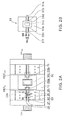
- FIG. 1 is a schematic sectional view of a radio frequency characteristics measurement jig device according to a first embodiment.
- the radio frequency characteristics measurement jig device can be used to measure radio frequency devices such as semiconductor devices and passive components.
- the radio frequency device includes at least one signal terminal.
- the signal terminals include an input terminal and an output terminal.
- the radio frequency characteristics measurement jig device includes a ground conductor part 10, a first coplanar (coplanar waveguide) line 20, a connection substrate 30, and a holding part 60.
- the first coplanar line 20 is provided on the surface 10a of the ground conductor part 10 and connected to a coaxial connector 90a, 90b or the like.
- the radio frequency device 50 is mounted on the surface 10a of the ground conductor part 10.
- the ground conductor part 10 can be provided with a recess, and the radio frequency device 50 can be mounted at the bottom surface thereof. Then, the mounting position can be made accurate.
- connection substrate 30 is attached to the holding part 60 or the like to press the first coplanar line 20 and the signal terminal of the radio frequency device 50 with pressure P.
- a radio frequency signal outputted from the signal generator is inputted to the radio frequency device 50.
- the reflection coefficient (e.g., S 11 and S 22 of the S parameters) of the radio frequency device 50 can be measured by measuring the phase and amplitude of the reflected wave.
- the holding part 60 includes a movable mechanism that can be raised or lowered electrically or manually.
- FIG. 2A is a schematic view showing the planar layout of the radio frequency characteristics measurement jig device.
- FIG. 2B is a schematic plan view of the semiconductor element including a lead terminal.
- FIG. 2A shows a radio frequency characteristics measurement jig device of the semiconductor device such as SiC MESFET, GaN HEMT, and MMIC mounted in a package.
- the first coplanar line 20 includes a first dielectric layer 21 provided on the surface 10a of the ground conductor part 10, a first center conductive layer 22 provided on the surface of the first dielectric layer 21, and first ground conductive layers 26 respectively provided outside first gaps (slots) 24 provided on both sides of the first center conductive layer 22 on the surface of the first dielectric layer 21.
- the characteristic impedance and phase constant can be controlled by changing e.g. the width W of the first center conductive layer 22, the width S of the first gap 24, and the thickness and relative permittivity of the first dielectric layer 21.
- the first ground conductive layer 26 can be connected to the ground conductor part 10 through e.g. a metal layer or the like embedded in a through hole 28 provided in the first dielectric layer 21.
- the chip 50c of the semiconductor element is mounted in a carrier plate package including no leads.
- the rear surface side of the package can be made of a metal plate. This facilitates releasing the heat generated in the chip 50c to the ground conductor part 10.
- the signal terminals 50a, 50b can be made of e.g. a conductive layer provided on the surface of an insulator layer.
- the chip 50c of the semiconductor element can be mounted in a package including leads.
- the signal terminals 51f, 51h can be leads bonded by silver brazing or the like to conductive layers 51a, 51b provided on the surface of an insulator layer 51e.
- the leads can be made of Kovar or the like.
- FIG. 3A is a schematic plan view describing the measurement state.
- FIG. 3B is a schematic sectional view taken along line A-A.
- FIG. 3C is a schematic plan view of the connection substrate.
- FIG. 3D is a schematic sectional view of the connection substrate.
- FIG. 3E is a schematic bottom view of the connection substrate.
- FIG. 3A is a schematic plan view enlarging the region CN of FIG. 2A .
- the connection substrate 30 includes a second coplanar line 37 and a third ground conductive layer 40.
- the second coplanar line 37 includes a second dielectric layer 31 having a first surface 31a and a second surface 31b on the opposite side from the first surface 31a, a second center conductive layer 32 provided on the first surface 31a of the second dielectric layer 31, and second ground conductive layers 36 respectively provided outside second gaps 34 provided on both sides of the second center conductive layer 32.
- the third ground conductive layer 40 is provided on the second surface 31b.
- the second conductive layer 36 and the third conductive layer 40 are connected through a metal layer or the like embedded in a through hole 38 provided in the second dielectric layer 31.
- the second dielectric layer 31 includes a first region LA provided with the second conductive layer 32 and the second ground conductive layer 36 and constituting the second coplanar line, and a second region RA not provided with the second ground conductive layer outside the second conductive layer 32.
- the holding part 60 presses the connection substrate 30 to the first coplanar line 20 and the signal terminal 50a so as to allow electrical continuity between the first center conductive layer 22 and the second center conductive layer 32, to allow electrical continuity between the first ground conductive layer 26 and the second ground conductive layer 36, and to allow electrical continuity between the second center conductive layer 32 of the second region RA of the second dielectric layer 31 and the signal terminal 50a.
- the first ground conductive layer 26 of the first coplanar line 20 and the second ground conductive layer 36 of the second coplanar line 37 of the connection substrate 30 are electrically connected by pressing. This can reduce discontinuity of the ground surface. Furthermore, the connection substrate 30 acts as a conversion circuit from the first region LA being the second coplanar line 37 to the second region RA being the microstrip line. Thus, the signal terminal 50a of the radio frequency device 50 is connected to the microstrip line. Both signal terminals 50a and 50b have a wide width acting as a capacitance to compensate a parasitic inductance of a bonding wire in practical use.
- a reference plane REFin can be accurately defined.
- the input impedance of the radio frequency device 50 at the reference plane REFin can be determined.
- the input matching circuit and the like can be accurately determined based on this input impedance.
- a reference plane REFout can be defined.
- both the first coplanar line 20 on the input side and the first coplanar line 70 on the output side have a characteristic impedance of 50 ⁇ . Then, circuit parameters such as S 21 and S 12 of the S parameters can be determined. In this case, the impedance conversion error due to the use of the connection substrate 30 can be reduced. Thus, the circuit parameters can be accurately determined up to the Ka ( ⁇ 30 GHz) band.
- FIG. 4A is a schematic plan view of a radio frequency characteristics measurement jig device according to a comparative example.
- FIG. 4B is an equivalent circuit diagram thereof.
- the radio frequency device 150 is connected to coplanar lines 120, 170 and microstrip lines by bonding wires BW1, BW2 and the like, and the radio frequency characteristics are measured. Total inspection of product radio frequency devices by wire bonding is not desirable because of appearance problems and increased inspection cost.
- the inductance of the bonding wire occurs between the input side reference plane REFin and the radio frequency device 150, and between the radio frequency device 150 and the output side reference plane REFout.
- the inductance is generally 0.4 nH. This increases the reactance at 12GHz to generally j30 ⁇ .
- radio frequency characteristics measurement it is also possible to perform radio frequency characteristics measurement by bringing a radio frequency probe into contact with the signal terminal or lead of the package without using bonding wires.
- the tip part of the probe is narrow, it is difficult to pass a large current therein.
- the contact resistance is also large.
- the measurement voltage is 10 V or less.
- Semiconductor devices such as GaN HEMT and SiC MESFET often have an operating voltage of 50 V or more.
- FIG. 5A is a schematic plan view of a variation of the connection substrate.
- FIG. 5B is a schematic sectional view of the variation taken along line B-B.
- FIG. 5C is a schematic bottom view of the variation.
- the radio frequency device 50 is a high power HEMT or high power MESFET
- the chip shape is made rectangular, and the width thereof is narrowed.
- the longitudinal direction of the rectangular chip is made generally orthogonal to the extending direction of the coplanar lines and microstrip lines. That is, the cell regions constituting the radio frequency device 50 are arranged in parallel. This facilitates achieving high power.
- the width (denoted by Wc and Wt in FIG. 2B ) of the input/output signal terminal is widened to equalize the distance from the reference plane REFin to each cell region and the distance from each cell region to the reference plane REFout. Then, the device can be operated uniformly in a balanced manner.
- the active region of the radio frequency device 50 is expanded, and the junction capacitance is increased.
- the input/output impedance is lowered.
- the width of the transmission line constituting the rectification circuit is also easily widened. That is, as the width of the signal terminal 50a of the radio frequency device 50 becomes wider, the signal terminal 50a is connected more easily to the external rectification circuit.
- connection substrate 30 shown in FIGS. 5A to 5C , no ground conductive layer is provided on the second surface 31b of the second region RA of the second dielectric layer 31.
- the second region RA is a region converted to a microstrip line.
- discontinuity of the ground surface can be reduced by not providing the ground conductive layer above the second center conductive layer 32.
- the embodiments of the invention provide a radio frequency characteristics measurement jig device capable of measuring radio frequency devices such as semiconductor elements and circuit components at a frequency of 1 GHz to the Ka band.
- the connection substrate connecting the radio frequency device with the transmission line, the influence of the discontinuity of the ground surface can be reduced. This facilitates improving the measurement accuracy.
- the connection substrate provides electrical continuity between the jig and the device mounted in a leadless carrier-plate package.
- the coplanar-microstrip conversion allows the package to have a wide signal terminal 50a, 50b for compensating the parasitic inductance of the bonding wire in practical use. Furthermore, no connection by wiring bonding is performed. This can improve the efficiency of the inspection process without compromising the appearance of products.
- the invention includes a coplanar-microstrip line conversion substrate used for radio frequency characteristics measurement jig devices and the like.
- the coplanar-microstrip line conversion substrate includes a dielectric layer having a first surface and a second surface on the opposite side from the first surface, a center conductive layer provided on the first surface, second ground conductive layers respectively provided outside gaps provided on both sides of the center conductive layer, and a third ground conductive layer provided on the second surface and connected to the second ground conductive layer.
- the dielectric layer includes a first region provided with the center conductive layer and the second ground conductive layer and constituting a second coplanar line, and a second region not provided with the second ground conductive layer outside the center conductive layer.
Abstract
Description
- Embodiments described herein relate generally a radio frequency characteristics measurement jig device.
- Radio frequency semiconductor devices such as GaN HEMT (high electron mobility transistor) and SiC MESFET (metal semiconductor field effect transistor) can provide high power at radio frequencies.
- Thus, further expansion of their application to satellite communication base stations and radar devices is expected.
- Radio frequency semiconductor devices and MMIC (microwave monolithic integrated circuit) are connected to microstrip lines to constitute an electronic device. Thus, radio frequency semiconductor devices and MMIC are preferably mounted in a package with reduced parasitic capacitance and parasitic inductance.
- In this situation, the efficiency of the assembly process can be improved by screening radio frequency devices satisfying the required specifications and incorporating them in the electronic device. Thus, there is demand for a measurement device capable of measuring radio frequency characteristics with high accuracy in a short time.
- It is easy to measure a packaged device having a lead terminal. However, cost of the packaged device becomes higher because the package structure and its manufacturing process become complicated. On the other hand, cost of the lead-less package becomes lower. However, as the lead-less package needs solder or adhesive for measurement, it would be difficult not to leave the solder or the adhesive on the surface of product.
-
-
FIG. 1 is a schematic sectional view of a radio frequency characteristics measurement jig device according to a first embodiment; -
FIG. 2A is a schematic view showing the planar layout of the radio frequency characteristics measurement jig device, andFIG. 2B is a schematic plan view of the semiconductor device including a lead terminal; -
FIG. 3A is a schematic plan view describing the measurement state,FIG. 3B is a schematic sectional view taken along line A-A,FIG. 3C is a schematic plan view of the connection substrate.FIG. 3D is a schematic sectional view of the connection substrate, andFIG. 3E is a schematic bottom view of the connection substrate; -
FIG. 4A is a schematic plan view of a radio frequency characteristics measurement jig device according to a comparative example, andFIG. 4B is an equivalent circuit diagram thereof; and -
FIG. 5A is a schematic plan view of a variation of the connection substrate,FIG. 5B is a schematic sectional view of the variation taken along line B-B, andFIG. 5C is a schematic bottom view of the variation. - In general, according to one embodiment, a radio frequency characteristics measurement jig device includes: a ground conductor part; a first coplanar line; a connection substrate; and a holding part. The radio frequency characteristics measurement jig device is used to measure a radio frequency device including a signal terminal. The first coplanar line includes a first dielectric layer provided on a surface of the ground conductor part, a first center conductive layer provided on a surface of the first dielectric layer, and first ground conductive layers respectively provided outside first gaps provided on both sides of the first center conductive layer on the surface of the first dielectric layer. The connection substrate includes a second dielectric layer having a first surface and a second surface on an opposite side from of the first surface, a second center conductive layer provided on the first surface, second ground conductive layers respectively provided outside second gaps provided on both sides of the second center conductive layer, and a third ground conductive layer provided on the second surface and connected to the second ground conductive layer. The second dielectric layer includes a first region provided with the second center conductive layer and the second ground conductive layer and constituting a second coplanar line, and a second region not provided with the second ground conductive layer outside the second center conductive layer. The holding part is configured to press the connection substrate to the first coplanar line and the signal terminal so as to allow electrical continuity between the first center conductive layer and the second center conductive layer on the first region, to allow electrical continuity between the first ground conductive layer and the second ground conductive layer, and to allow electrical continuity between the second center conductive layer on the second region and the signal terminal.
- Embodiments of the invention will now be described with reference to the drawings.
-
FIG. 1 is a schematic sectional view of a radio frequency characteristics measurement jig device according to a first embodiment. - The radio frequency characteristics measurement jig device can be used to measure radio frequency devices such as semiconductor devices and passive components.
- The radio frequency device includes at least one signal terminal. For instance, in the case where the semiconductor device is a SiC MESFET, GaN HEMT, MMIC or the like, the signal terminals include an input terminal and an output terminal.
- The radio frequency characteristics measurement jig device includes a
ground conductor part 10, a first coplanar (coplanar waveguide)line 20, aconnection substrate 30, and aholding part 60. Thefirst coplanar line 20 is provided on thesurface 10a of theground conductor part 10 and connected to acoaxial connector radio frequency device 50 is mounted on thesurface 10a of theground conductor part 10. Here, theground conductor part 10 can be provided with a recess, and theradio frequency device 50 can be mounted at the bottom surface thereof. Then, the mounting position can be made accurate. - The
connection substrate 30 is attached to theholding part 60 or the like to press thefirst coplanar line 20 and the signal terminal of theradio frequency device 50 with pressure P. As a result, a radio frequency signal outputted from the signal generator is inputted to theradio frequency device 50. The reflection coefficient (e.g., S11 and S22 of the S parameters) of theradio frequency device 50 can be measured by measuring the phase and amplitude of the reflected wave. - In the case where a
first coplanar line 70 is provided on the output side, for instance, the phase of the output radio frequency signal of theradio frequency device 50 is measured by a phase measurement device, and the amplitude thereof is measured by a power meter. Here, theholding part 60 includes a movable mechanism that can be raised or lowered electrically or manually. -
FIG. 2A is a schematic view showing the planar layout of the radio frequency characteristics measurement jig device.FIG. 2B is a schematic plan view of the semiconductor element including a lead terminal. - Here,
FIG. 2A shows a radio frequency characteristics measurement jig device of the semiconductor device such as SiC MESFET, GaN HEMT, and MMIC mounted in a package. - The
first coplanar line 20 includes a firstdielectric layer 21 provided on thesurface 10a of theground conductor part 10, a first centerconductive layer 22 provided on the surface of the firstdielectric layer 21, and first groundconductive layers 26 respectively provided outside first gaps (slots) 24 provided on both sides of the first centerconductive layer 22 on the surface of the firstdielectric layer 21. - The characteristic impedance and phase constant can be controlled by changing e.g. the width W of the first center
conductive layer 22, the width S of thefirst gap 24, and the thickness and relative permittivity of the firstdielectric layer 21. The first groundconductive layer 26 can be connected to theground conductor part 10 through e.g. a metal layer or the like embedded in a through hole 28 provided in the firstdielectric layer 21. - In
FIG. 2A , the chip 50c of the semiconductor element is mounted in a carrier plate package including no leads. In this case, the rear surface side of the package can be made of a metal plate. This facilitates releasing the heat generated in the chip 50c to theground conductor part 10. Thesignal terminals 50a, 50b can be made of e.g. a conductive layer provided on the surface of an insulator layer. - Alternatively, as shown in
FIG. 2B , the chip 50c of the semiconductor element can be mounted in a package including leads. In this case, for instance, thesignal terminals conductive layers insulator layer 51e. The leads can be made of Kovar or the like. -
FIG. 3A is a schematic plan view describing the measurement state.FIG. 3B is a schematic sectional view taken along line A-A.FIG. 3C is a schematic plan view of the connection substrate.FIG. 3D is a schematic sectional view of the connection substrate.FIG. 3E is a schematic bottom view of the connection substrate. -
FIG. 3A is a schematic plan view enlarging the region CN ofFIG. 2A . Theconnection substrate 30 includes a secondcoplanar line 37 and a third groundconductive layer 40. - The second
coplanar line 37 includes asecond dielectric layer 31 having afirst surface 31a and asecond surface 31b on the opposite side from thefirst surface 31a, a second centerconductive layer 32 provided on thefirst surface 31a of thesecond dielectric layer 31, and second groundconductive layers 36 respectively provided outsidesecond gaps 34 provided on both sides of the second centerconductive layer 32. - The third ground
conductive layer 40 is provided on thesecond surface 31b. The secondconductive layer 36 and the thirdconductive layer 40 are connected through a metal layer or the like embedded in a throughhole 38 provided in thesecond dielectric layer 31. Thesecond dielectric layer 31 includes a first region LA provided with the secondconductive layer 32 and the second groundconductive layer 36 and constituting the second coplanar line, and a second region RA not provided with the second ground conductive layer outside the secondconductive layer 32. - The holding
part 60 presses theconnection substrate 30 to the firstcoplanar line 20 and thesignal terminal 50a so as to allow electrical continuity between the first centerconductive layer 22 and the second centerconductive layer 32, to allow electrical continuity between the first groundconductive layer 26 and the second groundconductive layer 36, and to allow electrical continuity between the second centerconductive layer 32 of the second region RA of thesecond dielectric layer 31 and thesignal terminal 50a. - The first ground
conductive layer 26 of the firstcoplanar line 20 and the second groundconductive layer 36 of the secondcoplanar line 37 of theconnection substrate 30 are electrically connected by pressing. This can reduce discontinuity of the ground surface. Furthermore, theconnection substrate 30 acts as a conversion circuit from the first region LA being the secondcoplanar line 37 to the second region RA being the microstrip line. Thus, thesignal terminal 50a of theradio frequency device 50 is connected to the microstrip line. Bothsignal terminals 50a and 50b have a wide width acting as a capacitance to compensate a parasitic inductance of a bonding wire in practical use. - As a result, in
FIGS. 3A and 3B , a reference plane REFin can be accurately defined. For instance, the input impedance of theradio frequency device 50 at the reference plane REFin can be determined. The input matching circuit and the like can be accurately determined based on this input impedance. Furthermore, if a firstcoplanar line 70 is provided also on the output side as shown inFIG. 2A , a reference plane REFout can be defined. - Assume that both the first
coplanar line 20 on the input side and the firstcoplanar line 70 on the output side have a characteristic impedance of 50 Ω. Then, circuit parameters such as S21 and S12 of the S parameters can be determined. In this case, the impedance conversion error due to the use of theconnection substrate 30 can be reduced. Thus, the circuit parameters can be accurately determined up to the Ka (∼30 GHz) band. -
FIG. 4A is a schematic plan view of a radio frequency characteristics measurement jig device according to a comparative example.FIG. 4B is an equivalent circuit diagram thereof. - The radio frequency device 150 is connected to
coplanar lines - Furthermore, as shown in
FIG. 4B , the inductance of the bonding wire occurs between the input side reference plane REFin and the radio frequency device 150, and between the radio frequency device 150 and the output side reference plane REFout. For instance, if the bonding wire has a length of 400 µm, the inductance is generally 0.4 nH. This increases the reactance at 12GHz to generally j30 Ω. - Accurate determination of the input impedance of the radio frequency device at the input side reference plane Din and the output impedance of the radio frequency device at the output side reference plane Dout requires correction by subtracting the inductance of the bonding wire BW1, BW2 from the impedance measured at the reference plane REFin, REFout. However, at high frequencies like the Ka band, it is difficult to accurately correct the inductance of the bonding wire.
- On the other hand, it is also possible to perform radio frequency characteristics measurement by bringing a radio frequency probe into contact with the signal terminal or lead of the package without using bonding wires. However, because the tip part of the probe is narrow, it is difficult to pass a large current therein. Furthermore, the contact resistance is also large. Thus, the measurement voltage is 10 V or less. Semiconductor devices such as GaN HEMT and SiC MESFET often have an operating voltage of 50 V or more. Thus, in the radio frequency characteristics measurement using a probe, it is difficult to measure radio frequency characteristics such as gain and saturation power in the state close to the operation time.
-
FIG. 5A is a schematic plan view of a variation of the connection substrate.FIG. 5B is a schematic sectional view of the variation taken along line B-B.FIG. 5C is a schematic bottom view of the variation. - In the case where the
radio frequency device 50 is a high power HEMT or high power MESFET, the chip shape is made rectangular, and the width thereof is narrowed. The longitudinal direction of the rectangular chip is made generally orthogonal to the extending direction of the coplanar lines and microstrip lines. That is, the cell regions constituting theradio frequency device 50 are arranged in parallel. This facilitates achieving high power. - In such a multi-cell configuration, the width (denoted by Wc and Wt in
FIG. 2B ) of the input/output signal terminal is widened to equalize the distance from the reference plane REFin to each cell region and the distance from each cell region to the reference plane REFout. Then, the device can be operated uniformly in a balanced manner. - Furthermore, in the multi-cell configuration, the active region of the
radio frequency device 50 is expanded, and the junction capacitance is increased. Thus, the input/output impedance is lowered. The width of the transmission line constituting the rectification circuit is also easily widened. That is, as the width of thesignal terminal 50a of theradio frequency device 50 becomes wider, thesignal terminal 50a is connected more easily to the external rectification circuit. - In the second region RA of the
second dielectric layer 31 of theconnection substrate 30 of the invention, no ground conductive layer is provided on thefirst surface 31a side. Thus, even if the width of thesignal terminal 50a is wide, contact of thesignal terminal 50a with the ground conductive layer of theconnection substrate 30 can be suppressed. - In the variation of the
connection substrate 30 shown inFIGS. 5A to 5C , no ground conductive layer is provided on thesecond surface 31b of the second region RA of thesecond dielectric layer 31. The second region RA is a region converted to a microstrip line. Thus, discontinuity of the ground surface can be reduced by not providing the ground conductive layer above the second centerconductive layer 32. - The embodiments of the invention provide a radio frequency characteristics measurement jig device capable of measuring radio frequency devices such as semiconductor elements and circuit components at a frequency of 1 GHz to the Ka band. In the connection substrate connecting the radio frequency device with the transmission line, the influence of the discontinuity of the ground surface can be reduced. This facilitates improving the measurement accuracy. The connection substrate provides electrical continuity between the jig and the device mounted in a leadless carrier-plate package. The coplanar-microstrip conversion allows the package to have a
wide signal terminal 50a, 50b for compensating the parasitic inductance of the bonding wire in practical use. Furthermore, no connection by wiring bonding is performed. This can improve the efficiency of the inspection process without compromising the appearance of products. - Furthermore, the invention includes a coplanar-microstrip line conversion substrate used for radio frequency characteristics measurement jig devices and the like. The coplanar-microstrip line conversion substrate includes a dielectric layer having a first surface and a second surface on the opposite side from the first surface, a center conductive layer provided on the first surface, second ground conductive layers respectively provided outside gaps provided on both sides of the center conductive layer, and a third ground conductive layer provided on the second surface and connected to the second ground conductive layer. The dielectric layer includes a first region provided with the center conductive layer and the second ground conductive layer and constituting a second coplanar line, and a second region not provided with the second ground conductive layer outside the center conductive layer.
- While certain embodiments have been described, these embodiments have been presented by way of example only, and are not intended to limit the scope of the inventions. Indeed, the novel embodiments described herein may be embodied in a variety of other forms; furthermore, various omissions, substitutions and changes in the form of the embodiments described herein may be made without departing from the spirit of the inventions. The accompanying claims and their equivalents are intended to cover such forms or modification as would fall within the scope and spirit of the inventions.
Claims (5)
- A radio frequency characteristics measurement jig device used to measure a radio frequency device including a signal terminal, comprising:a ground conductor part (10);a first coplanar line (20) including a first dielectric layer (21) provided on a surface of the ground conductor part (10), a first center conductive layer (22) provided on a surface of the first dielectric layer (21), and first ground conductive layers (26) respectively provided outside first gaps (24) provided on both sides of the first center conductive layer (22) on the surface of the first dielectric layer (21);a connection substrate (30) including a second dielectric layer (31) having a first surface and a second surface on an opposite side of the first surface, a second center conductive layer (32) provided on the first surface, second ground conductive layers (36) respectively provided outside second gaps (34) provided on both sides of the second center conductive layer (32), and a third ground conductive layer (40) provided on the second surface and connected to the second ground conductive layer (36), the second dielectric layer (31) including a first region provided with the second center conductive layer (32) and the second ground conductive layer (36) and constituting a second coplanar line (37), and a second region not provided with the second ground conductive layer (36) outside the second center conductive layer (32); anda holding part (60) configured to press the connection substrate (30) to the first coplanar line (20) and the signal terminal (50a) so as to allow electrical continuity between the first center conductive layer (22) and the second center conductive layer (32) on the first region, to allow electrical continuity between the first ground conductive layer (26) and the second ground conductive layer (36), and to allow electrical continuity between the second center conductive layer (32) on the second region and the signal terminal (50a).
- The device according to claim 1, wherein
the first coplanar line includes an input side line (20) configured to propagate an input radio frequency signal, and an output side line (70) configured to propagate an output radio frequency signal, and
the connection substrate (30) includes a first substrate connecting the input side line with an input signal terminal (50a) of the radio frequency devices, and a second substrate connecting the output side line with an output signal terminal (50b) of the radio frequency devices. - The device according to claim 1 or 2, wherein the second surface side of the connection substrate (30) is attached to the holding part (60).
- The device according to one of claims 1-3, wherein the second ground conductive layer (36) and the third ground conductive layer (40) are connected through a through hole (38) provided in the second dielectric layer (31).
- The device according to one of claims 1-4, wherein the third ground conductive layer (40) of the connection substrate (30) is provided on the first region of the second dielectric layer (31).
Applications Claiming Priority (1)
| Application Number | Priority Date | Filing Date | Title |
|---|---|---|---|
| JP2013186735A JP2015052574A (en) | 2013-09-09 | 2013-09-09 | High frequency characteristics-measuring jig device |
Publications (2)
| Publication Number | Publication Date |
|---|---|
| EP2846351A2 true EP2846351A2 (en) | 2015-03-11 |
| EP2846351A3 EP2846351A3 (en) | 2015-04-08 |
Family
ID=51220400
Family Applications (1)
| Application Number | Title | Priority Date | Filing Date |
|---|---|---|---|
| EP20140177080 Withdrawn EP2846351A3 (en) | 2013-09-09 | 2014-07-15 | Radio frequency characteristics measurement jig device |
Country Status (3)
| Country | Link |
|---|---|
| US (1) | US9347980B2 (en) |
| EP (1) | EP2846351A3 (en) |
| JP (1) | JP2015052574A (en) |
Cited By (1)
| Publication number | Priority date | Publication date | Assignee | Title |
|---|---|---|---|---|
| CN110380246A (en) * | 2018-04-12 | 2019-10-25 | 和硕联合科技股份有限公司 | The test bench of surface mounted component |
Families Citing this family (1)
| Publication number | Priority date | Publication date | Assignee | Title |
|---|---|---|---|---|
| CN106841709B (en) * | 2017-04-17 | 2019-08-02 | 武汉特视电光技术有限公司 | A kind of MMIC Universal test clamping apparatus |
Family Cites Families (13)
| Publication number | Priority date | Publication date | Assignee | Title |
|---|---|---|---|---|
| US4906953A (en) * | 1988-09-08 | 1990-03-06 | Varian Associates, Inc. | Broadband microstrip to coplanar waveguide transition by anisotropic etching of gallium arsenide |
| JP2763445B2 (en) * | 1992-04-03 | 1998-06-11 | 三菱電機株式会社 | High frequency signal wiring and bonding device therefor |
| JPH06303010A (en) * | 1993-04-14 | 1994-10-28 | Sony Corp | High frequency transmission line and integrated circuit device using the same, and connceting method for high frequency plane circuit |
| US5451567A (en) * | 1994-03-30 | 1995-09-19 | Das; Satyendranath | High power ferroelectric RF phase shifter |
| JP2828009B2 (en) * | 1996-02-16 | 1998-11-25 | 日本電気株式会社 | Microwave / millimeter-wave integrated circuit substrate connection method and connection line |
| JPH1183936A (en) * | 1997-09-08 | 1999-03-26 | Oki Electric Ind Co Ltd | Element evaluation circuit |
| US6070478A (en) | 1998-02-19 | 2000-06-06 | Hewlett-Packard Company | Removable fixture adapter with RF connections |
| US6057700A (en) | 1998-05-06 | 2000-05-02 | Lucent Technologies, Inc. | Pressure controlled alignment fixture |
| WO2001015260A1 (en) * | 1999-08-24 | 2001-03-01 | Paratek Microwave, Inc. | Voltage tunable coplanar phase shifters |
| JP3936858B2 (en) * | 2001-11-01 | 2007-06-27 | 日本オプネクスト株式会社 | Light modulator |
| JP2005331298A (en) | 2004-05-18 | 2005-12-02 | Mitsubishi Electric Corp | Method for measuring characteristics of high-frequency circuit, pattern for calibration, and fixture for calibration |
| GB2477358A (en) | 2010-02-02 | 2011-08-03 | Thales Holdings Uk Plc | RF testing an integrated circuit assembly during manufacture using a interposed adaptor layer which is removed after test to attach the IC to a BGA |
| JP2011196813A (en) | 2010-03-19 | 2011-10-06 | Toshiba Corp | Method and system of testing semiconductor integrated circuit |
-
2013
- 2013-09-09 JP JP2013186735A patent/JP2015052574A/en active Pending
-
2014
- 2014-07-03 US US14/323,041 patent/US9347980B2/en not_active Expired - Fee Related
- 2014-07-15 EP EP20140177080 patent/EP2846351A3/en not_active Withdrawn
Non-Patent Citations (1)
| Title |
|---|
| None |
Cited By (1)
| Publication number | Priority date | Publication date | Assignee | Title |
|---|---|---|---|---|
| CN110380246A (en) * | 2018-04-12 | 2019-10-25 | 和硕联合科技股份有限公司 | The test bench of surface mounted component |
Also Published As
| Publication number | Publication date |
|---|---|
| US9347980B2 (en) | 2016-05-24 |
| JP2015052574A (en) | 2015-03-19 |
| US20150070044A1 (en) | 2015-03-12 |
| EP2846351A3 (en) | 2015-04-08 |
Similar Documents
| Publication | Publication Date | Title |
|---|---|---|
| US8829362B2 (en) | Electronic device having member which functions as ground conductor and radiator | |
| US8558638B2 (en) | Impedance transformer, integrated circuit device, amplifier, and communicator module | |
| KR101077758B1 (en) | High frequency package and manufacturing method thereof | |
| WO2007049376A1 (en) | High-frequency module | |
| US9799599B2 (en) | Matching techniques for wide-bandgap power transistors | |
| US5852391A (en) | Microwave/millimeter-wave functional module package | |
| JP2017121032A (en) | High frequency device | |
| US6466101B2 (en) | Microstrip line-waveguide converter structure, integrated circuit package for high frequency signals provided with this converter structure, and manufacturing method therefor | |
| JP2017163385A (en) | Electronic device and electronic equipment | |
| US9347980B2 (en) | Radio frequency characteristics measurement jig device | |
| CN110663109B (en) | Semiconductor device with a semiconductor device having a plurality of semiconductor chips | |
| US6762493B2 (en) | Microwave integrated circuit | |
| US9041169B2 (en) | Semiconductor packaging container, semiconductor device, electronic device | |
| JP2010034212A (en) | High-frequency ceramic package and method of fabricating the same | |
| JP4206185B2 (en) | High frequency semiconductor device | |
| Kulke et al. | Integration techniques for MMICs and chip devices in LTCC multichip modules for radio frequencies | |
| US8385079B2 (en) | Pressure conductive sheet | |
| JP2021027118A (en) | Semiconductor device | |
| JPH0262064A (en) | Ceramic package | |
| US9449920B2 (en) | Electronic device | |
| JP4344574B2 (en) | Millimeter wave mixer | |
| JP2010117219A (en) | High-frequency characteristics evaluation jig and method for manufacturing semiconductor | |
| Gómez-Duarte et al. | A Practical Approach to the Design and Implementation of Scalable, High-Performance, Custom SMT Packages for mmWave Applications | |
| JPH01316003A (en) | Manufacture of hybrid integrated circuit | |
| JP2010283407A (en) | High frequency ceramic package, and manufacturing method thereof |
Legal Events
| Date | Code | Title | Description |
|---|---|---|---|
| PUAL | Search report despatched |
Free format text: ORIGINAL CODE: 0009013 |
|
| 17P | Request for examination filed |
Effective date: 20140715 |
|
| AK | Designated contracting states |
Kind code of ref document: A2 Designated state(s): AL AT BE BG CH CY CZ DE DK EE ES FI FR GB GR HR HU IE IS IT LI LT LU LV MC MK MT NL NO PL PT RO RS SE SI SK SM TR |
|
| AX | Request for extension of the european patent |
Extension state: BA ME |
|
| PUAI | Public reference made under article 153(3) epc to a published international application that has entered the european phase |
Free format text: ORIGINAL CODE: 0009012 |
|
| AK | Designated contracting states |
Kind code of ref document: A3 Designated state(s): AL AT BE BG CH CY CZ DE DK EE ES FI FR GB GR HR HU IE IS IT LI LT LU LV MC MK MT NL NO PL PT RO RS SE SI SK SM TR |
|
| AX | Request for extension of the european patent |
Extension state: BA ME |
|
| RIC1 | Information provided on ipc code assigned before grant |
Ipc: H01L 21/66 20060101AFI20150227BHEP Ipc: G01R 31/28 20060101ALI20150227BHEP |
|
| STAA | Information on the status of an ep patent application or granted ep patent |
Free format text: STATUS: THE APPLICATION HAS BEEN WITHDRAWN |
|
| 18W | Application withdrawn |
Effective date: 20180830 |